2013 Vol.59 No. Power Semiconductors Contributing in Energy Management
|
|
|
- Millicent Newton
- 5 years ago
- Views:
Transcription


1 4 213 Vol.59 No. Power Semiconductors Contributing in Energy Management

2 213 Vol.59 No. 4 Power Semiconductors Contributing in Energy Management Cover Photo: FUJI ELECTRIC REVIEW vol.59 no date of issue: December 3, 213 editor-in-chief and publisher editorial office EGUCHI Naoya Corporate R & D Headquarters Fuji Electric Co., Ltd. Gate City Ohsaki, East Tower, 11-2, Osaki 1-chome, Shinagawa-ku, Tokyo , Japan Fuji Electric Journal Editorial Office c/o Fuji Office & Life Service Co., Ltd. 1, Fujimachi, Hino-shi, Tokyo , Japan
3 Contents Power Semiconductors Contributing in Energy Management 1,7 V Withstand Voltage SiC Hybrid Module 218 KOBAYASHI Kunio KITAMURA Shoji ADACHI Kazuya Ultra-Compact, High-Reliability All-SiC Module 221 NAKANO Hayato HINATA Yuichiro HORIO Masafumi New Assembly Technologies for T jmax =175 C Continuous Operation 226 Guaranty of IGBT Module MOMOSE Fumihiko SAITO Takashi NISHIMURA Yoshitaka High-Power IGBT Modules for 3-Level Power Converters 23 CHEN Shuangching OGAWA Syogo ISO Akira Packaging Technology of IPMs for Hybrid Vehicles 235 GOHARA Hiromichi ARAI Hirohisa MOROZUMI Akira IGBT Modules with Pre-Applied TIM 241 ISO Akira YOSHIWATARI Shinichi 2nd Generation LLC Current Resonant Control IC, FA6AN Series 245 CHEN Jian YAMADAYA Masayuki SHIROYAMA Hironobu One-Chip Linear Control IPS, F516H 251 NAKAGAWA Sho OE Takatoshi IWAMOTO Motomitsu Supplemental Explanation 3-level power conversion 255 New Products Top Runner Motor of Fuji Electric- 256 Premium Efficiency Motor MLU and MLK Series High-Voltage Air Load Break Switch (LBS) 259 Discrete RB-IGBT FGW85N6RB 262 FUJI ELECTRIC REVIEW vol.59 no.4 213

4 1,7 V Withstand Voltage SiC Hybrid Module KOBAYASHI Kunio KITAMURA Shoji ADACHI Kazuya ABSTRACT In place of Si devices, silicon carbide devices (SiC devices) featuring heat resistance and high breakdown fi eld tolerance are raising expectations for efficiency improvement and miniaturization of equipment. Fuji Electric is moving ahead with the development of a 1,7 V withstand voltage SiC hybrid module for high-effi ciency inverters (69 V series). A SiC-SBD chip jointly developed with the National Institute of Advanced Industrial Science and Technology has been applied to a freewheeling diode (FWD), and a Fuji Electric s V-Series IGBT chip has been applied to an insulated gate bipolar transistor (IGBT). By improving leakage current and switching characteristics, the module has been verified to be capable of reducing generated loss by approximately 26% in a 3 A product compared to the conventional Si modules. 1. Introduction Faced with the need to prevent global warming, the urgent task of reducing emissions of greenhouse gases such as CO 2 is greater than ever. One of the means to realize this is to ensure energy saving in power electronics devices. Highly efficient inverters are an important aspect of this, and they require technological innovation for components such as power devices, circuits and controls. In particular, there is a strong demand for lowering power dissipation in power devices that are the main elements of inverters. An insulated gate bipolar transistor (IGBT), a major power device, has used a silicon (Si) IGBT chip and free-wheeling diode (FWD) chip so far. However, Si devices are hitting the theoretical limit in terms of performance based on their physical characteristics. For this reason, there are high expectations now for silicon carbide (SiC) devices because of their properties of heat resistance and high breakdown field tolerance, and it is hoped they will improve equipment efficiency and achieve miniaturization. This paper describes a 1,7 V withstand voltage SiC hybrid module that deploys SiC devices. 2. Product Features Fuji Electric has so far completed the development of 6 V withstand voltage SiC- Schottky barrier diode (SBD) for 2 V systems and 1,2 V withstand voltage SiC-SBD for 44 V systems, followed by successful commercialization of an SiC hybrid module that combines these SiC-SBDs and Si-IGBT. SiC-SBD has low Electronic Devices Business Group, Fuji Electric Co., Ltd. Corporate R&D Headquarters, Fuji Electric Co., Ltd. Fig.1 M277 package resistance and superior switching characteristics in comparison with an Si-PIN diode, a conventional high blocking voltage FWD. With these features, the SiC hybrid module has a capacity to reduce generated loss by approximately 26% compared with conventional Si- IGBT modules. The development of a 1,7 V withstand voltage SiC hybrid module is currently underway for 69 V input inverters. The M277 package (see Fig. 1) has been adopted for the SiC hybrid module to allow for easy changeover from conventional Si modules, which use the same package. Fuji Electric developed an SiC-SBD chip jointly with the National Institute of Advanced Industrial Science and Technology, followed by the Company s launch of a mass-production line. This chip has been applied to FWD, while IGBT has been equipped with Fuji Electric s latest product, the sixthgeneration V-Series IGBT chip. 3. Features 3.1 Forward characteristic of FWDs Figure 2 illustrates the FWD forward-direction 218
5 6 Si module 1 SiC hybrid module Si module IF (A) V F (V) Fig.2 Forward characteristic of FWDs VF Si module Tj Fig.3 Temperature dependency of FWDs Si module characteristic of the SiC hybrid module and Si module, and Fig. 3 illustrates the temperature dependency. With a junction temperature at 15 C and rated current of 3 A, the forward direction voltage V F is on the same level as the Si module V F. Owing to its strong positive temperature coefficient, the SiC hybrid module creates smaller current imbalance in multi-parallel connections Rated current Io = 3A SiC hybrid module VCE ICES (ma) C 125 C 5 SiC hybrid module 1, V CE (V) Si module 1,5 Fig.4 Leakage current temperature dependency 2, 3.2 Leakage current Figure 4 depicts the leakage current temperature dependency of an SiC hybrid module and Si module. While the leakage current I CES of the SiC hybrid module is nearly ten times greater than that of the Si module at the rated voltage at 125 C (1,7 V), this difference shrinks to approximately twice at 15 C. The difference in leakage current value between 125 C and 15 C under the rated voltage is smaller in the SiC hybrid module compared to that in the Si module. Therefore, SiC-SBD has a smaller leakage current temperature dependency compared with Si-FWD. This is because SiC s band gap is approximately three times that of Si, and as SiC-SBD operates at a higher electrical field than Si-FWD, thus the leaked current of SiC-SBD becoming predominantly tunneling current and making it less susceptible to temperature fluctuations. For these reasons, the SiC hybrid module can, like the V-Series, perform in a high temperature environment (1). 3.3 Switching (1) Reverse recovery loss Figure 5 illustrates the reverse recovery loss of the SiC hybrid module and Si modules. The SiC hybrid module scarcely has any peak reverse recovery current. This is explained by the fact that SiC-SBD is a unipolar device, and so it causes no minority carrier injection. The reverse recovery loss of 3 A products is lower than that of the Si module by approximately 83%. (2) Turn-on loss Figure 6 shows the turn-on losses of the SiC hybrid Err (mj) Fig.5 Reverse recovery loss V CC=9V, R g=+4.7, V GE=±15V, T j=125 C Si module 3 I F (A) 4 SiC hybrid module 5 6 issue: Power Semiconductors Contributing in Energy Management 1,7V Withstand Voltage SiC Hybrid Module 219
6 Eon (mj) Fig.6 Turn-on loss V CC=9V, V GE=±15V, R g=+4.7, T j=125 C Si module 2 3 I C (A) SiC hybrid module Total loss (W) E rr V F E off E on V CE(sat) SiC hybrid module Fig.8 Inverter generated loss 2 Si module f c (khz) Eoff (mj) V CC=9V, V GE=±15V, R g=+2.4, T j=125 C 1 Fig.7 Turn-off loss Si module 2 module and Si module. The peak reverse recovery current of SiC-SBD affects the IGBT turn-on current in the opposing arm, leading to a lower turn-on loss. The turn-on loss of a 3 A product is lower than that of the Si module by approximately 4%. (3) Turn-off loss Figure 7 depicts the turn-off losses of the SiC hybrid module and Si module. The surge peak voltage of the SiC hybrid module at a turn-off can be expressed as shown in Formula (1). Provided that the IGBT element characteristics and inductance of the main circuit are equal, the difference in the transient on-voltage becomes the difference in the surge voltage. The drift layer of SiC-SBD has extremely low resistance compared to Si-FWD, and this lowers the transient on-voltage. Therefore, the surge voltage at turn-off is kept low, and hence there is a low turn-off loss. di c V sp = V cc + L s + V fr... (1) d t V sp : surge peak voltage V cc : applied voltage L s : main circuit inductance I c : collector current V fr : transient on-voltage 3 I C (A) SiC hybrid module Inverter generated loss Figure 8 shows the inverter generated losses of the SiC hybrid module and Si module. The SiC hybrid module s total loss at the carrier frequency f c of 2 khz is lower than that of the Si module by approximately 26%. As the loss increase rate of the SiC hybrid module is more suppressed than the Si module at higher carrier frequencies, the SiC hybrid module has an advantage over the Si module in performing at high frequencies. 4. Postscript The SiC hybrid module is a product deploying SiC-SBD, which was developed jointly with the National Institute of Advanced Industrial Science and Technology, and Fuji Electric s latest product, the sixth-generation V-Series Si-IGBT. SiC hybrid module has successfully attained a significant loss-reduction within the device, enabling an efficiency enhancement for inverters to a great extent. We will expand the range of SiC-chip-applied products and develop product families in the future to contribute to energy conservation. We would like to thank everyone at the Advanced Power Electronics Research Center of the National Institute of Advanced Industrial Science and Technology who contributed to the development of SiC- SBD chip. References (1) Nakazawa, M. et al. Hybrid Si-IGBT and SiC-SBD Modules. FUJI ELECTRIC REVIEW. 212, vol.58, no.2, p FUJI ELECTRIC REVIEW vol.59 no.4 213
7 Ultra-Compact, High-Reliability All-SiC Module NAKANO Hayato HINATA Yuichiro HORIO Masafumi ABSTRACT SiC devices have excellent characteristics that realize high blocking voltage, low power dissipation, high-frequency and high-temperature operation. Fuji Electric s All-SiC module features direct bonding layout for semiconductors and a plastic molding structure. Compared with the conventional product, the All-SiC module achieves signifi cant improvement of 5% in footprint, 75% lower PN and gate inductances, and approximately 35% lower switching loss. Moreover, for using high power drives, switching is demonstrated in the case of 4 modules being connected in parallel. The All-SiC module is verifi ed to have suffi cient reliability in high temperature and humidity, in addition to power cycling, and is better than the conventional products. 1. Introduction In the power electronics field, a power module serves as central components in a highly efficient power conversion society. There are many applications which need a power module not only in the renewable energy field such as in solar and wind power, but also in in-vehicle field such as in a hybrid electric vehicle (HEV) and electric vehicle (EV). On the other hand, because of the characteristics of Si devices, the performance of the Si module is approaching its limit. Therefore, new wide band gap semiconductors such as SiC (silicon carbide) and GaN (gallium nitride) have enough potential to be the nextgeneration device instead of Si (1). Regarding this background, the SiC device is expected to be an excellent device which has a high blocking voltage, low power dissipation, high-frequency and high-temperature operation compared with conventional devices. This paper describes the All-SiC module that an SiC-metal-oxide-semiconductor field-effect transistor (MOSFET) and SiC-Schottky barrier diode (SBD) are mounted. 2. Comparison of packaging technology Figure 1 shows a comparison of the structure crosssection of the new and conventional structures. The new structure aims to maximize the SiC device property as mentioned. The existing structure is the conventional Si module. In the new structure, device connections are performed by using a power substrate to the semiconductor element (power chip) with surface bonding. Heat dissipation performance is improved by using a thick copper substrate to the AMB substrate* 1. Corporate R&D Headquarters, Fuji Electric Co., Ltd. Silicone gel Epoxy resin AMB substrate Aluminum wire Power chip Solder (a) Existing structure Power substrate Copper pin (b) New structure Ceramic substrate Ceramic substrate DCB substrate External terminal Resin case Metal base External terminal Thick copper substrate Fig.1 Cross-section of the existing structure and new structure In order to decrease mechanical stress inside a module, optimization of the linear expansion coefficient of constitution materials and a resin sealing structure are applied. Figure 2 shows the picture of the All-SiC module that is rated 1,2 V/1 A and the Si module of the same rating. Table 1 shows a summary of comparing these two in terms of footprint size and inductance. Regarding this table, the All-SiC module has dramatically reduced the footprint size by 5% and lowered the *1: AMB substrate: an insulating substrate for radiating heat which is composed of a thick copper substrate and a ceramic substrate joined together via active metal brazing (AMB) method issue: Power Semiconductors Contributing in Energy Management 221

8 75 5 Switching loss Loss due to on-resistance Si-IGBT&FWD SiC-MOSFET &SBD 24.7mm 62.6mm 34.mm 92.mm Loss (W) 25 (a) All-SiC module (b) Si module Fig.2 All-SiC module and Si module Table 1 Comparison between the All-SiC module and the Si module Package structural characteristic Reduction rate (comparison between the existing structure and the new structure) Footprint 5% Inductance between PN 75% Gate inductance 75% PN and gate inductance by 75% compared with the Si module. Therefore, the new structure has compact and lower inductance advantages for high speed and high temperature drive which is able to maximize the SiC device characteristics Switching frequency (khz) Fig.3 Switching frequency dependency of occurrence loss of the SiC device and the Si device Switching frequency 1 khz (1 A) 4 khz (1 A) Si module 1/2 footprint 1/4 footprint All-SiC module 3. The All-SiC Module for Solar PCS 3.1 Effect of mounting All-SiC module for high frequency switching The All-SiC module, for which development is in progress, is ultra-compact and has high-speed switching capability. In the case of high-frequency switching, it is possible to shrink the size of subsidiary parts such as reactors because of its frequency dependency. Therefore, high-speed switching enables to downsize the entire system volume. This scenario ends up with a power conditioner to downsize the photovoltaic power generation (solar PCS) described in this paper. At the advantage of high-frequency switching capability, the All-SiC module generates lower loss, which means there is no requirement to increase the number of modules instead of having multipul modules in parallel. Figure 3 shows the switching frequency dependency of loss of the SiC and the Si modules. This is the result of calculating loss for switching frequency in the case of the SiC and the Si device being mounted on the 2-in-1 module. For the module composed of the Si device, switching frequency increases the switching loss. On the other hand, the All-SiC module does not increase switching loss even though the All-SiC module works under high switching frequency. Therefore, the All-SiC module have been reduced the loss, which depends on switching frequency. 1 khz (1 A) 1/8 footprint Fig.4 Effect of All-SiC module for high-frequency purpose Figure 4 shows the impact of the All-SiC module for a high-frequency application. This is a comparison of the number of All-SiC and Si modules when the loss is roughly even. For example, at the switching frequency of 1 khz, the All-SiC and the Si modules have almost identical losses. In this case, the footprint of the All- SiC module is 1/2 of the Si module. At the switching frequency is 4 khz, the loss of the Si module should be double compared with the All-SiC. Therefore the loss of the two Si modules and the one All-SiC module become almost even. In the terms of footprint, the All- SiC module has 1/4 that of the Si module. When the switching frequency is 1 khz, the downsizing effect becomes so significant that the All-SiC footprint is 1/8 of the Si module. 222 FUJI ELECTRIC REVIEW vol.59 no.4 213

9 3.2 Switching result Since it is necessary to clarify the advantage of the All-SiC structure, the SiC devices were put into the new and conventional structures and evaluated their packaging technology. The evaluation conditions of switching characteristics were as follows: V ds is 6 V, I d was 1 A, V g was +15/ 5 V, R g was 6.8 Ω and T j was 2 C. Figure 5 shows the temperature dependence of the surge voltage that occurs at turn-off. With the new structure, the surge voltage is decreased by approximately 5 V compared to the existing structure. This advantage is accomplished by low inductance. In addition, the gap of the surge voltage at room temperature and 2 C is approximately 1 V. The temperature dependency of switching loss of the existing and the new structures is shown in Fig. 6. Switching loss is the total loss of turn-on, turn-off and reverse recovery. The evaluation condition was the same as in the previous surge voltage test. The SiC devices are mounted on both structures, and therefore the temperature dependency is low. Switching loss of the new structure becomes approximately 35% lower than the existing structure due to the low inductance. 9 P 45 to 95V N M All-SiC module (1,2V/1A) Bidirectional switch Prototype inverter (3V/2kW) 3 V Fig.7 Circuit structure of solar PCS inverter section Efficiency (%) A U V W issue: Power Semiconductors Contributing in Energy Management Turn-off surge voltage Vcep 85 8 Existing structure New structure Fig.5 Temperature dependence of surge voltage at turn-off Existing structure New structure Fig.6 Temperature dependency of switching loss 96 1, Fig.8 Effi ciency of solar PCS 2, 3, AC output (W) 4, 3.3 Continuous operation The All-SiC module is integrated in the proto-type solar PCS inverter application. Figure 7 shows the circuit structure of the inverter. It uses 3-level control that enables more higher efficiency and downsizing of the system compared with the existing 2-level control including the bidirectional-switching. In this case the switching frequency is 2 khz. Figure 8 shows the efficiency of solar PCS is about 99% at the maximum. Solar PCS efficiency means the efficiency when converting the electric power generated by a solar panel into the intended voltage. In addition, because the module size becomes smaller, it is possible to downsize the volume of the conventional solar PCS chassis to approximately 75% (2). 4. High Power All-SiC Module Concept 5, A high power SiC module is expected to be part of a future product strategy. It can be achieved by producing large size of the SiC chip; however, there are issues such as the high defect density of the SiC substrate and in the case where the chip area becomes Ultra-Compact, High-Reliability All-SiC Module 223
10 V ds V ds larger, reduction in the yield rate becomes low. One of the options to solve this issue is to increase the output capacity of the module by connecting the chip in parallel instead of producing large size of the SiC chip. It is possible to connect the All-SiC module in parallel to have further high-power capability. Here, it is important to design the high-power All-SiC module to have low inductance by having a bus bar connection. Switching evaluation of the All-SiC module in parallel was performed. The All-SiC module comprised a 1,2 V/4 A module by connecting 4 modules of 1,2 V/1 A module. The evaluation conditions were as follows: V ds was 6 V, I d was 4 A, V g was +15/ 5 V and R g was 9.7 Ω. In the high-power module, because the output power is high, a turn-off surge voltage issue emerges. With the high-power module for which development is in progress, this issue is solved by connecting the module in parallel with a low inductance bus bar. This design has to be used in order to prevent losing the low inductance advantage of the All- SiC module. Figure 9 shows the switching waveforms of the high-power module. There is no critical failure as oscillation and the excessive surge voltage. It was demonstrated that switching is feasible even when 4 modules of the All-SiC are connected in parallel. 5. Reliability (a) Turn-on waveform (b) Turn-off waveform Fig.9 Switching of large-capacity module It was confirmed that the All-SiC module has better reliability than the existing Si module by performing multiple tests as power cycle, heat cycle, high-temperature and high-humidity reverse bias tests. In the power cycle test, it was found that the new structure has 1 times the power cycle capability compared with the existing structure when T jmax is 2 C ( T j=175 C). I d I d It is important to clarify the humidity capability of the All-SiC module because it has a totally different structure compared with the Si module. Therefore, high-temperature and high-humidity reverse bias tests are important. The new structure is molded by resin, and the resin easily absorbs moisture under a highly humid environment and the moisture is likely to be a cause of mechanical or electric failure. Figure 1 shows the result of high-temperature and high-humidity reverse bias tests (leak current). This is the electric characteristics trace result during reliability test, which was continued up to a cumulative total of 3, hours with the temperature of 85 C and relative humidity of 85%, and by applying V to the V g and reverse bias voltage was 96. This 3,-hour test was conducted to confirm performance up to three times the Fuji Electric standard in the high-temperature and high-humidity environment load test. In an arbitrary time, samples (N=5) were extracted to check leak current I DSS and evaluated at 1,2 V to check reverse bias voltage V ds and abnormality in characteristics. The module was abandoned under a high-temperature and high-humidity environment for as long as 3, hours with reverse bias applied simultaneously, no remarkable increase in leak current was found and Leak current IDSS (μa) , 2, Applied time (h) V ds 1,2 V 3, Fig.1 Result of high-temperature and high-humidity reverse bias test (leak current) Gate leak current IGSS (μa) , 2, Applied time (h) V gs 25 V 3, Fig.11 Result of high-temperature and high-humidity reverse bias test (gate leak current) 224 FUJI ELECTRIC REVIEW vol.59 no.4 213
11 the value was approximately equal to the initial. Transition of the gate leak current I GSS in the similar reliability test is shown in Fig. 11. Evaluation condition of I GSS is the gate leak current when V gs +25 V is applied. There is no critical behavior from the evaluation of I GSS and since the leak current is stable, deterioration of a gate structure under an environment with high temperature and high humidity is not observed. As a result, it was confirmed that the new structure that is applied to the All-SiC module is more reliable than the existing products, under a high-humidity environment. 6. Postscript Fuji Electric is progressing with the development of the All-SiC module in the terms of maximizing the SiC device properties such as high blocking voltage, low power dissipation, high-frequency and high-temperature operation. The All-SiC module has sufficient reliability compared with a conventional Si packaging technology. By applying the All-SiC module, downsizing and high efficiency drive are realized. In particular, the high-frequency operation maximizes the characteristics of the downsizing effect. In the future, Fuji Electric will expand the range of applications via module capacity enlargement, and contribute to the development of power electronic society. References (1) Prof. B. Jayant Baliga. The Role of Power Semiconductor Devices in Creating a Sustainable Society. Plenary Session APEC 213. (2) Matsumoto, Y. et al. Power Electronics Equipment Applying SiC Devices. FUJI ELECTRIC REVIEW. 212, vol.58, no.4, p issue: Power Semiconductors Contributing in Energy Management Ultra-Compact, High-Reliability All-SiC Module 225
12 New Assembly Technologies for T jmax =175 C Continuous Operation Guaranty of IGBT Module MOMOSE Fumihiko SAITO Takashi NISHIMURA Yoshitaka ABSTRACT In order to meet the needs for miniaturization and cost reduction of inverters, IGBT modules are required to offer higher power density than ever. Fuji Electric has developed a new aluminum wire, solder alloy and surface electrode protection layer to improve the continuous operating temperature of an IGBT module from the conventional 15 C to 175 C, thereby realizing higher power density. A power cycle lifetime has been more than doubled compared with the conventional products in all temperature ranges, and thus 2% improvement of inverter maximum output can be expected. 1. Introduction General-purpose inverters are widely used and demand for them is expanding as they contribute to significant energy saving. There is a strong market need for energy efficiency and miniaturization as well as for a comprehensive reduction of costs including system development costs (1). In order to meet such market demand, Fuji Electric has been working on loss improvement and miniaturization of insulated gate bipolar transistor (IGBT) chips, which are a main component of an IGBT mounted on a general-purpose inverter. The V-Series of IGBT modules has improved the guaranteed continuous operation at 15 C, which is 25 C higher than the IGBT module operation temperature of the U-Series. This has been done to support miniaturization and cost reduction of inverter systems as a whole. Figure 1 illustrates the transition of rated IGBT module chip area (1,2 V; 5 A). As there is limited room for further improving the power losses of IGBT Chip area ratio with the L-Series as 1% (%) Junction temperature 125 C 15 C 175 C 2 C L-Series N-Series S-Series U-Series 25 (Year) V-Series Next generation 21 Fig.1 Transition of IGBT chip area (1,2 V/ 5 A) SiC devices Corporate R&D Headquarters, Fuji Electric Co., Ltd. chips, we considered miniaturizing and higher power density of IGBT modules by raising the upper limit of the operating temperature. It is estimated that a 2% improvement in the output of a general-purpose inverter is expected when the upper limit of the operating temperature is raised to 175 C from the conventional 15 C. This article will describe the assembly technology for IGBT modules that realizes highly reliable and continuous operation at T jmax 175 C. 2. Technical Challenges to Guarantee Continuous Operation at 175 C One of the important elements in realizing guaranteed continuous operation at 175 C is power cycle lifetime. Raising the maximum operational temperature from the conventional 15 C by 25 C means there is an increase of thermal stress on component materials. It also increases the temperature fluctuation range between operation and downtime. Thus the materials need guaranteed resistance against more thermal fatigue than the previous product. Figure 2 shows the power cycle lifetime of previous modules at fixed maximum operational temperature T jmax with a cumulative failure rate of 1%. The lifetime is reduced by 3% to 5% as T jmax increases to 175 C from 15 C. It is therefore essential to create a highly reliable assembly that guarantees a power cycle lifetime equal to that of previous 15 C-range products and yet is operable at a T jmax of 175 C. It is generally considered that fractures in an IGBT module incurred in the power cycle test are mainly due to fatigue from repeated stress applied between components differing in coefficient of thermal expansion during temperature fluctuations (2). In a continuous operation at T jmax 175 C, the effect from a metallic microstructure change in the components 226
 Bonding wire (b) Bond layer between chip and insulating substrate IGBT chip side Sn-Ag solder Insulating substrate side 15 (c) Chip surface")

. σ y=σ+kd 1/2.")

13 Power cycle lifetime (cycle) % Cumulative failure rate = 1% Estimated lifetime Testing conditions T on=2 s, T off =18 s T j ( C) 5% T jmax=15 C T jmax=175 C Fig.2 Power cycle lifetime in the conventional structure (a) Bonding wire (b) Bond layer between chip and insulating substrate IGBT chip side Sn-Ag solder Insulating substrate side 15 (c) Chip surface electrode Aluminum grains 3. New Bonding Technology to Achieve High Reliability 3.1 New aluminum wire Figure 4 shows a cross-section of aluminum wire after a power cycle test (T jmax=175 C; T j=75 C). The bond was broken as the cracks developed within the aluminum wire material. This suggests that the lifetime primarily depends on the material strength of the aluminum wire. Power cycle test at T jmax 175 C suggests that aluminum particles in the wire coarsen as they recrystallize because the temperature is within the recrystallization temperature range of the material. The following Hall-Petch Equation expresses the relationship between metallic grain diameter and strength (3). σ y=σ+kd 1/2... (1) σ y : Yield stress d : Average grain diameter of the metal σ, k : Material dependent constants The Hall-Petch Equation indicates that growth in metal grain size weakens the material. Therefore, Fuji Electric has developed new aluminum wire that has a recrystallization temperature higher than 175 C. Figure 5 illustrates a cross-section of aluminum wire issue: Power Semiconductors Contributing in Energy Management Fig.3 Fractures after power cycle testing (T jmax = 175 C) must be taken into account in addition to the repetitive stress. The components in question are solder and aluminum. We therefore observed fractures in a module subject to the power cycle test at the continuous operational temperature of T jmax 175 C. Figure 3 illustrates fractures under power cycle testing (T jmax=175 C). There are mainly three parts susceptible to fracture. (a) Bonding wire Sheer stress created by the difference in coefficient of thermal expansion between aluminum wire and silicon (Si) chip causes cracks in the base material, and eventually the wire detaches. (b) Bonding between chip and insulating substrate The solder used between the chip and insulating substrate undergoes microstructural changes and thermal fatigue, which exacerbate the development of cracks in the solder bonding portion. (c) Chip surface electrode Cracks are caused in the chip surface electrode due to coarsening of aluminum grains and the fact that aluminum has a coefficient of thermal expansion that is different from that of silicon. In order to secure continuous operation at T jmax 175 C, lifetime of material in these three fracture areas need to be improved. Aluminum wire Chip Conventional aluminum wire New aluminum wire Before power cycle test (initial) 3 μm Chip this side 3 μm Before power cycle test (initial) 3 μm Chip this side 3 μm 2 μm Fig.4 Cross-section of the bonding wire after power cycle testing After power cycle test (25 k cycles) After power cycle test (35 k cycles) Fig.5 Cross-section of aluminum wire before and after power cycle test (T jmax = 175 C) New Assembly Technologies for T jmax=175 C Continuous Operation Guaranty of IGBT Module 227
14 before and after a power cycle test (T jmax=175 C). This is a cross-section image using electron back scatter diffraction (EBSD). The aluminum grain growth was observed in the conventional wire after the power cycle test, but there was no change in the grain in the new aluminum wire. Therefore, it is supposed that the base material strength of the aluminum wire is not compromised by the power cycle test. 3.2 New solder There is a concern that the degradation of solder layer between the chip and substrate due to heat and thermal fatigue is accelerated during the continuous operation at T jmax 175 C. We attempted to reinforce the soldering material against high temperature, based on microstructural considerations. There are two methods to strengthen metal with additional elements: precipitation strengthening and solid-solution strengthening. Figure 6 shows structural models of solder before and after a thermal aging process* 1. The diagrams depict microstructural changes in the metal caused by the strengthening methods. Sn-Ag solder is the representative of precipitation strengthening. In this case, Ag 3Sn minuscule inter-metallic compounds precipitate between Sn particles, reinforcing the yield point of the grain boundary and preventing the development of cracks. However, Sn grains grow and Ag 3Sn aggregates under high temperature, resulting in cracks. On the other hand, Sn solder with added Sb and In within the solid solubility limit is the model for the solid-solution strengthening. The particles of Sb and In dissolve in the Sn grains to suppress coarsening under high temperature. Figure 7 is an illustration of the tensile strength variance in solder after thermal aging test. Stored under the conditions of 15 C and 175 C for 1, hours, Sn-Ag solder significantly weakens from its initial Precipitation strengthening type Solid solution strengthening type Initial state (before thermal aging) Ag 3 Sn Sn SnSb (solid solution) After reliability test (after thermal aging) Cracks Coarsening growing Fig.6 Structural diagram of solder before and after thermal aging *1: Aging: a phenomenon in which metallic properties (for example hardness) change over time. Tensile strength (%) 1 5 Sn-Sb solder Initial state , Sn-Ag solder 175 1, ( C) (time) Fig.7 Tensile strength variance in solder after thermal storage test Tensile strength (%) Sn-Sb solder New solder Fig. 8 Tensile strength of Sn-Sb and new solder state while Sn-Sb maintains its strength. We also conducted a power cycle test (T jmax=175 C) using samples of both Sn-Ag and Sn-Sb solder to compare the effects on the power cycle lifetime. As a result, we verified that Sn-Sb had superior improvement of power cycle lifetime over Sn-Ag. Furthermore, by adding Sb in excess of the solid solubility limit, residual Sb precipitates as SnSb, creating an effect of the solid-solution strengthening and precipitation strengthening combined (4). Leveraging this feature, Fuji Electric has developed a Sn-Sb-based new solder with additional new elements having characteristics of both solid solution strengthening and precipitation strengthening. This will be followed by mass production of the next-generation IGBT modules in the near future. Figure 8 shows the tensile strength of Sn-Sb and new solder. The new solder has a higher tensile strength than Sn-Sb solder. We have also verified its enhanced power cycle lifetime over Sn-Sb in a power cycle test (T jmax=175 C). 3.3 New surface electrode protection layer Si chip surface electrode is usually made of pure aluminum or with Si or Cu compounds. In power cycle test, the surface electrode sustains stress due to coarsening of aluminum grains from the heat generated in 228 FUJI ELECTRIC REVIEW vol.59 no.4 213
 Conventional aluminum surface electrode the chip as well as from the difference in coefficient of thermal expansion from the Si chip, resulting in cracks caused in the")

15 at T jmax 175 C over the target power cycle lifetime of conventional technology at T jmax 15 C. The lifetime was more than doubled at all temperature regions. 5. Postscript 2 μm 2 μm (a) Conventional aluminum surface electrode the chip as well as from the difference in coefficient of thermal expansion from the Si chip, resulting in cracks caused in the surface electrode as well as in the aluminum wire bonding (5). In order to prevent this, we have developed a structure with Ni, which has a coefficient of thermal expansion closer to silicon than to aluminum, forming a layer over the aluminum electrode to reduce the stress exerted upon it. Figure 9 illustrates the observation results from the power cycle test (T jmax=175 C) for a chip surface electrode without aluminum wire bonding. It is possible to lessen degradation by forming a protection layer over the aluminum electrode using Ni. 4. Effects of New Technology (b) Aluminum surface electrode with Ni protection layer Fig.9 Surface electrode after power cycle test (T jmax=175 C) We prepared a sample to which we applied the three new technologies described in Section 3 and conducted power cycle test. Figure 1 shows the test results (T jmax=175 C). The new technology yielded a significant improvement Power cycle lifetime (cycle) Estimated lifetime T jmax 175 C (new technology) T jmax 15 C (conventional technology) Cumulative failure rate = 1% T j ( C) Fig.1 Power cycle test results (T jmax = 175 C) 15 We have described the IGBT module assembly technology that accomplished reliable continuous operation at T jmax 175 C. The developed IGBT module has guaranteed continuous operation at T jmax 175 C while achieving a longer lifetime than conventional modules as a result of combining three new bonding technologies: new aluminum wire with high thermal resistance, new solder with high strength at high temperature and a new surface electrode protection layer providing high strength at high temperature and lower thermal stress between silicon and aluminum. These technologies can be deployed without changing the current manufacturing processes at Fuji Electric, enabling easy mass production of items with guaranteed continuous operation at T jmax 175 C. By increasing high power density, improvements are expected to be made to the maximum power output of general-purpose inverters. We will continue our efforts with the development and expansion of offerings of the T jmax 175 C continuous operation guaranteed IGBT module family, and contribute to the improvement of industrial equipment for higher efficiency and better energy saving. References (1) Sakai, T. et al. Latest Technology for General-purpose Inverters and Servo Systems. FUJI ELECTRIC REVIEW. 29, vol.55, no.4, p (2) Morozumi, A. et al. Reliability of power cycling for IGBT power semiconductor modules Proceedings IEEE, 36th Industry Applications Conference vol.3, p , 21. (3) N. J. Petch, J. Iron Steel Inst., 174, Part I. 1953, p (4) Morozumi, A. et al. Direct Liquid Cooling Module with High Reliability Solder Joining Technology for Automotive Applications, Proceedings of the 25th ISPSD & ICs, Kanazawa, May 26-3, 213. (5) Ikeda, Y. et al. A study of the bonding wire reliability on the chip surface electrode in IGBT Proceedings of the 22nd International Symposium on ISPSD, Hiroshima 21. issue: Power Semiconductors Contributing in Energy Management New Assembly Technologies for T jmax=175 C Continuous Operation Guaranty of IGBT Module 229
16 High-Power IGBT Modules for 3-Level Power Converters CHEN Shuangching OGAWA Syogo ISO Akira ABSTRACT Recently, renewable energy has been attracting attention and, photovoltaic and wind power generation markets are growing rapidly in particular. In these fi elds, low- and medium-power IGBT modules are often connected in parallel to realize high power converters; but this will cause high surge voltage due to wiring inductance. Fuji Electric is developing one package for high-power IGBT modules for 3-level power converters. Improvement for power conversion efficiency and miniaturization of equipment can be expected. It has also realized a laminated structure for the main terminal bus bar to reduced internal inductance. 1. Introduction Renewable energy has come to be valued more than ever in recent years for its role in the prevention of global warming and effective use of energy resources. For this reason, there is a fast-growing market for photovoltaic and wind-power generation systems as they provide power while lowering greenhouse gas (CO 2) emissions. Power electronics technology facilitates efficient use of electrical power, allowing for low CO 2 emissions in power generation, leading to wider use of renewable energy. Fuji Electric is developing high-power insulated gate bipolar transistor (IGBT) modules for three-level power converters designed for high-power converters for photovoltaic and wind power generators. This paper describes their characteristic and features Level Power Conversion Two-level power conversion is common in electrical power conversion, but 3-level power conversion* 1 is also available to enhance conversion efficiency. Having a neutral point, this method facilitates switching at half the voltage of 2-level power converters and gives advantages such as suppressing harmonics, reducing generated losses and enabling equipment miniaturization. There are two types of 3-level power conversion: a neutral-point-clamped type (NPC) (1), which has switching elements arranged in series, and an advanced T-type (AT)-NPC (2), which uses intermediate bidirectional switching. *1: 3-level power conversion: see Supplemental expla-nation 1 on p.255. Electronic Devices Business Group, Fuji Electric Co., Ltd. Fuji Electric is focusing on developing 3-level modules to be applied for photovoltaic power generation and uninterruptible power supplies (UPSs). So far Fuji Electric expanded a line-up of low- to mid-power AT-NPC IGBT modules (2)-(4) which are contributing to efficiency improvement of equipment (5). A multiple number of low/ mid-power IGBT modules are commonly used in parallel to develop highpower photovoltaic power generators (mega solar) and UPSs. However, there are issues to overcome in using IGBT modules in parallel such as a high surge voltage, which occurs due to wiring inductance between modules or between the modules and the main circuit. There is also a tendency for the cooling fin to have a larger area when IGBT modules are used in parallel. For these reasons, high-power IGBT modules have been eagerly anticipated by the market. 3. Features and Electrical Characteristics of High-Power IGBT Modules for 3-Level Power Converters 3.1 Features The high-power IGBT module for a 3-level power converter is a one-package IGBT module with AT- NPC/NPC conversion circuit and a thermistor. Figure 1 shows the external appearance of the IGBT module and Fig. 2 illustrates the equivalent circuit. The maximum ratings of the module are 1,2 V/9 A for AT-NPC and 1,2 V/6 A for NPC. V-Series chips and reverse blocking (RB)-IGBT chips are used for the module. These modules leverage electromagnetic induction to keep the internal inductance within the IGBT module at a low level. These modules have the following advantages against low/ mid-power IGBT modules in parallel: (a) Reduced internal inductance by one package 23
 AT-NPC type Thermistor (b) Because of small mounting footprint and a smaller area for a cooling fin, miniaturization of equipment can be")
17 Fig.1 High-power IGBT modules for 3-level power converters Clamp diode Inverter (a) NPC type Thermistor Fig.2 IGBT equivalent circuit AC switch RB-IGBT Inverter (b) AT-NPC type Thermistor (b) Because of small mounting footprint and a smaller area for a cooling fin, miniaturization of equipment can be achieved The external appearance of AT-NPC and NPC IGBT modules are the same. AT-NPC IGBT modules can reduce conduction losses because the inverter blocking voltage is identical to 2-level inverter, and the current passes through fewer devices than in the case of the NPC IGBT module. On the other hand, switching devices of NPC IGBT modules are in a serial connection. Therefore, the device blocking voltage is halved from a 2-level power converter, and the module is suited for high-voltage operations. The characteristics of the two IGBT modules are as follows: (a) Switching voltage is half of that for a 2-level power conversion circuit, so that the switching losses of the converter can be reduced. (b) Switching waveforms are stepwise, so that it can suppresses harmonics more than a 2-level power conversion. It makes it possible to fit smaller filters and therefore miniaturize the device. 3.2 Electrical characteristics of the IGBT modules Table 1 shows types and device ratings of highpower IGBT modules for 3-level power converters. We have three different rated current products of AT-NPC Table 1 Descriptions of IGBT modules Type Package dimensions AT- NPC NPC Model 4MBI45VB- 12R1-5 4MBI65VB- 12R1-5 4MBI9VB- 12R1-5 4MBI6VC L25 W89 H38 (mm) L25 W89 H38 (mm) L25 W89 H38 (mm) L25 W89 H38 (mm) Rated voltage Inverter: 1,2 V AC switch: 9 V Inverter: 1,2 V AC switch: 9 V Inverter: 1,2 V AC switch: 9 V Rated current 45 A 65 A 9 A 1,2 V 6 A IGBT modules for 1, V DC-bus application. We are also developing a NPC IGBT module for 1,5 V DCbus application. The characteristics of the chips used are as follows: (1) Inverter of AT-NPC IGBT module and NPC IGBT module The latest V-Series IGBT chips and free-wheeling diode (FWD) chips are used. (a) A field stop structure and trench-gate structure are optimized for the reduction of on-voltage V CE(sat) and switching losses. (b) The turn-on di/dt controllability by gate resistance R g was improved. (2) AC switch of AT-NPC IGBT modules Fuji Electric s RB-IGBT (6) having a junction isolation region and reverse blocking voltage is deployed to enable bi-directional switching. (a) According to reverse blocking voltage of RB- IGBT, it is possible to switch in either direction by connecting the RB-IGBTs in antiparallel. (b) Reverse recovery can be performed as FWD when forward bias voltage above the threshold is applied to the gate. Figure 3 illustrates cross-sectional structures of IGBT and RB-IGBT chips. The RB-IGBT chip has a thick p+ junction isolation region covering the dicing side, which prevents the depletion layer from reaching the diced surface to secure the reverse blocking voltage. Figure 4 shows the structure of a bi-directional switch. Bi-directional switches can be configured with the form of RB-IGBT or IGBT+FWD. IGBTs need to connect with diodes in serial because it is impossible to secure blocking voltage when reverse bias is applied to IGBT. This happens due to the facts that the PN junction, which supports the voltage, is in direct contact with the dicing surface, and that a large amount of carrier is generated because of the faults in high-density crystals created in the dicing process. Therefore, there is a problem that the on-voltage will be increased in case of IGBT+FWD. On the other hand, RB-IGBTs have lower on-voltage than the IGBT+FWD combination type owing to the structure with reverse blocking voltage. Lower on-voltage means less conduction losses. issue: Power Semiconductors Contributing in Energy Management High-Power IGBT Modules for 3-Level Power Converters 231
18 GND Depletion region Negative bias GND Active area (a) IGBT (b) RB-IGBT Scribe area p + p + p + Depletion region Negative bias Active area n n p + Dicing surface Carriers generated on the dicing surface p + Scribe area p+ Junction isolation region Dicing surface Fig.3 Cross-sectional structures of IGBT and RB-IGBT chips Collector current Ic (A) Tj 125 C VGE +15V RB-IGBT 2.85V 4.5V -3% IGBT+FWD On-voltage VCE(sat) (V) Fig. 5 Output characteristics of 9 V RB-IGBT chip and 1,2 V IGBT+FWD chip V cc 5 V, V GE ±15 V, R g IGBT +3.3 /-.56 I C 65A, T j 125 C V V GE 1 V/div (a) IGBT FWD (b) RB-IGBT V A I C 5 A/div (a) Turn-on V CE 2 V/div t 2 ns/div Fig.4 Structure of bi-directional switch V GE 1 V/div In the photovoltaic power system, 1, V DC bus is becoming a mainstream feature. With 3-level inverters at 1, V DC-bus application, the bi-directional switch is switched at 5 V. Therefore, intermediate devices in AT-NPC with a blocking voltage of 6 V may not withstand the voltage. On the other hand, raising the blocking voltage of devices to 1,2 V will result in reducing the rated current of the IGBT modules and increasing the conduction losses. To address this issue, Fuji Electric is developing 9 V RB-IGBT to be adopted in a 1, V DC-bus application for the photovoltaic power system market. Figure 5 illustrates output characteristics of 9 V RB- IGBT and 1,2 V IGBT+FWD in the IGBT module with a rated current of 45 A. On-voltage of 9 V RB- IGBT is 3% lower than that of 1,2 V IGBT+FWD. 3.3 Switching waveforms Fuji Electric AT-NPC IGBT modules provide two switching modes. Mode A runs on the basis of IGBT switching and RB-IGBT reverse recovery, and mode B lets the RB-IGBT do the switching and FWD performs the reverse recovery. V V A A V V CE 2 V/div V AK 2 V/div (b) Turn-off I F 2 A/div (c) Reverse recovery I C 2 A/div t 2 ns/div t 2 ns/div Fig.6 Switching waveforms of prototype IGBT module in switching mode A 232 FUJI ELECTRIC REVIEW vol.59 no.4 213
 Turn-on (b) Turn-off I F 2 A/div (c) Reverse recovery V CE 2 V/div t 2")
 +3.3/.56 Ω, T j 125 C). The switching losses are 21.7 mj at turn-on, 85.4 mj at turn-off, and 76.4 mj at reverse recovery.")
19 V cc 5 V, V GE ±15 V, R g RB-IGBT +3.3 /-2 I C 65 A, T j 125 C V GE 1 V/div Copper terminal V V A V V A A V I C 2 A/div V GE 1 V/div V CE 2 V/div V AK 2 V/div (a) Turn-on (b) Turn-off I F 2 A/div (c) Reverse recovery V CE 2 V/div t 2 ns/div I C 2 A/div t 5 ns/div t 2 ns/div Fig.7 Switching waveforms of prototype IGBT module in switching mode B Figures 6 and 7 show the switching waveforms of a prototype module (4MBI65VB-12R1-5). Figure 6 shows the waveforms in the mode A (V cc 5 V, I c 65 A, R g(igbt) +3.3/.56 Ω, T j 125 C). The switching losses are 21.7 mj at turn-on, 85.4 mj at turn-off, and 76.4 mj at reverse recovery. All waveforms are in good forms. Figure 7 shows the waveforms in mode B (V cc 5 V, I c 65 A, R g(rg+igbt) +3.3/ 2 Ω, T j 125 C). The switching losses are 31.6 mj at turn-on, mj at turn-off, and 35.3 mj at reverse recovery. All waveforms are in good forms. 3.4 Package structures The package structures are described below: (1) Main terminals with P-M-N layout The terminals are arranged for easy installation of a snubber capacitor to reduce surge voltage (between P (a) External appearance and M, and M and N terminals). (2) Environmental compliance Lead-free solder is used to comply with the RoHS Directive* 2. (3) High blocking voltage package The package structure supports 69 V AC input, and an insulation blocking voltage (V iso) of AC 4 kv/ min can be guaranteed. (4) Ultrasonic bonding Ultrasonic bonding is applied to this IGBT module with directly connecting copper terminals and copper patterns on direct copper bonding (DCB) substrate. High reliability is achieved due to the fact that the bonded surfaces have no difference in their thermal expansion coefficient. Tensile strength of conventional solder bonding will be reduced by approximately 5% after 3 cycles in a thermal cycle test (between 4 and +15 C). The ultrasonic bonding hardly causes weakening of the tensile strength. Figure 8 shows the external appearance and cross-section of DCB substrate and the ultrasonic bonding. (5) Low inductance The parallel arrangement for P-M and M-N terminals realize low inductance by electromagnetic mutual induction. Compared with the M43 package, its volume increases approximately 2.36 times, but internal inductance is a maximum of 3nH and minimum of 18nH. The internal inductance is lower than M43 (33nH). 4. Postscript Copper pattern on DCB substrate (b) Cross-section Fig.8 Ultrasonic bonding between DCB substrate and copper terminal This paper described the high-power IGBT modules for 3-level power converters, which Fuji Electric is developing. The IGBT modules feature high power, low inductance, high reliability, low power dissipation, and they are anticipated to apply to the renewable energy field. We will continue enhancing the technologies for semiconductors and assembly to meet the needs, and *2: RoHS Directive: The Restriction of Hazardous Substances Directive adopted by the European Union, specifying hazardous substances in electrical and electronic equipment and restricting their use. issue: Power Semiconductors Contributing in Energy Management High-Power IGBT Modules for 3-Level Power Converters 233
20 develop products that contribute to the efficiency improvement of photovoltaic power system and UPSs. References (1) Nabae, A. et al. A New Neutral-Point-Clamped PWM Inverter. IEEE Trans. on industrial applications. 1981, vol.1 A-17, no.5, p (2) Komatsu, K. et al. New IGBT Modules for Advanced Neutral-Point-Clamped 3-Level Power Converters. IPEC 1 proceedings, 21, p (3) Komatsu, K. et al. IGBT Module for Advanced NPC Topology. FUJI ELECTRIC REVIEW. 211, vol.57, no.3, p (4) Komatsu, K. et al. IGBT Module Series for Advanced- NPC Circuits. FUJI ELECTRIC REVIEW. 212, vol.58, no.2, p (5) Yatsu, M. et al. A Study of High Efficiency UPS Using Advances Three-level Topology. PCIM 1 Europe, Proceedings. 21, p (6) Wakimoto, H. et al. 6 V Reverse Blocking IGBTs with Low On-state Voltage. PCIM 11 Europe. Proceedings, 211, p FUJI ELECTRIC REVIEW vol.59 no.4 213

21 Packaging Technology of IPMs for Hybrid Vehicles GOHARA Hiromichi ARAI Hirohisa MOROZUMI Akira ABSTRACT Intelligent power modules (IPMs) control the power of hybrid vehicles. IPMs are needed to be downsized and lightweight due to the request for fuel efficiency and comfort. To achieve these requirements, Fuji Electric has developed a high-capacity IPM for hybrid vehicle integrated buck-boost converter and two inverters. This time, we have developed cooling design technology and high-strength solder technology, which realize a direct liquid cooling module with an integrated aluminum heat sink. This product has achieved a product volume reduction of 3% and mass reduction of 6% compared with the conventional indirect cooling structures and high reliability required for vehicles. The mass production of the product has already begun. 1. Introduction Prevention of global warming and effective use of resources are gaining importance as activities shared by all the countries of the world. In the automobile industry, the development of hybrid electric vehicles (HEVs) and electric vehicles (EVs) are accelerating. In this situation, Fuji Electric started mass production of intelligent power modules (IPMs) for HEVs in December 212. This product integrates inverter units for controlling two motors and a buck-boost converter unit, and realizes the high output required for HEVs with a compact and lightweight module. We have used low-loss sixth-generation insulated gate bipolar transistors (IGBTs) and free-wheeling diodes (FWDs) for high efficiency. Direct liquid cooling structure was realized to enhance the cooling performance. Lightweight aluminum was applied to a heat sink to reduce the weight. In addition, it is equipped with a high-precision buck-boost control function and high-precision chip temperature communication function besides the IBGT protection function. This paper presents an overview of the product and describes two new packaging technologies. One is cooling design technology with the direct liquid cooling structure and the other is high-strength soldering technology that allows solder bonding between aluminum, which has a large coefficient of thermal expansion, and an insulating substrate. 2. Overview of Product Figure 1 shows the external picture of the devel- Corporate R&D Headquarters, Fuji Electric Co., Ltd. Electronic Devices Business Group, Fuji Electric Co., Ltd. Fig.1 IPM for HEV oped IPM and Fig. 2 the circuit configuration. With conventional IPMs, it was common that the inverter unit--power drive unit (PDU)--and buck-boost converter unit--voltage control unit (VCU)--are mounted on them with configuring different modules for respective functions. This product is an all-in-one package integrating the two inverter units, buck-boost converter and controller (gate driver) and achieves high output with a small and lightweight module. 2.1 Structural characteristics The following describes the major structural characteristics. (a) 1,2 V/5 A, 14 in 1 IPM (b) Size: L34 W233 H7 (mm) (3% volume reduction from previous product) (c) Mass: 3.6 kg (6% mass reduction from previous product) (d) High cooling performance due to aluminum direct liquid cooling structure (e) Mounted with low-loss sixth-generation IGBTs issue: Power Semiconductors Contributing in Energy Management 235
22 PCU control unit HEV system control CPU (general system control and motor control) + Low-voltage battery (14V) Battery voltage Serial communication (reception) PN voltage Serial communication (transmission) CPU Buck-boost control Status monitoring VCU PDU1 drive drive block block PDU1 respective arm gate signal I/F circuit Gate drive board PDU2 respective arm gate signal PDU2 drive block Power supply block IPM Shield P1 Gate pulse Chip temperature information Short circuit current information P2 Smoothing capacitor High-voltage battery + Reactor Primary side capacitor VPN1 N1 N2 VCU PDU1 PDU2 P1U,V,W P2U,V,W PCU: power control unit PDU: inverter unit VCU: buck-boost inverter unit M G Fig.2 IPM circuit confi guration and FWDs A gate drive board is placed on the module to realize the high functionality as described in Section Functional characteristics The following describes the major functional characteristics. (a) Power supply for respective outputs generation from low-voltage battery Insulated power supply with 18 outputs including IGBT driver power supply is provided. (b) Built-in protection function for short-circuiting, overheat and power supply voltage drop (c) High-precision IGBT chip temperature communication (d) Gathering of operating status information and serial communication by integrated CPU IPM operating status information and alarm information from the IGBT drive circuits are used for linking with the upper level to handle abnormal statuses. (e) Buck-boost control by high-precision voltage measurement of high-voltage battery The high-voltage battery voltage and PN voltage are monitored by the integrated CPU with instructions from the upper level for constant voltage control. For voltage measurement, high precision is achieved by CPU correction. This product helps to achieve the industry s best *1: Highest fuel efficiency in class as of January 213. fuel efficiency of high-output HEVs* Characteristics of Direct Liquid Cooling Structure 3.1 Direct liquid cooling structure with aluminum heat sink Figure 3 describes the cross-section structure of the power module unit. Figure 3 (a) shows an indirect liquid cooling structure, which is a common cooling method. With the focus on cooling performance, this structure uses copper for the base plate. However, thermal grease with a low thermal conductivity of 1 W/(m K) was used for thermal bonding between the base plate and the heat sink, which caused the thermal resistance to increase. For this reason, cooling performance was insufficient in the environment of a vehicle engine compartment with high ambient temperature. In addition, the high specific gravity of copper led to an increase in the mass of the power module unit, and this hindered the improvement of the vehicle s fuel ef- Base plate Chip Solder Insulating substrate Thermal Solder grease Heat sink (a) Indirect cooling structure Fig.3 Cross-section structure of power module unit (b) Direct liquid cooling structure 236 FUJI ELECTRIC REVIEW vol.59 no.4 213
![Table 1 Fundamental physical properties of insulating substrate and heat sink materials Thermal conductivity [W/(m K)] Thermal expansion coefficient (ppm/k) Density x 1-6 (kg/mm 3 ) Silicon nitride 9](/docs-images/96/128196093/images/23-0.jpg "3.4 3.3 Aluminum nitride 17 4.6 3.3 Copper 393 16.5 9. Aluminum 17 23.5 2.7 ficiency. Figure 3 (b) shows a direct liquid cooling structure that uses an aluminum heat sink.")
23 Table 1 Fundamental physical properties of insulating substrate and heat sink materials Thermal conductivity [W/(m K)] Thermal expansion coefficient (ppm/k) Density x 1-6 (kg/mm 3 ) Silicon nitride Aluminum nitride Copper Aluminum ficiency. Figure 3 (b) shows a direct liquid cooling structure that uses an aluminum heat sink. This structure eliminates the need for the base plate and thermal grease by solder bonding the insulating substrate and aluminum heat sink, resulting in successful reduction of thermal resistance by 3%. By using aluminum for the heat sink, the mass has been reduced to 1/3 of the existing structure of a copper heat sink, and corrosion resistance against long life coolant (LLC) has also been achieved. 3.2 Technical issues with adoption of aluminum heat sink This product is an all-in-one package and, for preventing thermal coupling between IGBTs due to high integration, improvement in cooling performance is required. Table 1 shows the fundamental physical properties of the insulating substrate and heat sink materials. Aluminum has 1.5 times larger thermal expansion coefficient than copper. This causes higher stress to be applied on the solder bonding between the aluminum heat sink and insulating substrate than the conventional product, and hence further strength enhancement was necessary. There are two issues to overcome for realizing a direct liquid cooling structure using a lightweight aluminum heat sink: (a) Improvement in cooling of aluminum heat sink (b) Solder life time of thermal cycling test In order to solve these issues, we have attempted to improve the cooling design technology and developed a high-strength solder. 4. Cooling Design of Aluminum Direct Liquid Cooling Structure 4.1 Relation between IGBT chip temperature and coolant temperature In a liquid cooling structure, heat generated from IGBTs and FWDs is dissipated from the coolant through the module material and heat sink. Figure 4 shows the relation between the IGBT chip temperature and coolant temperature. The IGBT chip temperature is highly dependent on the coolant temperature and is less correlated with the flow rate change. That is, lowering the coolant temperature is more effective than increasing the flow rate IGBT chip temperature ( C) L/min 5L/min 1 L/min Coolant temperature ( C) Fig.4 Relation between IGBT chip temperature and coolant temperature of the coolant that flows through the heat sink to lower the IGBT chip temperature, or reducing the thermal resistance. 4.2 Flow channel design It has been clear that the temperature of the coolant under the IGBT chips has an influence on the cooling performance and we have used a flow channel design with the coolant temperature taken into account. Figure 5 shows heat sink and flow channel configuration examples. Type A is a structure in which the coolant flows in the longer direction with reference to the cooling unit. Meanwhile, Type B has a structure with the coolant flowing in the shorter direction and the number of devices that can be arranged for a coolant flow is less than that of Type A. The fewer the number of devices, the smaller the temperature increase of the coolant. The structure that allows the device temperature to be lowered more is Type B, which coincides with the thermo-fluid analysis result. Making the cooling unit wider as in Type B allows the pressure loss of the heat sink to be reduced. The rate of flow in the cooling unit is inclined to be uneven, and we prevented this by optimizing the cooling structure. 4.3 Optimization of flow rate distribution For improving the cooling performance, it is important to improve the heat exchange performance of the cooling fins not only by keeping the coolant at low temperature but also by increasing the flow rate. This (a) Type A Cooling fins Direction of coolant flow (b) Type B Fig.5 Example of heat sink and fl ow channel confi guration issue: Power Semiconductors Contributing in Energy Management Packaging Technology of IPMs for Hybrid Vehicles 237
24 product is a module integrating three functions and the respective function has different maximum heat generation condition. Accordingly, we attempted to improve the cooling performance by providing optimized distribution of the coolant according to the heat generation distribution of each IGBT. Figure 6 shows an image of the flow rate distribution of the coolant flowing in the heat sink. The rates of flows between fins are indicated by arrows. Before improvement, as shown in Fig. 6 (a), the flow resistance decreases and the flow rate increases as the distance from the inlet becomes longer. With this product, the heat generation density of PDU1 is higher than those of PDU2 and VCU. It is necessary to increase the flow rate of the coolant in a portion with a higher heat generation density. In order to adjust the flow rate distribution of the cooling unit, we have provided resistors in the channel as appropriate, as shown in Fig. 6 (b). This has allowed the flow rate distribu- Inlet Inlet Discharge path Resistor 1 PDU: inverter unit VCU: buck-boost inverter unit PDU2 PDU1 VCU (a) Before improvement Resistor 2 PDU2 PDU1 VCU Resistor 3 (b) After improvement Fig.6 Image of coolant fl ow rate distribution Cooling fins Outlet Introduction path Outlet tion to be controlled according to the heat generation density (1). Figure 7 shows a comparison of IGBT chip temperature before and after the optimization. The temperature of each device has been averaged to equal to or lower than the target allowable temperature of the device by optimizing the flow rate distribution (2). 5. High-Strength and High-Reliability Solder The thermal expansion coefficient of aluminum, which constitutes the heat sink material, is 23.5 ppm/k, or approximately 1.4 times that of copper, and the stress on the solder layer increases. To address this issue, we have developed a high-strength solder that ensures the service life required for in-vehicle products. 5.1 Development concept Figure 8 shows a schematic diagram of the solder structure after a reliability test. It illustrates changes of the microstructure of solid solution strengthening and precipitation strengthening under high temperature, as metal strengthening mechanisms. Conventionally, solders using a single strengthening mechanism have been used. For even higher reliability, we worked on developing a high-strength solder that combines two strengthening mechanisms. For the development, commonly used Sn (tin) has been selected as the base material and, Sb (antimony), which has been proven as material effective for improving mechanical characteristics and heat resistance, has been selected as the second element. With the additive amount of Sb with reference to Sn equal to or smaller than the solid solubility limit, solid solution strengthening is expected to become effective (3). In addition, when the additive amount of Sb is increased to higher than the solid solubility limit, an SnSb compound that cannot dissolve will separate. Simultaneous appearance of two mechanisms of strengthening, namely solid solution strengthening and precipitation strengthening, gives rise to expectations for suppressing grain boundary cracking (4), (5). Before improvement Initial phase After reliability test IGBT chip temperature (a.u.) Target allowable temperature PDU2 PDU1 After improvement VCU Solid solutionstrengthening type Solid solution type, precipitationstrengthening type Sn + Sb (solid solution) SnSb (compound) Crack Fig.7 IGBT chip temperature before and after optimization Fig.8 Schematic diagram of solder structure after reliability test 238 FUJI ELECTRIC REVIEW vol.59 no.4 213


25 Based on this idea, we have verified the influence of the additive amount of Sb on the solder material characteristics. 5.2 Influence of Sb additive amount on solder strength In order to demonstrate the development concept described in Section 5.1, we have conducted strengthening evaluation on two types of Sn-Sb solders with different additive amounts of Sb: Type 1 and Type 2. With Type 1, the additive amount of Sb was adjusted to equal to or smaller than the solid solubility limit with reference to Sn. With Type 2, the additive amount of Sb was adjusted to larger than the solid solubility limit. Figure 9 shows the results of tensile tests using solders Type 1 and Type 2. The tests were conducted under room temperature conditions with JIS-compliant specimens molded by casting them into the respective compositions. Based on the results, we have confirmed that Type 2, which added more Sb than the solid solubility limit, presented strength at least 1.5 times that of Type 1, and we confirmed that strength enhancement can be realized by precipitation strengthening. Then, in order to evaluate the heat resistance of solder Type 2, we examined the strength change after high-temperature aging* 2 by simulating the actual operating environment. Figure 1 shows the tensile strength after high-temperature storage as compared with the initial strength. In this examination, Sn- Ag solder, which is a representative precipitationstrengthening solder, is used for comparison. Type 2 solder maintains the initial strength after 1, hours at both 15 C and 175 C. Meanwhile, the Sn-Ag solder had its strength in a high-temperature environment reduced by approximately 4% as compared with the Sn-Sb solder (Type 2). As a result of this, we have confirmed that combining solid solution strengthening and precipitation strengthening provides excellent strength in high-temperature conditions and satisfactory heat resistance. Then, we carried out reliability evaluation on Type 2. Normalized tensile strength (%) Sn-Sb solder (Type 2) Initial state , Sn-Ag solder -39% -4% 175 1, ( C) (time) Fig.1 Tensile strength after high-temperature storage test 5.3 Reliability evaluation of Sn-Sb solder We made specimens with the insulating substrate solder-bonded to an aluminum plate and carried out temperature cycle lifetime evaluation. The test was conducted under the conditions of 4 to +15 C for temperature cycle evaluation and the crack length was imaged by a scanning acoustic tomograph (SAT) for measurement. As result of comparing Sn-Sb and Sn-Ag solders, Fig. 11 shows SAT images of solder bonding after 2, cycles in the temperature cycle test, and Fig. 12 shows (a) Sn-Ag solder (b) Sn-Sb solder Fig.11 SAT images of solder bonding after temperature cycle test issue: Power Semiconductors Contributing in Energy Management 16 Tensile strength (a.u.) Solid solution strengthening type Precipitation strengthening type Type 1 Type 2 Solder crack length (mm) Sn-Ag solder Sn-Sb solder Fig.9 Comparison of tensile strength of Sn-Sb solder *2: Aging: a phenomenon in which metallic properties (for example hardness) change over time. 1, 2, 3, Number of temperature cycles Fig.12 Crack length increase in temperature cycle test Packaging Technology of IPMs for Hybrid Vehicles 239
26 the crack length increase of the respective solders in the temperature cycle test. The SAT images show areas with cracks progressing in white. Specimens that use the Sn-Sb solder show only minor progress of cracks. On the other hand, a noticeable progress of cracks is observed in specimens that use the Sn-Ag solder. Accordingly, the Sn-Sb solder has been confirmed to have higher durability than the Sn-Ag solder. We have, therefore, made it clear that the developed Sn-Sb solder ensures high reliability in bonding between the insulating substrate and aluminum heat sink, which have significantly different thermal expansion coefficient. 6. Postscript This paper has outlined the intelligent power module (IPM) for hybrid vehicles and described two packaging technologies. Packaging technologies support customers with inverter development and design. We intend to use these technologies as the basis for working on further technological innovation to offer products that contribute to high efficiency and energy conservation. References (1) Gohara, H. et al. Cooling device for semiconductor module and semiconductor module. Patent Application. PCT/ JP212/ (2) Saito, K.; Otuka, H. Development of PCU for a new HEV drive. Proceedings of Japan Society of Automotive Engineers Annual Congress (Spring). Kanagawa, Japan, 213. (3) Nishiura, A, Morozumi, A. Improved life of IGBT module suitable for electric propulsion system. Proceedings of the 24th EVS, Stavanger, 29. (4) Morozumi, A. et al. Direct Liquid Cooling Module with High Reliability Solder Joining Technology for Automotive Applications. Proceedings of the 25th ISPSD & ICs, Kanazawa, 213. (5) Saito, T. et al. New assembly technologies for Tjmax=175 ºC continuous operation guaranty of IGBT module. Proceedings of PCIM Europe 213, Nuremberg, p FUJI ELECTRIC REVIEW vol.59 no.4 213
27 IGBT Modules with Pre-Applied TIM ISO Akira YOSHIWATARI Shinichi ABSTRACT When an IGBT module is mounted, thermal grease is applied between the cooling fi n and the IGBT module to promptly transfer the heat generated from the IGBT module. An increasing number of customers are requiring IGBT suppliers to perform this thermal grease application. To meet this requirement, Fuji Electric has developed a family of IGBT modules with pre-applied thermal interface material (TIM) of phase change type. The adopted TIM features a high heat dissipation performance that is three times or better than that of the conventional products, and is liquefied at around 45 C and solidifi ed below that temperature, thus offering ease of transportation. This has realized IGBT modules with improved heat dissipation properties and reliability (thermal management). 1. Introduction Insulated gate bipolar transistor (IGBT) modules are a vital component in various fields such as renewable energy (photovoltaic and wind power generation), automobiles, industrial equipment and social infrastructure. It is particularly important to improve aspects such as generated loss, heat dissipation properties and reliability for the improvement of the IGBT module features. This paper describes an IGBT module with pre-applied thermal interface material (TIM) that improved heat dissipation properties and reliability (thermal management). 2. Background Energy losses in power conversion in IGBT modules occur in the form of heat dissipation. Heat dissipation properties significantly affect the product lifetime and performance in power conversion. It is a common practice to apply thermal grease for conducting heat between the IGBT module and air/water cooling fin (1). The thermal grease that is referred to as 1 W has a thermal conductivity of around 1 W/(m K), and it is often used for this purpose. Application patterns and applied quantity are very important (2). In recent years, an increasing number of customers have been requesting IGBT suppliers to perform thermal grease application in order to avoid incurring costs for application tools and grease printers, which would be necessary for assuring accurate application processing. In order to meet such demand, Fuji Electric has developed an IGBT module with pre-applied TIM. For this module, a 3 W-class TIM has been adopted, which Electronic Devices Business Group, Fuji Electric Co., Ltd. has a heat dissipation performance that is three times or more effective than the conventional type. It is a phase-change type, with the property of liquefying around 45 C but solidifying under this temperature for ease of transportation. Although it is difficult to control the wet-spread of phase-change type TIMs, Fuji Electric has realized it by using the stencil mask designed by ourselves. 3. Characteristics of Phase-Change Type TIM The most significant feature of the newly developed IGBT module with pre-applied TIM is the use of the phase-change type TIM. This TIM has the following characteristics: (a) It comes initially in a grease form. (b) It transforms into rubber-like form by heattreating to remove volatile solvent. (c) It reverts to greasy consistency once further heated up beyond certain temperature. The TIM usage procedures are as follows: (a) Apply the grease-form TIM onto the IGBT module. A stencil mask should be used to even out the applied grease in patterns. (b) Heat up the grease to remove volatile solvent and change it into a rubber-like form. As the TIM is solidified, the module can be packed for transportation. (c) Mount the modules onto a heat sink at normal temperature. (d) Activate the device: the heat generated by the IGBT module transforms the TIM into grease and it spreads over a cooling fin evenly. The procedure is illustrated in Fig. 1. Table 1 shows a comparison between conventional and phase-change type thermal grease. The thermal conductivity is.9 W/(m K) for the conventional issue: Power Semiconductors Contributing in Energy Management 241

 Conventional product A (thermal grease) Conventional product B")
![(thermal grease) Appearance Gray White White Base oil Non-silicon Silicon Non-silicon Consistency (Pa S) 135 39 195 Thermal conductivity [W/(m K)] 3.4.9.9 Temperature ( C) 7 6 5 4 3 2 1 1 Phase change 2 3 4 5 6 Time (min.](/docs-images/96/128196093/images/28-2.jpg ") Fig.3 Module temperature when heated in oven TIM wet spread 5 minutes after the phase change began. 7 8 9 grease, and it is 3.8 times higher for the phase-change TIM at 3.4 W/(m K). 4.")
 Applied TIM: phase-change TIM Initial phase 1 minutes later (phase change takes place) 4.")
.")
28 Application of TIM Apply in pattern using a stencil mask TIM Module Removal of volatile solvent Heat up the grease to remove volatile solvent and change it into a rubber-like form. Heating up Mounting onto heat sink Mount onto a heat sink at normal temperature Heat sink Device activation TIM transforms into grease at 45 C TIM liquefies and spreads Fig.2 Glass block mounted condition Fig.1 Phase-change TIM application procedure Table 1 Basic specifi cations of TIMs Product name Newly developed product (phase-change TIM) Conventional product A (thermal grease) Conventional product B (thermal grease) Appearance Gray White White Base oil Non-silicon Silicon Non-silicon Consistency (Pa S) Thermal conductivity [W/(m K)] Temperature ( C) Phase change Time (min.) Fig.3 Module temperature when heated in oven TIM wet spread 5 minutes after the phase change began grease, and it is 3.8 times higher for the phase-change TIM at 3.4 W/(m K). 4. Performance of IGBT Module with Pre-Applied TIM We conducted a performance test on the IGBT module with pre-applied TIM. The module and TIM subjected to the test are as follows: Tested module: 1,2 V/6 A IGBT (2MBI6VJ-12) Applied TIM: phase-change TIM Initial phase 1 minutes later (phase change takes place) 4.1 Wet-spreading property The TIM was applied using the stencil mask designed by Fuji Electric (3), and dried for 2 minutes at 6 C (manufacturer s recommendation) before the module was mounted on a glass block at a rated torque (see Fig. 2). The module activation was simulated by storing the modules in an oven at 6 C, and test pieces were removed from the oven after the durations of 1, 3 and 6 minutes to verify the wet-spreading of TIM (wet-spreading property). The module temperature in the oven is shown in Fig. 3. We verified that the phase change from rubber-like form to grease-like form took place after 1 minutes of heating, and the grease-form TIM wet-spread satisfactorily in 5 minutes (see Fig. 4). 3 minutes later 6 minutes later Fig.4 Wet-spreading property of TIM 242 FUJI ELECTRIC REVIEW vol.59 no.4 213
29 Fin Module TIM Device activation R th c f Fig.5 Thermal resistance measurement method Thermal contact resistance: Rth(c f) ( C/W) Actual measurement Conventional product B Phase-change TIM TIM layer thickness (μm) Fig.6 Comparison of thermal contact resistance Estimate trajectory Estimate Actual trajectory measurement 15 T c T f 175 Unscrewing torque (N m) Unscrewing torque (N m) 4. Initial torque 3.5 N m Rated torque 2.5 N m Layer thickness (μm) (a) Without spring washers 4. Initial torque 3.5 N m Rated torque 2.5 N m Layer thickness (μm) (b) With spring washers issue: Power Semiconductors Contributing in Energy Management 4.2 Thermal contact resistance We verified the effects in reducing thermal contact resistance obtainable by replacing 1 W thermal grease with 3 W phase-change TIM. Figure 5 illustrates the measuring procedure of thermal contact resistance. Thermocouples are attached to both the module and fin, and the thermal contact resistance was calculated using Equation (1). R th(c f) =(T c T f)/p... (1) R th(c f) : thermal contact resistance T c : temperature of the module casing T f : temperature of the fin P : power applied to the device Figure 6 shows the measurement results. The measured thermal contact resistance was approximately identical with the calculated value, and it was able to be decreased to a third of the conventional one. 4.3 Torque loss In terms of heat dissipation properties, there is another point for consideration apart from the performance of TIM: torque loss during heat-sink mounting. It is a phenomenon of decrease in the torque of the screws securing the module on the heat sink (screws loosen). It occurs when the TIM liquefies and spreads, and thereby the layer becomes thinner. This tends to occur more easily when the initial TIM layer is thicker. In addressing this issue, we recommend the use of Fig.7 Torque loss assessment spring washers for the fixing screws of heat sinks. We verified that using spring washers allowed the heat sink to be mounted without a torque loss issue (see Fig. 7). Regarding torque loss assessment, return torque is defined as the maximum torque at loosening a screw after tightening with initial torque of 3.5 N m. When a return torque is larger than a rated torque, we judge it normal. Although a degree of torque loss occurred against the tightened torque of 3.5 N m, the tightened torque did not decrease less than the rated torque of 2.5 N m even if a layer thickness is increased. It gives the equivalent result as that of using the conventional thermal paste. 5. Future Development Currently, M254 and M629 are the two available package types of IGBT modules with pre-applied TIM. We have already commenced the development of M271 and M272 package offerings and will extend the range for other types of packages in the future. IGBT modules with pre-applied TIM are expected to be marketed to an increasing number of customers who demand grease application of IGBT suppliers because they are improved in heat dissipation and can be transported with TIM being applied (see Fig. 8). IGBT Modules with Pre-Applied TIM 243

30 6. Postscript In this paper, we described the IGBT module with pre-applied TIM that improved heat dissipation properties and reliability. We will continue expanding the product range to meet customer needs and further improve the thermal management technologies for IGBT modules by developing TIM and other high heat dissipating materials for the development of new products. Fig.8 Shipping arrangement References (1) Momose, F. Thermal management of IGBT module systems, PCIM Asia. (2) FUJI IGBT MODULES APPLICATION MANUAL. Chapter 6 Cooling Design. (3) Nishimura, Y. et al. Thermal Management Technology for IGBT Modules. FUJI ELECTRIC REVIEW. 21, vol.56, no.2, p FUJI ELECTRIC REVIEW vol.59 no.4 213

31 2nd Generation LLC Current Resonant Control IC, FA6AN Series CHEN Jian YAMADAYA Masayuki SHIROYAMA Hironobu ABSTRACT LLC current resonant power supply, which is characterized by soft switching, resonance control with a duty ratio of 5% and leakage transformer structure, is suitable for effi ciency improvement, noise reduction and profi le lowering in switching power supply. Fuji Electric has developed the 2nd generation FA6AN Series, which inherits the characteristics of the 1st generation LLC current resonant control IC, FA576N, and is enhanced with lower standby power and improved protective functions. It integrates the world s fi rst high-precision secondary side over-load protection function while further reducing the standby power by approximately 2%. For the over-current protection function, the delay time can be externally adjusted. 1. Introduction Switching power supply products, which are used in various types of electronic equipment, are rapidly being improved in terms of efficiency, noise reduction and low profile to meet the demands for energy efficiency and space saving. An LLC current resonant power supply is characterized by its use of high-efficiency, low-noise soft switching technology and lowprofile leakage transformer structure. These characteristics facilitate efficiency improvement, noise reduction and profile lowering and make it suitable for use as a power supply of 1 to 5 W, which is a medium capacity range for a switching power supply. The LLC current resonant power supply, however, is prone to a switching shoot-through phenomenon* 1 during a startup, heavy load conditions or low input voltage conditions. The power supply has problems including a breakdown of a power metal-oxide-semiconductor fieldeffect transistor (MOSFET) due to this phenomenon and efficiency degradation with a light load due to an excitation current, and these factors limited its scope of application. In order to solve these problems, Fuji Electric commercialized FA576N, an LLC current resonant control IC that uses its unique new control system. FA576N is an LLC resonant converter that eliminates the need for a PFC converter and dedicated standby converter and allows a power management system configuration that offers high efficiency, low standby power and compactness. This has expanded the scope of its application such that it is adopted to a power supply of about 5 W without a PFC converter. Fuji Electric has recently developed the FA6AN Series, the 2nd-generation LLC current resonant control IC. With the characteristics of the 1st-generation LLC current resonant control IC FA576N inherited, it is enhanced with a lower standby power, improved protective functions, higher quality and lower system cost and offers a higher degree of design freedom. 2. Overview of Product Figure 1 shows the external appearance of the FA6AN Series and Fig 2 the block diagram. Table 1 lists the major ratings, Table 2 the major functions and Table 3 shows the product lineup. The following outlines the LLC current resonant control IC of the FA6AN Series. issue: Power Semiconductors Contributing in Energy Management *1: Switching shoot-through phenomenon: a phenomenon in which, when a current flows through the body diode of one power MOSFET in a bridge switching circuit, the opposing power MOSFET turns on to instantaneously generate a large current. Electronic Devices Business Group, Fuji Electric Co., Ltd. Sales Group, Fuji Electric Co., Ltd. Fig.1 FA6AN Series 245
32 VCC VH STB MODE BO /PGS BO + - Intemal Supply BOPINP UVLO Regulator - + Start-up circuit VCC_UVLO UVLO X-Cap discharge VH voltage detection circuit VHOVP Msstb Mstb BOP Standby control circuit State control circuit Smode VB FB DTadj FB CS Pulse by pulse protection on_trg Oscillator off_trg Continuous protection FB Control circuit HO control LO control High side control circuit VCC High side driver Low side driver HO VS LO CS Mstb Msstb CS Soft start control circuit Control turn-off CS FTO Dadj VW_OLP Selfadjusting dead time VW OLP detection circuit OLP OCP VHOVP UVLO BOP BOPINP Protection circuit Pulse-bypulse protection circuit Continuous Protection Pulse-bypulse Protection VCC Smode Mstb Msstb Standby control circuit Mstb Smode GND IS VW Fig.2 FA6AN Series block diagram Table 1 Major ratings Item Rated value High side power supply voltage to ground.3 to +63 V High side power supply voltage (V BS).3 to +3 V Low side power supply voltage (V CC).3 to +3 V VH terminal input voltage.3 to +6 V Maximum allowable offset power supply voltage dv/dt ±5 kv/μs (max.) Total loss.83 W Operating junction temperature 4 to +15 C Table 2 Major functions and terminals Function Terminal (No.) Start-up circuit VH (1), VCC (1) Low voltage malfunction prevention circuit VCC (1), VB (16) State setting function MODE (7) X-Cap discharge function VH (1) Fixed brown-in/brown-out VH (1) Variable brown-in/brown-out BO (3) Overvoltage protection VH (1), VCC (1) Over-current protection with variable delay time IS (8), MODE (7) Overload protection VW (9), FB (4) Overheat protection Integrated External latch signal input MODE (7) Forced turn-off function VW (9), IS (8) Automatic dead time adjustment function VW (9) High-precision overload protection function VW (9) Soft start function CS (5) Low standby power operation mode VCC (1), CS (5), VH (1) Power Good signal PGS (3) Table 3 Product lineup Product Overload Over-current Terminal 3 name protection protection FA6AN PGS terminal Auto-restart Latch stop FA6A1N PGS terminal Auto-restart Auto-restart FA6A1N BO terminal Auto-restart Auto-restart FA6A11N BO terminal Latch stop Latch stop (a) Control circuit with 3.3 V, 5 V and 3 V breakdown voltage for controlling the LLC current resonant circuit (b) Driver circuit with 63 V breakdown voltage capable of directly driving the high side and low side switching devices in the half bridge circuit (c) Built-in 6 V breakdown voltage start-up device realizing IC start-up with low power consumption (d) JEDEC-compliant 16-pin small outline package The high side and low side outputs alternately operate with a high-precision duty cycle of 5% and the operating frequency range is 38 to 35 khz. 3. Features 3.1 Low power dissipation burst control FA576N, the 1st-generation product, used the VCC and CS terminals for hysteresis burst control and achieved a world-class low standby power without the standby converter. The FA6AN Series, which is the 2nd generation, is additionally provided with burst control optimization to further reduce the standby power by approximately 2% from FA576N. The LLC current resonant control has a high side 246 FUJI ELECTRIC REVIEW vol.59 no.4 213
33 Gain 3 2 Range of frequency variation during normal operation Range of frequency variation during burst operation + V i HO VS Aux P 1 S 1 S LO P 2 Fig.3 Current resonant gain diagram Frequency High Low Frequency (khz) (1) (2) (3) FA576N Fig.4 Frequency during burst operation Invalid region Region with high conversion efficiency Region with low conversion efficiency FA6AN Series and low side duty cycle of 5% and controls the gain by the switching frequency. Figure 3 shows the current resonant gain diagram. The frequency variation range is narrow in principle during normal operation and widened during burst operation. Figure 4 shows the frequency during burst operation. The high frequency region (1) is an invalid region in which the gain is low and switching cannot transfer energy. In the low frequency region (3), the gain is high and excitation current is large, which makes energy transfer inefficient; hence there is a low conversion efficiency. With the FA6AN Series, the invalid region and the region with low conversion efficiency have been reduced to widen the region with high conversion efficiency (2), resulting in successful reduction of standby power. Audible noise has also been suppressed. Fig.5 Schematic circuit diagram of current resonance protecting the power management system, is a function that stops switching when a certain delay time has elapsed after a load increases to approximately 1.5 times the rated load. Degradation of the precision of this function causes insufficient output power or failure to limit the output power, thus the overload protection cannot perform adequately. In addition, the overload protection level must be maintained within a certain range (about ±2%) even if an input voltage varies in a wide range. Figure 6 shows the circuit configuration of the highprecision overload protection function of the FA6AN Series. The auxiliary winding voltage is detected by the resistor-divided voltage, V W voltage. The recommended precision of this voltage-dividing resistor is ±1%. The V W voltage exceeding the threshold voltage V olpvw is recognized as an overload state, and when the overload state continues for 76.8 ms, switching is stopped. In order to improve the detection precision, variation of V olpvw has been specified to be within ±3%, which is highly precise. The commercialized versions are the auto-restart version, which restarts when the switching stop time has reached 55 ms, and the latch stop version that does not restart. Figure 7 shows a waveform during overload protection operation. In overload protection operation, switching is suspended and the output voltage drops along with an energy transfer stop. Figure 8 shows how the overload protection operating power depends on the input voltage. FA576N provides overload protection with general resonant current detection. With this method, the overload issue: Power Semiconductors Contributing in Energy Management 3.2 High-precision overload protection function The 1st-generation product FA576N used the primary side auxiliary winding P2 (see Fig. 5) to supply power to the VCC terminal and realized hard switching protection and shoot-through current prevention. The FA6AN Series, which is the 2nd generation, uses this auxiliary winding to integrate the high-precision overload protection function for the first time in the world while inheriting the functions of FA576N. The overload protection, which is intended for Aux P 2 R1 R2 VW + - Volpvw Delay circuit Tolpdly = 76.8 ms Delay circuit Tolpoff = 55 ms S R Q Stop switching Fig.6 Circuit confi guration of high-precision overload protection function 2nd Generation LLC Current Resonant Control IC, FA6AN Series 247
 4 3 2 1 5 FA576N 1 15 2 25 3 Input voltage (V) FA6AN Series Fig.")

34 Resonant current Output voltage Vo IS voltage Peak value of VW voltage: 2.8 V MODE voltage VS voltage VW voltage Reference value of VW voltage: V Fig.7 Operation waveform during overload protection Overload protection level (W) FA576N Input voltage (V) FA6AN Series Fig.8 Input voltage and overload protection operating power protection level is highly dependent on the input voltage when the input voltage range is wide, and this has necessitated the addition of a dedicated overload protection circuit. With the FA6AN Series, variation of the overload protection level is small even if the input voltage varies, allowing for a high-accuracy overload protection function without a dedicated overload protection circuit. As a result, the number of power supply system components can be reduced, allowing for a cost reduction of a power supply system. 3.3 Over-current protection function with variable delay time When a load short circuit occurs and an overcurrent state has continued for the specified time T ocp, switching stops. This is called the over-current protection function. The power device has a possibility of being damaged if the Tocp setting is too long. If the T ocp setting is too short, it causes an over-current state at start-up, and this may be detected as a load short circuit state and might hinder the start-up. The optimum T ocp depends on a power supply and capability to adjust Tocp with an external component offers a higher Fig.9 Waveform during over-current protection operation degree of flexibility in power supply design. With the FA6AN Series, adjustment of T ocp is shared by the MODE terminal for state setting, which has led to the realization of the over-current protection function with a variable delay time without increasing the number of terminals. Figure 9 shows a measured waveform. When a resonant current rapidly increases, an over-current state is detected on the IS terminal. The MODE terminal voltage is clamped to.5 V after state setting and, when an overload state is detected, oscillates between.6 and.8 V. When the number of oscillations reaches 36, switching stops and provides over-current protection. The duration of one oscillation can be adjusted by the capacitor connected to the MODE terminal. 4. Effect on Application to Power Circuit 4.1 Standby power reduction effect Figure 1 shows a sample application circuit and Tables 4 and 5 the specification of the sample application circuit and major semiconductor components in the circuit. Figure 11 shows the measured standby power with a 35 mw load. The FA6AN Series can reduce the standby power by approximately 2% from FA576N, which allows elimination of the standby converter even if requirements for standby power are severe. 4.2 Number of circuit components reduction effect Figure 12 shows the configuration of a general LLC current resonant power supply. A general LLC current resonant power supply is composed of a filter for EMI (electromagnetic interference) noise elimination, PFC converter for power factor correction, standby converter and LLC converter. Use of the FA6AN Series allows significant reduction in the number of components, making it possible to build a low-cost LLC current resonant power supply (see Table 6). 248 FUJI ELECTRIC REVIEW vol.59 no.4 213
35 Input 85 to 264 V AC Table 4 Specifi cations of sample application circuit Item Input voltage Output voltage/current Output power + + PC2 Fig.1 Sample application circuit 16 1 VH VB HO 15 6 STB 5 CS VS 14 3 BO/PGS 1 VCC 7 MODE 11 4 FB LO 9 VW GND IS PC1 FA Characteristic, etc. 85 to 264 V AC 24 V/3 A, 12 V/2 A, 5 V/1 A 1 W (max.) Table 5 Major semiconductor components in sample application circuit Component Model Control IC FA6AN Series Bridge MOSFET FMV23N5E (5 V/23 A/.245 Ω) Diode (24 V) YG865C1R (1 V/2 A) Diode (12 V) YG862C6R (6 V/1 A) 5 V AC/DC converter FA7764AN PC1 FA6AN Series FMV23N5E 5 V/23 A/ 245 /.245 FMV23N5E (5 V/23 A/.245 ) /.245 Standby power (mw) P 1 P 2 PC2 YG865C1R (1 V/2 A) FA576N FA6AN Series Input voltage (V) Fig.11 Standby power with 35 mw load S 1 S 2 S 3 S YG862C6R (6 V/1 A) Output 1 24 V/3 A GND Output 2 12 V/2 A GND Output 3 5V/1A GND On-Off signal input GND issue: Power Semiconductors Contributing in Energy Management Filter PFC converter LLC converter V ac PFC control IC V i + LLC control IC VS S 1 P 1 S 2 + DC-DC circuit Output 1 OLP circuit + V CC PWM (pulse width modulation) control IC Standby converter + Output 2 Fig.12 Confi guration of general LLC current resonant power supply 2nd Generation LLC Current Resonant Control IC, FA6AN Series 249
36 Table 6 Comparison on number (approximate number) of components Filter PFC converter Standby converter Main LLC converter DC-DC High-precision OLP Total number of components FA576N Not required 1 15 FA6AN 75 W or more 1 3 Not required 6 2 Not required 12 Series less than 75 W 1 Not required Not required 6 2 Not required 9 5. Postscript This paper has described the 2nd-generation LLC current resonant control IC FA6AN Series. This IC, which inherits the characteristics of the 1st-generation product FA576N, has achieved further evolu- tion of current resonant control with features including the high-precision overload protection function. We intend to continue working on establishing new technologies that realize even higher efficiency and further noise reduction, and developing power supply control ICs that contribute to the miniaturization and profile lowering of power supply. 25 FUJI ELECTRIC REVIEW vol.59 no.4 213
37 One-Chip Linear Control IPS, F516H NAKAGAWA Sho OE Takatoshi IWAMOTO Motomitsu ABSTRACT In the fi eld of vehicle electrical components, the increasing demands for miniaturization, reliability improvement and functional enhancement are required. To meet these demands, Fuji Electric has developed one-chip linear control intelligent power switch (IPS), F516H, which mounts a high-precision current detection amplifi er on the conventional IPS. Applied with 4th generation IPS device and process technology, it can be integrated into one chip and mounted in a SOP-8 package. In addition, the maximum rating of the junction temperature has been set to 175 C to improve the durability in a harsh temperature environment, and low power operation voltage can be allowed down to 4.5 V. 1. Introduction In recent years, in the field of vehicle electrical component, further safety performance enhancement, exhaust gas reduction and improvement of fuel efficiency have been implemented with safety, environmental protection and energy saving as the keywords. In order to achieve these objectives, advancement of vehicle control technology and expansion of electronic control systems of automobiles have been promoted. Among these, in order to secure a spacious indoor interior, miniaturization and functional enhancement are required in an electronic control unit (ECU). Furthermore, along with high-density mounting of the ECU, handling high temperature in addition to miniaturizing and functional enhancement in mounting parts is also in demand. In addition, as for a solenoid valve that is controlled by the ECU, there is an increasing tendency to apply linear control that uses a linear solenoid valve. A linear solenoid valve can control oil pressure linearly according to current value; therefore, it is possible to control the vehicle by fine oil pressure commanding, and help to reduce exhaust gas and improve fuel efficiency. However, it is necessary for this linear control to detect the current that flows in the linear solenoid with high accuracy. Fuji Electric has been developing intelligent power switch (IPS) products for vehicle electrical component systems for years, which are applied for a transmission, engine, brake and the like. The IPS is a product with a vertical-type power metal-oxide-semiconductor field-effect transistor (MOSFET) that is used as an output stage, and horizontal-type MOSFET that comprises a control and protection circuit, integrated on Electronic Devices Business Group, Fuji Electric Co., Ltd. the same chip. The IPS has been contributing to the miniaturization of ECUs by enabling reduction in the number of circuit components and mounting area of an ECU. In recent years, by virtue of the application of the fourth-generation IPS device process technology, further miniaturization of the chip became possible. This time, by applying these technologies, we have developed an IPS F516H for one-touch linear control in which a high-precision current detection amplifier is integrated in the existing IPS. 2. Features The external view, outline drawing and terminal board schedule of F516H are shown in Fig. 1, a circuit block diagram in Fig. 2 and usage examples in Fig. 3. In addition, the maximum rating is described in Table 1. The main characteristics of F516H are the following 6 items, and they support miniaturization, performance enhancement and reliability improvement of the vehicle electrical component system: (a) By applying the fourth-generation IPS device process technology, an external operational amplifier and a high-side type IPS* 1 are integrated into one chip, which is mounted in the SOP-8 package. This decreases the number of parts, thus contributing to miniaturization of a system and the total cost reduction. (b) By having a built-in operational amplifier, which enables high-precision detection of a load current, high precision linear control is established. * 1: High-side type IPS: An IPS in which a semiconductor device is mounted on the power side and a load on the ground side respectively. issue: Power Semiconductors Contributing in Energy Management 251
38 (8) (5) Terminal number Function Symbol (4) (1) Unit (mm) (1) Input terminal (2) Operational amplifier output terminal (3) Grounding terminal (4) High-side IPS output terminal (5) Power terminal (6) Operational amplifier + Input terminal (7) Operational amplifier Input terminal (8) Power terminal (a) External appearance (b) Full view (c) Terminal layout IN AMP GND OUT VCC IN+ IN VCC Fig.1 External appearance, full view, terminal layout of F516H VCC Table 1 Maximum rated value of F516H (T a=25 C) Item Symbol Condition Rated value Unit IN AMP GND Low voltage detection Logic circuit Internal electrical power source Level shift driver Overcurrent detection Short detection Fig.2 Circuit block diagram of F516H On-Off signal VCC Overheat detection Load current OUT IN+ IN- High-side type IPS Operational amplifier High-side IPS: Common to operational amplifier Power voltage (1) V CC (1) Pulse.25s 5 V Power voltage (2) V CC (2) DC.3 to +35 V Junction temperature T j 175 C Storage temperature T stg 55 to +175 C High-side IPS Output current I D DC 2 A Output voltage V OA V CC 5 V Consumption power P D DC 2 W Input voltage (1) V IN (1) DC R IN= Ω.5 V Input voltage (2) V IN (2) DC 7 V Input current I IN DC ±1 ma Operational amplifier IN+ Voltage V IN+ (1) DC.5 to +7 V V IN+ (2) 5s 1.1 to +18 V IN Voltage V IN (1) DC.5 to +7 V V IN (2) 5s 1.1 to +18 V IN+ Current I IN+ DC 1 ma IN Current I IN DC 1 ma AMP Voltage V AMP DC 7 V AMP Current I AMP DC 1 ma Current value output IN AMP F516H GND OUT IN+ IN- (c) The maximum rated value of junction temperature is set at 175 C, which improves durability in a severe temperature environment. (d) Low power voltage operation up to 4.5 V is enabled. (e) Load short-circuit protection function is built in. (f) Zener Diode for low impedance surge absorption is built in, which secures high electrostatic discharge (ESD) tolerance dose. Fig.3 Usage examples of F516H 2.1 Features of high-side type IPS Table 2 shows the electrical characteristic of the 252 FUJI ELECTRIC REVIEW vol.59 no.4 213
39 Table 2 Electrical characteristic of high-side type IPS Item Symbol Condition Operation power voltage Low voltage detection Low voltage return Input threshold voltage high-side type IPS. Load short-circuit protection and reduction of operation power voltage are described as below: (1) Load short-circuit protection In order to prepare for the case when an overcurrent flows in the output stage power MOSFET, an overcurrent detection function is built in to protect load and elements. Figure 4 shows a waveform at overcurrent operation. The function detects overcurrent and keeps down the peak current to a certain level when output current enters an oscillating state. By doing so, it is possible to suppress noise generated by the element even at abnormal states. In addition, by optimizing the duty ratio* 2 in an output oscillation state, it is possible to suppress the average output current, contributing to refinement of ECU wiring as well as thinning and weight reducing of a wire harness. Furthermore, it is equipped with an overheat detection function because there is a risk of a breakdown due to heat generated by the output stage power MOSFET when an abnormality state continues. Because responsiveness is important for the overheat detection Condition: V CC=13 V, V IN=5 V, n channel MOSFET load is used Overcurrent detection current Standard value Min. Max. V IN 1 V/DIV Peak Current Unit V CC V IN =5 V V UV V V IN =5 V UV V V IN H V CC =4.5 to V V IN L R L =1 Ω 1.5 On-resistance R DS(on) I OUT =1.5 A T a =15 C T a =25 C I OUT =1.5 A Overcurrent detection Overheat detection I OC V CC =13 V V IN =5 V V.12 Ω.24 Ω 2 7 A T trip V IN =5 V C Unless otherwise noted, T a= 4 to +175 C, V CC=8 to 16 V. Table 3 Electrical characteristic of operation amplifi er section Item Symbol Condition Output voltage range Output current function, a temperature sensor is arranged within the active portion of the output stage power MOSFET to speed up the response. (2) Low power voltage operation Power voltage is designed to be able to maintain the on-resistance even when the voltage momentarily drops at engine start. By reducing the threshold of element devices that comprises the circuit, even if a power voltage drops to 4.5 V, it is possible to maintain almost the same level of on-resistance as a normal voltage of 13 V. In addition, a low voltage detection function is integrated so that circuit operation does not become unstable in the region where a power voltage is below 4.5 V. As a result of these improvements, performance and redundancy of the element is maintained at the same level as the normal state even when the power voltage drops. 2.2 Features of operational amplifier Table 3 shows the electrical characteristic of the operational amplifier section. In order to achieve high current detection accuracy at 4 to +175 C, the following three points are implemented: a) By adopting a p-type MOSFET for the differential amplifier, a gate size is optimized. (b) By implementing a common centroid* 3 layout for the differential amplifier, fluctuation of current detection accuracy is reduced. (c) Trimming circuit is built in to reduce the variation of offset. 3. Applied Technology Standard value Min. Max. Unit V OH R AMP =5 kω 5 V I AMP SOURCE I AMP SINK VIN =366 mv.1 ma VIN =384 mv.1 ma Gain G typ.=8 times Overcurrent detection accuracy I sns1 I sns2 V IN =375 mv R AMP =5 kω V IN =375 mv R AMP =5 kω V CC =14 ± 1 V T a =25 C % % Unless otherwise noted, T a= 4 to +175 C, V CC=8 to 16 V. issue: Power Semiconductors Contributing in Energy Management I OUT 5 A/DIV For F516H, the fourth-generation IPS device pro- Horizontal axis: 4 μs/div Fig.4 Waveform at overcurrent operation V AMP 5 V/DIV * 2: Duty ratio: Ratio of on-status at output oscillation state. * 3: Common centroid: To separate and arrange MOSFET pairs so that each center of gravity matches to reduce fluctuation in properties. One-Chip Linear Control IPS, F516H 253
40 Source Gate Drain Source Gate Drain Gate Source Gate Gate The third generation p + p + n + n + p n + n + p + p n + n + p + p n + n + n + p + p p n n + Refinement of circuit section processing rule Drain (VCC) Change in output stage power MOSFET Source Gate Drain Source Gate Drain Gate Gate Source Gate Gate The fourth generation p + p + n + n + p p n + n + n + n + n + n + n + p + p + Drain (VCC) Fig.5 Characteristic of the fourth-generation IPS device processing technology cess technology is applied (1). Figure 5 shows the fourth generation IPS device structure. In order to miniaturize the chip size, the output stage power MOSFET is changed from the existing planar gate type to a trench gate type and the area of the wiring that connects between device elements is reduced by applying multi metal layer technology in addition to thinning the element devices themselves. By developing this technology, the high-side type IPS and operational amplifier are integrated into one chip, enabling to mount it into the SOP-8 package. The following two points are considered to integrate into one-chip design: (a) Chip rear surface becomes high voltage (battery voltage) as a result of integrating into one chip. A device structure that suppresses the substrate bias effect is adopted in order to eliminate the influence of this effect. (b) A layout that reduces variation in electrical characteristics of the operational amplifier is implemented. Specifically, a layout that minimizes the influence of the differential amplifier due to generation of heat from the output stage power MOSFET is implemented, and the differential amplifier is aligned in the center of the chip considering residual stress within the package. In order to enable operation at a temperature of 175 C, the following two points are implemented. (a) In order to secure noise surge tolerance even under an environment with a temperature of 175 C, the product is designed to keep a good balance of blocking voltage between the output stage power MOSFET and device elements of circuit section. (b) By reviewing package material, high reliability is achieved even under 175 C environment. 4. Postscript This paper described one-chip IPS F516H for linear control, which can help to achieve miniaturization and performance enhancement of ECUs. Continuously, Fuji Electric will be developing various IPS products by using the fourth-generation device processing technology and contributing to functional enhancement, miniaturization and reliability improvement of vehicle electrical component systems. Reference 1) Toyoda, Y. 6 V- Class Power IC Technology for an Intelligent Power Switch with an Integrated Trench MOSFET. ISPSD. p , FUJI ELECTRIC REVIEW vol.59 no.4 213
41 Supplemental Explanation Supplemental explanation 1 3-level power conversion p.23 3-level power conversion method is explained using inverters as an example in follows. The 3-level power conversion system (3-level inverter) has a lot of advantages compared to 2-level power conversion system (2-level inverter). As shown in the Figure below, the voltage waveform at the conversion output of the 2-level inverter is ±E d pulse width modulated (PWM) pulses centered about the zero point. However, the 3-level inverter is PWM pulses of ±E d/2 and ±E d centered about the zero point. Because the output waveform of the 3-level inverter more closely resembles a sine wave, the size of the LC filter used to convert the output waveform into a sine wave can be reduced. The width of voltage fluctuation per one-time switch operation is half that of the 2-level inverter. Therefore, the switching loss occurring in a switch device is roughly halved that of the 2-level inverter and the noise generated by the equipment can also be reduced. The 3-level inverter having these characteristics can be effective for realizing smaller size and higher efficiency of a system. Among the 3-level inverters, the method shown in the Figure in which an inverter is wired to the intermediate potential (N) of the DC power source, is known as the neutral-point-clamped (NPC) system. The naming of this method originates from the fact that the voltage applied to the switching device is always clamped to half the DC voltage E d. Compared to the NPC system, the advanced T-type-NPC (AT-NPC) system enables a simpler circuit configuration because of the following reasons; the series-connected insulated gate bipolar transistors (IGBTs) have twice the rated voltage as the IGBTs which are used with the NPC system, an reverse blocking IGBT (RB-IGBT) is used between the intermediate potential point (N) of the DC power source and an intermediate point (U) of the series-connected IGBTs. Because of having fewer devices on the current routes, the AT-NPC system has the advantages of realizing lower power dissipation, and the fewer number of power supplies for the gate driving circuit. Supplemental Explanation 2-level Inverter Converter 3-level Inverter Converter Converter LC filter LC filter LC filter E d L C E d N L C E d N U L C NPC system AT-NPC system E d Converter output Filter output E d E d /2 /2 Converter output Filter output Voltage waveform Voltage waveform Figure Comparison of 2-level inverter and 3-level inverter circuits and voltage waveforms Supplemental Explanation 255
42 Top Runner Motor of Fuji Electric Premium Efficiency Motor MLU and MLK Series TACHI Norihiro In recent years, the movement to reduce energy usage to prevent global warming has spread throughout the world. Japan, in accordance with its Act on the Rational Use of Energy (i.e., Energy Saving Act), employs a top runner approach and has increased the types of devices subject to this approach. Three-phase induction motors will also be subject to this approach as of 215. Fuji Electric launched the MLU and MLK Series of motors that optimize slot shape and core material etc. to satisfy efficiency standards (top runner standards) through the top runner approach. These products achieve low noise operation, and are environmentally friendly as well as energy conserving. 1. Features The main specifications of the MLU and MLK Series of premium efficiency motors in accordance with the top runner approach are listed in Table 1. (1) High efficiency To satisfy the top runner standards, copper loss, iron loss and mechanical loss were reduced to improve efficiency by 3 to 1%. The efficiency classes (IE codes) of singlespeed, three-phase, cage-induction motors specified in Rotating electrical machines Part 3 of IEC 634-3, a standard of the IEC (International Electrotechnical Commission), are examples of international standards for motor efficiency. The present efficiency of standard motors is in the level shown in Fig. 1 as the standard efficiency (IE1). In contrast, these Table 1 Main specifi cations of the MLU and MLK Series Item Housing structure Specification Totally-enclosed fan-cooled type Indoor or outdoor Type MLU (cast iron frame) MLK (steel frame) Output.75 to 375 (kw) Number of poles 2, 4, 6 Frame number 8M to 355M Rating S1 (continuous) Thermal class 155 (F) Direction of rotation Color of coating CCW (counterclockwise when viewed from the load end) Munsell N1.2 (no black gloss) Corporate R&D Headquarters, Fuji Electric Co., Ltd. Efficiency (%) Premium efficiency High efficiency motor (JIS C 4212) Newly developed product High efficiency (IE2) Standard efficiency (IE1) Standard motor efficiency (actual value for totally enclosed type) , Rated output (kw) Fig.1 Motor effi ciency values for each effi ciency class MLU and MLK Series products satisfy the premium efficiency (IE3) level. (2) Compatibility with prior products Because of the high demand for motors to replace existing products, it is important that the motors be compatible with the dimensions and electrical characteristics of prior products. Dimensions in international standards are provided as a frame number (dimension of axle or leg width etc. with respect to the distance from the base bottom to the axle center) and are not provided for various output capacities or number of poles. On the other hand, JIS C 4213, which is to be enacted during 213, is expected to prescribe frame numbers as well as the dimensions of each part corresponding to respective output capacity and number of poles. In compliance with JIS C 4213 and for the ease of replacing existing parts with these products, these products are designed so as not to exceed the maximum cut-off current of existing electromagnetic switches. (3) Low noise In order to improve the work environment, there is great demand for lower noise devices, and low noise motors, which provide the driving source for those devices, are strongly demanded. The MLU series, which uses a cast iron frame to improve rigidity and also employs an optimized cooling fan, achieves a 5 to 8 db reduction in noise compared to conventional products (IE1). The MLK series, which uses a steel frame, also realizes up to a 5 db reduction in noise. (4) Long life The adoption of thermal class F type insulation as S7 FUJI ELECTRIC REVIEW vol.59 no. 213


43 a standard enables these motors to realize an insulation lifetime that is about 4 times longer than that of conventional products (IE1, IE2). Moreover, the motors can also be used at ambient temperatures of up to 5ºC. (5) Improved surge resistance For realizing energy-efficient fans and pumps, inverter-based rotational speed adjustment is more efficient than flow control using a damper and the like. Accordingly, surge resistance has been improved by about 1% in these products so that there will be no problems even if driven by an inverter that generates a sharp pulse-like waveform voltage. (6) Improved corrosion resistance Many manufacturers employ aluminum alloy diecast frames for lighter weight, but the MLU series employs a cast iron frame in order to improve the corrosion resistance. 2. Background of High Efficiency Motors and Standards As shown in Fig. 2, motors are widely used as drive Air conditioning pumps Drainage pumps Lifting pumps Applications Water supply to buildings, apartments, condominiums, etc. For building facility cooling water, hot and cold water circulation, cooling water, water supply, other general pumping, recirculation filtration (pool, bathroom, etc.), air conditioning and sanitation equipment Constant pressure water supply from a well, underground water tank, etc. Automatic water supply from a floor-mounted water tank or underground water tank sources for various industrial devices such as fans and pumps. Such applications account for 4% of the power consumption worldwide (see Fig. 3). If the efficiency of all motors could be increased by 1%, the worldwide power consumption would be reduced by 8 million MWh and CO 2 emissions reduced by 32 million tons per year. In Japan, energy savings has been advanced with systems that incorporate inverter technology, and therefore efforts to increase the efficiency of motors themselves have been stalled. For this reason, annual shipments of high-efficiency motors (JIS C 4212) comprised about merely 1 to 3% of total motor shipments. Meanwhile, for nations that are large consumers of energy, including the U.S. and Europe, increasing the efficiency of motors is regarded as an extremely efficient way to reduce both power consumption and CO 2 emissions, and efforts to improve the efficiency of motors have intensified. In the U.S., the high efficiency (IE2) and premium efficiency (IE3) levels account for 9% of all motors. In Europe, more than half of all motors are thought to be at the IE2 level, and the enforcement of IE3 regulations is expected to begin in 215. Meanwhile in Japan, efficiency regulations based on the top runner standard are finally being enforced. The top runner standards in Japan, while being based on the IE3 efficiency level, take into account the three types of rated power supply that are unique to Japan. Namely, the prescribed efficiency values for 2 V/5 Hz and 22 V/6 Hz conform to IE3, but the value for 2 V/6 Hz is an IE3 level multiplied by a factor to arrive at an IE2 equivalent value. The target standard values are not set a finely as in Europe but instead are set by dividing approximately into 36 categories, 1/3 of Europe. New Products (Photo: Kawamoto Pump Mfg. Co., Ltd.) 3. Background Technology Figure 4 shows a cross-section of motor structure and loss reducing features. Loss occurs in various parts of the motor, and in order to satisfy the prescribed ef- Fig.2 Motor usage examples Increased heat transfer Changed slot shape Increased amount of cooling air Electrochemistry Vehicles and railroads Others Electronic home appliances Resistance heating Lighting equipment Electric motors 4 % Home appliances (Source: Motor Systems Annex IEA ExCo Meeting in Paris) Fig.3 Breakdown of worldwide power consumption Employs low-loss bearing Longer length and wider diameter of core, change of the core material Improved winding Fig.4 Cross-section of motor structure and loss reducing measures Top Runner Motor of Fuji Electric-Premium Effi ciency Motor MLU and MLK Series 257
44 ficiency values, loss must be reduced everywhere it occurs. In particular, the reduction of copper loss (primary and secondary), which accounts for approximately 5%, and iron loss, which accounts for approximately 3% of the total loss, is important. (1) Reduction of copper loss The primary loss is joule loss due to the electrical resistance and current in the motor windings. By optimizing the stator slot shape, improving the packing density of the windings and increasing the cross-sectional area of the conductors, and also by shortening the coil end and reducing the length of the conductor, electrical resistance was lowered and copper loss was reduced. Additionally, the shape of the rotor slot was revised so as to achieve lower secondary copper loss and to optimize torque characteristics and current characteristics as well. (2) Reduced iron loss Iron loss is the sum of the eddy current loss and hysteresis loss generated by the change in magnetic flux inside the iron core. In order to reduce the iron loss of the material itself, a high-grade low-loss electromagnetic steel sheet is used, and in order to reduce the change in magnetic flux inside the iron core, the magnetic flux balance suitable for the material was optimized. Additionally, because the application of stress to various parts of the iron core causes an increase in loss, relaxing that stress is also an important topic. For example, the amount of interference after press-fitting the core into the frame was reevaluated in order to reduce core deformation and to prevent an increase in loss. To reduce the iron loss, various parameters such as the number of slots (slot combinations) in the rotor and stator, the slot dimensions and so on must be considered. Moreover, because it is important for iron loss to be reduced significantly while considering the balance with copper loss and the overall electrical characteristics, individual existing calculation programs and magnetic field analysis tools were used accordingly to achieve optimization. (3) Reduction of mechanical loss due to cooling fans The motor is equipped with a fan for cooling the housing, and the windage loss caused by the fan rotation is included in the loss of the motor. In order to minimize the required fan cooling to the minimum amount necessary, the motor temperature must be computed with high accuracy during the design stage. Therefore, a thermal fluid network method was employed to implement a thermal design that reduces the loss caused by the cooling fan. The thermal fluid network method is a technique in which wind speed is computed using thermal fluid network calculations, and then the temperatures at various parts are computed using thermal fluid network calculations. (4) Reduction of loss variation among products For the top runner standards, since it is necessary to satisfy prescribed efficiency values with weighted averages, it is important that individual loss variation among products be minimized. Rigorous processing accuracy and management are being carried out during production to minimize any such variation. Launch time June 1, 213 Product Inquiries Drive Division, Power Electronics Business Group, Fuji Electric Co., Ltd. Phone: FUJI ELECTRIC REVIEW vol.59 no.4 213

45 High-Voltage Air Load Break Switch (LBS) KIKUCHI Masanori A high-voltage load break switch is a switching device used for making or breaking the load current in a high-voltage power receiving and distributing circuit. In particular, a high-voltage load break switch (LBS) with striker-tripped* 1 current-limiting fuse provides switching-protection functions over a wide current range, from switching the load current to breaking short-circuit current. As a result, LBSs are used in various applications such as the main breaking device in cubicle-type high-voltage power receiving equipment, or in a protection device on the primary side of a transformer. Notably, LBSs are employed in most main breaking devices used in PF-S type high-voltage power receiving unit of 3 kva or less. In recent years, LBSs have also been used in circuits on the high-voltage side of solar power equipment, and their applications are expanding further. Moreover, with the miniaturization of switchgear, smaller size is also being required of the LBS and other devices that are contained within the switchgear. In response to these demands, Fuji Electric has developed a small-size, easy-to-use LBS. 1. Features Table 1 LBS specifi cations Item Specification Model LBS-6 A/2 (F) LBS-6 A/21 (F) Rated voltage 3.6/7.2 ka (5/6 Hz) Rated insulation level 6 kv Rated current 2 A Rated making/breaking current 12.5 ka (1 switching iteration) Rated switching capacity Overload breaking current Method of operation Load current 2 A (2 switching iterations) Excitation current 1 A (1 switching iterations) Charging current 1 A (1 switching iterations) Capacitor current 5 A (2 switching iterations, with 6% reactance reactor) 1,1 A (1 switching iteration) Manual hook operation Contact structure Integrated conduction contacts and arc contacts Arc-extinguishing method Slit, gas-cooled arc extinguishing Type of fuse used JC-6/5 to 75 JC-6/1 Fuse current rating G5 to G75 A G1 A Compliance JIS C 4611 New Products Figure 1 shows the appearance of Fuji Electric s newly developed LBS, and Table 1 lists its specifications. The main features are described below. The characteristics are as follows: Contact Current-limiting fuse Extinguishing chamber Blown fuse indication contact Trip lever Operating handle Trip coil (1) Smaller size Compared to conventional devices, the depth dimension has been reduced by approximately 4 mm and the total volume is 1% smaller. (2) Improved workability and safety when replacing current-limiting fuse Conventional LBS devices had an integrated structure of contact and current-limiting fuse parts, and because the current-limiting fuse moved in conjunction with the operation of the contact during switching operation, the area on which the current-limiting fuse was mounted moved easily while the switch was in an open state, and therefore the task of replacing the current-limiting fuse was performed in an unstable state. In contrast, Fuji Electric s newly developed LBS is constructed so that the contacts and the current-limiting fuse are separated and the current-limiting fuse does Auxiliary switch (with terminal block) Fig.1 LBS Technology & Manufacturing Group, Fuji Electric FA Components & Systems Co., Ltd. *1 Striker tripping method: A current-limiting fuse is structured so that a blowout indication pin protrudes outward at the time when the fuse is blown. In this method, the protruding force of this pin is utilized to operate the link mechanism of the load switch, thereby opening the load switch. FUJI ELECTRIC REVIEW vol.59 no S8 259
 Improved ease of handling (a) In a conventional LBS, the contact output that operates at the time when the current-limiting fuse is blown only provides an output momentarily.")

 Furthermore, the auxiliary circuit wiring was concentrated on the right-hand side of the LBS unit and a terminal block for auxiliary switches was provided to improve workability when wiring in")

46 not move. Accordingly, workability and safety when replacing the current-limiting fuse are improved. (3) Improved ease of handling (a) In a conventional LBS, the contact output that operates at the time when the current-limiting fuse is blown only provides an output momentarily. The newly developed LBS, however, is devised so that after operation, the output will continue until the current-limiting fuse is replaced. As a result, it is possible to eliminate the self-holding circuit that uses this output, which has been provided in the control circuit of the switchgear. (b) The method of attaching the interphase barrier was changed from screw fastening to a onetouch structure to improve the ease of mounting. (c) Furthermore, the auxiliary circuit wiring was concentrated on the right-hand side of the LBS unit and a terminal block for auxiliary switches was provided to improve workability when wiring in the switchgear. (4) Environmental friendliness In compliance with the RoHS directive* 2, Fuji Electric s new LBS does not contain any environmentally hazardous substances. 2. Background Technology 2.1 Reconsideration of structure of movable part of main circuit In order to achieve a small and simple structure, Fuji Electric conducted a fundamental review of the structure of the movable part of the main circuit. Figure 2 shows the structure of the contact and the movable part. In conventional products, the switching operation caused the arcing contacts, main contacts and currentlimiting fuse to all move together, and this was an impediment to reducing the depth dimension. Therefore, the newly developed product employs a structure in which the movable contacts and the arcing contacts are integrally formed and the current-limiting fuse is immobile, thereby reducing operation range of the movable part and achieving a smaller depth direction. 2.2 Integration of the contacts Conventional products have a structure in which main contacts, through which load current flows, are connected in parallel with arcing contacts, which are used for extinguishing arcs in the arc-extinguishing chamber at the time of current breaking. Consequently, the roles of arc extinguishing and of conducting the load current are shared respectively. Fuji Electric s newly developed product employs a *2 RoHS Directive: EU (European Union) directive on the restriction of use of certain hazardous substances in electrical and electronic equipment When closed Movable part of main circuit When opened Arc contact also serving as main contact (Movable side) When closed Movable part of main circuit When opened Arc contact (Movable side) Main contact (Movable side) Extinguishing chamber (a) Newly developed product Extinguishing chamber (b) Conventional product Fig.2 Structure of contact and movable parts Arc contact also serving as main contact (Inside of arcextinguishing chamber) Arc contact also serving as main contact (Inside of fixed-side arcextinguishing chamber) Currentlimiting fuse Arc contact (Inside of arc-extinguishing chamber) Main contact Arc contact (Inside of fixed-side arcextinguishing chamber) Main contact (Fixed side) Currentlimiting fuse structure of integrated arcing contacts and main contacts in order to reduce the product size. In order to achieve this structure, the realization of required performance for both arcing and load conducting became a challenge. Accordingly, the shape of the arc-extinguishing chamber, conduction temperature, contact erosion, and switching durability performance etc. were exam- 26 FUJI ELECTRIC REVIEW vol.59 no.4 213
47 ined individually; and optimal materials, shapes, surface treatments, contact pressure, and other elemental technologies for integration were established and their associated issues were resolved to solve the above challenge. 2.3 Structure of the arc-extinguishing part As in conventional products, there employed the structure in which the generated arc is extinguished at the slit portion of the arc-extinguishing chamber. In order to reduce the size of the product, it is essential that individual functional components be miniaturized. In air breaking, arc must be extinguished in the arc-extinguishing chamber, but if the volume of the arc-extinguishing chamber is reduced, the arc will be incompletely extinguished, resulting in breaking operation failure. Accordingly, optimizing the relationship between the length of the arc-extinguishing chamber and the dissociation rate of the contacts, and securing the insulation distance between poles after dissociation, and the like, are challenges. Figure 3 shows the structure of the arc-extinguishing part. The interior of the arc-extinguishing chamber is provided with a fixed-side contact and an arc guide; the movable-side contact is provided with a curved Extinguishing chamber Movable-side contact Arc guide Generated arc Fixed-side contract Breaking time (ms) Breaking time max. allowable value Switching iterations (Number of times) Fig.4 Relationship between load current switching iterations and breaking time shape so that the arc is always generated between the arc guide and the tip of the movable-side contact. The interaction between various structural elements, such as the required distance for extinguishing the arc and the rotational speed of the movable contact, were considered to optimize the size of the arc-extinguishing chamber. As a result, the newly developed product maintains stable switching and breaking performance with an approximate fifty-percent reduction in size of the projected area of the arc-extinguishing chamber compared to conventional products. Figure 4 shows the relationship between the breaking time and the load current switching iterations during a 2 A load current switching test with the aforementioned structure of the arc-extinguishing chamber. In the figure, the maximum allowable value of the breaking time is the time by which breaking must be accomplished inside the arc-extinguishing chamber. The breaking time, until reaching 2 times of load current switching iterations, is less than or equal to the maximum allowable value, and it can be seen that the breaking operation has been accomplished stably. New Products Fig.3 Structure of arc-extinguishing part Launch time October 213 High-Voltage Air Load Break Switch (LBS) 261
.")
48 Discrete RB-IGBT FGW85N6RB HARA Yukihito Fuji Electric s reverse-blocking insulated gate bipolar transistor (RB-IGBT), which is mass-produced with Fuji s proprietary technology, was equipped in a discrete package and released as FGW85N6RB (see Fig. 1). How to improve the power conversion efficiency of an uninterruptible power supply (UPS), a photovoltaic power conditioning system (PCS), or the like, has presented challenges. Power conversion circuits that use advanced T-type neutral-point-clamped (AT-NPC) technology (see Fig. 2) are one means to meet this challenge. The use of an RB-IGBT for the neutral point clamp in an AT-NPC circuit enables power conversion efficiency to be increased further. Fuji Electric has commercialized AT-NPC modules equipped with RB-IGBTs. The FGW85N6RB is a product that includes RB-IGBTs, having been optimized for discrete products, equipped in a TO-247 package, and is able to realize high-efficiency AT-NPC even with a discrete configuration. 1. Features (1) Industry s first 6 V discrete RB-IGBT (2) Industry standard TO-247 package (3) Low inductance package With a discrete product, the internal package inductance is lower than in the case of a module product and the turn-off surge can be minimized and turn-off loss reduced even without increasing the external gate resistance. (4) A bidirectional switch can be formed with an antiparallel connection Since a reverse switch can be formed with two RB- IGBTs, significantly lower conduction loss (see Fig. 3) and approximately 3% lower generated loss (see Fig. 4) can be achieved comparing with a conventional product I C (A) T j =125 C V GE =+15V RB-IGBT FGW85N6RB Appearance Model FGW85N6RB Package TO-247 Rating 6 V/85 A Specification outline V CE(sat) 2.45V(typ.) 4 2 IGBT-diode FGW75N6HD V GE (sat)+v f V GE (V) Fig.1 Appearance and specifi cation outline of FGW85N6RB Fig.3 V CE-I C characteristics (a) Anti-series IGBT-diode connection (conventional product) RB-IGBT RB-IGBT (b) Anti-parallel RB-IGBT connection Fig.2 Power conversion circuits using AT-NPC technology Generated loss (W) kva inverter AC4V, cosθ =1, f c=15khz, V dc =8V (4V+ 4V) Decreased by 3% Conduction loss Switching loss AT-NPC Anti-series IGBT-diode connection (conventional product) AT-NPC Anti-parallel RB-IGBT connection Electronic Devices Business Group, Fuji Electric Co., Ltd. Fig.4 Comparison of inverter circuit loss S9 FUJI ELECTRIC REVIEW vol.59 no.4 213
 to be added in a stacked configuration, and its capacity can be expanded up to 2 kva.")
49 GND Active area Scribe area p + p + n Dicing side Power unit Fig.5 UPS example configured with two IGBTs and two diodes. 2. Application Examples An example application to a UPS is described below. The UPS shown in Fig. 5 allows power units (2 kva/unit) to be added in a stacked configuration, and its capacity can be expanded up to 2 kva. Employing the FGW85N6RB as the neutral point clamp in a converter and inverter configured with AT- NPC circuitry enables conduction loss to be reduced and UPS efficiency to be improved. 3. Background Technology Depletion layer Negative bias GND p + Depletion layer Negative bias Active area n p + Carriers develop on the dicing side (a) IGBT p + (b) RB-IGBT Fig.6 RB-IGBT chip cross-sectional structure Scribe area p+ separation layer Dicing side 3.1 Chip technology With an ordinary IGBT, because the pn junction makes contact with the dicing surface, the application of a reverse bias between the collector and emitter causes many carriers to be generated, and due to the high density of crystalline defects resulting from the dicing, the voltage cannot be maintained. Accordingly, in order to apply a reverse voltage to an ordinary IGBT, the use of a blocking diode for maintaining the reverse voltage has been necessary. In the case of a RB-IGBT, since a deep p + separation layer is formed by a high-temperature long-duration diffusion process in the scribe region, even if a reverse bias is applied, the depletion layer will not extend into the dicing surface and the reverse breakdown voltage will be maintained (see Fig. 6). In the process that forms the deep p + isolation layer, diffusion is carried out at high-temperature for a long duration, and thereby, a large number of crystalline defects are generated in the n drift layer. Because the leakage current increases when crystalline defects increase, a review of the process was conducted in order to establish a process for forming a p + separation layer whereby crystalline defects are less likely to occur. As a result, stable manufacturing productivity can be ensured. On the other hand, the leakage current when a reverse voltage is applied between the collector and emitter of a RB-IGBT is greater than the leakage current when a forward voltage is applied. The mechanism that generates the reverse leakage current is as follows. (a) A reverse voltage is applied between the collector and emitter. (b) Holes are generated in the p layer on the back surface and electrons flow to the emitter region. (c) The electrons form the base current of a pnp transistor. (d) Holes are additionally generated in the p layer on the back surface, and a large reverse leakage current is formed. The reverse leakage current can be reduced by applying a forward voltage to the gate (see Fig. 7). By applying a forward voltage to the gate, electrons flow to the channel instead of flowing to the emitter region to J C (ma/cm 2 ) -5-1 V GE=+15V V GE=V V CE (V) Fig.7 RB-IGBT reverse leakage current T j=125 C New Products Discrete RB-IGBT FGW85N6RB 263
50 form the base current of a pnp transistor, and as a result, holes are not generated in the p layer on the back surface. Moreover, by applying to the gate a forward voltage that is larger than the threshold voltage, reverse recovery operation similar to that of a conventional diode becomes possible. 3.2 Package technology The package of FGW85N6RB uses the same industry-standard TO-247 package that is also used with Fuji Electric s High-Speed V series of discrete IGBTs. This allows conventional IGBTs to be replaced easily. * RoHS Directive: EU (European Union) directive on the restriction of use of certain hazardous substances in electrical and electronic equipment As with the discrete IGBT High-Speed V series, the FGW85N6RB uses lead-free solder as the die solder underneath the chip, and is fully compliant with the RoHS directive* and the EU 22/95/EC directive. Moreover, in a reliability test that applies thermal stresses from a power cycle or heat cycle simultaneously, a high degree of durability has been confirmed. Launch time October 1, 213 Product Inquiries Discrete & IC Technology Dept., Business Planning Division, Electronic Devices Business Group, Fuji Electric Co., Ltd. Phone: FUJI ELECTRIC REVIEW vol.59 no.4 213
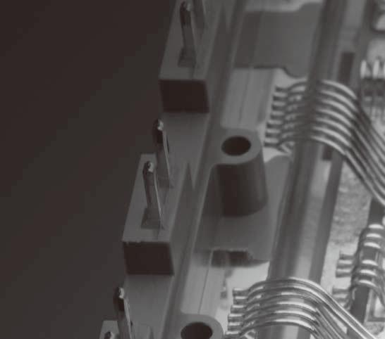
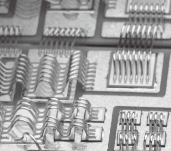


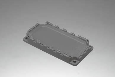

51
52
53 Overseas Subsidiaries America Fuji Electric Corp. of America Sales of electrical machinery and equipment, semiconductor devices, drive control equipment, and devices Tel URL Fuji Electric Brazil-Equipamentos de Energia Ltda * Sales of inverters, semiconductors, and power distribution Tel URL Asia Fuji Electric Asia Pacific Pte. Ltd. Sales of electrical distribution and control equipment, drive control equipment, and semiconductor devices Tel URL ces/fap.html Fuji Electric (Thailand) Co., Ltd. * Sales and engineering of electric substation equipment, control panels, and other electric equipment Tel Fuji Electric Power Supply (Thailand) Co., Ltd. Manufacture and sales of small- to medium-size UPS and internal power supplies Tel Fuji Electric Vietnam Co.,Ltd. Sales of electrical distribution and control equipment and drive control equipment Tel Fuji Furukawa E&C (Vietnam) Co., Ltd. * Engineering and construction of mechanics and electrical works Tel PT Fuji Electric Indonesia * Sales of inverters, servos, UPS, tools, and other component products Tel Fuji Electric India Pvt. Ltd. * Sales of drive control equipment and semiconductor devices Tel URL Fuji Electric Philippines, Inc. Manufacture of semiconductor devices Tel * Non-consolidated subsidiaries Fuji Electric Semiconductor (Malaysia) Sdn. Bhd. Manufacture of semiconductor devices Tel URL Fuji Electric (Malaysia) Sdn. Bhd. Manufacture of magnetic disk and aluminum substrate for magnetic disk Tel URL Fuji Furukawa E&C (Malaysia) Sdn. Bhd. * Engineering and construction of mechanics and electrical works Tel Fuji Electric Taiwan Co., Ltd. Sales of semiconductor devices, electrical distribution and control equipment, and drive control equipment Tel Fuji Electric Korea Co., Ltd. Sales of power distribution and control equipment, drive control equipment, rotators, high-voltage inverters, electronic control panels, mediumand large-sized UPS, and measurement equipment Tel URL Fuji Electric Middle East Branch Office Promotion of electrical products for the electrical utilities and the industrial plants Tel Europe Fuji Electric Europe GmbH Sales of electrical/electronic machinery and components Tel URL ces/fee.html Fuji Electric France S.A.S Manufacture and sales of measurement and control devices Tel URL China Fuji Electric (China) Co., Ltd. Sales of locally manufactured or imported products in China, and export of locally manufactured products Tel URL Shanghai Fuji Electric Switchgear Co., Ltd. Manufacture and sales of switching equipment, monitoring control appliances, and related facilities and products Tel URL Shanghai Fuji Electric Transformer Co., Ltd. Manufacture and sales of molded case transformers Tel URL Wuxi Fuji Electric FA Co., Ltd. Manufacture and sales of low/high-voltage inverters, temperature controllers, gas analyzers, and UPS Tel Fuji Electric (Changshu) Co., Ltd. Manufacture and sales of electromagnetic contactors and thermal relays Tel URL Fuji Electric (Zhuhai) Co., Ltd. Manufacture and sales of industrial electric heating devices Tel Fuji Electric (Shenzhen) Co., Ltd. Manufacture and sales of photoconductors and semiconductor devices Tel URL Fuji Electric Dalian Co., Ltd. Manufacture of low-voltage circuit breakers Tel Fuji Electric Motor (Dalian) Co., Ltd. Manufacture of industrial motors Tel Dailan Fuji Bingshan Vending Machine Co.,Ltd. Development, manufacture, sales, servicing, overhauling, and installation of vending machines, and related consulting Tel Fuji Electric (Hangzhou) Software Co., Ltd. Development of vending machine-related control software and development of management software Tel URL Zhejiang Innovation Fuji Technology Co., Ltd. * Design, development, and services pertaining to software Tel URL Fuji Electric FA (Asia) Co., Ltd. Sales of electrical distribution and control equipments Tel URL Fuji Electric Hong Kong Co., Ltd. Sales of semiconductor devices and photoconductors Tel URL Hoei Hong Kong Co., Ltd. Sales of electrical/electronic components Tel URL

54 Printed on recycled paper
All-SiC Modules Equipped with SiC Trench Gate MOSFETs
 All-SiC Modules Equipped with SiC Trench Gate MOSFETs NAKAZAWA, Masayoshi * DAICHO, Norihiro * TSUJI, Takashi * A B S T R A C T There are increasing expectations placed on products that utilize SiC modules
High-power IGBT Modules
 High-power IGBT Modules Takashi Nishimura Yoshikazu Takamiya Osamu Nakajima 1. Introduction To help curb global warming, clean energy, rather than fossil fuels, has been used increasingly in recent years.
High Power IGBT Module for Three-level Inverter
 High Power IGBT Module for Three-level Inverter Takashi Nishimura Takatoshi Kobayashi Yoshitaka Nishimura ABSTRACT In recent years, power conversion equipment used in the field of new energy and the field
(a) All-SiC 2-in-1 module
 All-SiC 2-in-1 module") All-SiC -in- Module CHONABAYASHI, Mikiya * OTOMO, Yoshinori * KARASAWA, Tatsuya * A B S T R A C T Fuji Electric has developed an utilizing a SiC device that has been adopted in the development of a high-performance
All-SiC -in- Module CHONABAYASHI, Mikiya * OTOMO, Yoshinori * KARASAWA, Tatsuya * A B S T R A C T Fuji Electric has developed an utilizing a SiC device that has been adopted in the development of a high-performance
PrimePACK of 7th-Generation X Series 1,700-V IGBT Modules
 PrimePACK of 7th-Generation 1,7-V IGBT Modules YAMAMOTO, Takuya * YOSHIWATARI, Shinichi * OKAMOTO, Yujin * A B S T R A C T The demand for large-capacity IGBT modules has been expanding for power conversion
Power Semiconductors Contributing in Energy Management
 Whole Number 247, ISSN 429-8284 4 214 Vol.6 No. Power Semiconductors Contributing in Energy Management 214 Vol.6 No. 4 Power Semiconductors Contributing in Energy Management Toward establishing low carbon
7th-Generation X Series RC-IGBT Module Line-Up for Industrial Applications
 7th-Generation X Series RC-IGBT Module Line-Up for Industrial Applications YAMANO, Akio * TAKASAKI, Aiko * ICHIKAWA, Hiroaki * A B S T R A C T In order to meet the market demand of the smaller size, lower
Fuji SiC Hybrid Module Application Note
 Fuji SiC Hybrid Module Application Note Fuji Electric Co., Ltd Aug. 2017 1 SiC Hybrid Module Application Note Chapter 1 Concept and Features Table of Contents Page 1 Basic concept 2 2 Features 3 3 Switching
V-Series Intelligent Power Modules
 V-Series Intelligent Power Modules Naoki Shimizu Hideaki Takahashi Keishirou Kumada A B S T R A C T Fuji Electric has developed a series of intelligent power modules for industrial applications, known
U-series IGBT Modules (1,700 V)
") U-series IGBT Modules (1,7 ) Yasuyuki Hoshi Yasushi Miyasaka Kentarou Muramatsu 1. Introduction In recent years, requirements have increased for high power semiconductor devices used in high power converters
U-series IGBT Modules (1,7 ) Yasuyuki Hoshi Yasushi Miyasaka Kentarou Muramatsu 1. Introduction In recent years, requirements have increased for high power semiconductor devices used in high power converters
T-series and U-series IGBT Modules (600 V)
") T-series and U-series IGBT Modules (6 V) Seiji Momota Syuuji Miyashita Hiroki Wakimoto 1. Introduction The IGBT (insulated gate bipolar transistor) module is the most popular power device in power electronics
T-series and U-series IGBT Modules (6 V) Seiji Momota Syuuji Miyashita Hiroki Wakimoto 1. Introduction The IGBT (insulated gate bipolar transistor) module is the most popular power device in power electronics
SiC Hybrid Module Application Note Chapter 2 Precautions for Use
 SiC Hybrid Module Application Note Chapter 2 Precautions for Use Table of contents Page 1 Maximum junction temperature 2 2 Short-circuit protection 3 3 Over voltage protection and safe operating area 4
Hybrid Si-SiC Modules for High Frequency Industrial Applications
 Hybrid Si-SiC Modules for High Frequency Industrial Applications ABSTRACT This presentation introduces a new family of 1200V IGBT modules that combine high switching frequency optimized silicon IGBTs with
New 1700V IGBT Modules with CSTBT and Improved FWDi
 New 17V IGBT Modules with CSTBT and Improved FWDi John Donlon 1, Eric Motto 1, Shinichi Iura 2, Eisuke Suekawa 2, Kazuhiro Morishita 3, Masuo Koga 3 1) Powerex Inc., Youngwood, PA, USA 2) Power Device
Sixth-Generation V-Series IGBT Module Application Note Chapter 1 Basic Concept and Features
 Sixth-Generation V-Series IGBT Module Application Note Chapter 1 Basic Concept and Features Table of contents Page 1 Basic concept of V series 1-2 2 Transition of device structure 1-3 3 Characteristics
Power Semiconductor contributing in energy and environment region
 ISSN 0429-8284 Whole Number 229 Power Semiconductor contributing in energy and environment region Power Semiconductor contributing in energy and environment region CONTENTS The Current Status and Future
2nd-Generation Low Loss SJ-MOSFET with Built-In Fast Diode Super J MOS S2FD Series
 2nd-Generation Low Loss SJ-MOSFET with Built-In Fast Diode Super J MOS WATANABE, Sota * SAKATA, Toshiaki * YAMASHITA, Chiho * A B S T R A C T In order to make efficient use of energy, there has been increasing
Efficiency improvement with silicon carbide based power modules
 Efficiency improvement with silicon carbide based power modules Zhang Xi*, Daniel Domes*, Roland Rupp** * Infineon Technologies AG, Max-Planck-Straße 5, 59581 Warstein, Germany ** Infineon Technologies
USING F-SERIES IGBT MODULES
 .0 Introduction Mitsubishi s new F-series IGBTs represent a significant advance over previous IGBT generations in terms of total power losses. The device remains fundamentally the same as a conventional
Simulation Technology for Power Electronics Equipment
 Simulation Technology for Power Electronics Equipment MATSUMOTO, Hiroyuki TAMATE, Michio YOSHIKAWA, Ko ABSTRACT As there is increasing demand for higher effi ciency and power density of the power electronics
1200 V SiC Super Junction Transistors operating at 250 C with extremely low energy losses for power conversion applications
 1200 V SiC Super Junction Transistors operating at 250 C with extremely low energy losses for power conversion applications Ranbir Singh, Siddarth Sundaresan, Eric Lieser and Michael Digangi GeneSiC Semiconductor,
Chapter 2. Technical Terms and Characteristics
 Chapter 2 Technical Terms and Characteristics CONTENTS Page 1 IGBT terms 2-2 2 IGBT characteristics 2-5 This section explains relevant technical terms and characteristics of IGBT modules. 2-1 1 IGBT terms
Some Key Researches on SiC Device Technologies and their Predicted Advantages
 18 POWER SEMICONDUCTORS www.mitsubishichips.com Some Key Researches on SiC Device Technologies and their Predicted Advantages SiC has proven to be a good candidate as a material for next generation power
Numerical study on very high speed silicon PiN diode possibility for power ICs in comparison with SiC-SBD
 Numerical study on very high speed silicon PiN diode possibility for power ICs in comparison with SiC-SBD Kenichi Takahama and Ichiro Omura Kyushu Institute of Technology Senshui-cho 1-1, Tobata-ku, Kitakyushu
The Next Generation of Power Conversion Systems Enabled by SiC Power Devices
 Innovations Embedded The Next Generation of Power Conversion Systems Enabled by SiC Power Devices White Paper The world has benefitted from technology innovations and continued advancements that have contributed
14 POWER MODULES
 14 POWER MODULES www.mitsubishichips.com Wide Temperature Operating Range of High Isolation HV-IGBT Modules Mitsubishi Electric has developed new High Voltage Insulated Gate Bipolar Transistor (HV-IGBT)
Chapter 1. Product Outline
 Chapter 1 Product Outline Contents Page 1. Introduction... 1-2 2. Product line-up... 1-4 3. Definition of type name and marking spec... 1-5 4. Package outline dimensions... 1-6 5. Absolute maximum ratings...
This chapter describes precautions for actual operation of the IGBT module.
 Chapter 5 Precautions for Use 1. Maximum Junction Temperature T vj(max) 5-2 2. Short-Circuit Protection 5-2 3. Over Voltage Protection and Safety Operation Area 5-2 4. Operation Condition and Dead time
New Power MOSFET. 1. Introduction. 2. Application of Power MOSFETs. Naoto Fujisawa Toshihiro Arai Tadanori Yamada
 New Power MOSFET Naoto Fujisawa Toshihiro Arai Tadanori Yamada 1. Introduction Due to the finer patterns and higher integration of LSIs, functions that were used a few years ago in minicomputers have now
10-PZ126PA080ME-M909F18Y. Maximum Ratings
 flow3xphase-sic 12V/8mΩ Features SiC-Power MOSFET s and Schottky Diodes 3 phase inverter topology with split output Improved switching behavior (reduced turn on energy and X-conduction) Ultra Low Inductance
Application Note. 3-Level Modules with Authentic RB-IGBT. Version 1.3
 Application Note 3-Level Modules with Authentic RB-IGBT Version 1.3 1 Content 1. Introduction... 2 2. Basics of T-type IGBT modules... 3 3. Characteristics of authentic RB-IGBT... 5 4. Leakage current
U-series IGBT Modules (1,200 V)
") U-series IGBT Modules (1, V) Yuichi Onozawa Shinichi Yoshiwatari Masahito Otsuki 1. Introduction Power conversion equiment such as general-use inverters and uninterrutible ower sulies (UPSs) is continuously
U-series IGBT Modules (1, V) Yuichi Onozawa Shinichi Yoshiwatari Masahito Otsuki 1. Introduction Power conversion equiment such as general-use inverters and uninterrutible ower sulies (UPSs) is continuously
Item Symbol Condition Rat ing Unit Collector-Emitter voltage Gate-Emitter voltage. Continuous. A Collector current
 7MBRS6 IGBT Modules IGBT MODULE (S series) 6 / / PIM Features Low CE(sat) Compact package P.C. board mount Converter diode bridge, Dynamic brake circuit pplications Inverter for motor drive C and DC servo
High Efficiency Power Conversion Using a Matrix Converter
 High Efficiency Power Conversion Using a Converter Jun-ichi Itoh Akihiro Odaka Ikuya Sato 1. Introduction As demands for energy savings have increased in recent years, inverters are being used in a wider
High Reliability Power MOSFETs for Space Applications
 High Reliability Power MOSFETs for Space Applications Masanori Inoue Takashi Kobayashi Atsushi Maruyama A B S T R A C T We have developed highly reliable and radiation-hardened power MOSFETs for use in
Temperature-Dependent Characterization of SiC Power Electronic Devices
 Temperature-Dependent Characterization of SiC Power Electronic Devices Madhu Sudhan Chinthavali 1 chinthavalim@ornl.gov Burak Ozpineci 2 burak@ieee.org Leon M. Tolbert 2, 3 tolbert@utk.edu 1 Oak Ridge
Item Symbol Condition Rating Unit Collector-Emitter voltage Gate-Emitter voltage. A Collector current A. Continuous Tc=25 C 35. Tc=80 C 30.
 7MBR2S12 IGBT Modules IGBT MODULE (S series) 12 / 2 / PIM Features Low CE(sat) Compact package P.C. board mount Converter diode bridge, Dynamic brake circuit pplications Inverter for motor drive C and
Features TO-264 E. Symbol Description SGL50N60RUFD Units V CES Collector-Emitter Voltage 600 V V GES Gate-Emitter Voltage ± 20 V Collector T
 Short Circuit Rated IGBT General Description Fairchild's RUFD series of Insulated Gate Bipolar Transistors (IGBTs) provide low conduction and switching losses as well as short circuit ruggedness. The RUFD
Fuji 7th Generation IGBT Module X Series Application Manual. Apr., 2018 Rev.1.0. Fuji Electric Co., Ltd. All rights reserved.
 Fuji 7th Generation IGBT Module X Series Application Manual Apr., 218 Rev.1. MT5F3673 Fuji Electric Co., Ltd. All rights reserved. Warning: This manual contains the product specifications, characteristics,
ELECTRONIC DEVICES AND CIRCUITS
 ELECTRONIC DEVICES AND CIRCUITS 1. At room temperature the current in an intrinsic semiconductor is due to A. holes B. electrons C. ions D. holes and electrons 2. Work function is the maximum energy required
IGBT STARPOWER SEMICONDUCTOR TM. Molding Type Module. 1200V/10A PIM in one-package. General Description. Features. Typical Applications
 STRPOWER SEMICONDUCTOR TM IGBT GD10PJK120L1S Preliminary Molding Type Module 1200/10 PIM in one-package General Description STRPOWER IGBT Power Module provides ultra low conduction and switching loss as
2016 Vol.62 No. Power Semiconductors Contributing in Energy Management
 4 216 Vol.62 No. Power Semiconductors Contributing in Energy Management 216 Vol.62 No. 4 Power Semiconductors Contributing in Energy Management Cover Photo (clockwise from the upper left): FUJI ELECTRIC
Investigation of Parasitic Turn-ON in Silicon IGBT and Silicon Carbide MOSFET Devices: A Technology Evaluation. Acknowledgements. Keywords.
 Investigation of Parasitic Turn-ON in Silicon IGBT and Silicon Carbide MOSFET Devices: A Technology Evaluation Saeed Jahdi, Olayiwola Alatise, Jose Ortiz-Gonzalez, Peter Gammon, Li Ran and Phil Mawby School
APPLICATION NOTE ANxxxx. Understanding the Datasheet of a SiC Power Schottky Diode
 APPLICATION NOTE ANxxxx CONTENTS 1 Introduction 1 2 Nomenclature 1 3 Absolute Maximum Ratings 2 4 Electrical Characteristics 5 5 Thermal / Mechanical Characteristics 7 6 Typical Performance Curves 8 7
4H-SiC V-Groove Trench MOSFETs with the Buried p + Regions
 ELECTRONICS 4H-SiC V-Groove Trench MOSFETs with the Buried p + Regions Yu SAITOH*, Toru HIYOSHI, Keiji WADA, Takeyoshi MASUDA, Takashi TSUNO and Yasuki MIKAMURA ----------------------------------------------------------------------------------------------------------------------------------------------------------------------------------------------------------------------------------------------------------
IGBTs (Insulated Gate Bipolar Transistor)
") IGBTs (Insulated Gate Bipolar Transistor) Description This document describes the basic structures, ratings, and electrical characteristics of IGBTs. It also provides usage considerations for IGBTs. 1
IGBTs (Insulated Gate Bipolar Transistor) Description This document describes the basic structures, ratings, and electrical characteristics of IGBTs. It also provides usage considerations for IGBTs. 1
Item Symbol Condition Rat ing Unit Collector-Emitter voltage Gate-Emitter voltage. Continuous. A Collector current
 7MBR3S6 IGBT Modules IGBT MODULE (S series) 6 / 3 / PIM Features Low CE(sat) Compact package P.C. board mount Converter diode bridge, Dynamic brake circuit pplications Inverter for motor drive C and DC
Symbol Description GD200CLT120C2S Units V CES Collector-Emitter Voltage 1200 V V GES Gate-Emitter Voltage ±20V V
 STARPOWER SEMICONDUCTOR TM IGBT Preliminary Molding Type Module 1200V/200A 2 in one-package General Description STARPOWER IGBT Power Module provides ultra low conduction loss as well as short circuit ruggedness.
MBN3600E17F Silicon N-channel IGBT 1700V F version
 Silicon N-channel IGBT 17V F version Spec.No.IGBT-SP-124 R P1 FEATURES Soft switching behavior & low conduction loss: Soft low-injection punch-through with trench gate IGBT. Low driving power: Low input
IGB03N120H2. HighSpeed 2-Technology. Power Semiconductors 1 Rev. 2.4 Oct. 07
 HighSpeed 2-Technology Designed for frequency inverters for washing machines, fans, pumps and vacuum cleaners 2 nd generation HighSpeed-Technology for 1200V applications offers: - loss reduction in resonant
Symbol Parameter Typical
 PRODUCT SUMMARY (TYPICAL) V DS (V) 600 R DS(on) ( ) 0.29 Q rr (nc) 29 Features Low Q rr Free-wheeling diode not required Low-side Quiet Tab for reduced EMI RoHS compliant High frequency operation Applications
Development of 13-V, 5000-A DC Power Supply with High-Frequency Transformer Coupling Applied to Electric Furnace
 Development of 13-V, 5-A DC Power Supply with High-Frequency Transformer Coupling Applied to Electric Furnace Toshihiko Noguchi, Senior Member, Kosuke Nishiyama Department of Electric, Electronics, and
IGBT STARPOWER GD400SGK120C2S. Absolute Maximum Ratings T C =25 unless otherwise noted SEMICONDUCTOR TM. Molding Type Module
 STARPOWER SEMICONDUCTOR TM IGBT GD400SGK120C2S Molding Type Module 1200V/400A 1 in one-package General Description STARPOWER IGBT Power Module provides ultra low conduction and switching loss as well as
D AB Z DETAIL "B" DETAIL "A"
 QID1215 Preliminary Powerex, Inc., 173 Pavilion Lane, Youngwood, Pennsylvania 15697 (72) 925-7272 www.pwrx.com Split Dual Si/SiC Hybrid IGBT Module 1 Amperes/12 Volts Y A AA F D AB Z AC Q DETAIL "B" Q
Effects of the Internal Layout on the Performance of IGBT Power Modules
 Effects of the Internal Layout on the Performance of IGBT Power Modules A. Consoli, F. Gennaro Dept. of Electrical, Electronic and System Engineering University of Catania Viale A. Doria, 6 I-95125 Catania
MG200Q2YS60A(1200V/200A 2in1)
") TOSHIBA IGBT Module Silicon N Channel IGBT (V/A in) High Power Switching Applications Motor Control Applications Integrates a complete half bridge power circuit and fault-signal output circuit in one package.
TOSHIBA IGBT Module Silicon N Channel IGBT (V/A in) High Power Switching Applications Motor Control Applications Integrates a complete half bridge power circuit and fault-signal output circuit in one package.
Raffael Schnell, Product Manager, ABB Switzerland Ltd, Semiconductors LinPak a new low inductive phase-leg IGBT module ABB
 Raffael Schnell, Product Manager, ABB Switzerland Ltd, Semiconductors LinPak a new low inductive phase-leg IGBT module Slide 1 The LinPak Main features Low inductive target inductance 1 nh, ready for fast
Symbol Parameters Test Conditions Min Typ Max Unit R thjc. Per IGBT 0.09 K/W R thjcd
 2V 2A IGBT Module RoHS Features Ultra low loss High ruggedness High short circuit capability Positive temperature coefficient With fast free-wheeling diodes Agency Approvals Applications Inverter Converter
Symbol Parameter Typical
 PRODUCT SUMMARY (TYPICAL) V DS (V) 650 R DS(on) (m ) 110 Q rr (nc) 54 Features Low Q rr Free-wheeling diode not required Low-side Quiet Tab for reduced EMI RoHS compliant High frequency operation Applications
Item Symbol Condition Rating Unit Collector-Emitter voltage Gate-Emitter voltage. A Collector current A. Continuous Tc=25 C 35. Tc=75 C 30.
 7MBRS14 IGBT Modules IGBT MODULE (S series) 14 / / PIM Features Low CE(sat) Compact Package P.C. Board Mount Module Converter Diode Bridge Dynamic Brake Circuit pplications Inverter for Motoe Drive C and
IGBT STARPOWER SEMICONDUCTOR TM. Molding Type Module. 1200V/225A 6 in one-package. General Description. Features. Typical Applications
 STARPOWER SEMICONDUCTOR TM IGBT GD225HTL120C7S Preliminary Molding Type Module 1200V/225A 6 in one-package General Description STARPOWER IGBT power module provides ultra low conduction loss as well as
Chapter 1. Product Outline
 Chapter 1 Product Outline Contents Page 1. Introduction... 1-2 2. Product line-up... 1-4 3. Definition of Type Name and Marking Spec... 1-5 4. Package outline dimensions... 1-6 5. bsolute Maximum Ratings...
Item Symbol Condition Rat ing Unit Collector-Emitter voltage Gate-Emitter voltage. Continuous Tc=25 C 75. A Collector current.
 7MBR5SB12 IGBT Modules IGBT MODULE (S series) 12 / 5 / PIM Features Low CE(sat) Compact package P.C. board mount Converter diode bridge, Dynamic brake circuit pplications Inverter for motor drive C and
Power Matters Microsemi SiC Products
 Microsemi SiC Products James Kerr Director of Marketing Power Discrete Products Microsemi Power Products MOSFETs (100V-1200V) Highest Performance SiC MOSFETs 1200V MOSFETs FREDFETs (MOSFET with fast body
Sixth-Generation V-Series IGBT Module Application Note Chapter 1 Basic Concept and Features
 Sixth-Generation V-Series IGBT Module Application Note Chapter 1 Basic Concept and Features Table of contents Page 1 Basic concept of V series 1-2 2 Transition of device structure 1-3 3 Characteristics
Collector-Emitter voltage VCES 1200 V Gate-Emitter voltage VGES ±20 V Ic Continuous Tc=100 C 50
 IGBT MODULE (V series) 12V / A / PIM Features Low VCE(sat) Compact Package P.C.Board Mount Module Converter Diode Bridge Dynamic Brake Circuit RoHS compliant product Applications Inverter for Motor Drive
Study of Static and Dynamic Characteristics of Silicon and Silicon Carbide Devices
 Study of Static and Dynamic Characteristics of Silicon and Silicon Carbide Devices Sreenath S Dept. of Electrical & Electronics Engineering Manipal University Jaipur Jaipur, India P. Ganesan External Guide
The Quest for High Power Density
 The Quest for High Power Density Welcome to the GaN Era Power Conversion Technology Drivers Key design objectives across all applications: High power density High efficiency High reliability Low cost 2
Data Sheet GHIS040A060S A2
 Buck Chopper with Field Stop Trench IGBT + SiC SBD V CES =600V I C = 40A @T C = 100 0 C Features Field StopTrench Fast IGBT Low voltage drop Low tail current Switching frequency up to 50 khz Low leakage
NXH80T120L2Q0S2G/S2TG, NXH80T120L2Q0P2G. Q0PACK Module
 NXH8T2L2QS2G/S2TG, NXH8T2L2QP2G QPACK Module The NXH8T2L2QS2/P2G is a power module containing a T type neutral point clamped (NPC) three level inverter stage. The integrated field stop trench IGBTs and
High voltage and large current dynamic test of SiC diodes and hybrid module
 International Conference on Manufacturing Science and Engineering (ICMSE 2015) High voltage and large current dynamic test of SiC diodes and hybrid module Ao Liu 1, a *, Gang Chen1, 2, Song Bai1, 2, Run
SuperLLD3 Series of 600 V Low-loss Fast-recovery Diodes
 SuperLLD3 Series of V Low-loss Fast-recovery Diodes Tetsuhiro Morimoto Taketo Watashima Masaki Ichinose 1. Introduction At present, societal problems such as global warming and environmental disruption
Power Electronics Power semiconductor devices. Dr. Firas Obeidat
 Power Electronics Power semiconductor devices Dr. Firas Obeidat 1 Table of contents 1 Introduction 2 Classifications of Power Switches 3 Power Diodes 4 Thyristors (SCRs) 5 The Triac 6 The Gate Turn-Off
Item Symbol Condition Rating Unit Collector-Emitter voltage Gate-Emitter voltage. A Collector current. Tc=80 C 35. 1ms IC -IC pulse.
 7MBR5U12 IGBT Modules IGBT MODULE (U series) 12 / 5 / PIM Features Low CE(sat) Compact Package P.C. Board Mount Module Converter Diode Bridge Dynamic Brake Circuit pplications Inverter for Motoe Drive
Università degli Studi di Roma Tor Vergata Dipartimento di Ingegneria Elettronica. Analogue Electronics. Paolo Colantonio A.A.
 Università degli Studi di Roma Tor Vergata Dipartimento di Ingegneria Elettronica Analogue Electronics Paolo Colantonio A.A. 2015-16 Introduction: materials Conductors e.g. copper or aluminum have a cloud
A new compact power modules range for efficient solar inverters
 A new compact power modules range for efficient solar inverters Serge Bontemps, Pierre-Laurent Doumergue Microsemi PPG power module Products, Chemin de Magret, F-33700 Merignac Abstract The decrease of
Molding Type Module IGBT, 2-in-1 Package, 1200 V and 300 A
 Molding Type Module IGBT, 2-in-1 Package, 12 V and 3 A VS-GB3TH12N Double INT-A-PAK FEATURES 1 μs short circuit capability V CE(on) with positive temperature coefficient Maximum junction temperature 15
GS66516T Top-side cooled 650 V E-mode GaN transistor Preliminary Datasheet
 Features 650 V enhancement mode power switch Top-side cooled configuration R DS(on) = 25 mω I DS(max) = 60 A Ultra-low FOM Island Technology die Low inductance GaNPX package Easy gate drive requirements
V CE = 650 V, I C = 30 A Trench Field Stop IGBTs with Fast Recovery Diode KGF65A3L, MGF65A3L, FGF65A3L. Package
 V CE = 65 V, I C = 3 A Trench Field Stop IGBTs with Fast Recovery Diode Data Sheet Description Package KGF65A3L, MGF65A3L, and FGF65A3L are 65 V Field Stop IGBTs. Sanken original trench structure decreases
CP15TD1-24A. DIP-CIB 3Ø Converter + 3Ø Inverter + Brake 15 Amperes/1200 Volts
 Outline Drawing and Circuit Diagram Dimensions Inches Millimeters A 2.68±.1 68.±.3 B 1.73±.2 44.±.5 C.58±.4 14.7±.1 D 3.1±.2 79.±.5 E 2.83 72. F.16±.1 4.±.3 G 2.83±.1 72.±.3 H.7 2. J.2±.8 5.±.2 K.87 22.
Introduction. Figure 2: The HiPak standard (left) and high-insulation (right) modules with 3300V SPT + IGBT technology.
 and high-insulation (right) modules with 3300V SPT + IGBT technology.") M. Rahimo, U. Schlapbach, A. Kopta, R. Schnell, S. Linder ABB Switzerland Ltd, Semiconductors, Fabrikstrasse 3, CH 5600 Lenzburg, Switzerland email: munaf.rahimo@ch.abb.com Abstract: Following the successful
M. Rahimo, U. Schlapbach, A. Kopta, R. Schnell, S. Linder ABB Switzerland Ltd, Semiconductors, Fabrikstrasse 3, CH 5600 Lenzburg, Switzerland email: munaf.rahimo@ch.abb.com Abstract: Following the successful
Collector-Emitter voltage VCES 600 V Gate-Emitter voltage VGES ±20 V Ic Continuous Tc=80 C 100
 7MBRVP65 IGBT MODULE (V series) 6V / A / PIM Features Low VCE(sat) Compact Package P.C.Board Mount Module Converter Diode Bridge Dynamic Brake Circuit RoHS compliant product Applications Inverter for Motor
DIM600XSM45-F000. Single Switch IGBT Module FEATURES KEY PARAMETERS V CES. 4500V V CE(sat) * (typ) 2.9 V I C
 * (typ) 2.9 V I C") Single Switch IGBT Module DS5874-1.1 August 26 (LN24724) FEATURES 1µs Short Circuit Withstand Soft Punch Through Silicon Lead Free construction Isolated MMC Base with AlN Substrates High Thermal Cycling
Single Switch IGBT Module DS5874-1.1 August 26 (LN24724) FEATURES 1µs Short Circuit Withstand Soft Punch Through Silicon Lead Free construction Isolated MMC Base with AlN Substrates High Thermal Cycling
Data Sheet GHIS030A120S-A2
 Buck Chopper with Field Stop Trench IGBT + SiC SBD V CES =1200V I C = 30A @T C = 100 0 C E A G C Features Field StopTrench Fast IGBT - Low voltage drop - Low tail current - Switching frequency up to 50
V (4TYP) U (5TYP) V 0.28 Dia. 7.0 Dia.
 U (5TYP) V 0.28 Dia. 7.0 Dia.") QIC68 Preliminary Powerex, Inc., 73 Pavilion Lane, Youngwood, Pennsylvania 697 (724) 9-7272 www.pwrx.com Dual Common Emitter HVIGBT Module 8 Amperes/6 Volts S NUTS (3TYP) F A D F J (2TYP) C N 7 8 H B E
QIC68 Preliminary Powerex, Inc., 73 Pavilion Lane, Youngwood, Pennsylvania 697 (724) 9-7272 www.pwrx.com Dual Common Emitter HVIGBT Module 8 Amperes/6 Volts S NUTS (3TYP) F A D F J (2TYP) C N 7 8 H B E
TEPZZ Z 98 _A_T EP A1 (19) (11) EP A1. (12) EUROPEAN PATENT APPLICATION published in accordance with Art.
 (11) EP A1. (12) EUROPEAN PATENT APPLICATION published in accordance with Art.") (19) TEPZZ Z 98 _A_T (11) EP 3 029 821 A1 (12) EUROPEAN PATENT APPLICATION published in accordance with Art. 153(4) EPC (43) Date of publication: 08.06.2016 Bulletin 2016/23 (21) Application number: 14831328.1
(19) TEPZZ Z 98 _A_T (11) EP 3 029 821 A1 (12) EUROPEAN PATENT APPLICATION published in accordance with Art. 153(4) EPC (43) Date of publication: 08.06.2016 Bulletin 2016/23 (21) Application number: 14831328.1
Ic Continuous Tc=80 C 35 Icp 1ms Tc=80 C 70 -Ic 35 -Ic pulse 1ms 70 Collector power dissipation Pc 1 device 210 W
 7MBR35VP15 IGBT MODULE (V series) 1V / 5A / PIM Features Low VCE(sat) Compact Package P.C.Board Mount Module Converter Diode Bridge Dynamic Brake Circuit RoHS compliant product Applications Inverter for
GS61008P Bottom-side cooled 100 V E-mode GaN transistor Preliminary Datasheet
 Features 100 V enhancement mode power switch Bottom-side cooled configuration R DS(on) = 7 mω I DS(max) = 90 A Ultra-low FOM Island Technology die Low inductance GaNPX package Easy gate drive requirements
Abstract: Following fast on the successful market introduction of the 1200V Soft-Punch-Through. 1. Introduction
 Novel Soft-Punch-Through (SPT) 1700V IGBT Sets Benchmark on Technology Curve M. Rahimo, W. Lukasch *, C. von Arx, A. Kopta, R. Schnell, S. Dewar, S. Linder ABB Semiconductors AG, Lenzburg, Switzerland
MG400V2YS60A MG400V2YS60A. High Power Switching Applications Motor Control Applications. Equivalent Circuit
 MGV2YS6A TOSHIBA IGBT Module Silicon N Channel IGBT MGV2YS6A High Power Switching Applications Motor Control Applications Unit in mm The electrodes are isolated from case. Enhancement mode Thermal output
IGBT Module Chip Improvements for Industrial Motor Drives
 IGBT Module Chip Improvements for Industrial Motor Drives John F. Donlon Powerex, Inc. 173 Pavilion Lane Youngwood, PA USA Katsumi Satoh Mitsubishi Electric Corporation Power Semiconductor Device Works
Fundamentals of Power Semiconductor Devices
 В. Jayant Baliga Fundamentals of Power Semiconductor Devices 4y Spri ringer Contents Preface vii Chapter 1 Introduction 1 1.1 Ideal and Typical Power Switching Waveforms 3 1.2 Ideal and Typical Power Device
GaN Based Power Conversion: Moving On! Tim McDonald APEC Key Component Technologies for Power Electronics in Electric Drive Vehicles
 1 GaN Based Power Conversion: Moving On! Key Component Technologies for Power Electronics in Electric Drive Vehicles Tim McDonald APEC 2013 2 Acknowledgements Collaborators: Tim McDonald (1), Han S. Lee
GS61004B 100V enhancement mode GaN transistor Preliminary Datasheet
 Features 100V enhancement mode power switch Bottom-side cooled configuration R DS(on) = 15 mω I DS(max) = 45 A Ultra-low FOM Island Technology die Low inductance GaNPX package Easy gate drive requirements
Semiconductors. Whole Number 209
 Semiconductors Whole Number 209 The key technology to power electronics, Fuji Electric, s power devices. The innovative technologies of Fuji Electric, s power devices lead to market needs. Our power devices
SJEP120R125. Silicon Carbide. Normally-OFF Trench Silicon Carbide Power JFET. Product Summary
 NormallyOFF Trench Power JFET Features: Compatible with Standard PWM ICs Positive Temperature Coefficient for Ease of Paralleling Temperature Independent Switching Behavior 175 C Maximum Operating Temperature
AN1387 APPLICATION NOTE APPLICATION OF A NEW MONOLITHIC SMART IGBT IN DC MOTOR CONTROL FOR HOME APPLIANCES
 AN1387 APPLICATION NOTE APPLICATION OF A NEW MONOLITHIC SMART IGBT IN DC MOTOR CONTROL FOR HOME APPLIANCES A. Alessandria - L. Fragapane - S. Musumeci 1. ABSTRACT This application notes aims to outline
Resonance Analysis Focusing on Stray Inductance and Capacitance of Laminated Bus Bars
 IEEJ Journal of Industry Applications Vol.5 No.6 pp.407 42 DOI: 0.54/ieejjia.5.407 Paper Resonance Analysis Focusing on Stray Inductance and Capacitance of Laminated Bus Bars Akihiro Hino Member, Keiji
Collector-Emitter voltage VCES 1200 V Gate-Emitter voltage VGES ±20 V Ic Continuous Tc=100 C 100
 6MBIVB125 IGBT MODULE (V series) 12V / A / 6 in one package Features Compact Package P.C.Board Mount Low VCE (sat) Applications Inverter for Motor Drive AC and DC Servo Drive Amplifier Uninterruptible
Molding Type Module IGBT, Chopper in 1 Package, 1200 V and 300 A
 Molding Type Module IGBT, Chopper in 1 Package, 12 V and 3 A VS-GB3NH12N PRIMARY CHARACTERISTICS V CES I C at T C = 8 C V CE(on) (typical) at I C = 3 A, 25 C Speed Package Circuit configuration Dual INT-A-PAK