100V ENHANCEMENT MODE HIGH ELECTRON MOBILITY TRANSISTOR (HEMT) Michele Rossitto. Marketing Director MOSFETs and Power ICs
|
|
|
- Christina Welch
- 5 years ago
- Views:
Transcription


1 100V ENHANCEMENT MODE HIGH ELECTRON MOBILITY TRANSISTOR (HEMT) Michele Rossitto Marketing Director MOSFETs and Power ICs
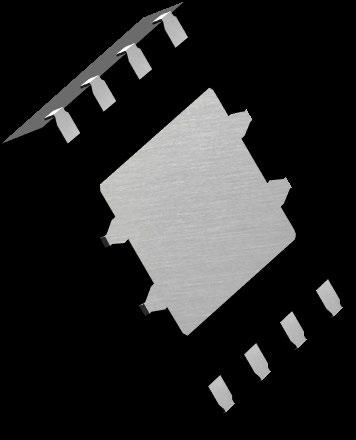
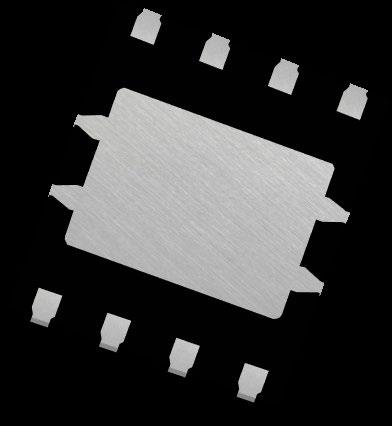
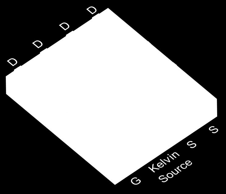
2 100V GaN in PowerPAK 6 x 5 mm² Package Enhancement Mode GaN Transistor Superior R DS -Q g FOM Re-workability Classic PowerPAK Construction Industry Low Q g Q g of 8 nc Built-in ESD Protective encapsulation For power supplies in telecom and servers Leadership C oss Clip bonding 6 mω FOM = 48 mω-nc
3 Vishay 100V egan Highlights emode Gan in industry standard 6 x 5 mm 2 PowerPAK Drop in replacement for existing Si package with minimal PCB modification. No special solder profile needed. Easy to inspect Clip bonded drain and source terminals resulting in low package impedances. Vishay proprietary ESD protection for the sensitive gate Kelvin source connection for clean gate drives 3 rd quadrant conduction without body diode Zero Q rr in synchronous modes of operation Low C oss related losses. Q oss / E oss are 21 nc / 0.4 uj Efficient operation at higher switching frequencies Low Q g of 8 nc. Q gs of 1 nc and near-zero Q gd Gate switching times of nsec even with modest gate drive Drastically reduces dead time and related 3 rd quadrant losses.

4 100V GaN in PowerPAK 6x5 mm² Package Excellent R DS -Q g FOM Increases Efficiency Enhancement mode device R DS -Q g FOM = 48 mω-nc 6 mω Clip construction allows high current handling 1 mm Optimized for Switching Applications Kelvin source connection reduces gate loop inductance to minimize ringing Industry low Q g and C oss Minimized Q rr prevents ringing Target Applications DC/DC converters Power supplies for mission critical applications Solar micro inverter Motor drive control Parameters SiR04G10D UNIT Package Dimension (mm x mm x mm) 6 x 5 x 1 mm x mm x mm V DS 100 V R V GS = 6V T J = 25 ºC 6 mω Q g 8 Q gs 0.3 nc Q gd 0.01 C oss 275 pf R DS -Q g FOM 48 mω-nc Sampling in 2019 Top View Bottom View Package Is Optimized for PCB Surface Mounting Encapsulated package is easier for rework Package dimension is identical to PowerPAK SO-8
5 Vishay 100V GaN vs. Competitors Top R DS -Q g FOM Optimized for switching applications Competitive R DS(ON) Reduces conduction loss 6 mω at V GS = 5V 16% lower R DS - C oss FOM Reduces loss from charging and discharging Q oss during ZVS intervals 90.0 R DS -Q g FOM (mω-nc) 8.0 Typical R DS(ON) (mω) 3500 R DS -C oss FOM (mω-pf) Vishay 100V GaN Competitor 1 Competitor Vishay 100V GaN Competitor 1 Competitor 2 0 Vishay 100V GaN Competitor 1 Competitor 2
 4 mω Q g = 72 nc FOM = 216 mω-nc Typ.")
 3.")
6 Technology Roadmap for 100V Products R DS -Q g FOM (mω-nc) SiR668ADP SiR668DP FOM = 288 mω-nc Typ. R DS(ON) 4 mω Q g = 72 nc FOM = 216 mω-nc Typ. R DS(ON) 4 mω Q g = 54 nc 20% improvement on Q g of 250M cell SG Roadmap of Silicon Conventional solutions with aggressive improvement; targeting mass market Roadmap of Wide Band Gap Revolutionary FOM for mission critical designs without concern of budget FOM = 125 mω-nc PowerPAK SO8 Typ. R DS(ON) 3.4 mω Q g = 35 nc Aims for leadership R DS -Q g FOM with low Q oss 100V e-gan PowerPAK 6 X 5 SiR04G10D FOM = 48 mω-nc Typ. R DS(ON) 6 mω Q g = 8 nc & Beyond

7 GaN vs Si in High Voltage Synchronous Buck Convertor 100V GaN benchmarked against best-in-class 100V silicon in a 48V à 12V synchronous buck convertor Both devices tested till they reached T j ~ 100 o C GaN tested to 500 khz. Silicon limited to 250 khz. Test set up designed to use GaN or silicon side by side under identical conditions Vin C in G D S SIR040G10D vs SiRA104DP 48Vin à 12V Sync Buck 3.3 uh 500 khz 250 khz 180W 150W D Vout G I S à D C out GND S GND 7

8 GaN vs Si Synchronous Buck Efficiency Even at 2x switching frequency GaN is more efficient Efficiency difference is more pronounced at light load Silicon has constant 4W power loss, arising from Qrr related losses Benefits of zero Qrr can be significant for high voltage synchronous buck and SSR applications. 8
9 V gsh and V gsl Comparison Drawn to different time scales 100 ns/div for GaN and 200 ns/div for Si Waveforms depict high side and low side gate voltages on no load and without any voltage on the DC bus Dead time set to 20 ns for both GaN has no crossover 20 ns. Low Qg can handle very short transition times for gate rise and fall. Reduces dead time requirements and body diode conduction loss With Si, 20 nsec dead time results in crossover of gate voltage and shoot through. 9
10 Gate Switching Times - GaN vs Silicon Si switches slowly and has shoot through under different conditions. All waveforms with common 20 nsec deadtime 10

11 In a synchronous buck LS MOSFET always conducts in 3 rd quadrant Turning OFF the LS is not an issue with GaN which has no body diode HS GaN can turn ON under 20 nsec without shoot through No diode reverse recovery time or losses! GaN vs Si Qrr Matters With silicon, body diode of the LS MOSFET must be hard commutated Reverse recovery time always gets added to the dead time Shoot through conditions exist as the HS MOSFET turns on Increased losses prevent higher frequency operation with silicon 11
12 THANK YOU! 12
HCS65R110FE (Fast Recovery Diode Type) 650V N-Channel Super Junction MOSFET
 650V N-Channel Super Junction MOSFET") HCS65R110FE (Fast Recovery Diode Type) 650V N-Channel Super Junction MOSFET Features Very Low FOM (R DS(on) X Q g ) Extremely low switching loss Excellent stability and uniformity 100% Avalanche Tested
HCS65R110FE (Fast Recovery Diode Type) 650V N-Channel Super Junction MOSFET Features Very Low FOM (R DS(on) X Q g ) Extremely low switching loss Excellent stability and uniformity 100% Avalanche Tested
Unlocking the Power of GaN PSMA Semiconductor Committee Industry Session
 Unlocking the Power of GaN PSMA Semiconductor Committee Industry Session March 24 th 2016 Dan Kinzer, COO/CTO dan.kinzer@navitassemi.com 1 Mobility (cm 2 /Vs) EBR Field (MV/cm) GaN vs. Si WBG GaN material
GaN Transistors for Efficient Power Conversion
 GaN Transistors for Efficient Power Conversion Agenda How GaN works Electrical Characteristics Design Basics Design Examples Summary 2 2 How GaN Works 3 3 The Ideal Power Switch Block Infinite Voltage
GaAs PowerStages for Very High Frequency Power Supplies. Greg Miller Sr. VP - Engineering Sarda Technologies
 GaAs PowerStages for Very High Frequency Power Supplies Greg Miller Sr. VP - Engineering Sarda Technologies gmiller@sardatech.com Agenda Case for Higher Power Density Voltage Regulators Limitations of
Switch mode power supplies Low gate charge. Power factor correction modules Low intrinsic capacitance
 Description United Silicon Carbide's cascode products co-package its highperformance F3 SiC fast JFETs with a cascode optimized MOSFET to produce the only standard gate drive SiC device in the market today.
GS66516T Top-side cooled 650 V E-mode GaN transistor Preliminary Datasheet
 Features 650 V enhancement mode power switch Top-side cooled configuration R DS(on) = 25 mω I DS(max) = 60 A Ultra-low FOM Island Technology die Low inductance GaNPX package Easy gate drive requirements
GS61004B 100V enhancement mode GaN transistor Preliminary Datasheet
 Features 100V enhancement mode power switch Bottom-side cooled configuration R DS(on) = 15 mω I DS(max) = 45 A Ultra-low FOM Island Technology die Low inductance GaNPX package Easy gate drive requirements
Introducing egan IC targeting Highly Resonant Wireless Power
 Dr. M. A. de Rooij The egan FET Journey Continues Introducing egan IC targeting Highly Resonant Wireless Power Efficient Power Conversion Corporation EPC - The Leader in egan FETs www.epc-co.com 1 Agenda
UF3C120080K4S. 1200V-80mW SiC Cascode DATASHEET. Description. Features. Typical applications CASE D (1) CASE G (4) KS (3) S (2) Rev.
 CASE G (4) KS (3) S (2) Rev.") 1V-8mW SiC Cascode Rev. A, January 19 DATASHEET UF3C18K4S CASE CASE D (1) Description United Silicon Carbide's cascode products co-package its highperformance F3 SiC fast JFETs with a cascode optimized
1V-8mW SiC Cascode Rev. A, January 19 DATASHEET UF3C18K4S CASE CASE D (1) Description United Silicon Carbide's cascode products co-package its highperformance F3 SiC fast JFETs with a cascode optimized
GaN is Crushing Silicon. EPC - The Leader in GaN Technology IEEE PELS
 GaN is Crushing Silicon EPC - The Leader in GaN Technology IEEE PELS 2014 www.epc-co.com 1 Agenda How egan FETs work Hard Switched DC-DC converters High Efficiency point-of-load converter Envelope Tracking
27mW - 650V SiC Cascode UJ3C065030K3S Datasheet. Description. Typical Applications. Maximum Ratings
 Description United Silicon Carbide's cascode products co-package its highperformance G3 SiC JFETs with a cascode optimized MOSFET to produce the only standard gate drive SiC device in the market today.
80mW - 650V SiC Cascode UJ3C065080K3S Datasheet. Description. Typical Applications. Maximum Ratings
 Description United Silicon Carbide's cascode products co-package its highperformance G3 SiC JFETs with a cascode optimized MOSFET to produce the only standard gate drive SiC device in the market today.
35mW V SiC Cascode UJ3C120040K3S Datasheet. Description. Typical Applications. Maximum Ratings
 Description United Silicon Carbide's cascode products co-package its highperformance G3 SiC JFETs with a cascode optimized MOSFET to produce the only standard gate drive SiC device in the market today.
235 W Maximum Power Dissipation (whole module) 470 T J Junction Operating Temperature -40 to 150. Torque strength
 470 T J Junction Operating Temperature -40 to 150. Torque strength") Discontinued PRODUCT SUMMARY (TYPICAL) V DS (V) 600 R DS(on) (m ) 30 GaN Power Hybrid HEMT Half-Bridge Module Features High frequency operation Free-wheeling diode not required Applications Compact DC-DC
Discontinued PRODUCT SUMMARY (TYPICAL) V DS (V) 600 R DS(on) (m ) 30 GaN Power Hybrid HEMT Half-Bridge Module Features High frequency operation Free-wheeling diode not required Applications Compact DC-DC
Performance Comparison for A4WP Class-3 Wireless Power Compliance between egan FET and MOSFET in a ZVS Class D Amplifier
 The egan FET Journey Continues Performance Comparison for A4WP Class-3 Wireless Power Compliance between egan FET and MOSFET in a ZVS Class D Amplifier EPC - The leader in GaN Technology www.epc-co.com
S2301 N-channel SiC power MOSFET bare die
 S23 N-channel SiC power MOSFET bare die V DSS R DS(on) (Typ.) I D 2V 8mW 4A* Features Inner circuit ) Low on-resistance (D) 2) Fast switching speed 3) Fast reverse recovery 4) Easy to parallel 5) Simple
GS61008T Top-side cooled 100 V E-mode GaN transistor Preliminary Datasheet
 Features 100 V enhancement mode power switch Top-side cooled configuration R DS(on) = 7 mω I DS(max) = 90 A Ultra-low FOM Island Technology die Low inductance GaNPX package Easy gate drive requirements
GS61008P Bottom-side cooled 100 V E-mode GaN transistor Preliminary Datasheet
 Features 100 V enhancement mode power switch Bottom-side cooled configuration R DS(on) = 7 mω I DS(max) = 90 A Ultra-low FOM Island Technology die Low inductance GaNPX package Easy gate drive requirements
GS66508T Top-side cooled 650 V E-mode GaN transistor Preliminary Datasheet
 Features 650 V enhancement mode power switch Top-side cooled configuration R DS(on) = 50 mω I DS(max) = 30 A Ultra-low FOM Island Technology die Low inductance GaNPX package Easy gate drive requirements
Enhancement Mode N-Channel Power MOSFET
 SFG180N10x_Datasheet Enhancement Mode N-Channel Power MOSFET Features Low R DS(on) & FOM Extremely low switching loss Excellent stability and uniformity Fast switching and soft recovery Applications Consumer
Breaking Speed Limits with GaN Power ICs March 21 st 2016 Dan Kinzer, COO/CTO
 Breaking Speed Limits with GaN Power ICs March 21 st 2016 Dan Kinzer, COO/CTO dan.kinzer@navitassemi.com 1 Efficiency The Need for Speed Tomorrow? Today 100kHz 1MHz 10MHz Bulky, Heavy Small, Light & Expensive
Switch mode power supplies Excellent reverse recovery. Power factor correction modules Low gate charge Motor drives Low intrinsic capacitance
 Description United Silicon Carbide's cascode products co-package its xj series highperformance SiC JFETs with a cascode optimized MOSFET to produce the only standard gate drive SiC device in the market
HCA80R250T 800V N-Channel Super Junction MOSFET
 HCA80R250T 800V N-Channel Super Junction MOSFET Features Very Low FOM (R DS(on) X Q g ) Extremely low switching loss Excellent stability and uniformity 100% Avalanche Tested Application Switch Mode Power
High efficiency DC-DC PoL conversion using the DMS3015SSS
 High efficiency DC-DC PoL conversion using the DMS3015SSS Dean Wang, Applications Engineer, Diodes Inc. Introduction This application note describes the benefits of using the DIOFET DMS3015SSS in the low-side
HCI70R500E 700V N-Channel Super Junction MOSFET
 HCI70R500E 700V N-Channel Super Junction MOSFET Features Very Low FOM (R DS(on) X Q g ) Extremely low switching loss Excellent stability and uniformity 100% Avalanche Tested Higher dv/dt ruggedness Application
DIOFET boosts PoL efficiency, reduces heat versus standard MOSFET
 DIOFET boosts PoL efficiency, reduces heat versus standard MOSFET Dean Wang, and Yong Ang, Applications Engineer, Diodes Inc. Introduction This application note describes the benefits of using the DMS3014SSS
HCD80R600R 800V N-Channel Super Junction MOSFET
 HCD80R600R 800V N-Channel Super Junction MOSFET Features Very Low FOM (R DS(on) X Q g ) Extremely low switching loss Excellent stability and uniformity 00% Avalanche Tested Application Switch Mode Power
GS66516B Bottom-side cooled 650 V E-mode GaN transistor Preliminary Datasheet
 Features 650 V enhancement mode power switch Bottom-side cooled configuration R DS(on) = 25 mω I DS(max) = 60 A Ultra-low FOM Island Technology die Low inductance GaNPX package Easy gate drive requirements
HCD80R1K4E 800V N-Channel Super Junction MOSFET
 HCD80R1K4E 800V N-Channel Super Junction MOSFET Features Very Low FOM (R DS(on) X Q g ) Extremely low switching loss Excellent stability and uniformity 100% Avalanche Tested Application Switch Mode Power
Appendix: Power Loss Calculation
 Appendix: Power Loss Calculation Current flow paths in a synchronous buck converter during on and off phases are illustrated in Fig. 1. It has to be noticed that following parameters are interrelated:
GS P Bottom-side cooled 100 V E-mode GaN transistor Preliminary Datasheet. Features. Applications. Description.
 Features 100 V enhancement mode power switch Bottom-side cooled configuration R DS(on) = 5 mω I DS(max) = 120 A Ultra-low FOM Island Technology die Low inductance GaNPX package Easy gate drive requirements
HCS80R1K4E 800V N-Channel Super Junction MOSFET
 HCS80R1K4E 800V N-Channel Super Junction MOSFET Features Very Low FOM (R DS(on) X Q g ) Extremely low switching loss Excellent stability and uniformity 100% Avalanche Tested Application Switch Mode Power
Enhancement Mode N-Channel Power MOSFET
 _Datasheet Enhancement Mode N-Channel Power MOSFET Features Low R DS(on) & FOM Extremely low switching loss Excellent stability and uniformity Fast switching and soft recovery Applications Consumer electronic
TPH3207WS TPH3207WS. GaN Power Low-loss Switch PRODUCT SUMMARY (TYPICAL) Absolute Maximum Ratings (T C =25 C unless otherwise stated)
 Absolute Maximum Ratings (T C =25 C unless otherwise stated)") PRODUCT SUMMARY (TYPICAL) V DS (V) 650 R DS(on) (m ) 35 Q rr (nc) 175 Features Low Q rr Free-wheeling diode not required Quiet Tab for reduced EMI at high dv/dt GSD pin layout improves high speed design
PRODUCT SUMMARY (TYPICAL) V DS (V) 650 R DS(on) (m ) 35 Q rr (nc) 175 Features Low Q rr Free-wheeling diode not required Quiet Tab for reduced EMI at high dv/dt GSD pin layout improves high speed design
T C =25 unless otherwise specified. Symbol Parameter Value Units V DSS Drain-Source Voltage 40 V
 40V N-Channel Trench MOSFET June 205 BS = 40 V R DS(on) typ = 3.3mΩ = 30 A FEATURES Originative New Design Superior Avalanche Rugged Technology Excellent Switching Characteristics Unrivalled Gate Charge
30V N-Channel Trench MOSFET
 FEATURES Trench Power MOSFET Technology Low R DS(ON) Low Gate Charge Optimized For Fast-switching Applications TTD12N3AT, TTP12N3AT 3V N-Channel Trench MOSFET APPLICATIONS Synchronous Rectification in
40V N-Channel Trench MOSFET
 FEATURES Trench Power MOSFET Technology Low R DS(ON) Low Gate Charge Optimized For Fast-switching Applications 40V N-Channel Trench MOSFET APPLICATIONS Synchronous Rectification in DC/DC and AC/DC Converters
Features. Symbol Parameter Rating Units V DS Drain-Source Voltage 60 V V GS Gate-Source Voltage ±20 V
 General Description These N-Channel enhancement mode power field effect transistors are using trench DMOS technology. This advanced technology has been especially tailored to minimize on-state resistance,
Enhancement Mode N-Channel Power MOSFET
 _Datasheet Enhancement Mode N-Channel Power MOSFET Features Low R DS(on) & FOM Extremely low switching loss Excellent stability and uniformity Fast switching and soft recovery Applications Consumer electronic
N-Channel 200 V (D-S) 175 C MOSFET
 175 C MOSFET") N-Channel 2 V (D-S) 75 C MOSFET SUP942E TO-22AB S D Top View G PRODUCT SUMMARY V DS (V) 2 R DS(on) max. ( ) at V GS = V.52 R DS(on) max. ( ) at V GS = 7.5 V.69 Q g typ. (nc) 58 I D (A) 9 Configuration
N-Channel 2 V (D-S) 75 C MOSFET SUP942E TO-22AB S D Top View G PRODUCT SUMMARY V DS (V) 2 R DS(on) max. ( ) at V GS = V.52 R DS(on) max. ( ) at V GS = 7.5 V.69 Q g typ. (nc) 58 I D (A) 9 Configuration
HCS80R380R 800V N-Channel Super Junction MOSFET
 HCS8R38R 8V N-Channel Super Junction MOSFET Features Very Low FOM (R DS(on) X Q g ) Extremely low switching loss Excellent stability and uniformity % Avalanche Tested Application Switch Mode Power Supply
HCA60R080FT (Fast Recovery Diode Type) 600V N-Channel Super Junction MOSFET
 600V N-Channel Super Junction MOSFET") HCA60R080FT (Fast Recovery Diode Type) 600V N-Channel Super Junction MOSFET Features Very Low FOM (R DS(on) X Q g ) Extremely low switching loss Excellent stability and uniformity 00% Avalanche Tested
HCA60R080FT (Fast Recovery Diode Type) 600V N-Channel Super Junction MOSFET Features Very Low FOM (R DS(on) X Q g ) Extremely low switching loss Excellent stability and uniformity 00% Avalanche Tested
Enhancement Mode N-Channel Power MOSFET
 SFG170N10xF_Datasheet Enhancement Mode N-Channel Power MOSFET Features Low RDS(on) & FOM Extremely low switching loss Excellent stability and uniformity Fast switching and soft recovery Applications Consumer
GS61004B 100V enhancement mode GaN transistor Preliminary Datasheet
 Features 100V enhancement mode power switch Bottom-side cooled configuration R DS(on) = 15 mω I DS(max) = 45 A Ultra-low FOM Island Technology die Low inductance GaNPX package Easy gate drive requirements
GS61008P Bottom-side cooled 100 V E-mode GaN transistor Preliminary Datasheet. Features. Applications. Description. Circuit Symbol.
 Features 100 V enhancement mode power switch Bottom-side cooled configuration R DS(on) = 7 mω I DS(max) = 90 A Ultra-low FOM Island Technology die Low inductance GaNPX package Easy gate drive requirements
S2307 N-channel SiC power MOSFET bare die
 S237 N-channel SiC power MOSFET bare die V DSS R DS(on) (Typ.) 2V 45m I D 68A * Features ) Low on-resistance Inner circuit (2) 2) Fast switching speed 3) Fast reverse recovery 4) Easy to parallel () *
GS66504B Bottom-side cooled 650 V E-mode GaN transistor Preliminary Datasheet
 Features 650 V enhancement mode power switch Bottom-side cooled configuration R DS(on) = 100 mω I DS(max) = 15 A Ultra-low FOM Island Technology die Low inductance GaNPX package Easy gate drive requirements
N-Channel 40 V (D-S) 175 C MOSFET
 175 C MOSFET") N-Channel 4 V (D-S) 75 C MOSFET 6.5 mm PRODUCT SUMMARY PowerPAK SO-8L Single Top View 5.3 mm V DS (V) 4 R DS(on) max. ( ) at V GS = V.265 R DS(on) max. ( ) at V GS = 4.5 V.36 Q g typ. (nc) 23 I D (A) a
N-Channel 4 V (D-S) 75 C MOSFET 6.5 mm PRODUCT SUMMARY PowerPAK SO-8L Single Top View 5.3 mm V DS (V) 4 R DS(on) max. ( ) at V GS = V.265 R DS(on) max. ( ) at V GS = 4.5 V.36 Q g typ. (nc) 23 I D (A) a
GS66502B Bottom-side cooled 650 V E-mode GaN transistor Preliminary Datasheet
 GS66502B Features 650 V enhancement mode power switch Bottom-side cooled configuration R DS(on) = 200 mω I DS(max) = 7.5 A Ultra-low FOM Island Technology die Low inductance GaNPX package Easy gate drive
SCT2080KE N-channel SiC power MOSFET
 SCT28KE Nchannel SiC power MOSFET Features V DSS R DS(on) (Typ.) I D P D ) Low onresistance 2V 8mW 4A 262W Outline TO247 Inner circuit 2) Fast switching speed 3) Fast reverse recovery 4) Easy to parallel
30V N-Channel Trench MOSFET
 FEATURES Trench Power MOSFET Technology Low R DS(ON) Low Gate Charge Optimized For Fast-switching Applications 3V N-Channel Trench MOSFET TTG9N3AT APPLICATIONS Synchronous Rectification in DC/DC and AC/DC
20V N-Channel Trench MOSFET
 FEATURES Trench Power MOSFET Technology Low R DS(ON) Low Gate Charge Optimized For Fast-switching Applications TTE8N2AT 2V N-Channel Trench MOSFET APPLICATIONS Synchronous Rectification in DC/DC and AC/DC
GS66508P Bottom-side cooled 650 V E-mode GaN transistor Preliminary Datasheet
 Features 650 V enhancement mode power switch Bottom-side cooled configuration R DS(on) = 50 mω I DS(max) = 30 A Ultra-low FOM Island Technology die Low inductance GaNPX package Easy gate drive requirements
Symbol Parameter Typical
 PRODUCT SUMMARY (TYPICAL) V DS (V) 650 R DS(on) (m ) 110 Q rr (nc) 54 Features Low Q rr Free-wheeling diode not required Low-side Quiet Tab for reduced EMI RoHS compliant High frequency operation Applications
HRLD150N10K / HRLU150N10K 100V N-Channel Trench MOSFET
 HRLD15N1K / HRLU15N1K 1V N-Channel Trench MOSFET FEATURES Originative New Design Superior Avalanche Rugged Technology Excellent Switching Characteristics Unrivalled Gate Charge : 8 nc (Typ.) Extended Safe
TPH3202PS TPH3202PS. GaN Power Low-loss Switch PRODUCT SUMMARY (TYPICAL) TO-220 Package. Absolute Maximum Ratings (T C =25 C unless otherwise stated)
 TO-220 Package. Absolute Maximum Ratings (T C =25 C unless otherwise stated)") PRODUCT SUMMARY (TYPICAL) V DS (V) 600 R DS(on) ( ) 0.29 Q rr (nc) 29 Features Low Q rr Free-wheeling diode not required Low-side Quiet Tab for reduced EMI GSD pin layout improves high speed design RoHS
PRODUCT SUMMARY (TYPICAL) V DS (V) 600 R DS(on) ( ) 0.29 Q rr (nc) 29 Features Low Q rr Free-wheeling diode not required Low-side Quiet Tab for reduced EMI GSD pin layout improves high speed design RoHS
GS66508B Bottom-side cooled 650 V E-mode GaN transistor Preliminary Datasheet
 Features 650 V enhancement mode power switch Bottom-side cooled configuration R DS(on) = 50 mω I DS(max) = 30 A Ultra-low FOM Island Technology die Low inductance GaNPX package Easy gate drive requirements
GS61008T Top-side cooled 100 V E-mode GaN transistor Preliminary Datasheet
 Features 100 V enhancement mode power switch Top-side cooled configuration R DS(on) = 7 mω I DS(max) = 90 A Ultra-low FOM Island Technology die Low inductance GaNPX package Easy gate drive requirements
GS66516B Bottom-side cooled 650 V E-mode GaN transistor Preliminary Datasheet
 Features 650 V enhancement mode power switch Bottom-side cooled configuration R DS(on) = 25 mω I DS(max) = 60 A Ultra-low FOM Island Technology die Low inductance GaNPX package Easy gate drive requirements
GaN Brings About a New Way of Thinking to Power Conversion Stephen Colino Efficient Power Conversion Corporation
 GaN Brings About a New Way of Thinking to Power Conversion Stephen Colino Efficient Power Conversion Corporation 1 GaN Wide Bandgap Hetero Junction Distance electrons need to travel Si Conductivity GaN
GS66506T Top-side cooled 650 V E-mode GaN transistor Preliminary Datasheet
 Features 650 V enhancement mode power switch Top-side cooled configuration R DS(on) = 67 mω I DS(max) = 22.5 A Ultra-low FOM Island Technology die Low inductance GaNPX package Easy gate drive requirements
Enhancement Mode N-Channel Power MOSFET
 SFG130N08xF_Datasheet Enhancement Mode N-Channel Power MOSFET Features Low R DS(on) & FOM Extremely low switching loss Excellent stability and uniformity Fast switching and soft recovery Applications Consumer
HGI290N10SL. Value T C =25 31 Continuous Drain Current (Silicon Limited) I D T C = Drain to Source Voltage. Symbol V DS
 I D T C = Drain to Source Voltage. Symbol V DS") , HGI29NSL P- Feature High Speed Power Switching, Logic Level Enhanced Body diode dv/dt capability Enhanced Avalanche Ruggedness % UIS Tested, % Rg Tested Lead Free, Halogen Free V N-Ch Power MOSFET V
, HGI29NSL P- Feature High Speed Power Switching, Logic Level Enhanced Body diode dv/dt capability Enhanced Avalanche Ruggedness % UIS Tested, % Rg Tested Lead Free, Halogen Free V N-Ch Power MOSFET V
Enhancement Mode N-Channel Power MOSFET
 SFS04R02xF_Datasheet Enhancement Mode N-Channel Power MOSFET Features Low R DS(on) & FOM Extremely low switching loss Excellent stability and uniformity Fast switching and soft recovery Applications Consumer
AN OPTIMIZED SPECIFIC MOSFET FOR TELECOMMUNICATION AND DATACOMMUNICATION APPLICATIONS
 This paper was originally presented at the Power Electronics Technology Exhibition & Conference, part of PowerSystems World 2005, held October 25-27, 2005, in Baltimore, MD. To inquire about PowerSystems
IRF130, IRF131, IRF132, IRF133
 October 1997 SEMICONDUCTOR IRF13, IRF131, IRF132, IRF133 12A and 14A, 8V and 1V,.16 and.23 Ohm, N-Channel Power MOSFETs Features Description 12A and 14A, 8V and 1V r DS(ON) =.16Ω and.23ω Single Pulse Avalanche
SSF2341E. Main Product Characteristics V DSS -20V. R DS(on) 37mΩ (typ.) I D. Features and Benefit. Description
 37mΩ (typ.) I D. Features and Benefit. Description") Main Product Characteristics V DSS -20V R DS(on) 37mΩ (typ.) I D -4A 1 SOT-23 Marking and Pin A s s i gnm e nt Schematic Diagram Features and Benefit Advanced MOSFET process technology Ideal for PWM, load
Main Product Characteristics V DSS -20V R DS(on) 37mΩ (typ.) I D -4A 1 SOT-23 Marking and Pin A s s i gnm e nt Schematic Diagram Features and Benefit Advanced MOSFET process technology Ideal for PWM, load
Enhancement Mode N-Channel Power MOSFET
 SFG280N08xF_Datasheet Enhancement Mode N-Channel Power MOSFET Features Low R DS(on) & FOM Extremely low switching loss Excellent stability and uniformity Fast switching and soft recovery Applications Consumer
Driving egan TM Transistors for Maximum Performance
 Driving egan TM Transistors for Maximum Performance Johan Strydom: Director of Applications, Efficient Power Conversion Corporation Alex Lidow: CEO, Efficient Power Conversion Corporation The recent introduction
C3M J. Silicon Carbide Power MOSFET C3M TM MOSFET Technology. N-Channel Enhancement Mode. Features. Package. Benefits.
 C3M0280090J Silicon Carbide Power MOSFET C3M TM MOSFET Technology N-Channel Enhancement Mode V DS I D @ 25 C R DS(on) 900 V 11 A 280 mω Features Package New C3M SiC MOSFET technology High blocking voltage
Dual N-Channel 30 V (D-S) MOSFETs
 MOSFETs") Dual N-Channel 3 V (D-S) MOSFETs 3 mm mm Top View PRODUCT SUMMARY PowerPAIR 3 x 3 3 mm D Bottom View CHANNEL- CHANNEL-2 V DS (V) 3 3 R DS(on) max. ( ) at V GS = V.285.5 R DS(on) max. ( ) at V GS = 4.5
Dual N-Channel 3 V (D-S) MOSFETs 3 mm mm Top View PRODUCT SUMMARY PowerPAIR 3 x 3 3 mm D Bottom View CHANNEL- CHANNEL-2 V DS (V) 3 3 R DS(on) max. ( ) at V GS = V.285.5 R DS(on) max. ( ) at V GS = 4.5
VDSS (V) 650 V(TR)DSS (V) 800. RDS(on)eff (mω) max* 85. QRR (nc) typ 90. QG (nc) typ 10
 650 V(TR)DSS (V) 800. RDS(on)eff (mω) max* 85. QRR (nc) typ 90. QG (nc) typ 10") TP65H070L Series 650V GaN FET PQFN Series Preliminary Description The TP65H070L 650V, 72mΩ Gallium Nitride (GaN) FET are normally-off devices. It combines state-of-the-art high voltage GaN HEMT and low
TP65H070L Series 650V GaN FET PQFN Series Preliminary Description The TP65H070L 650V, 72mΩ Gallium Nitride (GaN) FET are normally-off devices. It combines state-of-the-art high voltage GaN HEMT and low
TO-247-3L Inner Circuit Product Summary C) RDS(on) Parameter Symbol Test Conditions Value Unit
 RDS(on) Parameter Symbol Test Conditions Value Unit") Silicon Carbide Power MOSFET N-CHANNEL ENHANCEMENT MODE TO-247-3L Inner Circuit Product Summary VDS ID(@25 C) RDS(on) 650V 110A 20mΩ Features Low On-Resistance Low Capacitance Avalanche Ruggedness Halogen
Silicon Carbide Power MOSFET N-CHANNEL ENHANCEMENT MODE TO-247-3L Inner Circuit Product Summary VDS ID(@25 C) RDS(on) 650V 110A 20mΩ Features Low On-Resistance Low Capacitance Avalanche Ruggedness Halogen
HCD80R650E 800V N-Channel Super Junction MOSFET
 HCD80R650E 800V N-Channel Super Junction MOSFET Features Very Low FOM (R DS(on) X Q g ) Extremely low switching loss Excellent stability and uniformity 100% Avalanche Tested Application Switch Mode Power
HCS90R1K5R 900V N-Channel Super Junction MOSFET
 HCS90RK5R 900V N-Channel Super Junction MOSFET Features Very Low FOM (R DS(on) X Q g ) Extremely low switching loss Excellent stability and uniformity 00% Avalanche Tested Application Switch Mode Power
HCS70R350E 700V N-Channel Super Junction MOSFET
 HCS70R350E 700V N-Channel Super Junction MOSFET Features Very Low FOM (R DS(on) X Q g ) Extremely low switching loss Excellent stability and uniformity 100% Avalanche Tested Higher dv/dt ruggedness Application
HCS80R850R 800V N-Channel Super Junction MOSFET
 HCS80R850R 800V N-Channel Super Junction MOSFET Features Very Low FOM (R DS(on) X Q g ) Extremely low switching loss Excellent stability and uniformity 00% Avalanche Tested Application Switch Mode Power
150V N-Channel Trench MOSFET
 FEATURES Trench Power MOSFET Technology Low R DS(ON) Low Gate Charge Optimized For Fast-switching Applications TMP17N15A 15V N-Channel Trench MOSFET APPLICATIONS Synchronous Rectification in DC/DC and
N-Channel 40 V (D-S) MOSFET
 MOSFET") N-Channel 4 V (D-S) MOSFET PRODUCT SUMMARY V DS (V) R DS(on) ( ) Max. I D (A) a, g Q g (Typ.) 4.235 at V GS = V 6.32 at V GS = 4.5 V 6 32 nc PowerPAK SO-8L Single FEATURES TrenchFET Gen IV power MOSFET
N-Channel 4 V (D-S) MOSFET PRODUCT SUMMARY V DS (V) R DS(on) ( ) Max. I D (A) a, g Q g (Typ.) 4.235 at V GS = V 6.32 at V GS = 4.5 V 6 32 nc PowerPAK SO-8L Single FEATURES TrenchFET Gen IV power MOSFET
SCH2080KE N-channel SiC power MOSFET co-packaged with SiC-SBD
 SCH28KE Nchannel SiC power MOSFET copackaged with SiCSBD Features V DSS R DS(on) (Typ.) I D P D ) Low onresistance 2V 8mW 4A 262W Outline TO247 Inner circuit 2) Fast switching speed 3) Fast reverse recovery
GS66508T Top-side cooled 650 V E-mode GaN transistor Preliminary Datasheet
 Features 650 V enhancement mode power switch Top-side cooled configuration R DS(on) = 50 mω I DS(max) = 30 A Ultra-low FOM Island Technology die Low inductance GaNPX package Easy gate drive requirements
GS66508T Top-side cooled 650 V E-mode GaN transistor Preliminary Datasheet
 Features 650 V enhancement mode power switch Top-side cooled configuration R DS(on) = 50 mω I DS(max) = 30 A Ultra-low FOM Island Technology die Low inductance GaNPX package Easy gate drive requirements
Enhancement Mode N-Channel Power MOSFET
 _Datasheet Enhancement Mode N-Channel Power MOSFET Features Low R DS(on) & FOM Extremely low switching loss Excellent stability and uniformity Fast switching and soft recovery Applications Consumer electronic
S4108 N-channel SiC power MOSFET bare die
 S48 N-channel SiC power MOSFET bare die V DSS R DS(on) (Typ.) 2V 8m I D 3A * Features ) Low on-resistance Inner circuit (2) 2) Fast switching speed 3) Fast reverse recovery 4) Easy to parallel () * ()
N-Channel 30 V (D-S) MOSFET
 MOSFET") N-Channel 3 V (D-S) MOSFET 3.3 mm Top View PRODUCT SUMMARY PowerPAK 22-8 Dual 3.33 mm D 2 D 2 6 5 4 G Bottom View V DS (V) 3 R DS(on) max. (Ω) at V GS = 4.5 V.22 R DS(on) max. (Ω) at V GS = 2.5 V.26 Q
N-Channel 3 V (D-S) MOSFET 3.3 mm Top View PRODUCT SUMMARY PowerPAK 22-8 Dual 3.33 mm D 2 D 2 6 5 4 G Bottom View V DS (V) 3 R DS(on) max. (Ω) at V GS = 4.5 V.22 R DS(on) max. (Ω) at V GS = 2.5 V.26 Q
Symbol Parameter Typical
 PRODUCT SUMMARY (TYPICAL) V DS (V) 600 R DS(on) ( ) 0.29 Q rr (nc) 29 Features Low Q rr Free-wheeling diode not required Low-side Quiet Tab for reduced EMI RoHS compliant High frequency operation Applications
E Series Power MOSFET
 E Series Power MOSFET SiHS9N65E PRODUCT SUMMARY (V) at T J max. 7 R DS(on) () typ. at 25 C V GS = V.25 Q g (nc) max. 59 Q gs (nc) 84 Q gd (nc) 6 Configuration Single FEATURES Low figureofmerit (FOM) R
Taiwan Goodark Technology Co.,Ltd
 TGD N-Channel Enhancement Mode Power MOSFET Description The uses advanced trench technology and design to provide excellent R DS(ON) with low gate charge. This device is suitable for use in PWM, load switching
APT80SM120B 1200V, 80A, 40mΩ
 V, A, mω Package Silicon Carbide N-Channel Power MOSFET TO-247 DESCRIPTION Silicon carbide (SiC) power MOSFET product line from Microsemi increase your performance over silicon MOSFET and silicon IGBT
SCT3040KL N-channel SiC power MOSFET
 N-channel SiC power MOSFET Datasheet V DSS R DS(on) (Typ.) I D P D 2V 4m 55A 262W Outline TO-247N () (2) (3) Inner circuit Features (2) ) Low on-resistance 2) Fast switching speed 3) Fast reverse recovery
AOD2910E 100V N-Channel MOSFET
 AOD29E V NChannel MOSFET General Description Trench Power MV MOSFET technology Low R DS(ON) Low Gate Charge ESD protected Optimized for fastswitching applications Product Summary V DS I D (at V GS =V)
HCD6N70S / HCU6N70S 700V N-Channel Super Junction MOSFET
 HCD6N70S / HCU6N70S 700V N-Channel Super Junction MOSFET FEATURES Originative New Design Superior Avalanche Rugged Technology Robust Gate Oxide Technology Very Low Intrinsic Capacitances Excellent Switching
AOL1422 N-Channel Enhancement Mode Field Effect Transistor
 N-Channel Enhancement Mode Field Effect Transistor General Description The uses advanced trench technology and design to provide excellent R DS(ON) with low gate charge. This device is ESD protected and
Enhancement Mode N-Channel Power MOSFET
 SFG130NxF_Datasheet Enhancement Mode N-Channel Power MOSFET Features Low RDS(on) & FOM Extremely low switching loss Excellent stability and uniformity Fast switching and soft recovery Applications Consumer
N & P-Channel 100-V (D-S) MOSFET
 MOSFET") N & P-Channel -V (D-S) MOSFET Key Features: Low r DS(on) trench technology Low thermal impedance Fast switching speed Typical Applications: LED Inverter Circuits DC/DC Conversion Circuits Motor drives
N & P-Channel -V (D-S) MOSFET Key Features: Low r DS(on) trench technology Low thermal impedance Fast switching speed Typical Applications: LED Inverter Circuits DC/DC Conversion Circuits Motor drives
DFP50N06. N-Channel MOSFET
 N-Channel MOSFET Features R DS(on) (Max.22 )@ =1V Gate Charge (Typical 36nC) Improved dv/dt Capability High ruggedness 1% Avalanche Tested 1.Gate 2.Drain 3.Source BS = 6V R DS(ON) =.22 ohm = 5A General
Designing reliable and high density power solutions with GaN. Created by: Masoud Beheshti Presented by: Paul L Brohlin
 Designing reliable and high density power solutions with GaN Created by: Masoud Beheshti Presented by: Paul L Brohlin What will I get out of this presentation? Why GaN? Integration for System Performance
An Experimental Comparison of GaN E- HEMTs versus SiC MOSFETs over Different Operating Temperatures
 An Experimental Comparison of GaN E- HEMTs versus SiC MOSFETs over Different Operating Temperatures Jianchun Xu, Yajie Qiu, Di Chen, Juncheng Lu, Ruoyu Hou, Peter Di Maso GaN Systems Inc. Ottawa, Canada
Dual N-channel Enhancement-mode Power MOSFETs
 Dual N-channel Enhancement-mode Power MOSFETs Simple Drive Requirement Low Gate-charge RoHS-compliant halogen-free SO- package BV DS(ON) D DSS 3V mω Fast Switching Performance I 7.6A R D D Description