Varactor-Tuned Oscillators. Technical Data. VTO-8000 Series
|
|
|
- Delphia James
- 5 years ago
- Views:
Transcription
1 Varactor-Tuned Oscillators Technical Data VTO-8000 Series Features 600 MHz to 10.5 GHz Coverage Fast Tuning +7 to +13 dbm Output Power ± 1.5 db Output Flatness Hermetic Thin-film Construction Description HP VTO-8000 Series oscillators use a silicon transistor chip as a negative resistance oscillator. The oscillation frequency is determined by a silicon abrupt varactor diode acting as a voltage-variable capacitor in a thin-film microstripline resonator. This provides extremely fast tuning speed, limited primarily by the internal impedance of the user-supplied voltage driver. Fast settling is another feature of the HP VTO-8000 Series oscillators. Typical settling times for the VTO-8090 are <200 khz within one microsecond while the VTO-8950 settles to <2 MHz within two microseconds referenced to ten milliseconds. The VTO-8850 combines a bipolar transistor oscillator with a GaAs FET buffer stage. This GaAs FET buffer isolates the oscillator from variations in load impedance for low frequency pulling, allows the oscillator to run lighty-loaded for low phase noise content and provides +10 dbm of minimum output power over the full tuning range. The VTO-8000 Series varactor-tuned oscillators are packaged in TO-8 transistor cans for simple installation in a conventional 50-ohm microstripline PC board. They are ideal for most compact, lightweight commercial and military equipment designs. Test fixturing is also available for lab bench test applications. See the Test Fixtures for TO-8 Packages section for additional information and outlines. Applications Frequency agile systems, such as digitally controlled receivers and active jamming transmitters often use externally linearized varactor-tuned oscillators. HP oscillators are monotonic making external linearization easy using analog (opamp) or digital (EPROM) linearizing techniques. The HP VTO Series has been designed with a tuning input bypass capacitance which is sufficient to provide the necessary RF filtering action yet as low Pin Configuration TO-8V +V 3 TUNE DC RFOUT CASE as possible to maximize V/ T characteristics for excellent tuning speeds. Used in a phase locked loop PLL circuit, a VTO provides a receiver LO with stability equivalent to the reference oscillator (usually crystal controlled), yet variable in discrete steps or continuously depending on the PLL configuration. Another important aspect of VTOs used in an LO application is their power vs. frequency flatness (± 1.5 db). This assures that once a receiver mixer is biased for best dynamic range the local oscillator drive will remain constant throughout the tuning range without complex leveling circuitry E
2 Electrical and Performance Specifications Guaranteed 25 C Case Temperature (0 to +65 C Operating Temperature) Part Number VTO 8060 VTO 8080 VTO 8090 VTO 8150 VTO 8200 Frequency Range, Min MHz MHz MHz MHz MHz Power Output into 50 ohm Load,Min. 20 mw/+13 dbm 20 mw/+13 dbm 20 mw/+13 dbm 10 mw/+10 dbm 10 mw/+10 dbm Power Output 25 C, Max. ± 1.5 db ± 1.5 db ± 1.5 db ± 1.5 db ± 1.5 db Operating Case Temperature Range 0 to +65 C 0 to +65 C 0 to +65 C 0 to +65 C 0 to +65 C Frequency Drift Over Operating 8 MHz 10 MHz 10 MHz 18 MHz 30 MHz Temperature, Typ. Pulling Figure (12 db Return Loss), Typ. 25 MHz 25 MHz 25 MHz 35 MHz 35 MHz Pushing Figure, +15 VDC Supply, Typ. 5 MHz/V 6 MHz/V 6 MHz/V 6 MHz/V 6 MHz/V Harmonics, Below Carrier, Typ. 15 db 15 db 15 db 15 db 18 db Spurious Output Below Carrier, Min. 60 db 60 db 60 db 60 db 60 db Tuning Voltage Low Frequency 3± 1 VDC 2± 1.5 VDC 2± 1 VDC 2.5± 1 VDC 2+2/ 1 VDC High Frequency 40± 8 VDC 35± 10 VDC 48+8/ 10 VDC 47± 8 VDC 20± 4 VDC Maximum Tuning Voltage +60 VDC +60 VDC +60 VDC +60 VDC +45 VDC Tuning Port Capacitance, Nom. 180 pf 180 pf 180 pf 90 pf 45 pf Phase Noise, Singie Sideband, 1 Hz Bandwidth, Typ. 50 khz From Carrier 110 dbc/hz 100 dbc/hz 100 dbc/hz 95 dbc/hz 95 dbc/hz 100 khz From Carrier 117 dbc/hz 107 dbc/hz 107 dbc/hz 102 dbc/hz 102 dbc/hz Input Power ± 1% Regulation Voltage, Nom. +15 VDC +15 VDC +15 VDC +15 VDC +15 VDC Current, Max. 50 ma 50 ma 50 ma 50 ma 50 ma Case Style TO 8V TO 8V TO 8V TO 8V TO 8V Part Number VTO 8240 VTO-8360 VTO 8430 VTO 8580 Frequency Range, Min MHz MHz MHz MHz Power Output Into 50 ohm Load, Min. 10 mw/+10 dbm 10 mw/+10 dbm 10 mw/+10 dbm 5 mw/+7 dbm Power Output C., Max. ± 1.5 db ± 1.5 db ± 1.5 db ± 1.5 db Operating Case Temperature Range 0 to +65 C 0 to +65 C 0 to +65 C 0 to +65 C Frequency Drift Over Operating 30 MHz 35 MHz 60 MHz 70 MHz Temperature, Typ. Pulling Figure (12 db Return Loss), Typ. 35 MHz 40 MHz 50 MHZ 70 MHz Pushing Figure, +15 VDC Supply, Typ. 6 MHz/V 6 MHz/V 6 MHz/V 8 MHz/V Harmonics, Below Carrier, Typ. 18 db 25 db 25 db 25 db Spurious Output Below Carrier, Min. 60 db 60 db 60 db 60 db Tuning Voltage Low Frequency 2+2/ 1 VDC 8± 2 VDC 1.0 VDC Min 5± 2.5 VDC High Frequency 30± 8 VDC 24± 4 VDC 20.0 VDC Max. 24+3/ 5 VDC Maximum Tuning Voltage +45 VDC +30 VDC +30 VDC +30 VDC Tuning Port Capacitance, Nom. 45 pf 45 pf 45 pf 45 pf Phase Noise, Single Sideband, 1 Hz Bandwidth, Typ. 50 khz From Carrier 95 dbc/hz 100 dbc/hz 90 dbc/hz 85 dbc/hz 100 khz From Carrier 102 dbc/hz 108 dbc/hz 97 dbc/hz 92 dbc/hz Input Power ± 1% Regulation Voltage, Nom. +15 VDC +15 VDC +15 VDC +15 VDC Current, Max. 50 ma 50 ma 50 ma 50 ma Case Style TO 8V TO 8V TO 8V TO 8V 9-24
3 Electrical and Performance Specifications Guaranteed 25 C Case Temperature (0 to +65 C Operating Temperature) Part Number VTO 8650 VTO 8810 VTO 8850 VTO 8950 Frequency Range, Min MHz MHz MHz MHz Power Output Into 50 ohm load, Min. 10 mw/+10 dbm 10 mw/+10 dbm 10 mw/+10 dbm 10 mw/+10 dbm Power Output 25 C., Max. ± 1.5 db ± 1.5 db ± 1.5 db ± 1.5 db Operating Case Temperature Range 0 to +65 C 0 to +65 C 0 to +65 C 0 to +65 C Frequency Drift Over Operating 100 MHz 110 MHz 110 MHz 160 MHz Temperature, Typ. Pulling Figure (12 db Return Loss), Typ. 15 MHz 8 MHz 10 MHz 20 MHz Pushing Figure, +15 VDC Supply, Typ. 10 MHz/V 12 MHz/V 15 MHz/V 10 MHz/V Harmonics, Below Carrier, Typ. 20 db 15 db 25 db 20 db Spurious Output Below Carrier, Min. 60 db 60 db 60 db 60 db Tuning Voltage Low Frequency 2± 1 VDC 2 VDC Min. 5± 2 VDC 4± 1 VDC High Frequency 20± 5 VDC 16 VDC Max. 13± 5 VDC 10 VDC Max. Maximum Tuning Voltage 30 VDC +30 VDC +30 VDC +15 VDC Tuning Port Capacitance, Nom. 26 pf 26 pf 26 pf 26 pf Phase Noise, Single Sideband, 1 Hz Bandwldth, Typ. 50 khz From Carrier 80 dbc/hz 80 dbc/hz 82 dbc/hz 73 dbc/hz 100 khz From Carrier 88 dbc/hz 88 dbc/hz 90 dbc/hz 80 dbc/hz Input Power ± 1% Regulation Voltage, Nom. +15 VDC +15 VDC +15 VDC +15 VDC Current, Max. 50 ma 100 ma 100 ma 100 ma Case Style TO 8V TO 8V TO 8V TO 8V Schematic +15 V Output Matching RF Output Series Feedback V Tune Tuning Port Capacitor Varactor Resonator 9-25

4 Typical 25ºC Case Temperature 9-26
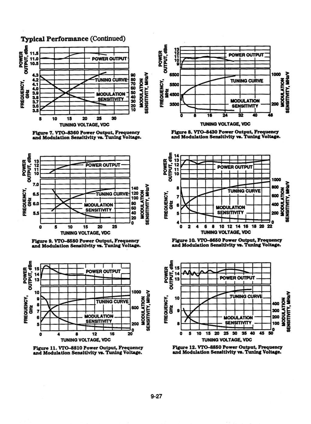
5 9-27
6 Typical Performance (Continued) POWER OUTPUT, dbm FREQUENCY, GHz POWER OUTPUT TUNING CURVE MODULATION SENSITIVITY MODULATION SENSITIVITY, MHz/V TUNING, VDC Figure 13. VTO 8950 Power Output, Frequency and Modulation Sensitivity vs. Tuning Voltage. LOG (f), dbc/hz k 10k 100k 1M FOURIER FREQUENCY, Hz 10M Figure 14. Noise Comparison Single Sideband Phase Noise. TO-8V Case Drawing DIA.45 DIA GLASS RING.060 DIA (3X).22 MIN V TUNE V + CASE APPROXIMATE WEIGHT 1.7 GRAMS NOTES (UNLESS OTHERWISE SPECIFIED): 1. DIMENSIONS ARE SPECIFIED IN INCHES 2. TOLERANCES: xx ±.02 xxx ±
7 Test Fixtures for TO-8 Packages (TF 801/802) Oscillators (VTO) Features DC to 11 GHz Frequency Range Connectorized Tuning Port and RF Output Easy to Test Package Repeatable Performance Applications Engineering Characterization Incoming Inspection System Prototype Demonstration of Device Performance Description To facilitate testing and prototyping of products in the TO-8V package, a series of test fixtures is available. Designated the HP TF Series test fixtures, they feature rugged construction for precise, repeatable measurements. The TF Series test fixtures come supplied with mounting hardware to ensure excellent ground contact between the oscillator package and test fixture. This assures excellent contact between package pins and test fixture connector pins for reliable testing. The device under test is aligned according to Figure 15, and pushed fully down onto the fixture. The steel mounting ring clamp is placed over the device under test and secured by machine screws prior to testing. Orientation of pins can be verified by comparison with part (c) of Figure 15. It is recommended that both machine screws be used to fasten the ring clamp. Screws should be tightened down snugly with a jewelers type screwdriver. For different connector options check the table in Figure 15 to identify the correct part numbers. It should be noted that some output power variation may be seen, from unit data, at frequencies above 8 GHz. This is due to small differences in lengths of test fixture RF output connector pins. VTO IN PLACE.53 TUNING CONNECTOR POWER INPUT CONNECTOR.35 + TUNING PIN TUNING DC PIN (a) (b) (c) V DC TAB ON PACKAGE SERIES TF-801 TF-802 CONNECTOR OPTIONS TUNING SMA SMA RF OUTPUT SMA E N + TUNING CASE.150 +DC (Bottom View) Figure 15. TO-8 Test Fixture. 9-29
Varactor-Tuned Oscillators. Technical Data. VTO-8000 Series. Pin Configuration TO-8V
 H Varactor-Tuned Oscillators Technical Data VTO-8 Series Features 6 MHz to.5 Coverage Fast Tuning +7 to + dbm Output Power ±1.5 db Output Flatness Hermetic Thin-film Construction Description HP VTO-8 Series
This provides extremely fast tuning speed limited primarily by the internal impedance of the user-supplied voltage driver.
 Hyperabrupt Varactor-Tuned Oscillators Technical Data VTO-9 Series Features 32 to 2.3 GHz Coverage Fast Tuning Fast Setting Time +2 VDC Max Tuning Voltage 1 mw Output Power ±2. db Output Flatness Hermetic
Features. = +25 C, Vdc = +12V
 Typical Applications The VCO Module is ideal for: Industrial/Medical Equipment Test & Measurement Equipment Military Radar, EW & ECM Lab Instrumentation Functional Diagram Electrical Specifications, T
INC. MICROWAVE. A Spectrum Control Business
 DRO Selection Guide DIELECTRIC RESONATOR OSCILLATORS Model Number Frequency Free Running, Mechanically Tuned Mechanical Tuning BW (MHz) +10 MDR2100 2.5-6.0 +10 6.0-21.0 +20 Free Running, Mechanically Tuned,
Features. = +25 C, Vcc = +5V
 Typical Applications Low noise wideband MMIC VCO for applications such as: Industrial/Medical Equipment Test & Measurement Equipment Military Radar, EW & ECM Functional Diagram Features Wide Tuning Bandwidth
Glossary of VCO terms
 Glossary of VCO terms VOLTAGE CONTROLLED OSCILLATOR (VCO): This is an oscillator designed so the output frequency can be changed by applying a voltage to its control port or tuning port. FREQUENCY TUNING
Features. = +25 C, Vcc = +3V
 Typical Applications Low noise MMIC VCO w/buffer Amplifi er for: Wireless Local Loop (WLL) VSAT & Microwave Radio Test Equipment & Industrial Controls Military Features Pout: +4.9 dbm Phase Noise: -3 dbc/hz
Features. = +25 C, Vcc = +3V
 Typical Applications Low noise MMIC VCO w/buffer Amplifi er for: VSAT & Microwave Radio Test Equipment & Industrial Controls Military Features Pout: +dbm Phase Noise: -106 dbc/hz @100 khz No External Resonator
Features. = +25 C, Vcc = +5V. Parameter Min. Typ. Max. Units Frequency Range GHz Power Output 3 dbm SSB Phase 10 khz Offset -60 dbc/hz
 Typical Applications Low Noise wideband MMIC VCO is ideal for: Industrial/Medical Equipment Test & Measurement Equipment Military Radar, EW & ECM Functional Diagram Features Wide Tuning Bandwidth Pout:
Analog Devices Welcomes Hittite Microwave Corporation NO CONTENT ON THE ATTACHED DOCUMENT HAS CHANGED
 Analog Devices Welcomes Hittite Microwave Corporation NO CONTENT ON THE ATTACHED DOCUMENT HAS CHANGED www.analog.com www.hittite.com THIS PAGE INTENTIONALLY LEFT BLANK Typical Applications Low noise wideband
Features. = +25 C, Vcc = +5V [1]
![Features. = +25 C, Vcc = +5V [1]](/thumbs/80/81652748.jpg "Features. = +25 C, Vcc = +5V [1]") Typical Applications Low Noise wideband MMIC VCO is ideal for: Features Wide Tuning Bandwidth Industrial/Medical Equipment Test & Measurement Equipment Military Radar, EW & ECM Functional Diagram Pout:
Typical Applications Low Noise wideband MMIC VCO is ideal for: Features Wide Tuning Bandwidth Industrial/Medical Equipment Test & Measurement Equipment Military Radar, EW & ECM Functional Diagram Pout:
12.92 GHz to GHz MMIC VCO with Half Frequency Output HMC1169
 Data Sheet 12.92 GHz to 14.07 GHz MMIC VCO with Half Frequency Output FEATURES Dual output frequency range fout = 12.92 GHz to 14.07 GHz fout/2 = 6.46 GHz to 7.035 GHz Output power (POUT): 11.5 dbm SSB
HMC358MS8G / 358MS8GE
 Typical Applications Low noise MMIC VCO w/buffer Amplifi er for C-Band applications such as: UNII & Pt. to Pt. Radios 802.a & HiperLAN WLAN VSAT Radios Features Pout: + dbm Phase Noise: -0 dbc/hz @100
Features. = +25 C, Vcc = +5V. Parameter Min. Typ. Max. Units Fo Fo/2 RFOUT RFOUT/2
 Typical Applications Low noise MMIC VCO w/half Frequency, for: VSAT Radio Point to Point/Multi-Point Radio Test Equipment & Industrial Controls Military End-Use Functional Diagram Features Dual Output:
12.17 GHz to GHz MMIC VCO with Half Frequency Output HMC1167
 9 0 3 4 5 6 9 7 6.7 GHz to 3.33 GHz MMIC VCO with Half Frequency Output FEATURES Dual output frequency range fout =.7 GHz to 3.330 GHz fout/ = 6.085 GHz to 6.665 GHz Output power (POUT): 0.5 dbm Single-sideband
11.41 GHz to GHz MMIC VCO with Half Frequency Output HMC1166
 9 6 3 30 29 VTUNE 28 27 26.4 GHz to 2.62 GHz MMIC VCO with Half Frequency Output FEATURES Dual output frequency range fout =.4 GHz to 2.62 GHz fout/2 = 5.705 GHz to 6.3 GHz Output power (POUT): dbm Single-sideband
Features. = +25 C, Vd1 = 3.6V, Vd2 = 20V, Vd3 = 6V
 Typical Applications The is ideal for: Military Radar, EW & ECM Test & Measurement Equipment Lab Instrumentation Industrial/Medical Equipment Functional Diagram Features Extremely Compact, Broadband Synthesizer
Features. = +25 C, Vcc = +5V. Parameter Min. Typ. Max. Units Fo Fo/2 RFOUT RFOUT/2
 v4.11 HMC5LP5 / 5LP5E OUTPUT 7.3 -.2 GHz Typical Applications Low noise MMIC VCO w/half Frequency, for: VSAT Radio Point to Point/Multi-Point Radio Test Equipment & Industrial Controls Military End-Use
EVALUATION KIT AVAILABLE 10MHz to 1050MHz Integrated RF Oscillator with Buffered Outputs. Typical Operating Circuit. 10nH 1000pF MAX2620 BIAS SUPPLY
 19-1248; Rev 1; 5/98 EVALUATION KIT AVAILABLE 10MHz to 1050MHz Integrated General Description The combines a low-noise oscillator with two output buffers in a low-cost, plastic surface-mount, ultra-small
PART MAX2605EUT-T MAX2606EUT-T MAX2607EUT-T MAX2608EUT-T MAX2609EUT-T TOP VIEW IND GND. Maxim Integrated Products 1
 19-1673; Rev 0a; 4/02 EVALUATION KIT MANUAL AVAILABLE 45MHz to 650MHz, Integrated IF General Description The are compact, high-performance intermediate-frequency (IF) voltage-controlled oscillators (VCOs)
9.25 GHz to GHz MMIC VCO with Half Frequency Output HMC1162
 9.5 GHz to 10.10 GHz MMIC VCO with Half Frequency Output HMC116 FEATURES FUTIONAL BLOCK DIAGRAM Dual output f OUT = 9.5 GHz to 10.10 GHz f OUT / = 4.65 GHz to 5.050 GHz Power output (P OUT ): 11 dbm (typical)
HMC6380LC4B. WIDEBAND VCOs - SMT. Electrical Specifications, T A. Typical Applications. Features. General Description. Functional Diagram
 Typical Applications Low Noise wideband MMIC VCO is ideal for: Industrial/Medical Equipment Test & Measurement Equipment Satcom Military Radar, EW, & ECM Functional Diagram Features Wide Tuning Bandwidth
Features. = +25 C, +Vdc = +6V, -Vdc = -5V
 v3.7 WIDEBAND LNA MODULE, - 2 GHz amplifiers Typical Applications The Wideband LNA is ideal for: Telecom Infrastructure Microwave Radio & VSAT Military & Space Test Instrumentation Industrial Sensors Functional
Features OBSOLETE. = +25 C, Vcc1, Vcc2 = +5.0V. Parameter Min. Typ. Max. Units Frequency Range GHz. Divided Output
 v3.81 Typical Applications Low noise MMIC VCO w/divide-by-8 for Ku-Band applications such as: Point-to-Point Radios Point-to-Multi-Point Radios / LMDS VSAT Functional Diagram Features Electrical Specifications,
Frequency vs. Tuning Voltage, Vcc = +4.2V 17 Frequency vs. Tuning Voltage, T= 25 C FREQUENCY (GHz) FREQUENCY (GHz) Vcc = 4.
 FREQUENCY (GHz) Vcc = 4.") Typical Applications The HMC736LP4(E) is ideal for: Point to Point/Multipoint Radio Test Equipment & Industrial Controls SATCOM Military End-Use Functional Diagram Features Dual Output: Fo = Fo/2 = 7.25-7.5
Typical Applications The HMC736LP4(E) is ideal for: Point to Point/Multipoint Radio Test Equipment & Industrial Controls SATCOM Military End-Use Functional Diagram Features Dual Output: Fo = Fo/2 = 7.25-7.5
Features. = +25 C, Vcc(RF), Vcc(DIG) = +5V
, Vcc(DIG) = +5V") & DIVIDE-BY-16, 23. - 26. GHz Typical Applications The HMC739LP4(E) is ideal for: Point-to-Point Radios Point-to-Multi-Point Radios / LMDS VSAT Features Pout: + dbm Phase Noise: -93 dbc/hz @ 100 khz Typ.
& DIVIDE-BY-16, 23. - 26. GHz Typical Applications The HMC739LP4(E) is ideal for: Point-to-Point Radios Point-to-Multi-Point Radios / LMDS VSAT Features Pout: + dbm Phase Noise: -93 dbc/hz @ 100 khz Typ.
Features. = +25 C, Vcc1, Vcc2 = +3V. Parameter Min. Typ. Max. Units Fo Fo/2 RFOUT RFOUT/2 RFOUT/4
 v4.11 Typical Applications Low noise MMIC VCO w/half Frequency, Divide-by-4 Outputs for: VSAT Radio Point to Point/Multipoint Radio Test Equipment & Industrial Controls Military End-Use Functional Diagram
Features. = +25 C, Vcc (Dig), Vcc (Amp), Vcc (RF) = +5V
, Vcc (Amp), Vcc (RF) = +5V") Typical Applications The HMC734LP5(E) is ideal for: Point-to-Point/Multi-Point Radio Test Equipment & Industrial Controls SATCOM Military End-Use Functional Diagram Features Dual Output: Fo = Fo/4 = 2.15-2.55
Typical Applications The HMC734LP5(E) is ideal for: Point-to-Point/Multi-Point Radio Test Equipment & Industrial Controls SATCOM Military End-Use Functional Diagram Features Dual Output: Fo = Fo/4 = 2.15-2.55
Features. = +25 C, Vcc1, Vcc2, Vcc3 = +5V. Parameter Min. Typ. Max. Units Frequency Range GHz
 Typical Applications Low noise MMIC VCO w/divide-by-16 for: VSAT Radio Point to Point/Multipoint Radio Test Equipment & Industrial Controls Military End-Use Automotive Radar Features Pout: + dbm Phase
Thin-Film Cascadable Amplifier 5 to 1000 MHz. Technical Data. UTO/UTC 1005 Series
 Thin-Film Cascadable Amplifier 5 to 1000 MHz Technical Data UTO/UTC 1005 Series Features Frequency Range: 5 to 1000 MHz High Dynamic Range High Output Power: +21.0 m (Typ) Noise Figure: 5.0 (Typ) Temperature
Features. = +25 C, Vcc1, Vcc2 = +5V. Parameter Min. Typ. Max. Units Fo Fo/2 RFOUT RFOUT/2 RFOUT/4
 v4.11 Typical Applications Low noise MMIC VCO w/half Frequency, Divide-by-4 Outputs for: VSAT Radio Point to Point/Multipoint Radio Test Equipment & Industrial Controls Military End-Use Functional Diagram
10MHz to 1050MHz Integrated RF Oscillator with Buffered Outputs
 9-24; Rev 2; 2/02 EVALUATION KIT AVAILABLE 0MHz to 050MHz Integrated General Description The combines a low-noise oscillator with two output buffers in a low-cost, plastic surface-mount, ultra-small µmax
Frequency vs. Tuning Voltage, Vcc = +5V OUTPUT FREQUENCY (GHz) Frequency vs. Tuning Voltage, T= 25 C OUTPUT F
 Frequency vs. Tuning Voltage, T= 25 C OUTPUT F") Typical Applications The HMC734LP5(E) is ideal for: Point-to-Point/Multi-Point Radio Test Equipment & Industrial Controls SATCOM Military End-Use Functional Diagram Features Dual Output: Fo = Fo/4 = 2.15-2.55
Typical Applications The HMC734LP5(E) is ideal for: Point-to-Point/Multi-Point Radio Test Equipment & Industrial Controls SATCOM Military End-Use Functional Diagram Features Dual Output: Fo = Fo/4 = 2.15-2.55
Features. = +25 C, Vcc (Dig), Vcc (Amp), Vcc (RF) = +5V. Parameter Min. Typ. Max. Units Fo Fo/4 RFOUT RFOUT/4
, Vcc (Amp), Vcc (RF) = +5V. Parameter Min. Typ. Max. Units Fo Fo/4 RFOUT RFOUT/4") .6-10.2 GHz Typical Applications The HMC734LP5(E) is ideal for: Point-to-Point/Multi-Point Radio Test Equipment & Industrial Controls SATCOM Military End-Use Functional Diagram Features Dual Output: Fo
.6-10.2 GHz Typical Applications The HMC734LP5(E) is ideal for: Point-to-Point/Multi-Point Radio Test Equipment & Industrial Controls SATCOM Military End-Use Functional Diagram Features Dual Output: Fo
Features. The HMC-C072 is ideal for: Microwave Radio Military & Space Test Instrumentation VSAT. = +25 C, Vdc = +7V
 amplifiers Typical Applications The is ideal for: Microwave Radio Military & Space Test Instrumentation VSAT Functional Diagram Features Ultra Low Phase Noise: -67 dbc/hz @ khz Noise Figure: 4.5 db Gain:
Features. Pout: +9 dbm. Parameter Min. Typ. Max. Units
 Typical Applications Phase-Locked Oscillator for: SAT Radio Point-to-Point & Point-to-Multi-Point Radio Test Equipment & Industrial Controls Military End-Use Functional Diagram Features Pout: +9 dbm Phase
Features. Packages. Applications
 8.4-9.1 GHz General Description The MMVC88 is designed in a highly reliable InGaP-GaAs Hetero-Junction Bipolar Transistor (HBT) process with active device, integrated resonator, tuning diode and isolating
MMIC VCO MMVC92. MMIC VCO GHz Type Q. General Description. Features. Packages. Functional Diagram. Applications
 8.6-9.5 GHz General Description The is designed in a highly reliable InGaP-GaAs Hetero-Junction Bipolar Transistor (HBT) process with active device, integrated resonator, tuning diode and isolating output
Features. = +25 C, Vcc (Dig), Vcc (Amp), Vcc (RF) = +5V. Parameter Min. Typ. Max. Units Fo Fo/2 RFOUT RFOUT/2 RFOUT/4
, Vcc (Amp), Vcc (RF) = +5V. Parameter Min. Typ. Max. Units Fo Fo/2 RFOUT RFOUT/2 RFOUT/4") HMC54LP5 / 54LP5E Typical Applications Low noise MMIC VCO w/half Frequency, Divide-by-4 Outputs for: Point to Point/Multipoint Radio Test Equipment & Industrial Controls SATCOM Military End-Use Functional
HMC54LP5 / 54LP5E Typical Applications Low noise MMIC VCO w/half Frequency, Divide-by-4 Outputs for: Point to Point/Multipoint Radio Test Equipment & Industrial Controls SATCOM Military End-Use Functional
Features. = +25 C, Vdc = +7V
 amplifiers Typical Applications The is ideal for: Microwave Radio Military & Space Test Instrumentation VSAT Functional Diagram Features Ultra Low Phase Noise: -7 dbc/hz @ khz Noise Figure: 6 db Gain:
Features. = +25 C, Vdc = +5V
 amplifiers Typical Applications The HMC-C is ideal for: Microwave Radio Military & Space Test Instrumentation VSAT Functional Diagram v.7 HMC-C Features Ultra Low Phase Noise: -6 dbc/hz @ khz Noise Figure:
Features. = +25 C, +Vdc = +6V, -Vdc = -5V
 HMC-C59 v.59 WIDEBAND LNA MODULE, - 2 GHz Typical Applications The HMC-C59 Wideband LNA is ideal for: Telecom Infrastructure Features Noise Figure:.8 db @ 8 GHz High Gain: 6 db @ 8 GHz PdB Output Power:
Features. Gain Variation Over Temperature db/ C
 HMC-C26 Features Typical Applications The HMC-C26 Wideband PA is ideal for: Telecom Infrastructure Microwave Radio & VSAT Military & Space Test Instrumentation Fiber Optics Functional Diagram Gain: 3 db
EDCRO-200 is a stable ceramic based, sampling phase locked oscillator.
 EDCRO-200 is a stable ceramic based, sampling phase locked oscillator. Commercial Military Airborne Space Missile Guidance Cable TV Links (CATV) Satellite Communications Low Cost External Reference Military/Commercial
Features. = +25 C, 50 Ohm System, Vcc = 5V. Parameter Conditions Min. Typ. Max. Units. Maximum Input Frequency GHz
 v2.1 DIVIDE-BY-, DC - 13 GHz Typical Applications Prescaler for DC to Ku Band PLL Applications: Point-to-Point / Multi-Point Radios VSAT Radios Fiber Optic Test Equipment Space & Military Functional Diagram
SC5407A/SC5408A 100 khz to 6 GHz RF Upconverter. Datasheet. Rev SignalCore, Inc.
 SC5407A/SC5408A 100 khz to 6 GHz RF Upconverter Datasheet Rev 1.2 2017 SignalCore, Inc. support@signalcore.com P R O D U C T S P E C I F I C A T I O N S Definition of Terms The following terms are used
MGA GHz 3 V, 17 dbm Amplifier. Data Sheet. Features. Description. Applications. Surface Mount Package. Simplified Schematic
 MGA-853.1 GHz 3 V, 17 dbm Amplifier Data Sheet Description Avago s MGA-853 is an economical, easy-to-use GaAs MMIC amplifier that offers excellent power and low noise figure for applications from.1 to
Product Guide. VIDA Oscillator Series. High Performance YIG Oscillator Westwind Blvd., Santa Rosa, CA Phone , FAX
 Product Guide VIDA Oscillator Series High Performance YIG Oscillator 3579 Westwind Blvd., Santa Rosa, CA 95403 Phone 707-541-7000, FAX 707-541-7030 REV 1 Sheet 1 of 8 However, no responsibility is assumed
RS3400W/04 77 GHz Radar Sensor
 Features Complete 76-77GHz band FMCW Radar Front End Synthesized frequency source Wideband Sweep Description The RS34W/4 is a W-band FMCW radar front end featuring synthesized frequency sweeps. A fast
Low Phase Noise C band HBT VCO. GaAs Monolithic Microwave IC
 Frequency (GHz) GaAs Monolithic Microwave IC Description The is a low phase noise C band HBT voltage controlled oscillator that integrates negative resistor, varactors and buffer amplifiers. It provides
24-bit Step Size, Resolution 3 Hz typ Exact Frequency Mode Built-in Digital Self Test 40 Lead 6x6mm SMT Package: 36mm 2. Phased Array Applications
 FRACTIONAL-N PLL WITH INTEGRATED VCO, 80-80 MHz Features RF Bandwidth: 80 to 80 MHz Ultra Low Phase Noise -110 dbc/hz in Band Typ. Figure of Merit (FOM) -22 dbc < 180 fs RMS Jitter 24-bit Step Size, Resolution
SDI SPECTRADYNAMICS, INC. LOW NOISE FREQUENCY REFERENCE OPERATING MANUAL
 SPECTRADYNAMICS, INC. LOW NOISE FREQUENCY REFERENCE LNFR-100E OPERATING MANUAL SPECTRADYNAMICS, INC 1849 Cherry St. Unit 2. Louisville, CO 80027 Phone: (303) 665-1852 Fax: (303) 604-6088 www.spectradynamics.com
RFVC1800 Wideband MMIC VCO with Buffer Amplifier 8GHz to 12GHz
 Wideband MMIC VCO with Buffer Amplifier 8GHz to 12GHz RFMD s wideband voltage controlled oscillator is a GaAs InGaP HBT MMIC with integrated VCO core and RF output buffer. The part operates from a single
Features. = +25 C, Vdd = 5V
 v3.117 HMC1LH5 Typical Applications The HMC1LH5 is a medium PA for: Telecom Infrastructure Military Radio, Radar & ECM Space Systems Test Instrumentation Functional Diagram Features Gain: 5 db Saturated
Phase Locked Sources Series PDRO Dielectric Resonator Oscillators
 Features Options Wide Operating Temperature Range -40 to +75 C Standard Ultra Low Phase-Noise Small Size Field Adjustable Tuning No Subharmonics Ideal for Outdoor Applications Low Cost, Low Profile, Low
Features. = +25 C, 50 Ohm System, Vcc= 5V
 Typical Applications Prescaler for 1 MHz to 13 GHz PLL Applications: Point-to-Point / Multi-Point Radios VSAT Radios Fiber Optic Test Equipment Space & Military Functional Diagram Features Ultra Low ssb
Military End-Use. Phased Array Applications. FMCW Radar Systems
 Features RF Bandwidth: 9.05 ghz to 10.15 ghz Fractional or Integer Modes Ultra Low Phase Noise 9.6 ghz; 50 MHz Ref. -106 / -102 dbc/hz @ 10 khz (Int / frac) dbc/hz @ 1 MHZ (Open Loop) Figure of Merit (FOM)
Application Note No. 099
 Application Note, Rev. 2.0, Feb. 0 Application Note No. 099 A discrete based 315 MHz Oscillator Solution for Remote Keyless Entry System using BFR182 RF Bipolar Transistor RF & Protection Devices Edition
OX-304 at 10 MHz Ultra Low Phase Noise Oven Controlled Crystal Oscillator
 OX-304 at 10 MHz Ultra Low Phase Noise Oven Controlled Crystal Oscillator OX-304 The OX-304 is an Ultra Low Phase Noise Ovenized Crystal Oscillator with a noise floor as low as -173 dbc/hz in a compact
Voltage-Controlled Oscillators Evaluated for System Design. Application Note M024
 Voltage-Controlled Oscillators Evaluated for System Design Application Note M024 High tuning speed, small size, and low power consumption make VCOs important components in a number of microwave applications.
Features. Gain: 17 db. OIP3: 25 dbm. = +25 C, Vdd 1, 2 = +3V
 v.7 HMCLC Typical Applications The HMCLC is ideal for use as a LNA or driver amplifier for: Point-to-Point Radios Point-to-Multi-Point Radios & VSAT Test Equipment and Sensors Military & Space Functional
LMX2604 Triple-band VCO for GSM900/DCS1800/PCS1900
 LMX2604 Triple-band VCO for GSM900/DCS1800/PCS1900 General Description The LMX2604 is a fully integrated VCO (Voltage-Controlled Oscillator) IC designed for GSM900/DCS1800/PCS1900 triple-band application.
1 MHz 6 GHz RF Mixer with built in PLL Synthesizer
 Windfreak Technologies Preliminary Data Sheet v0.1a MixNV Active Mixer v1.4a $499.00US 1 MHz 6 GHz RF Mixer with built in PLL Synthesizer Features Open source Labveiw GUI software control via USB Run hardware
GaAs MMIC devices are susceptible to Electrostatic Discharge. Use proper ESD precautions when handling these items.
 The is a broadband, power efficient GaAs PHEMT distributed amplifier in a 4mm QFN surface mount package. The is designed to provide optimal LO drive for T3 mixers. Typically, ADM-26-2931SM provides. db
Features. Parameter Min. Typ. Max. Units. Frequency Range 8 12 GHz Insertion Loss* db. Input Return Loss* 10 db
 v4.711 HMC-C Features Low RMS Phase Error: Low Insertion Loss: 7 db Excellent Flatness 3 Coverage, LSB = 22. Hermetically Sealed Module Field Replaceable SMA Female Connectors Typical Applications The
CUSTOM INTEGRATED ASSEMBLIES
 17 CUSTOM INTEGRATED ASSEMBLIES CUSTOM INTEGRATED ASSEMBLIES Cougar offers full first-level integration capabilities, providing not just performance components but also full subsystem solutions to help
VCO Design Project ECE218B Winter 2011
 VCO Design Project ECE218B Winter 2011 Report due 2/18/2011 VCO DESIGN GOALS. Design, build, and test a voltage-controlled oscillator (VCO). 1. Design VCO for highest center frequency (< 400 MHz). 2. At
Model 1152-ALN Phase Locked Oscillator
 Model 1152-ALN Phase Locked Oscillator The Model 1152-ALN is a single frequency, very low Phase Noise PLL unit that can be used to replace your unstable microwave crystal oscillator chain with a stable
MGA GHz 3 V, 17 dbm Amplifier. Data Sheet
 MGA-853.1 GHz 3 V, 17 dbm Amplifier Data Sheet Description Avago s MGA-853 is an economical, easy-to-use GaAs MMIC amplifier that offers excellent power and low noise figure for applications from.1 to
FREQUENCY AGILE FM MODULATOR INSTRUCTION BOOK IB
 FMT615C FREQUENCY AGILE FM MODULATOR INSTRUCTION BOOK IB1215-02 TABLE OF CONTENTS SECTION SUBJECT 1.0 Introduction 2.0 Installation & Operating Instructions 3.0 Specification 4.0 Functional Description
Low Noise Oscillator series LNO 4800 B MHz
 Specific request can be addressed to RAKON hirel@rakon.com Product Description LNO 4800 B3 is a low noise oscillator generating an output signal at 4800 MHz. It is composed by an OCSO (Oven Controlled
LBI-30398N. MAINTENANCE MANUAL MHz PHASE LOCK LOOP EXCITER 19D423249G1 & G2 DESCRIPTION TABLE OF CONTENTS. Page. DESCRIPTION...
 MAINTENANCE MANUAL 138-174 MHz PHASE LOCK LOOP EXCITER 19D423249G1 & G2 LBI-30398N TABLE OF CONTENTS DESCRIPTION...Front Cover CIRCUIT ANALYSIS... 1 MODIFICATION INSTRUCTIONS... 4 PARTS LIST AND PRODUCTION
Parameter Symbol Units MIN MAX. RF Input power (CW) Pin dbm +23
 Pin dbm +23") AMT-A0016 50MHz to 500MHz Limiting Amplifier Data Sheet Features Limiting Amplifier provides Pout> +12 dbm even with Pin varying from 18 dbm to 0 dbm Small Signal Gain 33 db Phase Noise 150 db @ 1KHz offset
AMT-A0016 50MHz to 500MHz Limiting Amplifier Data Sheet Features Limiting Amplifier provides Pout> +12 dbm even with Pin varying from 18 dbm to 0 dbm Small Signal Gain 33 db Phase Noise 150 db @ 1KHz offset
6 GHz to 26 GHz, GaAs MMIC Fundamental Mixer HMC773ALC3B
 FEATURES Conversion loss: 9 db typical Local oscillator (LO) to radio frequency (RF) isolation: 37 db typical LO to intermediate frequency (IF) isolation: 37 db typical RF to IF isolation: db typical Input
GaAs, MMIC Fundamental Mixer, 2.5 GHz to 7.0 GHz HMC557A
 FEATURES Conversion loss: db LO to RF isolation: db LO to IF isolation: 3 db Input third-order intercept (IP3): 1 dbm Input second-order intercept (IP2): dbm LO port return loss: dbm RF port return loss:
OBSOLETE HMC915LP4E. GaAs MMIC MIXER w/ INTEGRATED LO AMPLIFIER, GHz. Typical Applications. Features. Functional Diagram. General Description
 v1.5 LO AMPLIFIER,.5-2.7 GHz Typical Applications The is ideal for: PCS / 3G Infrastructure Base Stations & Repeaters WiMAX & WiBro ISM & Fixed Wireless Functional Diagram Features Input IP3: +28 dbm Low
= +25 C, Vcc = +3.3V, Z o = 50Ω (Continued)
") v1.1 HMC9LP3E Typical Applications The HMC9LP3E is ideal for: LO Generation with Low Noise Floor Software Defined Radios Clock Generators Fast Switching Synthesizers Military Applications Test Equipment
v1.1 HMC9LP3E Typical Applications The HMC9LP3E is ideal for: LO Generation with Low Noise Floor Software Defined Radios Clock Generators Fast Switching Synthesizers Military Applications Test Equipment
ERICSSONZ LBI-30398P. MAINTENANCE MANUAL MHz PHASE LOCKED LOOP EXCITER 19D423249G1 & G2 DESCRIPTION TABLE OF CONTENTS
 MAINTENANCE MANUAL 138-174 MHz PHASE LOCKED LOOP EXCITER 19D423249G1 & G2 TABLE OF CONTENTS Page DESCRIPTION... Front Cover CIRCUIT ANALYSIS...1 MODIFICATION INSTRUCTIONS...4 PARTS LIST...5 PRODUCTION
24-bit Step Size, Resolution 3 Hz typ Exact Frequency Mode Built-in Digital Self Test 40 Lead 6x6 mm SMT Package: 36 mm 2. Phased Array Applications
 Features Tri-band RF Bandwidth: Ultra Low Phase Noise -105 dbc/hz in Band Typ. Figure of Merit (FOM) -227 dbc/hz < 180 fs RMS Jitter 24-bit Step Size, Resolution 3 Hz typ Exact Frequency Mode Built-in
AN Demonstration of a 1GHz discrete VCO based on the BFR92A. Document information. Keywords Abstract
 Rev. 1.0 26 June 2012 Application note Document information Info Keywords Abstract Content Discrete, VCO, BFR92A, EVB, Design, Evaluation, Measurements This document provides an example of a discrete Voltage
24-bit Step Size, Resolution 3 Hz typ Exact Frequency Mode Built-in Digital Self Test 40 Lead 6x6mm SMT Package: 36mm 2. Phased Array Applications
 Features RF Bandwidth: 1815 to 2010 MHz Ultra Low Phase Noise -110 dbc/hz in Band Typ. Figure of Merit (FOM) -22 dbc < 180 fs RMS Jitter 24-bit Step Size, Resolution 3 Hz typ Exact Frequency Mode Built-in
SC5307A/SC5308A 100 khz to 6 GHz RF Downconverter. Datasheet SignalCore, Inc.
 SC5307A/SC5308A 100 khz to 6 GHz RF Downconverter Datasheet 2017 SignalCore, Inc. support@signalcore.com P RODUCT S PECIFICATIONS Definition of Terms The following terms are used throughout this datasheet
HIGH-VALUE PHASE-LOCKED COAXIAL RESONATOR OSCILLATOR
 OSCILLATOR SECTION HIGH-VALUE PHASE-LOCKED COAXIAL RESONATOR OSCILLATOR BCO SERIES: 0.20 4 GHz (Fundamental) 4 16 GHz (Multiplied) FEATURES Low cost Phase locked to external standard or internal crystal
GaAs MMIC devices are susceptible to Electrostatic Discharge. Use proper ESD precautions when handling these items.
 ADM-26-931SM The ADM-26-931SM is a broadband, power efficient GaAs PHEMT distributed amplifier in a 4mm QFN surface mount package. The ADM-26-931SM is designed to provide optimal LO drive for T3 mixers.
MAINTENANCE MANUAL FOR RECEIVER FRONT END MODULE 19D902782G5
 LBI-39028A IC DATA MAINTENANCE MANUAL FOR U1 19A704125P1 Quad Operational Amplifier U30 RYTUA901201/1 Power Module TABLE OF CONTENTS DESCRIPTION................................................ Front Cover
1 MHz to 2.7 GHz RF Gain Block AD8354
 1 MHz to 2.7 GHz RF Gain Block AD834 FEATURES Fixed gain of 2 db Operational frequency of 1 MHz to 2.7 GHz Linear output power up to 4 dbm Input/output internally matched to Ω Temperature and power supply
PXI MICROWAVE LOCAL OSCILLATOR MODULE
 The PXI-1450B Local Oscillator Module is a PXI 3U, 2-slot synthesizer module intended for frequency down conversion applications. The PXI-1450B is a VCO-based, 3 to 9 GHz synthesizer that uses QuickSyn
AT General Purpose, Low Current NPN Silicon Bipolar Transistor. Data Sheet
 AT-4532 General Purpose, Low Current NPN Silicon Bipolar Transistor Data Sheet Description Avago s AT-4532 is a general purpose NPN bipolar transistor that has been optimized for maximum f t at low voltage
CHV2411aQDG RoHS COMPLIANT
 RoHS COMPLIANT Fully Integrated HBT K-band VCO GaAs Monolithic Microwave IC in QFN package Description The CHV2411aQDG is a monolithic multifunction for frequency generation. It integrates an X-band push-push
Data Sheet. MGA GHz 3 V, 14 dbm Amplifier. Description. Features. Applications. Simplified Schematic
 MGA-8153.1 GHz 3 V, 1 dbm Amplifier Data Sheet Description Avago s MGA-8153 is an economical, easy-to-use GaAs MMIC amplifier that offers excellent power and low noise figure for applications from.1 to
Features OBSOLETE. = +25 C, IF= 1 GHz, USB, LO = +15 dbm [1]
![Features OBSOLETE. = +25 C, IF= 1 GHz, USB, LO = +15 dbm [1]](/thumbs/82/84974573.jpg "Features OBSOLETE. = +25 C, IF= 1 GHz, USB, LO = +15 dbm [1]") v1.414 HMC141LC4 Typical Applications The HMC141LC4 is Ideal for: Point-to-Point Radio Point-to-Multi-Point Radio Test Equipment & Sensors Military End Use Functional Diagram Features Wide IF Bandwidth:
v1.414 HMC141LC4 Typical Applications The HMC141LC4 is Ideal for: Point-to-Point Radio Point-to-Multi-Point Radio Test Equipment & Sensors Military End Use Functional Diagram Features Wide IF Bandwidth:
Features. = +25 C, VDD = +5 V, 0 dbm Drive Level [1]
![Features. = +25 C, VDD = +5 V, 0 dbm Drive Level [1]](/thumbs/85/92877431.jpg "Features. = +25 C, VDD = +5 V, 0 dbm Drive Level [1]") Typical Applications Features The HMC196LP3E is suitable for: Point-to-Point & VSAT Radios Test Instrumentation Military & Space Functional Diagram High Output Power: 12 dbm Low Input Power Drive: -2 to
Typical Applications Features The HMC196LP3E is suitable for: Point-to-Point & VSAT Radios Test Instrumentation Military & Space Functional Diagram High Output Power: 12 dbm Low Input Power Drive: -2 to
Features. = +25 C, Vcc = +5V, Z o = 50Ω, Bias1 = GND
 v1.612 Typical Applications The is ideal for: LO Generation with Low Noise Floor Clock Generators Mixer LO Drive Military Applications Test Equipment Sensors Functional Diagram Features Low Noise Floor:
LBI-38673C MAINTENANCE MANUAL FOR RECEIVER FRONT END MODULE 19D902782G3, G4, & G7 DESCRIPTION TABLE OF CONTENTS
 LBI-38673C MAINTENANCE MANUAL FOR 19D902782G3, G4, & G7 TABLE OF CONTENTS Page DESCRIPTION........................................... Front Cover SPECIFICATIONS.........................................
ericssonz LBI-38640E MAINTENANCE MANUAL FOR VHF TRANSMITTER SYNTHESIZER MODULE 19D902780G1 DESCRIPTION
 MAINTENANCE MANUAL FOR VHF TRANSMITTER SYNTHESIZER MODULE 19D902780G1 TABLE OF CONTENTS Page DESCRIPTION........................................... Front Cover GENERAL SPECIFICATIONS...................................
LBI-38673F MAINTENANCE MANUAL FOR RECEIVER FRONT END MODULE 19D902782G3, G4, & G7 DESCRIPTION TABLE OF CONTENTS
 MAINTENANCE MANUAL FOR 19D902782G3, G4, & G7 TABLE OF CONTENTS Page DESCRIPTION........................................... Front Cover SPECIFICATIONS......................................... 1 CIRCUIT
Technical Data IFD IFD-53110
 Silicon Bipolar MMIC 3.5 and 5.5 GHz Divide-by- Static Prescalers Technical Data IFD-53 IFD-53 Features Wide Operating Frequency Range: IFD-53:.5 to 5.5 GHz IFD-53:.5 to 3.5 GHz Low Phase Noise: -3 dbc/hz
77 GHz VCO for Car Radar Systems T625_VCO2_W Preliminary Data Sheet
 77 GHz VCO for Car Radar Systems Preliminary Data Sheet Operating Frequency: 76-77 GHz Tuning Range > 1 GHz Output matched to 50 Ω Application in Car Radar Systems ESD: Electrostatic discharge sensitive
AM Stabilized RF Amplifier Driver
 LIGO T00074 AM Stabilized RF Amplifier Driver SURF Project Final Report August 00 Jing Luo Mentor: Daniel Sigg Co Mentor: Paul Schwinberg Abstract: The AOM/EOM driver is a high power RF amplifier used