Advanced Design in Keysight. Genesys with Modelithics Models
|
|
|
- Marcia Molly Porter
- 5 years ago
- Views:
Transcription
1 Advanced Design in Keysight Genesys with Modelithics Models 1
2 What We ll Cover: What is the Modelithics COMPLETE Library? What are the key specialized features of Modelithics models for accurate simulation and quickly meeting design goals? Matching network optimization example in Keysight Genesys Latest updates and features of the Modelithics COMPLETE Library for Keysight Genesys 2
3 The Modelithics COMPLETE Library Modelithics models are measurement-based simulation models for RF and microwave electronic components, that feature many advanced features and capabilities The Modelithics library is a collection of these models: Over 520 models from over 50 popular vendors representing over 16,000* electronic components! The Modelithics COMPLETE Library includes: CLR Library NLT Library NLD Library SLC Library PLUS RLC component Microwave Global Models Non-linear transistor models Non-linear diode models System Level Component (filters, amplifiers, couplers, etc.) -Substrate Library -SPAR Library -Example Projects * Represents Modelithics COMPLETE Library for Keysight Genesys v17.2. Counts may vary by simulator. 3


4 Modelithics Microwave Global Models for Fast Design Optimization Part Value Scaling Solder Pad De-embedding Statistical Analysis Pad Scaling Horizontal/Vertical Orientation Substrate Scaling Part values can be optimized Substrate properties can be varied to evaluate effect on the design Statistical analysis can be used to predict yield and look into cost savings The models are compatible with EM co-simulation 4
5 Simple Matching Network Design Goals/Specs Use a lumped element design Input impedance series RLC: R=72Ω, C=10pF, L=0.405nH Output impedance: 50Ω Center frequency: 2.5GHz Substrate: 10 mil Rogers 4350B 5

6 Matching Network Synthesis in Keysight Genesys A quick way to start the synthesis is to select Impedance Match in the Getting Started window after launching Genesys. 6


7 Frequency Range *Center frequency = 2.5GHz Input = Series RLC Enter values for input impedance Match Network = LC Bandpass Order = 3 Output = 50Ω Enter Matching Network Properties 7
 3.902 C3 (pf) 3.419 C4 (pf) 0.683 S11=S22 C5 (pf) 1089.029 L2 (nh) 1.099 L3 (nh) 7.412 L4 (nh) 1.")
8 Ideal Matching Network Calculated Port_1 ZO=72 Ω Load C1 C=10 pf L1 L=0.405 nh C2 C=3.902 pf L2 L=1.099 nh L3 L=7.412 nh C3 C=3.419 pf C4 C=0.683 pf C5 C= pf L4 L=1.033 nh Port_2 ZO=50 Ω Element Value C2 (pf) C3 (pf) C4 (pf) S11=S22 C5 (pf) L2 (nh) L3 (nh) L4 (nh)

9 Next: Add Substrate and Replace Ideal Components with Modelithics Microwave Global Models 10 mil Rogers 4350B from Modelithics Substrate library Capacitor and inductor models from Modelithics CLR library Port_1 ZO=72 Ω IND_CLC_0302_001_1 CAP_PPI_0201N_001_2 IND_CLC_0302_001_3 Part=CoilCraft 0302CS Part="PassivePlus 0201N, ultra-low ESR" Part=CoilCraft 0302CS L=1.099 nh C=3.419 pf L=1.033 nh Sim_mode=0 - Full Parasitic Model Sim_mode=0 - Full Parasitic Model Sim_mode=0 - Full Parasitic Model Load C1 C=10 pf L1 L=0.405 nh CAP_PPI_0201N_001_1 Part="PassivePlus 0201N, ultra-low ESR" C=3.902 pf Sim_mode=0 - Full Parasitic Model IND_CLC_0302_001_2 Part=CoilCraft 0302CS L=7.412 nh Sim_mode=0 - Full Parasitic Model CAP_KMT_0603_001_1 Part=KEMET C0603 C= pf Sim_mode=0 - Full Parasitic Model CAP_PPI_0201N_001_3 Part="PassivePlus 0201N, ultra-low ESR" C=0.683 pf Sim_mode=0 - Full Parasitic Model Port_2 ZO=50 Ω *After adding parasitic models (using the ideal MN values), the matching network does not meet the design goals. 9
 3.902 4.923 C3 (pf) 3.419 4.171 C4 (pf) 0.683 0.523 C5 (pf) 1089.029 3332.719 L2 (nh) 1.099 1.")
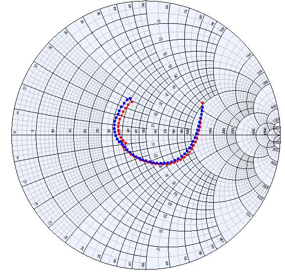
10 Re-optimize Matching Network Before (pink and green) and After (red and blue) optimization with parasitic models. Element Ideal Optimized with Modelithics models C2 (pf) C3 (pf) C4 (pf) C5 (pf) L2 (nh) L3 (nh) L4 (nh)

11 Add Microstrip Elements and Re-Optimize Microstrip elements are needed for evaluating any layout effects on the design. If any corrections are needed, it can be caught and updated in simulation before fabrication. Port_1 ZO=72 Ω IND_CLC_0302_001_1 Part=CoilCraft 0302CS L=1.505 nh Sim_mode=0 CAP_PPI_0201N_001_2 Part="PassivePlus 0201N, ultra-low ESR" C=4.171 pf Sim_mode=0 IND_CLC_0302_001_3 Part=CoilCraft 0302CS L=0.901 nh Sim_mode=0 Load C1 C=10 pf L1 L=0.405 nh TL1 CSTP1 CAP_PPI_0201N_001_1 CSTP2 W=21.7 mil [WLin] Part="PassivePlus 0201N, ultra-low ESR" C=4.923 pf Sim_mode=0 TL2 LSTP1 LSTP2 W=21.7 mil [WLin] 1 2 TL3 W=21.7 mil [WLin] TE1 TL4 W=21.7 mil [WLin] TL6 CSTP3 CSTP4 W=21.7 mil [WLin] 1 2 TL7 W=21.7 mil [WLin] TE2 TL8 W=21.7 mil [WLin] TL10 W=21.7 mil [WLin] CSTP7 CAP_KMT_0603_001_1 CSTP8 TL11 LSTP5 Part=KEMET C0603 W=21.7 mil [WLin] C= pf Sim_mode=0 LSTP6 Port_2 TL12 W=21.7 mil [WLin] ZO=50 Ω LSTP3 CSTP5 IND_CLC_0302_001_2 Part=CoilCraft 0302CS L=6.405 nh Sim_mode=0 CAP_PPI_0201N_001_3 Part="PassivePlus 0201N, ultra-low ESR" C=0.523 pf Sim_mode=0 LSTP4 CSTP6 TL5 W=24 mil L=12 mil TL15 W=24 mil L=12 mil VH1 VH2 CAD Layout TL13 W=24 mil L=12 mil TL14 W=24 mil L=12 mil Genesys Layout 11


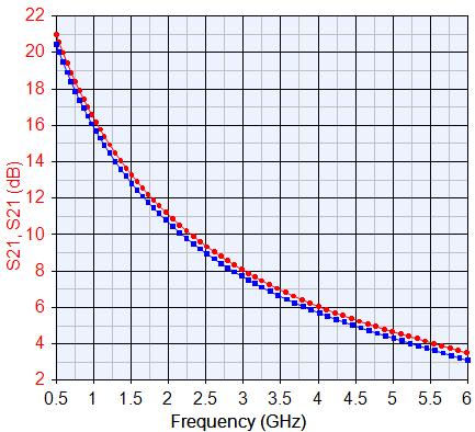
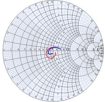
12 Before and After Optimization with Microstrip Elements Added Before Opt S11 S22 Ideal After Opt 12
 0.683 0.523 0.103 0.1 C5 (pf) 1089.029 3332.719 3299.643 3300 L2 (nh) 1.099 1.505 2.279 2.1 L3 (nh) 7.412 6.405 3.123 3 L4 (nh) 1.033 0.901 0.782 0.")
13 Choose Available Component Values* Element Ideal Optimized with Modelithics models Re-optimized with Microstrip Layout Available Values C2 (pf) C3 (pf) C4 (pf) C5 (pf) L2 (nh) L3 (nh) L4 (nh) Final design response *Discrete optimization is coming soon in the 2018 releases of Genesys and Modelithics, so this step will be automatic! 13
14 What s New in the Modelithics COMPLETE Library for Keysight Genesys? 48 new models in v17.2 for: ATC and AVX capacitors Chilisin ferrite beads Coilcraft inductors Johanson capacitors KEMET capacitors KOA resistors Murata capacitors and inductors Piconics conical inductors Presidio capacitor ST Micro capacitors Taiyo Yuden capacitors TDK capacitors and inductors Würth Elektronik inductors Skyworks Schottky diode Guerrilla RF LNA (SPAR/noise) Vanguard Electronics inductors and transformers (SPAR) Many new models coming in the next library release! (Planned Q3 2018) New features to be implemented in the upcoming Genesys SW release that take advantage of Modelithics model capabilities, including Vendor Part Synthesis and discrete optimization 14
15 Explore the capabilities of X-Parameters models 15
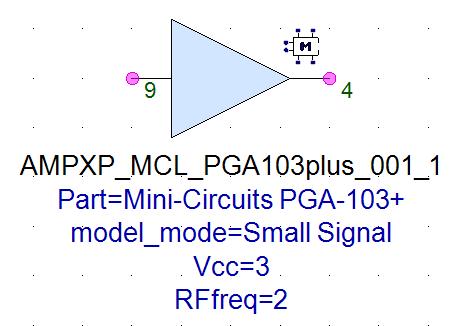
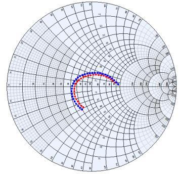
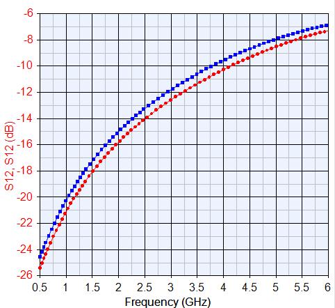
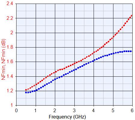
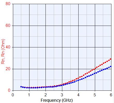
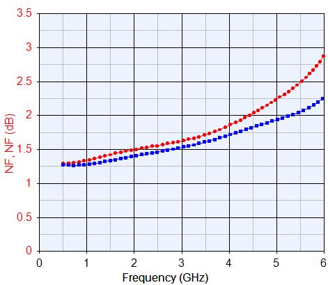
16 X-Parameters Models Small Signal Small signal S-Parameters and Noise Parameters performance SP and NP for Mini-Circuits PGA-103+ amplifier 5V 3V 16
17 X-Parameters Models Large Signal P1dB vs frequency and vendor data Red=Modeled Blue=Measured Black=Desired Output Power Red=Gain Blue=Compression Power and frequency sweep of an amplifier X- Parameter model Red=S11 at 21dBm Blue=S22 at 21dBm 17


18 Please let us know if you have any questions or if we may be of assistance. Web: Thank You!
Original Procedure by University of South Florida, Modified by Baylor University.
 1 ELC 4384 RF/Microwave Circuits II Spring 2018 Final Design Project: Design, Simulation, and Testing of a Low-Noise Amplifier Due Thursday, April 26, 12:30 p.m. Note: This procedure has been adapted from
Discrete Circuit Design
 Design Feature CHRIS DeMARTINO Technical Engineering Editor Take the Guesswork Out of Discrete Circuit Design A new software tool enables engineers to efficiently design circuits with models of actual
2005 Modelithics Inc.
 Precision Measurements and Models You Trust Modelithics, Inc. Solutions for RF Board and Module Designers Introduction Modelithics delivers products and services to serve one goal accelerating RF/microwave
surface mount chip ferrite bead model
 surface mount chip ferrite bead model Model Features Broadband (DC to 6GHz) Equivalent circuit based Substrate scalable (1. H/Er 16.4) Part value selectable: rated 1 to 18 ohms Bias Sensing Capability:
surface mount chip capacitor model
 surface mount chip capacitor model Model Features* Broadband validation: DC 30 GHz Equivalent circuit based Applicable for horizontal mounted capacitors Substrate scalable: (1 H/Er 16.7 mil) Part value
surface mount chip capacitor model
 S (db) CAP-PPI-78N- surface mount chip capacitor model Model Features* Broadband validation: DC 4 GHz Equivalent circuit based Substrate scalable:(.9 H/Er 6.5 mil) Part value scalable: (. to pf) Land Pattern
Using Accurate Component Models to Achieve First-Pass Success in Filter Design
 Application Example Using Accurate Component Models to Achieve First-Pass Success in Filter Design Overview Utilizing models that include component and printed circuit board (PCB) parasitics in place of
Maxim > Design Support > Technical Documents > Application Notes > Wireless and RF > APP 3571
 Maxim > Design Support > Technical Documents > Application Notes > Wireless and RF > APP 3571 Keywords: automotive keyless entry, MAX2640, LNA, 315MHz, RKE, stability, automotive, keyless entry APPLICATION
APPLICATION NOTE 052. A Design Flow for Rapid and Accurate Filter Prototyping
 APPLICATION NOTE 052 A Design Flow for Rapid and Accurate Filter Prototyping Introduction Filter designers for RF/microwave requirements are challenged with meeting an often-conflicting set of performance
Methodology for MMIC Layout Design
 17 Methodology for MMIC Layout Design Fatima Salete Correra 1 and Eduardo Amato Tolezani 2, 1 Laboratório de Microeletrônica da USP, Av. Prof. Luciano Gualberto, tr. 3, n.158, CEP 05508-970, São Paulo,
GHz Broadband Low Noise Amplifier
 .5 4. GHz Broadband Low Noise Amplifier Features Frequency Range:.5-4 GHz 1.8 db Mid-band Noise Figure 12.5 db Nominal Gain Very Low operating current (2V/15mA) Ideal Replacement for discrete devices 1dBm
Including the proper parasitics in a nonlinear
 Effects of Parasitics in Circuit Simulations Simulation accuracy can be improved by including parasitic inductances and capacitances By Robin Croston California Eastern Laboratories Including the proper
RF/Microwave Circuits I. Introduction Fall 2003
 Introduction Fall 03 Outline Trends for Microwave Designers The Role of Passive Circuits in RF/Microwave Design Examples of Some Passive Circuits Software Laboratory Assignments Grading Trends for Microwave
ECEN 4634/5634, MICROWAVE AND RF LABORATORY
 ECEN 4634/5634, MICROWAVE AND RF LABORATORY Final Exam December 18, 2017 7:30-10:00pm 150 minutes, closed book, 1 sheet allowed, no calculators (estimates need to be within 3dB) Part 1 (60%). Briefly answer
ELC 4396 RF/Microwave Circuits I Fall 2011 Final Exam December 9, 2011 Open Book/Open Notes 2 hours
 Name ELC 4396 RF/Microwave Circuits I Fall 2011 Final Exam December 9, 2011 Open Book/Open Notes 2 hours 1. The exam is open-book/open-notes. 2. A calculator may be used to assist with the test. No laptops
EXEMPLAR LIBRARY LIBRARY USER MANUAL (V11) For Agilent Technologies Advanced Design System
 For Agilent Technologies Advanced Design System") MODELITHICS EXEMPLAR LIBRARY LIBRARY USER MANUAL (V11) For Agilent Technologies Advanced Design System CONTENTS CONTENTS... 2 INSTALLATION INSTRUCTIONS... 8 OVERVIEW... 11 CLR LIBRARY... 11 NLD LIBRARY...
MODELITHICS EXEMPLAR LIBRARY LIBRARY USER MANUAL (V11) For Agilent Technologies Advanced Design System CONTENTS CONTENTS... 2 INSTALLATION INSTRUCTIONS... 8 OVERVIEW... 11 CLR LIBRARY... 11 NLD LIBRARY...
SKY LF: Low Noise Amplifier Operation
 application note SKY655-372LF: Low Noise Amplifier Operation Introduction The SKY655-372LF is a high performance, low noise, n-channel, depletion mode phemt, fabricated from Skyworks advanced phemt process
Application Note 5525
 Using the Wafer Scale Packaged Detector in 2 to 6 GHz Applications Application Note 5525 Introduction The is a broadband directional coupler with integrated temperature compensated detector designed for
Wide-Band Two-Stage GaAs LNA for Radio Astronomy
 Progress In Electromagnetics Research C, Vol. 56, 119 124, 215 Wide-Band Two-Stage GaAs LNA for Radio Astronomy Jim Kulyk 1,GeWu 2, Leonid Belostotski 2, *, and James W. Haslett 2 Abstract This paper presents
Gallium Nitride MMIC 5W DC 10.0 GHz Power Amplifier
 Gallium Nitride MMIC W DC. GHz Power Amplifier Oct 17 P2 DESCRIPTION AMCOM s is a broadband GaN MMIC power amplifier. It has 13dB gain, and 37 dbm output power over the DC to GHz band. The is in a ceramic
ABA GHz Broadband Silicon RFIC Amplifier. Application Note 1349
 ABA-52563 3.5 GHz Broadband Silicon RFIC Amplifier Application Note 1349 Introduction Avago Technologies ABA-52563 is a low current silicon gain block RFIC amplifier housed in a 6-lead SC 70 (SOT- 363)
Application Note 1360
 ADA-4743 +17 dbm P1dB Avago Darlington Amplifier Application Note 1360 Description Avago Technologies Darlington Amplifier, ADA-4743 is a low current silicon gain block RFIC amplifier housed in a 4-lead
Application Note 5057
 A 1 MHz to MHz Low Noise Feedback Amplifier using ATF-4143 Application Note 7 Introduction In the last few years the leading technology in the area of low noise amplifier design has been gallium arsenide
Accurate Simulation of RF Designs Requires Consistent Modeling Techniques
 From September 2002 High Frequency Electronics Copyright 2002, Summit Technical Media, LLC Accurate Simulation of RF Designs Requires Consistent Modeling Techniques By V. Cojocaru, TDK Electronics Ireland
MMA D 30KHz-50GHz Traveling Wave Amplifier With Output Power Detector Preliminary Data Sheet
 Features: Frequency Range: 30KHz 50 GHz P1dB: +22 dbm Vout: 7V p-p @50Ω Gain: 15.5 db Vdd =7 V Ids = 200 ma Input and Output Fully Matched to 50 Ω On-Chip Output Power Voltage Detector Die Size 2.35mm
Anaren 0805 (B0809J50ATI) balun optimized for Texas Instruments CC1100/CC1101 Transceiver
 balun optimized for Texas Instruments CC1100/CC1101 Transceiver") (ANN-2005) Rev B Page 1 of 13 Anaren 0805 (B0809J50ATI) balun optimized for Texas Instruments CC1100/CC1101 Transceiver Trong N Duong RF Co-Op Nithya R Subramanian RF Engineer Introduction The tradeoff
(ANN-2005) Rev B Page 1 of 13 Anaren 0805 (B0809J50ATI) balun optimized for Texas Instruments CC1100/CC1101 Transceiver Trong N Duong RF Co-Op Nithya R Subramanian RF Engineer Introduction The tradeoff
High IP3 Low-Noise Amplifier
 EVALUATION KIT AVAILABLE General Description The low-cost, high third-order intercept point (IP3) low-noise amplifier (LNA) is designed for applications in 2.4GHz WLAN, ISM, and Bluetooth radio systems.
Substrate Libraries Ease PCB Simulations
 1 of 6 3/25/2013 10:38 PM print close Substrate Libraries Ease PCB Simulations Scott Muir, Eric O'Dell, Laura Levesque, Hugo Morales, and Larry Dunleavy Tue, 2013-02-26 14:13 These measurement-based substrate
Maxim Integrated Products 1
 9-92; Rev 0; /0 MAX2242 Evaluation Kit General Description The MAX2242 evaluation kit (EV kit) simplifies evaluation of the MAX2242 power amplifier (PA), which is designed for 2.4GHz ISM-band direct-sequence
RoHS Compliant MAAPSS0103 V3. High Power Linear Amplifier GHz. Pin Configuration. Features. Block Diagram. Description. Ordering Information 1
 Features Ideal for WiMax, MESH Network, and Linear Applications P1dB: +32 dbm Typical Small Signal Gain: 34 db Typical EVM: 2.5% at 26 dbm Linear (OFDM) P OUT Integrated Detector Lead-Free 4 mm 16 lead
INVENTION DISCLOSURE- ELECTRONICS SUBJECT MATTER IMPEDANCE MATCHING ANTENNA-INTEGRATED HIGH-EFFICIENCY ENERGY HARVESTING CIRCUIT
 INVENTION DISCLOSURE- ELECTRONICS SUBJECT MATTER IMPEDANCE MATCHING ANTENNA-INTEGRATED HIGH-EFFICIENCY ENERGY HARVESTING CIRCUIT ABSTRACT: This paper describes the design of a high-efficiency energy harvesting
Leveraging High-Accuracy Models to Achieve First Pass Success in Power Amplifier Design
 Application Note Leveraging High-Accuracy Models to Achieve First Pass Success in Power Amplifier Design Overview Nonlinear transistor models enable designers to concurrently optimize gain, power, efficiency,
400 MHz to 4000 MHz ½ Watt RF Driver Amplifier ADL5324
 Data Sheet FEATURES Operation from MHz to MHz Gain of 14.6 db at 21 MHz OIP of 4.1 dbm at 21 MHz P1dB of 29.1 dbm at 21 MHz Noise figure of.8 db Dynamically adjustable bias Adjustable power supply bias:.
800 to 950 MHz Amplifiers using the HBFP-0405 and HBFP-0420 Low Noise Silicon Bipolar Transistors. Application Note 1161
 8 to 95 MHz Amplifiers using the HBFP-45 and HBFP-42 Low Noise Silicon Bipolar Transistors Application Note 1161 Introduction Hewlett-Packard s HBFP-45 and HBFP-42 are high performance isolated collector
SKY LF: GHz Low Noise Amplifier
 DATA SHEET SKY6538-7LF:.25-6. GHz Low Noise Amplifier Applications Wireless infrastructure: WLAN, WiMAX, broadband, cellular base stations Test instrumentation Cable television Features Broadband frequency
Design and Optimization of Lumped Element Hybrid Couplers
 From August 2011 Copyright 2011, Summit Technical Media, LLC Design and Optimization of Lumped Element Hybrid Couplers By Ashok Srinivas Vijayaraghavan, University of South Florida and Lawrence Dunleavy,
MMA C 30KHz-50GHz Traveling Wave Amplifier Data Sheet
 Features: Frequency Range: 30KHz 50 GHz P1dB: +22 dbm Vout: 7V p-p @50Ω Gain: 15.5 db Vdd =7 V Ids = 200 ma Input and Output Fully Matched to 50 Ω on chip Applications: Fiber optics communication systems
Application Note 5012
 MGA-61563 High Performance GaAs MMIC Amplifier Application Note 5012 Application Information The MGA-61563 is a high performance GaAs MMIC amplifier fabricated with Avago Technologies E-pHEMT process and
DESCRIPTIO FEATURES APPLICATIO S. LT GHz to 2.7GHz Receiver Front End TYPICAL APPLICATIO
 1.GHz to 2.GHz Receiver Front End FEATURES 1.V to 5.25V Supply Dual LNA Gain Setting: +13.5dB/ db at Double-Balanced Mixer Internal LO Buffer LNA Input Internally Matched Low Supply Current: 23mA Low Shutdown
LTE Small-Cell Base Station Antenna Matched for Maximum Efficiency
 Application Note LTE Small-Cell Base Station Antenna Matched for Maximum Efficiency Overview When designing antennas for base stations and mobile devices, an essential step of the design process is to
Genesys 2012 Tutorial 2 - Using Momentum Analysis for Microwave Planar Circuits: Circuit and EM Co-Simulation
 Genesys 2012 Tutorial 2 - Using Momentum Analysis for Microwave Planar Circuits: Circuit and EM Co-Simulation Here we demonstrate the process of running circuit and EM (electromagnetic) co-simulation.
RF Power LDMOS Transistors High Ruggedness N--Channel Enhancement--Mode Lateral MOSFETs
 Technical Data RF Power LDMOS Transistors High Ruggedness N--Channel Enhancement--Mode Lateral MOSFETs These high ruggedness devices are designed for use in high VSWR industrial, scientific and medical
Case Study: Osc2 Design of a C-Band VCO
 MICROWAVE AND RF DESIGN Case Study: Osc2 Design of a C-Band VCO Presented by Michael Steer Reading: Chapter 20, 20.5,6 Index: CS_Osc2 Based on material in Microwave and RF Design: A Systems Approach, 2
100 Genesys Design Examples
 [Type here] [Type here] [Type here] 100 Genesys Design Examples A Design Approach using (Genesys): Chapter 2: Transmission Line Components Ali Behagi 100 Genesys Design Examples A Design Approach using
Enhancement Mode phemt
 Freescale Semiconductor Technical Data Enhancement Mode phemt Technology (E -phemt) Low Noise Amplifier The MML25231H is a single--stage low noise amplifier (LNA) with active bias and high isolation for
800MHz BAND LOW NOISE AMPLIFIER GaAs MMIC
 NJG14KB 8MHz BAND LOW NOISE AMPLIFIER GaAs MMIC GENERAL DESCRIPTION PACKAGE OUTLINE NJG14KB is a variable gain low noise amplifier (LNA). At 8MHz band, noise figure is 1.dB, variable gain re is 1dB and
RF Circuit Synthesis for Physical Wireless Design
 RF Circuit Synthesis for Physical Wireless Design Overview Subjects Review Of Common Design Tasks Break Down And Dissect Design Task Review Non-Synthesis Methods Show A Better Way To Solve Complex Design
CMY210. Demonstration Board Documentation / Applications Note (V1.0) Ultra linear General purpose up/down mixer 1. DESCRIPTION
 Ultra linear General purpose up/down mixer 1. DESCRIPTION") Demonstration Board Documentation / (V1.0) Ultra linear General purpose up/down mixer Features: Very High Input IP3 of 24 dbm typical Very Low LO Power demand of 0 dbm typical; Wide input range Wide LO
Demonstration Board Documentation / (V1.0) Ultra linear General purpose up/down mixer Features: Very High Input IP3 of 24 dbm typical Very Low LO Power demand of 0 dbm typical; Wide input range Wide LO
Application Note A008
 Microwave Oscillator Design Application Note A008 Introduction This application note describes a method of designing oscillators using small signal S-parameters. The background theory is first developed
LT GHz to 3.8GHz High Linearity Upconverting Mixer. Description. Features. Applications. Typical Application
 Features n High Output IP3: +7.3 at.1ghz n Low Noise Floor: /Hz (P OUT = 5) n High Conversion Gain:. at.1ghz n Wide Frequency Range: 1.5GHz to 3.GHz* n Low LO Leakage n Single-Ended RF and LO n Low LO
MAX2683/MAX2684 Evaluation Kits
 9-6; Rev ; / MAX68/MAX684 Evaluation Kits General Description The MAX68/MAX684 evaluation kits (EV kits) simplify evaluation of the MAX68/MAX684.4GHz to.8ghz downconverter mixers. The EV kits are fully
3.8 GHz Linear Power Amplifier and BTS Driver High Efficiency/Linearity Amplifier
 Technical Data 3.8 GHz Linear Power Amplifier and BTS Driver High Efficiency/Linearity Amplifier The MMZ38333B is a 3--stage high linearity InGaP HBT broadband amplifier designed for small cells and LTE
ATF-501P8. Application Note MHz High Linearity Amplifier
 ATF-501P8 450 MHz High Linearity Amplifier Application Note 5058 ATF-501P8 Applications Information Description Avago Technologies ATF-501P8 is an enhancement mode PHEMT designed for high linearity and
Application Note 1285
 Low Noise Amplifiers for 5.125-5.325 GHz and 5.725-5.825 GHz Using the ATF-55143 Low Noise PHEMT Application Note 1285 Description This application note describes two low noise amplifiers for use in the
825MHz to 915MHz, SiGe High-Linearity Active Mixer
 19-2489; Rev 1; 9/02 825MHz to 915MHz, SiGe High-Linearity General Description The fully integrated SiGe mixer is optimized to meet the demanding requirements of GSM850, GSM900, and CDMA850 base-station
Application Note 1131
 Low Noise Amplifiers for 320 MHz and 850 MHz Using the AT-32063 Dual Transistor Application Note 1131 Introduction This application note discusses the Avago Technologies AT-32063 dual low noise silicon
Application Note 5038
 MGA-6P8 Buffer Amplifier for 10 MHz Application Application Note 038 Introduction The MGA-6P8 is a high isolation buffer amplifier based on Avago Technologies EPHEMT process. This application note discusses
Non-Linear Transmission Line Comb Generator
 Page 1 The is a GaAs Schottky diode based non-linear transmission line comb generator. It is optimized for at input frequencies of 1 16 GHz and minimum input drive powers of +16 dbm. Harmonic content is
Application Note 5460
 MGA-89 High Linearity Amplifier with Low Operating Current for 9 MHz to. GHz Applications Application Note 6 Introduction The Avago MGA-89 is a high dynamic range amplifier designed for applications in
Microwave Oscillator Design. Application Note A008
 Microwave Oscillator Design Application Note A008 NOTE: This publication is a reprint of a previously published Application Note and is for technical reference only. For more current information, see the
0.5-4GHz Low Noise Amplifier
 .5-4GHz Low Noise Amplifier Features Frequency Range:.5-4 GHz Better than 2.dB Noise Figure Single supply operation db Nominal Gain dbm Nominal P1dB Input Return Loss > db Output Return Loss > db DC decoupled
This article describes the design of a multiband,
 A Low-Noise Amplifier for 2 GHz Applications Using the NE334S01 Transistor By Ulrich Delpy NEC Electronics (Europe) This article describes the design of a multiband, low-noise amplifier (LNA) using the
0.5-4GHz Low Noise Amplifier
 ASL P3.5-4GHz Low Noise Amplifier Features Frequency Range:.5-4 GHz Better than 2.dB Noise Figure Single supply operation db Nominal Gain dbm Nominal P1dB Input Return Loss > db Output Return Loss > db
Monolithic Amplifier TSY-13LNB+ Wideband. 50Ω 0.03 to 1 GHz. The Big Deal
 Wideband Monolithic Amplifier 50Ω 0.03 to 1 GHz The Big Deal Very wideband, 30 MHz 1 GHz Low NF over entire frequency band, 1.2 db Low current and low voltage (2.7V and 7.7 ma) Internal bypass switching
2 W High Gain Power Amplifier for Cellular Infrastructure InGaP GaAs HBT
 Technical Data 2 W High Gain Power Amplifier for Cellular Infrastructure InGaP GaAs HBT The MMZ27333B is a versatile 3--stage power amplifier targeted at driver and pre--driver applications for macro and
Application Note 5011
 MGA-62563 High Performance GaAs MMIC Amplifier Application Note 511 Application Information The MGA-62563 is a high performance GaAs MMIC amplifier fabricated with Avago Technologies E-pHEMT process and
300 frequencies is calculated from electromagnetic analysis at only four frequencies. This entire analysis takes only four minutes.
 Electromagnetic Analysis Speeds RFID Design By Dr. James C. Rautio Sonnet Software, Inc. Liverpool, NY 13088 (315) 453-3096 info@sonnetusa.com http://www.sonnetusa.com Published in Microwaves & RF, February
GaAs MMIC devices are susceptible to Electrostatic Discharge. Use proper ESD precautions when handling these items.
 ADM-12-931SM The ADM-12-931SM is a small, low power, and economical T3 driver or T3A pre-amplifier. It is a GaAs PHEMT distributed amplifier in a 3mm QFN surface mount package. The ADM-12-931SM can provide
A GSM Band Low-Power LNA 1. LNA Schematic
 A GSM Band Low-Power LNA 1. LNA Schematic Fig1.1 Schematic of the Designed LNA 2. Design Summary Specification Required Simulation Results Peak S21 (Gain) > 10dB >11 db 3dB Bandwidth > 200MHz (
433MHz Single Chip RF Transmitter
 433MHz Single Chip RF Transmitter nrf402 FEATURES True single chip FSK transmitter Few external components required On chip UHF synthesiser No set up or configuration 20kbit/s data rate 2 channels Very
RF Power LDMOS Transistors High Ruggedness N--Channel Enhancement--Mode Lateral MOSFETs
 Technical Data Document Number: MRF101AN Rev. 0, 11/18 RF Power LDMOS Transistors High Ruggedness N--Channel Enhancement--Mode Lateral MOSFETs These devices are designed for use in VHF/UHF communications,
SKY LF: GHz High Linearity, Active Bias Low-Noise Amplifier
 PRELIMINARY DATA SHEET SKY671-396LF: 1.7-2. GHz High Linearity, Active Bias Low-Noise Amplifier Applications GSM, CDMA, WCDMA, and TD-SCDMA cellular infrastructure Ultra low-noise systems Features Ultra
2 W High Gain Power Amplifier for Cellular Infrastructure InGaP GaAs HBT
 Freescale Semiconductor Technical Data 2 W High Gain Power Amplifier for Cellular Infrastructure InGaP GaAs HBT The MMZ25333B is a versatile 3--stage power amplifier targeted at driver and pre--driver
Low Noise Amplifier for 3.5 GHz using the Avago ATF Low Noise PHEMT. Application Note 1271
 Low Noise Amplifier for 3. GHz using the Avago ATF-3143 Low Noise PHEMT Application Note 171 Introduction This application note describes a low noise amplifier for use in the 3.4 GHz to 3.8 GHz wireless
MSW2T /MSW2T SP2T Surface Mount High Power PIN Diode Switch
 RELEASED MSW2T-2040-193/MSW2T-2041-193 SP2T Surface Mount High Power PIN Diode Switch Features: Wide Operating Frequency Band: 50 MHz to 4 GHz Surface Mount SP2T Switch: 5mm x 8mm x 2.5mm Industry Leading
Data Sheet. MGA-632P8 Low Noise, High Linearity Active Bias Low Noise Amplifier. Features. Description. Specifications.
 MGA-632P8 Low Noise, High Linearity Active Bias Low Noise Amplifier Data Sheet Description Avago Technologies MGA-632P8 is an economical, easyto-use GaAs MMIC Low Noise Amplifier (LNA) with active bias.
Application Note No. 181
 Application Note, Rev. 2.1, July 2010 Application Note No. 181 FM Radio LNA using BGB707L7ESD matched to 50 Ω, including application proposal for ESD protection RF & Protection Devices Edition 2010-07-07
ATE Loadboard Layout for High Density RF Applications. Presented by: Heidi Barnes. In collaboration with: Oscar Solano Martin Dresler Vanessa Bischler
 ATE Loadboard Layout for High Density RF Applications Presented by: Heidi Barnes In collaboration with: Oscar Solano Martin Dresler Vanessa Bischler Abstract ❿ The current success of smart-phones and the
SKY LF: GHz Low Noise Amplifier
 DATA SHEET SKY6548-36LF:.7-1.2 GHz Low Noise Amplifier Applications Wireless infrastructure: GSM, CDMA, WCDMA, ISM, and TD-SCDMA Ultra-low noise applications Features Ultra-low Noise Figure =.65 db @ 9
SKY LF: GHz High Linearity, Active Bias Low-Noise Amplifier
 DATA SHEET SKY67102-396LF: 2.0-3.0 GHz High Linearity, Active Bias Low-Noise Amplifier Applications CDMA, WCDMA, TD-SCDMA, WiMAX, and LTE cellular infrastructure Ultra low-noise systems Features Ultra
Measured RF Performance Summary
 Summary Application Note The AP603 is a high dynamic range power amplifier in a lead-free/rohs-compliant 5x6mm power DFN SMT package. It features an internal active-bias circuit that provides temperature
BROADBAND DISTRIBUTED AMPLIFIER
 ADM-126-83SM The ADM-126-83SM is a broadband, efficient GaAs PHEMT distributed amplifier with an integrated bias tee in a 4mm QFN surface mount package, designed to provide efficient LO drive for T3 mixers.
Driver or Pre -driver Amplifier for Doherty Power Amplifiers
 Technical Data Driver or Pre -driver Amplifier for Doherty Power Amplifiers The MMG30301B is a 1 W high gain amplifier designed as a driver or pre--driver for Doherty power amplifiers in wireless infrastructure
SKY LF: 0.4 to 1.2 GHz High Linearity, Active Bias Low-Noise Amplifier
 DATA SHEET SKY6711-396LF:.4 to 1.2 GHz High Linearity, Active Bias Low-Noise Amplifier Applications GSM, CDMA, WCDMA, and TD-SCDMA cellular infrastructure Ultra low-noise systems Features Ultra-low-noise
Application Note 5499
 MGA-31389 and MGA-31489 High-Gain Driver Amplifier Using Avago MGA-31389 and MGA-31489 Application Note 5499 Introduction The MGA-31389 and MGA-31489 from Avago Technologies are.1 Watt flat-gain driver
The L Chip Technology Comparison A Technical-Competitive Analysis of Ceramic Chip Inductor Manufacturers
 The L Chip Technology Comparison A Technical-Competitive Analysis of Ceramic Chip Inductor Manufacturers Published November 2017 Price: $1800.00 USD Pages: 103 Tables & Graphs: 49 ISBN #:1-893211-99-1
Monolithic Amplifier EHA-163L+ Low Current, Wideband, Flat Gain. 50Ω DC to 16 GHz. The Big Deal
 Low Current, Wideband, Flat Gain Monolithic Amplifier 50Ω DC to 16 GHz The Big Deal Super Wideband, DC to 16 GHz Excelent Gain Flatness, ±0.75 up to 12 GHz Low Current, 20 ma CASE STYLE: MC1630-1 Product
International Journal of Science and Engineering Investigations vol. 2, issue 15, April 2013
 International Journal of Science and Engineering Investigations vol. 2, issue 15, April 2013 ISSN: 2251-8843 A New Analytical Approach for Developing an Equivalent Circuit Simulation Model for a Chip Inductor,
Microwave and RF Engineering
 Microwave and RF Engineering A Simulation Approach with Keysight Genesys Software Chapter 4: Resonant Circuits and Filters Ali A. Behagi Stephen D. Turner Microwave and RF Engineering A Simulation Approach
Surface Mount SOT-363 (SC-70) Package. Pin Connections and Package Marking GND. V dd. Note: Package marking provides orientation and identification.
 Package. Pin Connections and Package Marking GND. V dd. Note: Package marking provides orientation and identification.") GHz V Low Current GaAs MMIC LNA Technical Data MGA-876 Features Ultra-Miniature Package.6 db Min. Noise Figure at. GHz. db Gain at. GHz Single + V or V Supply,. ma Current Applications LNA or Gain Stage
GHz V Low Current GaAs MMIC LNA Technical Data MGA-876 Features Ultra-Miniature Package.6 db Min. Noise Figure at. GHz. db Gain at. GHz Single + V or V Supply,. ma Current Applications LNA or Gain Stage
MSW2T /MSW2T /MSW2T SP2T Surface Mount High Power PIN Diode Switch
 PRELIMINARY MSW2T-2030-192/MSW2T-2031-192/MSW2T-2032-192 SP2T Surface Mount High Power PIN Diode Switch Features: Wide Operating Frequency Band: 50 MHz to 6 GHz Surface Mount SP2T Switch 5mm x 8mm x 2.5mm
EVALUATION KIT AVAILABLE 10MHz to 1050MHz Integrated RF Oscillator with Buffered Outputs. Typical Operating Circuit. 10nH 1000pF MAX2620 BIAS SUPPLY
 19-1248; Rev 1; 5/98 EVALUATION KIT AVAILABLE 10MHz to 1050MHz Integrated General Description The combines a low-noise oscillator with two output buffers in a low-cost, plastic surface-mount, ultra-small
Design and Demonstration of a Passive, Broadband Equalizer for an SLED Chris Brinton, Matthew Wharton, and Allen Katz
 Introduction Design and Demonstration of a Passive, Broadband Equalizer for an SLED Chris Brinton, Matthew Wharton, and Allen Katz Wavelength Division Multiplexing Passive Optical Networks (WDM PONs) have
Heterojunction Bipolar Transistor Technology (InGaP HBT) Broadband High Linearity Amplifier
 Broadband High Linearity Amplifier") Technical Data Heterojunction Bipolar Transistor Technology (InGaP HBT) Broadband High Linearity Amplifier The is a general purpose amplifier that is internally input prematched and designed for a broad
Technical Data Heterojunction Bipolar Transistor Technology (InGaP HBT) Broadband High Linearity Amplifier The is a general purpose amplifier that is internally input prematched and designed for a broad
GaAs MMIC Non-Linear Transmission Line. Packag e. Refer to our website for a list of definitions for terminology presented in this table.
 GaAs MMIC Non-Linear Transmission Line NLTL-6273SM 1. Device Overview 1.1 General Description NLTL-6273SM is a MMIC non-linear transmission line (NLTL) based comb generator. This NLTL offers excellent
Surface Mount SOT-363 (SC-70) Package. Pin Connections and Package Marking 4 V CC. Note: Package marking provides orientation and identification.
 Package. Pin Connections and Package Marking 4 V CC. Note: Package marking provides orientation and identification.") 1.5 GHz Low Noise Silicon MMIC Amplifier Technical Data INA-52063 Features Ultra-Miniature Package Single 5 V Supply (30 ma) 22 db Gain 8 dbm P 1dB Unconditionally Stable Applications Amplifier for Cellular,
1.5 GHz Low Noise Silicon MMIC Amplifier Technical Data INA-52063 Features Ultra-Miniature Package Single 5 V Supply (30 ma) 22 db Gain 8 dbm P 1dB Unconditionally Stable Applications Amplifier for Cellular,
MAX2720/MAX2721 Evaluation Kits
 9-75; Rev 0; 4/00 MAX70/MAX7 Evaluation Kits General Description The MAX70/MAX7 evaluation kits (EV kits) simplify evaluation of the MAX70/MAX7 direct I/Q modulator with variable gain amplifier (VGA) and
PDC Dual Band LNA GaAs MMIC
 PDC Dual Band LNA GaAs MMIC GENERAL DESCRIPTION The is a dual band low noise amplifier for 8MHz and MHz band. The band switching between 8MHz CD, A Band and MHz is made by bit control signal by using inverter
Reference Design CDI-RD-001. F465: 10W 2-Stage GaN Amplifier
 P a g e 1 Reference Design CDI-RD-001 F465: 10W 2-Stage GaN Amplifier Revision 1.0 May 13, 2015 P a g e 2 F465: 10W 2-Stage GaN Amplifier Introduction The recent introduction of the Sumitomo F465 10W 2-Stage
Characteristic Symbol Value (2) Unit R JC 92.0 C/W
 Unit R JC 92.0 C/W") Freescale Semiconductor Technical Data Heterojunction Bipolar Transistor Technology (InGaP HBT) Broadband High Linearity Amplifier The is a general purpose amplifier that is internally input and output
Freescale Semiconductor Technical Data Heterojunction Bipolar Transistor Technology (InGaP HBT) Broadband High Linearity Amplifier The is a general purpose amplifier that is internally input and output