Design and Evaluation of High Efficiency Power Converters Using Wide-Bandgap Devices for PV Systems
|
|
|
- Mervyn Stevens
- 5 years ago
- Views:
Transcription

1 University of Denver Digital DU Electronic Theses and Dissertations Graduate Studies Design and Evaluation of High Efficiency Power Converters Using Wide-Bandgap Devices for PV Systems Fahad Almasoudi University of Denver Follow this and additional works at: Part of the Electrical and Computer Engineering Commons Recommended Citation Almasoudi, Fahad, "Design and Evaluation of High Efficiency Power Converters Using Wide-Bandgap Devices for PV Systems" (2018). Electronic Theses and Dissertations This Dissertation is brought to you for free and open access by the Graduate Studies at Digital DU. It has been accepted for inclusion in Electronic Theses and Dissertations by an authorized administrator of Digital DU. For more information, please contact jennifer.cox@du.edu,dig-commons@du.edu.
2 DESIGN AND EVALUATION OF HIGH EFFICIENCY POWER CONVERTERS USING WIDE-BANDGAP DEVICES FOR PV SYSTEMS A Dissertation Presented to the Faculty of the Daniel Felix Ritchie School of Engineering and Computer Science University of Denver In Partial Fulfillment of the Requirements for the Degree Doctor of Philosophy by Fahad Almasoudi August 2018 Advisor: Dr. Mohammad Matin
3 Copyright by Fahad Almasoudi 2018 All Rights Reserved
4 Author: Fahad Almasoudi Title: DESIGN AND EVALUATION OF HIGH EFFICIENCY POWER CONVERTERS USING WIDE-BANDGAP DEVICES FOR PV SYSTEMS Advisor: Dr. Mohammad Matin Degree Date: August 2018 Abstract The shortage of fossil resources and the need for power generation options that produce little or no environmental pollution drives and motivates the research on renewable energy resources. Power electronics play an important role in maximizing the utilization of energy generation from renewable energy resources. One major renewable energy source is photovoltaics (PV), which comprises half of all recently installed renewable power generation in the world. For a grid-connected system, two power stages are needed to utilize the power generated from the PV source. In the first stage, a DC- DC converter is used to extract the maximum power from the PV panel and to boost the low output voltage generated to satisfy the inverter side requirements. In the second stage, a DC-AC inverter is used to convert and deliver power loads for grid-tied applications. In general, PV panels have low efficiency so high-performance power converters are required to ensure highly efficient PV systems. The development of wide-bandgap (WBG) power switching devices, especially in the range of 650 V and 1200 V blocking class voltage, opens up the possibility of achieving a reliable and highly efficient grid-tied PV system. This work will study the benefits of utilizing WBG semiconductor switching devices in low power residential scale PV systems in terms of efficiency, power density, and thermal analysis. ii
5 The first part of this dissertation will examine the design of a high gain DC-DC converter. Also, a performance comparison will be conducted between the SiC and Si MOSFET switching devices at 650 V blocking voltage regarding switching waveform behavior, switching and conduction losses, and high switching frequency operation. A major challenge in designing a transformerless inverter is the circulating of common mode leakage current in the absence of galvanic isolation. The value of the leakage current must be less than 300mA, per the DIN VDE standard. The second part of this work investigates a proposed high-efficiency transformerless inverter with low leakage current. Subsequently, the benefits of using SiC MOSFET are evaluated and compared to Si IGBT at 1200 V blocking voltage in terms of efficiency improvement, filter size reduction, and increasing power rating. Moreover, a comprehensive thermal model design is presented using COMSOL software to compare the heat sink requirements of both of the selected switching devices, SiC MOSFET and Si IGBT. The benchmarking of switching devices shows that SiC MOSFET has superior switching and conduction characteristics that lead to small power losses. Also, increasing switching frequency has a small effect on switching losses with SiC MOSFET due to its excellent switching characteristics. Therefore, system performance is found to be enhanced with SiC MOSFET compared to that of Si MOSFET and Si IGBET under wide output loads and switching frequency situations. Due to the high penetration of PV inverters, it is necessary to provide advanced functions, such as reactive power generation to enable connectivity to the utility grid. Therefore, this research proposes a modified iii
6 modulation method to support the generation of reactive power. Additionally, a modified topology is proposed to eliminate leakage current. iv
7 Acknowledgments I would like to thank my advisor, Dr. Mohammad Matin, for guiding me through the research process, teaching me valuable research skills, and helping me to develop my own research style. I would also like to thank him for sharing his expertise by helping me meet the challenges I encountered during my research. His support and advice made this dissertation possible. I would also like to thank my committee members; Dr. David Gao, Dr. Amin Khodaei, and Dr. Jack Donnelly for their valuable feedback and help in refining my research. Last but not least, I want to thank my parents, who have nourished me with their motivation and emotional support over the years. Finally, and most importantly, I wish to thank my wife, Reem, and my three wonderful children, who continually inspire me with their love and patience. v
8 Table of Contents Chapter 1. Introduction Research Objective Dissertation Outline... 4 Chapter 2. PV System Architecture Introduction Configuration of PV Grid Integration Central Configuration Module Configuration String Configuration Multi-String Configuration Modeling of Photovoltaic Module Design of a PV Module Using PSIM Simulation Environment Physical Model of PV Panel in PSIM Design of a 3 kw PV Array High Gain Boost Converter for PV Application Review of High Gain DC-DC Converter Structure of Proposed DC-DC Converter Component Selection Simulation Results and Discussion Conclusion Chapter 3. Common-Mode Behavior Introduction Common Mode Model Methods of Leakage Current Reduction Galvanic Isolation CMV Clamping Conclusion Chapter 4. Review and Comparison of Single Phase Transformerless PV Inverter Topologies Transformerless Inverter Based on Full Bridge Topology Full-Bridge Topology H5 Topology H6 Topology H6-I Topology Proposed Topology Power Loss Analysis Total Losses and Performance Analysis Conclusion vi
9 Chapter 5. Wide-Bandgap (WBG) Power Devices Introduction Physical Characteristics of WBG Materials Higher Operating Temperature Low ON-State Resistance Higher Switching Speed Loss Evaluation of Si IGBT and SiC MOSFET Power Devices Evaluation of Conduction Losses Evaluation of Switching Losses Conclusion Chapter 6. Benefits of SiC MOSFET in PV System Introduction Performance Enhancement of the Proposed High Gain DC-DC Converter Using SiC MOSFET Benefits of SiC MOSFET in the Proposed Transformerless Inverter Efficiency Improvement Switching Frequency vs. Inductor Volume Increasing Power Rating Thermal Model Simulation and Heat Sink Design Model Geometry Material Properties Heat Transfer Physics Modelling Model Simulation and Results Conclusion Chapter 7. Improved Proposed Converter for Reactive Power Generation and Leakage Current Elimination Introduction Proposed Topology with Leakage Current Elimination and Reactive Power Generation Modulation Technique for Reactive Power Generation Simulation Results Conclusion Chapter 8. Conclusion and Recommendations for Future Study Conclusion Considerations for Future Research References List of Publications vii
10 List of Figures Figure Global annual growth of energy [6]... 6 Figure 2. 2 PV system configurations: (a) module inverter; (b) string inverter; (c) multistring inverter; and, (d) central inverter [7]... 9 Figure 2. 3 PV cell equivalent circuit Figure 2. 4 PV module in PSIM Figure 2. 5 Physical model simulator of a PV cell in PSIM Figure 2. 6 PV characteristics of solar array Figure 2. 7 Structure of PV system Figure 2. 8 Circuit structure of the proposed topology Figure 2. 9 Switching signals of proposed topology Figure Operation modes. (a) Mode I; and, (b) Mode II Figure The output voltage of the proposed converter [33] Figure Conduction and switching losses of Si and SiC MOSFET at different switching frequencies [33] Figure Efficiency comparison of Si MOSFET at different switching frequencies with different output power loads [33] Figure 3. 1 Current leakage path in resonant circuit Figure 3. 2 Simplified path of leakage current in single phase inverter Figure 3. 3 The second simplified circuit of leakage current path Figure 3. 4 The third and final simplified resonant circuit of leakage current path Figure 3. 5 Circuit structure of galvanic isolation with DC and AC decoupling method32 Figure 3. 6 Conduction mode during positive active state with DC decoupling Figure 3. 7 Freewheeling mode with DC decoupling Figure 3. 8 Circuit structure with clamping method Figure 3. 9 Conduction mode during the positive active state with clamping method Figure Freewheeling mode with clamping method Figure 4. 1 Circuit diagram of full bridge topology Figure 4. 2 Bipolar modulation strategy of H4 topology Figure 4. 3 Common mode characteristics of H4 topology with bipolar modulation Figure 4. 4 Unipolar modulation strategy of H4 topology Figure 4. 5 Common mode characteristics of H4 topology Figure 4. 6 Circuit structure of H5 topology Figure 4. 7 Switching waveform of H5 topology Figure 4. 8 Common mode characteristics of H5 topology Figure 4. 9 Circuit diagram of H6 topology Figure Modulation strategy of H6 topology Figure Common mode characteristics of H6 topology Figure Circuit structure of H6-I topology Figure Switching waveforms of H6-I topology Figure Common mode characteristics of H6-I topology Figure Circuit structure of the proposed topology viii
11 Figure Operation modes of the proposed topology. (a) The positive active state; (b) the zero state during the positive half period; (c) the negative active state; and, (d) the zero state during the negative half period Figure PWM strategy of the proposed topology Figure Common mode characteristics of the proposed topology Figure Output waveform. (a) Grid current; (b) grid voltage; and, (c) inverter output voltage Figure Conduction and switching losses of various transformerless inverters at 16 khz [53] Figure Efficiency comparison of various transformerless inverter topologies with different output power loads [53] Figure 5. 1 Double Pulse Test Circuit Figure 5. 2 (a) Forward voltages of SiC MOSFET and Si IGBT at 25 ; and, (b) forward voltages of SiC MOSFET and Si IGBT at Figure 5. 3 Switching transitions of switching devices for a voltage of 800 V and 30 A. (a) Turn-ON SiC MOSFET; (b) turn-on Si IGBT; (c) turn-off SiC MOSFET; and, (d) turn-off Si IGBT Figure 5. 4 Turn-ON and turn-off switching energy losses for 800 V and 30 A. (a) Turn- ON energies at 25 ; (b) turn-off energies at 25 ; (c) turn-on energies at 100 ; and, (d) turn-off energies at Figure 6. 1 Conduction and switching losses of Si and SiC MOSFET at different switching frequencies [33] Figure 6. 2 Efficiency comparison of Si and SiC MOSFET at 100 khz with different output power loads [33] Figure 6. 3 Efficiency comparison of Si and SiC MOSFET at 200 khz with different output power loads [33] Figure 6. 4 Efficiency comparison of Si and SiC MOSFET at 300 khz with different output power loads [33] Figure 6. 5 Conduction and switching losses of Si IGBT and SiC MOSFET with different output power loads. (a) at 16 khz; and, (b) at 100 khz. [53] Figure 6. 6 Efficiency comparison between Si IGBT and SiC MOSFET with different output power loads and at two different switching frequencies [53] Figure 6. 7 Switching frequency vs. power losses for SiC MOSFET and Si IGBT [53]. 81 Figure 6. 8 Switching frequency vs. inductor values [53] Figure 6. 9 Switching frequency vs. magnetic core volume [53] Figure Switching frequency vs. inductor weight [53] Figure Increased power rating with SiC MOSFET for the same power semiconductor losses [53] Figure D View of MOSFET module Figure yz-plane view of the module Figure xy-plane view of the module Figure Heat sink structure. (a) Si model; and (b) SiC model ix
12 Figure Temperature profile of SiC model with heat sink not visible. (a) Si; and, (b) SiC. [53] Figure Temperature profile of Si model with heat sink visible [53] Figure Temperature profile of SiC model with heat sink visible [53] Figure 7. 1 Circuit diagram of proposed transformerless inverter topology Figure 7. 2 Modulation strategy of the proposed transformerless inverter Figure 7. 3 Operation modes of the negative power region during freewheeling periods. (a) Vg is positive and Ig is negative; and, (b) Vg is negative and Ig is positive Figure 7. 4 Modified proposed transformerless inverter Figure 7. 5 Modified modulation strategy for leakage current elimination and reactive power generation Figure 7. 6 Operation modes of the proposed topology. (a) Ig and Vg are positive; and, (b) the zero state during this interval Figure 7. 7 Operation modes of the proposed topology. (a) Ig and Vg are negative; and, (b) the zero state during this interval Figure 7. 8 Operation modes of the proposed topology. (a) Vg is positive and Ig is negative; and, (b) the zero state during this interval Figure 7. 9 Operation modes of the proposed topology. (a) Vg is negative and Ig is positive; and, (b) the zero state during this interval Figure CM characteristics of the proposed topology Figure CM characteristics of the modified proposed topology [111] Figure Vg and Ig for the proposed H6 inverter with unity power factor. (a) Traditional unipolar PWM; and, (b) proposed unipolar PWM [111] Figure Grid current for the proposed inverter with conventional unipolar PWM [111] Figure Grid current for the proposed inverter with modified conventional unipolar PWM [111] Figure Total harmonic distortion (THD) of the proposed topology with and without modified modulation [111] Figure Efficiency of the proposed topology with SiC MOSFET at 16kHz [111]. 114 Figure Efficiency of the proposed topology with SiC MOSFET at 100kHz [111] 115 x
13 List of Tables Table 2. 1 MSX-60 electrical specifications Table 2. 2 Specifications of system design Table 2. 3 Component selection Table 4. 1 Specifications of the System Design Table 4. 2 CEC Efficiency of Various Transformerless Inverters At 16 khz [53] Table 5. 1 Comparison of Physical Characteristics of Si, SiC, and GaN Table 5. 2 Turn-ON and turn-off switching transition Table 6. 1 Specifications of the switching devices Table 6. 2 Parameters of selected switching devices Table 6. 3 Thermal properties of materials used Table 7. 1 System Design Parameters Table 7. 2 CEC efficiency of proposed topology with SiC MOSFET at 16kHz Table 7. 3 CEC efficiency of proposed topology with SiC MOSFET at 100kHz xi
14 List of Terms AC AlN Al CM CEC Cu CPV DC VDM EG EC FEM FEV FEA GaN HERIC HEMT IGBT IL JFET MOSFET MPPT NI PV Qrr RERs Si SiC SPWM THD Trr VCM VECM VBK VSAT WBG ɛr μn Alternating Current Aluminium Nitride Aluminium Common Mode Californian Efficiency Copper Parasitic Capacitance Direct Current Differential Mode Voltage Material Bandgap Critical Electrical Field Finite Element Method Finite Volume Method Finite Element Analysis Gallium Nitride Highly Efficient and Reliable Inverter Concept High Electron Mobility Transistor Insulated-gate Bipolar Transistor Leakage Current Junction Field Effect Transistor Metal Oxide Semiconductor Field Effect Transistor Maximum Power Point Tracking Intrinsic Carrier Concentration Photovoltaic Reverse Recovery Charge Renewable Energy Resources Silicon Silicon Carbide Sinusoidal Pulse Width Modulation Total Harmonic Distortion Reverse Recovery Time Common Mode Voltage Equivalent Common Mode Voltage Breakdown Voltage Saturation Velocity Wide-Bandgap Relative Permittivity Electron Mobility xii
15 Chapter 1. Introduction Conventional sources of energy such as coal, oil, and natural gas are the major energy sources that have driven the industrial revolution for the past two hundred years. Unfortunately, these sources of energy are limited and non-renewable. Also, emission gases from these conventional energy sources cause air pollution, which contributes to global warming and climate change. Therefore, renewable energy resources such as solar, biomass, wind, and hydropower are the focus of much modern research literature because they are efficient, renewable, and create less pollution. The expected total global energy generation from renewable sources by the end of 2018 is 2,017 GW [1]. One major renewable energy source is photovoltaics (PV), which comprises about 47% of recently installed renewable power generation [1]. The major drawback to renewable energy sources, including photovoltaics and wind power, is that they fluctuate and can be only intermittently reliable for energy generation because they rely on natural, not controllable factors such as the sun and wind. Therefore, an interface system between renewable energy sources and power grids is needed to meet the specifications of the given grid. A power electronic converter may play an important role in an interface system because it can maximize the utilization of renewable sources and contribute to high efficiency renewable energy systems. As a result, designing reliable 1
16 and highly efficient power converters is one of the most interesting topics in the field of renewable power generation. Low power PV systems, such as those for residential scale, have been widely installed by municipal power grids financially supported by local authorities and governments. The high penetration of PV residential scale systems will reduce electrical energy consumption from the grid and possibly mean that surplus electricity will be generated that can be provided (or sold) to other users [2]. Power electronic converters are the key to providing a flexible and efficient connection between a residential PV system and the grid; and, they support many functions including: grid synchronization; boosting of input voltage; and, anti-islanding mode operation and detection. Therefore, the performance of the PV system is very dependent upon highly efficient and reliable power converters [3]. As a result, the development of high-efficiency systems has been the focus of much research on how to improve system performance, increase energy generation, and reduce costs of PV system power generation. The development of high-efficiency power converters for residential PV systems can be achieved by introducing new and advanced converter topologies and by using wide-bandgap (WBG) power switching devices [3]. The use of the new generation of power devices, such as wide-bandgap switches, in PV converters is an important application in the field due to the superior performance of such devices versus that of the traditional, Si-based power switching devices. WBG power devices have the advantage of operating at high switching frequency with low switching and conduction loss 2
17 compared to those of conventional Si power switches, which as a result will enhance the performance of PV inverters [4], [5]. 1.1 Research Objective The objective of this thesis is to design high-efficiency power converters for a residential scale PV system and enhance system performance by utilizing WBG-based semiconductor power devices. Additionally, the impact of using WBG power devices will be investigated in terms of efficiency improvement, passive component volume reduction, and heat sink volume reduction. The following aspects are considered: A performance comparison between an SiC MOSFET switching device with 650 V blocking class and a standard Si MOSFET in terms of switching waveform behavior, switching and conduction losses, and high switching frequency operation in a proposed DC-DC converter. A performance comparison between an SiC MOSFET switching device with 1200 V blocking class and a standard Si IGBT in terms of switching waveform behavior, switching and conduction losses, and high switching frequency operation in a proposed DC-AC inverter. Modify the proposed DC-AC inverter to completely eliminate leakage current and be capable of generating reactive power to satisfy the future requirements of a PV grid-tied system. 3
18 1.2 Dissertation Outline This dissertation is organized as follows. This first chapter will introduce the topic of the paper. In Chapter 2, the PV system architecture will be discussed. Also, PV grid integration configurations will be presented with multiple PV configurations depending upon the system application. After that, a high gain DC-DC converter is proposed to boost the low input voltage of the PV module. The chapter closes with simulation results showing the validity of the proposed high gain converter. Chapter 3 discusses the impact of leakage current generation in transformerless inverters due to the absence of galvanic isolation. A common mode model is presented to follow the path of the leakage current. The leakage current is described by an equation of common mode voltage that includes the terminal voltages VAN and VBN. After that, two methods are introduced to solve the issue of the leakage current generation. In Chapter 4, a review of transformerless inverters based on full bridge topology is presented. The review shows and discusses the common mode characteristics of each topology. After that, a proposed transformerless inverter is introduced. Then, a theoretical loss model is derived to evaluate the performance of the various transformerless inverters. The chapter concludes with comparisons between the various topologies and the proposed topology in terms of switching losses, conduction losses, and efficiency. Chapter 5 will discuss the physical characteristics of the WBG materials and present their advantages in terms of low ON-state resistance, high switching speed, and temperature operation. Next, the static and dynamic characteristics of SiC MOSFET is compared to those of Si IGBT to evaluate their performance in terms of conduction and 4
19 switching losses. In Chapter 6, the benefits of WBG based power devices, such as SiC MOSFET, in the proposed converters are presented in terms of efficiency improvement, filter size reduction, power rating increase, and heat sink requirement. The simulation results show a significant impact through the adoption of WBG power devices in power converters in terms of enhancing system efficiency and reducing costs. The seventh chapter presents a modified version of the proposed transformerless inverter to achieve two objectives for future PV grid tied system requirements. The first objective is to eliminate leakage current by combining the clamping method with the galvanic isolation method. The second objective is to modify the modulation technique to achieve reactive power generation. The study conclusions and a discussion thereof will be presented in the final chapter. 5
20 Chapter 2. PV System Architecture 2.1 Introduction The total power capacity of solar photovoltaics (PV) installed around the world in 2014 was GW and the new annually added power capacity of PV systems was 47.6 GW. By 2015, the new annually added power capacity of PV systems was 58.1 GW compared to 47.6 GW in There has recently been a rapid increase in the power generation of renewable energy sources such as PV as systems become less costly to build and the abundant resource of the sun is recognized as a viable and easy source to utilize. The annual energy growth of multiple energy sources around the world is presented in Figure. 2.1 [6]. Figure Global annual growth of energy [6] A major issue with grid-connected PV is the fluctuation and intermittent nature of PV sources with regard to output voltage and power due to weather conditions. 6
21 Additionally, the installation of PV systems is restricted by two main factors: low energy conversion and the high cost of manufacturing solar cells. The cost of PV arrays comprises the largest portion of the total cost of the system, approximately forty percent. Other costs include the power electronic components, energy storage, and the control circuit. 2.2 Configuration of PV Grid Integration The configuration of PV is divided into four types, as shown in Figure 2.2: (a) central, (b) model, (c) string, and (d) multi-string. Each of these configurations can consist of parallel and/or series PV models, different arrangements of DC-DC converters, and/or DC-AC inverters, depending upon the system application Central Configuration In this type of configuration, only one three-phase inverter is used to combine a large number of PV modules. Central inverters are utilized extensively in large scale PV systems because they are more cost efficient when there is only a single monitoring unit and control platform. On the other hand, this type of configuration has some disadvantages, including that there is only one maximum power point tracking (MPPT) utilized for the whole PV array so a high level of mismatch loss can occur between the PV modules Module Configuration This type of configuration is used for low power (less than 500 W) and is known as micro inverter. With module inverter configuration, only one single phase inverter is 7
22 connected to one PV module so there is no mismatch loss between the PV modules. This configuration is also very flexible and installation and expansion are easily implemented String Configuration In string configuration, one inverter is connected to a single PV string without using blocking diode. String inverter is an amplified version of module inverter configuration, where the power is increased by using single PV string that consists of multiple PV modules. In this type of configuration, the mismatch loss between PV modules is decreased by operating MPPT at string level. String configuration is designed for low power applications such as residential use Multi-String Configuration Multi string configuration is the most commonly used configuration today as it combines the advantages of central and string configurations. In this type of configuration, multiple PV strings connected to separate DC-DC converters are attached to a single inverter. Multi string configuration can be used for medium power applications, such as commercial or residential. 8
![Figure 2. 2 PV system configurations: (a) module inverter; (b) string inverter; (c) multistring inverter; and, (d) central inverter [7] 2.](/docs-images/92/108343331/images/23-0.jpg "3 Modeling of Photovoltaic Module A PV panel consists of a number of solar cells that operate differently under changing weather conditions.")
![As a result, the maximum power point (MPP) of a PV panel will fluctuate [7], [8].](/docs-images/92/108343331/images/23-1.jpg "Therefore, a PV system requires that a DC-DC converter with MPPT control strategy be included in the design of the PV panel [9].")
23 Figure 2. 2 PV system configurations: (a) module inverter; (b) string inverter; (c) multistring inverter; and, (d) central inverter [7] 2.3 Modeling of Photovoltaic Module A PV panel consists of a number of solar cells that operate differently under changing weather conditions. As a result, the maximum power point (MPP) of a PV panel will fluctuate [7], [8]. Therefore, a PV system requires that a DC-DC converter with MPPT control strategy be included in the design of the PV panel [9]. The characteristics of a PV panel, such as I-V and P-V, can be extracted from modelling the equivalent circuit of a PV cell so that its behavior can be predicted under different environmental conditions. By representing a PV panel using a mathematical model, it s behavior can be simulated. A PV cell can be described by a current source and a diode connected in 9
24 parallel as shown in Figure 2.3. Two parameters can also be added to the model, the equivalent series resistance (Rs) and the equivalent parallel resistance (Rp). The values of Rs and RP are unknown but can be calculated mathematically or by using curve-fitting approach [10]. Figure 2. 3 PV cell equivalent circuit The following equations are derived from the equivalent circuit to understand the fundamental characteristics of a PV panel such as I-V and P-V [11]. The input power is: The diode current is calculated as follows: P in = V d I ph (2.1) V (2.2) I d = I sat [ev t 1] The output current is determined by: I = I ph I d R s I + V R s (2.3) 10
25 The open circuit voltage is given by: V oc = V = nkt q In [I ph + 1] I d (2.4) The short circuit current is determined as: The terms of the previous equations are defined as follows: I sc = I ph (V = 0) (2.5) I ph denotes the generated current by the incident light; I sat represents the saturated current; V t is the solar cell s thermal voltage; n is the ideality factor of the diode; k is the Boltzmann s constant, which is equal to J K; T represents the operating temperature; and, q is the electron charge, which is equal to C Design of a PV Module Using PSIM Simulation Environment An accurate model of a PV panel can be designed using simulation software tools to analyze its performance. The PV module in PSIM is shown in Figure 2.4. Only the basic parameters of a solar cell, which can be extracted from its data sheet, are required to perform the simulation. For this study, PSIM simulation software offers a Physical Model that was used to design the PV module [12]. 11
26 Figure 2. 4 PV module in PSIM Physical Model of PV Panel in PSIM PSIM simulation environment provides a physical model of a PV panel in its utility menu as presented in Figure 2.5. As this figure shows, many parameters are required to model a solar panel with the physical model feature provided by PSIM. Most of these parameters can be obtained from a PV panel s data sheet while other parameters such as shunt resistance (Rsh) and series resistance (Rs) can be calculated automatically in PSIM. The fundamental parameters of simulating a PV panel are as follows: Maximum Power (Pmax) Voltage at Pmax (Vmp) Current at Pmax (Imp) Open-circuit voltage (Voc) 12

27 Short-circuit current (Isc) Light intensity (So) Temperature (Tref) Figure 2. 5 Physical model simulator of a PV cell in PSIM Design of a 3 kw PV Array The output power of a PV system can be increased by connecting either solar modules in parallel or in series to form arrays. Series connection of PV modules will increase the output voltage, while parallel connection will increase the output current. MSX-60 PV module was chosen for this simulation model and its electrical specifications are provided in Table 2.1. The PV array is composed of five modules connected in series 13
28 and ten modules connected in parallel. The value of the output power is calculated as [ ] which is equal to 3 kw. The PV characteristic of the array are given in Figure 2.6. Table 2. 1 MSX-60 electrical specifications Electrical Characteristics of Solar Module (MSX-60) Maximum Power (Pmax) 60 W Voltage at Pmax 17.1 V Current at Pmax 3.5 A Open-Circuit Voltage (Voc) 21.1 V Short-Circuit Current (Isc) 3.8 A Figure 2. 6 PV characteristics of solar array 14
29 2.4 High Gain Boost Converter for PV Application In PV systems, the voltage of the PV panels is low and needs to be increased to satisfy the inverter side requirements without increasing the cost by adding more PV panels. To achieve this goal, a high gain DC-DC converter must be inserted between the PV panel and inverter. A novel high gain boost converter is proposed to reach a high output voltage and overcome the associated drawbacks of a conventional converter such as high duty ratio and narrow turn-off interval. The proposed converter is composed of interleaved structure connected to the input voltage and voltage multiplier connected to the output voltage to achieve high gain ratio. The emergence of renewable energy resources (RERs) has rapidly expanded over the last few years due to the finite nature of conventional energy sources, severe weather conditions, and environmental pollution. Photovoltaics are one of the major RERs expected to continue to be more and more popular and the generate an even higher percentage of total renewable energy generation [13] [17] Review of High Gain DC-DC Converter Generating high output voltage from a PV module requires many solar cells connected in series. Using a high number of cells connected in series leads to mismatch between the cells, which will degrade the output voltage. Therefore, a high gain boost converter is needed to step up the output voltage for grid side applications [18] [21]. The output voltage of a PV panel is usually in the range of 20 V to 80 V. Therefore, a DC-DC converter with high duty ratio is needed to generate high voltage for the inverter side. To achieve high output gain with a traditional boost converter, a large 15
![duty ratio is needed that will cause high voltage stress, high ripple current, narrow turnoff interval, and high conduction losses [22], [23].](/docs-images/92/108343331/images/30-0.jpg "Accordingly, a high gain DC-DC converter is necessary for PV applications. The structure of the PV system is shown in Figure 2.7.")
30 duty ratio is needed that will cause high voltage stress, high ripple current, narrow turnoff interval, and high conduction losses [22], [23]. Accordingly, a high gain DC-DC converter is necessary for PV applications. The structure of the PV system is shown in Figure 2.7. Several high gain boost converters, such as interleaved structures, converter with coupled inductor, and switch capacitor converter, are broadly studied in [25] [35]. A proposed high gain boost converter that combines the structure of the symmetrical interleaved converter and a voltage multiplier. The voltage multiplier consists of four capacitors and four diodes to achieve high output gain. A total of four stages is developed from the voltage multiplier that leads to a high gain of 10 with 50% duty cycle. Figure 2. 7 Structure of PV system Structure of Proposed DC-DC Converter The structure of the proposed converter consists of two parts, an interleaved converter and voltage multiplier. The interleaved converter is connected to the input side and the voltage multiplier is connected to the output side, as shown in Figure 2.8. Four 16
31 diodes and four capacitors are used as the voltage multiplier to achieve a high gain ratio. A high gain ratio of 10 is achieved with a duty cycle of 50%, which means that the proposed DC-DC converter has a high output voltage equal to 10 times the input voltage Operating Principle The duty ratio is selected to be equal to 50% of the total switching time; this means that half of the time the switches are ON and the other half of the time the switches are OFF. Therefore, there are two operational modes. The proposed converter has two switches and their corresponding switching signals are shown in Figure 2.9. In mode I, S2 is ON and S1 is open (OFF) as presented in Figure 2.10(a). The inductor current IL1 flows through the voltage multiplier capacitors and charges C1, C3, and Cout and discharges C2 and C4. The output diode is conducting and the output capacitor is charged to feed the load. In mode II, S1 is ON and S2 is open (OFF) as presented in Figure 2.10 (b). The inductor current IL2 passes through the voltage multiplier capacitors and charges C2, C4, and discharges C1 and C3. The output diode is reverse biased and the output capacitor feeds the load. 17

32 Figure 2. 8 Circuit structure of the proposed topology Figure 2. 9 Switching signals of proposed topology 18
33 (a) Figure Operation modes. (a) Mode I; and, (b) Mode II. (b) 19
34 Steady State Analysis Assuming a periodic signal, the average voltage on the inductors is zero over the entire switching cycle. V L1 = 0 (2.6) V L1 = V in (2.7) V L2 = 0 (2.8) V L2 = V in (2.9) From mode I, the following equations are derived: V L1 = V in V C1 (2.10) V C1 = V C3 V C2 = V out V C4 (2.11) From the volt-second balance: V L1 = DTV in + (1 D)T(V in V C1 ) = 0 (2.12) V C1 = V in (1 D) V C1 = V C3 V C2 = V out V C4 = V in (1 d) (2.13) (2.14) From mode II, the following equations are derived: V L2 = V in + V C1 V C2 (2.15) V C2 V C1 = V C4 V C3 (2.16) From the volt-second balance: V L2 = DTV in + (1 D)T(V in + V C1 V C2 ) = 0 (2.17) V C2 V C1 = V in (1 d) (2.18) 20
35 V C2 V C1 = V C4 V C3 = V in (1 d) (2.19) Solving for C2, C3, and C4: V C2 = V C1 + V C3 = V C4 = V in (1 d) = V in (1 d) + V in (1 d) = 2V in (1 d) 2V in (1 d) + V in (1 d) = 3V in (1 d) 3V in (1 d) + V in (1 d) = 4V in (1 d) (2.20) (2.21) (2.22) Therefore, the output voltage is given as follows: V out = V in (1 d) + 4V in (1 d) = 5V in (1 d) (2.23) As shown in Equation (19), a high gain ratio of 10 is achieved with a duty cycle of fifty percent. shown by: Component Selection Inductor Selection The inductor value is calculated based on the conventional boost converter and is MOSFET Selection L 1 = L 2 = The voltage stress on the switches is shown by: V ind I L1 f sw (2.24) V ind I L2 f sw (2.25) V S1 = V in (1 d) 21 (2.26)
36 V S2 = V in (1 d) (2.27) Diode Selection The voltage stress on the diode is determined by: V D = V Dout = 2V in (1 d) V in (1 d) (2.28) (2.29) 2.5 Simulation Results and Discussion A PSIM simulation software is used to simulate and analyze the proposed converter. The system parameters and device selections are shown in Tables 2.2 and 2.3. Table 2. 2 Specifications of system design Inverter Parameter Value Input Voltage Output Voltage Output Current Switching Frequency 80 V 800 V 2.5 A 100 khz, 200 khz, 300 khz Capacitor 30 µf Inductor 1.5 mh 22
37 Table 2. 3 Component selection Item Reference Rating Part No. Si MOSFET S1, S2 650V Si MOSFET TK35A65W5 Diode D1, D2, D3, D4, Do 650V, 39A, VD=1.45V C3D30065D Inductor L1, L2 1mH, DCR=5mΩ 195C30-ND Capacitor C1, C2, C3, C4, Co 30µF, 850V ND Figure The output voltage of the proposed converter [33] Figure 2.11 presents the output voltage of the proposed converter, which succeeds in achieving a high gain ratio of 10 where the input voltage increased by a factor of ten. Conduction and switching losses of Si MOSFET at different switching frequencies and an output power load of 3 kw are presented in Figure
![Figure 2. 12 Conduction and switching losses of Si and SiC MOSFET at different switching frequencies [33] Figure 2.](/docs-images/92/108343331/images/38-0.jpg "13 Efficiency comparison of Si MOSFET at different switching frequencies with different output power loads [33] Figure 2.")
38 Figure Conduction and switching losses of Si and SiC MOSFET at different switching frequencies [33] Figure Efficiency comparison of Si MOSFET at different switching frequencies with different output power loads [33] Figure 2.13 demonstrates the efficiency of the system with different output power loads at different switching frequencies. 2.6 Conclusion The PV structure and its integration configuration are explained in detail in this chapter. Also, the PV module was designed using the physical model simulator provided using the PSIM. A 3 kw PV array is designed using a combination of PV module 24
39 connected in parallel and series to achieve high voltage and high current. Moreover, a high gain boost converter is proposed for PV applications. The proposed converter is a combination of an interleaved structure and a voltage multiplier to obtain a high output gain. The proposed converter can achieve a high gain ratio of 10 with a duty cycle of fifty percent. 25
40 Chapter 3. Common-Mode Behavior 3.1 Introduction PV systems have been broadly installed in domestic grid-connected such as low power residential sites [34] [36]. Single and three-phase PV inverters are generally used in residential areas. These inverters can be implemented with or without line transformers. Using an inverter without a transformer (transformerless inverter) has the advantage of high power density, high efficiency, and lower cost because of the absence of galvanic isolation. Therefore, for low power and low-cost PV application to be used in the residential sector, transformerless inverters become the best option due to their benefits. On the other hand, there are some drawbacks to transformerless inverters because a direct connection is established between the PV arrays and the grid. As a result, a resonant circuit is formed that includes PV stray capacitors, grid impedance, and output filter inductances as shown in Figure 3.1. When operating at high switching frequency, the stray capacitors will be charged and discharged by the common mode voltage (VCM). Therefore, the resonant circuit will be excited and the leakage current will flow through the parasitic capacitances between the PV panel and the ground [37] [42]. There are many disadvantages associated with the circulating of leakage current in the system, such as increased system losses, total harmonic distortion (THD), and serious safety and radiated interference problems [43]. 26
41 Figure 3. 1 Current leakage path in resonant circuit Accordingly, the value of the leakage current must be minimized and restricted to an acceptable range [44]. The leakage current must be eliminated or minimized to a small value that does not affect the system. Therefore, to achieve a small value of leakage current, the common mode voltage must have a constant value or be varied at a low switching frequency (grid frequency) of 50Hz or 60Hz. In order to achieve this goal, traditional half bridge or full bridge inverters are employed and bipolar sinusoidal pulse width modulation (SPWM) is adopted [45], [46]. On the other hand, a half-bridge inverter utilizes half the DC voltage compared to the full-bridge inverter. For these purposes, high input DC voltage is required, which can be achieved by using a large number of PV panels connected in series or by using a high gain DC-DC converter placed between the PV panels and the inverter. As a result, using a half-bridge inverter leads to increased system cost and degrades system efficiency. Moreover, bipolar SPWM is a two-level modulation technique, meaning the voltage stress on the filter inductor is doubled. As a result, the efficiency of the system is decreased due to the high-power losses and high current ripples. This necessitates larger inductors, which in turn leads to 27
42 high cost and larger sized PV systems. Accordingly, numerous transformerless inverter topologies have been proposed as they have the benefits of low leakage current and high efficiency. Most proposed topologies are designed to provide galvanic isolation by disconnecting the AC or DC sides of the inverter during the freewheeling modes. Many topologies have been derived and developed based on this method, such as the highly efficient and reliable inverter concept (HERIC) [47], the H5 inverter [48], and the H6 topology [49]. 3.2 Common Mode Model The resonant circuit for a transformerless inverter is described previously in Figure 3.1. The major components of the resonant circuit are an inductor filter (L1 and L2), the parasitic capacitance (CPV), the leakage current (IL), and a power converter that can be represented by a number of different topologies. The positive and negative terminals are represented by P and N on the DC side respectively. On the AC side, the output of the power converter is represented by two terminals A and B that are attached to the AC single phase grid by the inductor filter. An equivalent circuit can be created from Figure 3.1, where the power converter can be represented by two voltage sources -- VAN and VBN as shown in Figure 3.2. Additionally, leakage current is a function of parasitic capacitance, inductor filters, VAN, VBN, and grid voltage. 28
, so the common mode model will be ignored on this side. Therefore, the equivalent circuit can be simplified as shown in Figure 3.")
43 Figure 3. 2 Simplified path of leakage current in single phase inverter The leakage current can be ignored at low switching frequencies. On the AC side, the grid frequency is low (50 to 60 Hz), so the common mode model will be ignored on this side. Therefore, the equivalent circuit can be simplified as shown in Figure 3.3, where VCM and VDM are represented by a combination of VAN and VBN. The common mode voltage (VCM) and differential mode voltage (VDM) are expressed as: V CM = V AN + V BN 2 (3.1) V DM = V AN V BN (3.2) as follows: In Equations (3.1) and (3.2), VAN and VBN are expressed in terms of VCM and VDM V AN = V CM + V DM 2 V BN = V CM V DM 2 (3.3) (3.4) 29
 To prevent the impact of VDM, the values of the filter inductors are set to be equal. As a result, the VECM will be equal to the VCM, as expressed here: V ECM = V CM = V AN + V BN 2 (3.")
44 The common mode model can be simplified as shown in Figure 3.4 and the equivalent common mode voltage is given as: V ECM = V CM + V DM 2 (L 2 L 1 L 1 + L 2 ) (3.5) To prevent the impact of VDM, the values of the filter inductors are set to be equal. As a result, the VECM will be equal to the VCM, as expressed here: V ECM = V CM = V AN + V BN 2 (3.6) From the previous analysis, it is clear that the leakage current is extremely dependent upon the common mode voltage. If the VCM is fluctuating at high switching frequency, the parasitic capacitance will be charged and discharged, this will cause a generation of high leakage current. Therefore, a constant VCM must be maintained to eliminate or minimize the value of the leakage current. To achieve a constant VCM, the inverter structure and modulation techniques must be considered. Figure 3. 3 The second simplified circuit of leakage current path 30

45 Figure 3. 4 The third and final simplified resonant circuit of leakage current path 3.3 Methods of Leakage Current Reduction Galvanic Isolation The greatest problem with transformerless inverters is that a galvanic connection is established that allows the flow of the leakage current between the PV arrays and the grid. Two methods can be applied to create galvanic isolation between the PV arrays and the grid: AC decoupling and DC decoupling. In DC decoupling methods, the disconnection between the PV and the grid during the freewheeling period is performed by attaching one or more bypass DC switches or diodes to the inverted DC side. Figure 3.5 presents the decoupling structure of both DC and AC techniques. Additionally, the number of conducting switches is increased when applying the DC decoupling method because it is inserted on the conduction route. Therefore, the total conduction loss is increased and the efficiency of the system is degraded by the DC decoupling method. On the other hand, when the AC decoupling method is applied on the AC side of the inverter and it can create galvanic isolation without affecting the total number of conducting 31

46 switches. As a result, higher efficiency can be achieved with the AC decoupling method in comparison to the DC decoupling method. Figure 3. 5 Circuit structure of galvanic isolation with DC and AC decoupling method The main issue with applying these methods for galvanic isolation is that it is impossible to control the VCM during the freewheeling period using pulse width modulation. The active state of the positive half cycle of an inverter topology with DC decoupling is shown in Figure 3.6. In this mode, three switches are conducted -- the DC bypass switch, the S1, and the S4 -- to create the desired output voltage. The common mode voltage during this mode is given as: V AN = V DC (3.7) V BN = 0 (1) V CM = 1 2 (V DC + 0) = V DC 2 (3.9) The freewheeling mode during the positive half cycle is shown in Figure 3.7. In this mode, the DC link is disconnected from the grid to create galvanic isolation. It 32
47 should be noted that the terminal voltages VA and VB are detached from the DC link. Therefore, the terminal voltages are floating in regard to the DC link which means that the VCM cannot be determined by the switching states. The value of the VCM in this mode is fluctuating with amplitude and it depends on the parasitic capacitance and junction capacitances of the switches. As a result, the VC M cannot be maintained at a constant during all the operation modes meaning that a considerable amount of leakage current can flow during the freewheeling period. The same situation can be found with the AC decoupling method. Therefore, it can be concluded that galvanic isolation technique is not sufficient to eliminate leakage current. Figure 3. 6 Conduction mode during positive active state with DC decoupling 33
48 Figure 3. 7 Freewheeling mode with DC decoupling CMV Clamping A successful transformerless inverter topology must completely eliminate the leakage current. In the previous galvanic isolation technique, the VCM during the freewheeling mode cannot be controlled by PWM because of parasitic elements in the circuit. Therefore, the value of the VCM must be maintained as a constant to achieve zero (or minimal) leakage current. As a result, a clamping branch technique is proposed [50] to meet the requirement of eliminating the leakage current as shown in Figure 3.8. In this method, the clamping branch is represented with switches or diodes that clamp the output voltage during the freewheeling mode to halve the input voltage by using a capacitor divider. Thus, a suitable transformerless topology must consider combining the galvanic isolation method and the clamping method to satisfy the requirement of designing a transformerless inverter free of leakage current. 34
 V BN = 0 (3.11) V CM = 1 2 (V DC + 0) = V DC 2 (3.")
49 Figure 3. 8 Circuit structure with clamping method An example of combining both techniques is shown in Figure 3.9. This figure shows the active mode during the positive half cycle. In this mode, S1 and S4 are conducting to produce the desired output voltage; the VCM during this mode is given as: V AN = V DC (3.10) V BN = 0 (3.11) V CM = 1 2 (V DC + 0) = V DC 2 (3.12) In the freewheeling mode, the DC bypass switch disconnects the DC link from the grid. The freewheeling mode during the positive half cycle is shown in Figure In this mode, the galvanic isolation is obtained by disconnecting the DC link from the grid using the DC bypass switch. Also, the terminal voltages A and B are clamped to halve the input voltage by turning ON the clamping branch (switches or diodes). The VCM can be found as: V AN = V DC 2 35 (3.13)
50 V BN = V DC 2 V CM = 1 2 (V DC 2 + V DC 2 ) = V DC 2 (3.14) (3.15) Therefore, the problem of achieving a constant VCM during the freewheeling mode is solved by using the clamping branch so that the leakage current can be successfully eliminated. Figure 3. 9 Conduction mode during the positive active state with clamping method Figure Freewheeling mode with clamping method 36
51 3.4 Conclusion This chapter presented a common mode model for an H-bridge inverter to solve the issue of leakage current generation. It is noted that to eliminate leakage current generation, the common mode voltage must be kept at a constant over the whole period. The literature proposes two methods to address this need. The first of these is galvanic isolation, where the DC side is disconnected from the AC side during the freewheeling period by inserting an extra switch on either the DC side or the AC side of the full bridge inverter. However, it was noted that the common mode voltage fluctuates during the freewheeling period and is not constant. As a result, leakage current generation is not eliminated. Conversely, this issue is addressed through the use of the clamping method, where the common mode voltage during the freewheeling period is clamped to the middle of the DC voltage. 37
52 Chapter 4. Review and Comparison of Single Phase Transformerless PV Inverter Topologies 4.1 Transformerless Inverter Based on Full Bridge Topology Transformerless inverters can be constructed on full bridge or half bridge topologies. This section will discuss transformerless inverters based on full bridge topology. Inverters based full bridge topology are widely used in a number of different applications due to its simplicity and low cost Full-Bridge Topology Four switches are used to form the structure of the full bridge topology presented in Figure 4.1. Two conventional modulation techniques unipolar and bipolar - are generally used. The switching strategy of full bridge topology for the bipolar and unipolar SPWM modulation techniques is shown in Figure 4.2. Full bridge topology with bipolar modulation technique has two operational modes. In mode I, two switches are conducting during the positive half cycle: the S1 and S4. In mode II, S2 and S3 are conducting simultaneously during the negative half cycle. The simulated waveforms of common mode characteristics (CM) are shown in Figure 4.3. Full bridge topology with bipolar modulation technique can be used in transformerless inverters so constant common mode voltage and low leakage current are achieved. This modulation technique is known as a two-level modulation technique because two output voltages are generated, positive and negative VDC. As a result, the voltage stress on the inductor filter is doubled 38

53 (twice the input voltage), leading to high current ripple and loss and high switching loss. These issues reduce the total efficiency of the system. There are four possible modes with the unipolar modulation technique; this switching strategy is shown in Figure 4.4. In mode I, S1 and S4 are conducting to deliver the desired positive output voltage during the positive grid voltage. In mode II, the current freewheels through S1 and the anti-parallel diode of S3. In mode III, S2 and S3 are conducting to deliver the negative output voltage during the negative half-cycle. In mode IV, the current freewheels through S3 and the anti-parallel diode of S1. Three voltage levels are generated in unipolar modulation method +VDC, 0, and -VDC across the inductor filters, which leads to lower core loss. The CM characteristics of a full bridge inverter with unipolar modulation method are presented in Figure 4.5. With this method, high leakage current is generated due to high frequency VCM. The high frequency VCM fluctuation occurs because there is no galvanic isolation between the PV arrays and the grid as one of the PV terminals is attached to the AC side during the freewheeling modes. As a result, the full bridge inverter with unipolar modulation method cannot be used in a transformerless inverter. Figure 4. 1 Circuit diagram of full bridge topology 39
54 Figure 4. 2 Bipolar modulation strategy of H4 topology 40

55 Figure 4. 3 Common mode characteristics of H4 topology with bipolar modulation 41
56 Figure 4. 4 Unipolar modulation strategy of H4 topology 42


57 Figure 4. 5 Common mode characteristics of H4 topology H5 Topology H5 topology is derived from full bridge topology and consists of five switches [51]. In H5 topology, an additional switch (S5) is used as a DC bypass switch for the purpose of galvanic isolation as shown in Figure 4.6. Two switches, S1 and S3, are used during the freewheeling period and are operated at the fundamental frequency (grid 43
58 frequency). There are four possible modes of H5 topology. In mode I, three switches (S1, S4 and S5) are conducting during the positive half cycle. Mode II is the freewheeling mode during the positive half cycle where the current flows through S1 and the antiparallel diode of S3. In mode III, S2, S3, and S5 are conducting during the negative half cycle. Mode IV is the freewheeling mode during the negative half cycle where current flows through S3 and the anti-parallel diode of S1. A unipolar modulation technique is used meaning that three voltage levels are generated -- positive, negative, and zero -- as presented in Figure 4.7. Therefore, small current ripple and high efficiency are achieved compared to those of bipolar modulation. The CM characteristics of H5 topology are presented in Figure 4.8. It is observed that high fluctuation with a magnitude of up to 400 V occurred with VCM. As a result, the VCM is charging and discharging the stray capacitances which will lead to a flow of leakage current. The amount of leakage current is low, but it is not eliminated. Figure 4. 6 Circuit structure of H5 topology 44
59 Figure 4. 7 Switching waveform of H5 topology 45
60 Figure 4. 8 Common mode characteristics of H5 topology 46
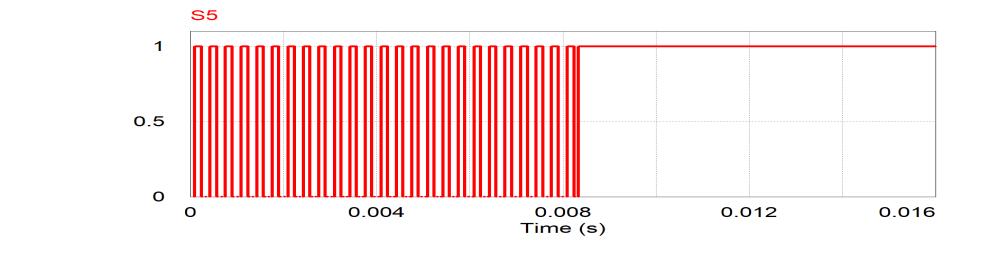
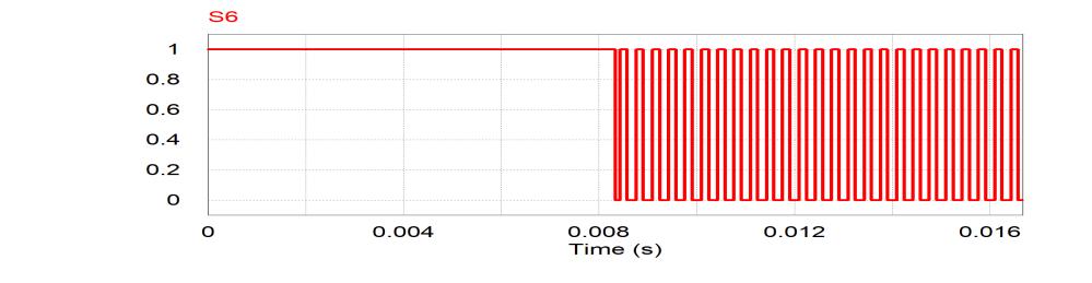
61 4.1.3 H6 Topology H6 topology is proposed in [44] and is derived from H5 topology by inserting an additional active switch in the negative bus of the DC kink, as shown in Figure 4.9. There are then six switches forming the structure of the H6 topology that are controlled independently. A unipolar SPWM modulation technique is used, Figure 4.10 shows the driving signals. There are four possible operating modes. In mode I, there are four switches conducting during the positive half cycle, which are S1, S4, S5, and S6. Two switches (S1, S6) are switched at the fundamental frequency and the other two switches (S4, S5) are switched at high switching frequency. Mode II is the freewheeling mode in the positive half cycle where current flows through S1 and the anti-parallel diode of S3. In mode III, four switches (S2, S3, S5, and S6) are conducting during the negative half period. In this mode, S2 and S5 are switched at the fundamental frequency; S3 and S6 are switched at high frequency. Mode IV is the freewheeling mode during the negative half period where the current flows through S3 and the antiparallel diode of S1. The inverter output voltage, common mode voltage VCM, and leakage current are presented in Figure Figure 4. 9 Circuit diagram of H6 topology 47

62 Figure Modulation strategy of H6 topology 48
63 Figure Common mode characteristics of H6 topology 49
64 4.1.4 H6-I Topology The H6-I topology is proposed in [49] and its structure and PWM strategy are presented in Figures 4.12 and There are four possible operating modes. During the positive active state, S1, S5, and S4 are conducting the positive output voltage. In the negative active state, switches S3, S6, and S2 are conducting the negative voltage to the output. Thus, a total of six switches are conducting in the active states. In the freewheeling mode, the DC source is disconnected from the grid and the current passes through only S5 and D1 to achieve zero output voltage in the positive zero state. In the negative zero state, the current path is established by S6 and D2 to obtain zero output voltage. The CM characteristics of the H6-I topology are shown in Figure It should be noted that H6-I topology has the same levels of leakage current and common mode voltage as those of H5 and H6. Figure Circuit structure of H6-I topology 50

65 Figure Switching waveforms of H6-I topology 51
66 Figure Common mode characteristics of H6-I topology 52
67 4.1.5 Proposed Topology The schematic diagram of the proposed topology is presented in Figure The proposed H6 topology is a modified version of conventional H6 topology. For the proposed topology, there are two switches conducting in the positive half cycle instead of the three of conventional H6 topology. By reducing the total number of conducting switches from six to five, there is a reduction in total conduction losses. There are four possible operating modes. The driving signals of the proposed topology are illustrated in Figure During the positive active state, S6 and S4 are connected to deliver positive output voltage, as illustrated in Figure 4.16(a). In the negative active state, S5, S3, and S2 are conducting, as presented in Figure 4.16(c). As noted, the total number of conducting switches during the active state is reduced from six to five switches. Consequently, the total conduction loss is reduced and system efficiency is improved. Figure 4.16(b) and Figure 4.16(d) show the freewheeling modes in the positive and negative half period during the zero state. In the positive zero state, the current passes through S1 and the body diode of S3 to achieve zero output voltage. In the negative zero state, current passes through S3 and the body diode of S1 to achieve zero output voltage. 53
68 Figure Circuit structure of the proposed topology (a) (b) (c) (d) Figure Operation modes of the proposed topology. (a) The positive active state; (b) the zero state during the positive half period; (c) the negative active state; and, (d) the zero state during the negative half period 54
69 Figure PWM strategy of the proposed topology 55
70 The CM characteristics of the proposed topology are shown in Figure It should be noted that the VCM is oscillating from 200V to 600 V and is not fixed to VDC/2. Also, the VAN and VBN are not flat at zero crossing because of the junction capacitances. Therefore, the leakage current is not completely eliminated. The simulated waveforms of grid current, grid voltage, and inverter output voltage are given in Figure Figure Common mode characteristics of the proposed topology 56
 Grid current; (b) grid voltage; and, (c) inverter")
71 (a) (b) (c) Figure Output waveform. (a) Grid current; (b) grid voltage; and, (c) inverter output voltage 57
72 4.2 Power Loss Analysis To evaluate the performance of PV transformerless inverters, it is important to measure the losses of the switching devices at different output loads. The losses in semiconductor power devices can be divided into two types: switching losses and conduction losses. A detailed power loss analysis of the semiconductor power devices and diode are given in [52]. To calculate the conduction losses, first the voltage drop across these devices must be identified as follows: v DS (MOSFET) = i(t) R DS (4.1) v CE (IGBT) = V t + i(t) R CE (4.2) v AK (Diode) = V f + i(t) R AK (4.3) Where VDS represents a drain to a source voltage drop of the MOSFET, RDS is the ON state resistance of the MOSFET, VCE is the voltage between collector and emitter in IGBT, Vt indicates the corresponding voltage drop under zero-current condition, RCE stands for the IGBT ON resistance, VAK represents the voltage between the anode and cathode of the diode, Vf denotes the diode corresponding voltage drop under zero-current condition, RAK is the ON resistance of the diode, and i(t) indicates the current passing through the device. The conduction losses can be calculated by the following equations: P Con act = 1 2π v cond i(t) D act (t)d( t) 0 π (4.4) i(t) = I m sin ( t + θ) (4.5) D act (t) = Msin( t) (4.6) 58
73 Where I m stands for the output current peak of the inverter, w represents the angular frequency, θ denotes the phase displacement between voltage and grid current, D act represents the duty ratio during, the active state and M can take a value between 0 and 1. The conduction loss of a single switching device in the zero state is expressed as: π P cond zero = 1 2π v con i(t)d zero (t)d( t) 0 (4.7) D zero (t) = 1 Msin( t) (4.8) Where Dzero represents the duty ratio during zero state. The second part of the power loss is the switching loss during turn-on and turn-off time. The switching ON and OFF power losses are given as: P ON = ( I m V DC 2π ) f E on sw (4.9) V test I test P OFF = ( I m V DC 2π ) f E off sw (4.10) V test I test Where Eon and Eoff are the turn-on and turn-off energy losses. These energy losses are measured under accurate test conditions over different junction temperatures and reported in data sheets for given values of switching current and voltage. The switching-on loss of a diode can be ignored because it is very small. The diode switching-off loss is calculated as follows: P Diode OFF = 1 12 t b I RRM V DC 2 f sw (4.11) Where IRRM denotes the reverse recovery current. 59
74 4.3 Total Losses and Performance Analysis PSIM simulation software was used to design and simulate the discussed various topologies. The thermal model also generated by the simulation software was used to calculate the switching and conduction losses and evaluate the system performance for the various topologies. The specifications of the system design are shown on Table 4.1. Table 4. 1 Specifications of the System Design Parameter Value Input Voltage Grid Voltage Grid Frequency Switching Frequency DC Bus Capacitor (CDC) Output Power 800 V 120 V 60 Hz 16 khz and 100 khz 970 µf 3 kw The switching and conduction losses at the rated power for different transformerless inverter topologies are presented in Figure It is noted that H6 has higher conduction loss and total losses because it has a total of four switches conducting during the positive and negative half cycle. The H4 with bipolar modulation has higher total losses than H5 and H6-I because there are four switches operating at the switching frequency during the positive and negative active states. The proposed topology has the lowest total losses compared to the other transformerless inverter topologies because the total number of conducting switches is reduced to five. 60
 for")
75 Figure Conduction and switching losses of various transformerless inverters at 16 khz [53] The efficiency of the various topologies is determined using the California Energy Commission (CEC) for different output power loads and is presented in Figure The efficiency is calculated according to the following: η CEC = 0.04η 10% η 20% η 30% η 50% η 75% η 100% (4.12) The calculated CEC for the bipolar H4, H5, H6, and H6-I and for the proposed topology are shown on Table
76 Table 4. 2 CEC Efficiency of Various Transformerless Inverters At 16 khz [53] Output Power (W) CEC Bipolar H % 92.5% 93.8% 94.7% 95% 95% 94.33% H5 94.8% 95.7% 95.9% 96% 95.9% 95.8% H6 94% 94.4% 94.8% 95.3% 95.1% 94.7% 95% H6I 95.6% 96.2% 96.47% 96.34% 96.2% 96% 96.2% Proposed Topology 95.8% 96.4% 96.8% 96.5% 96.4% 96.2% 96.4% Figure Efficiency comparison of various transformerless inverter topologies with different output power loads [53] 4.4 Conclusion This chapter presented a review of some of the recent advances in transformerless inverter topologies, such as H5, H6, and H6-I. All these topologies are modulated with unipolar SPWM to enhance system efficiency. Galvanic method isolation is used in these 62
77 topologies to solve the issue of leakage current. It is noted that leakage current is not completely eliminated because the common mode voltage is floating during the freewheeling period. A proposed transformerless inverter is introduced to increase system efficiency and reduce or eliminate leakage current. The number of conducting switches in the proposed topology is reduced from six to five switches. As a result, the total losses are reduced; the proposed topology also has the highest efficiency compared with the other reviewed topologies. 63
78 Chapter 5. Wide-Bandgap (WBG) Power Devices 5.1 Introduction Wide-bandgap (WBG) materials, such as silicon carbide (SiC), gallium nitride (GaN), and diamond can be excellent alternatives for Si material due to their superior properties, such as low ON state resistance, high switching speed, and high operating temperature. The first of the SiC-based devices to be launched was the SiC Schottky barrier diode; subsequently, this was followed by the introduction of fully controlled power semiconductor devices, such as the Metal Oxide Semiconductor Field Effect Transistor (MOSFET) and the Junction Field Effect Transistor (JFET) with a 600 V blocking voltage range. WBG power devices utilizing SiC and GaN offer superior conduction and switching performance compared to Si-based devices over a wide range of temperatures. Consequently, such WBG switching devices can be used to achieve high system efficiency and be promising solutions for highly efficient transformerless inverters. 5.2 Physical Characteristics of WBG Materials The main physical characteristics of the newer WBG device materials, such as SiC and GaN, and those of traditionally used Si material are presented on Table 5.1 [53] [64]. 64
79 Table 5. 1 Comparison of Physical Characteristics of Si, SiC, and GaN Material EG (ev) NI (cm -3 ) at 27 o C Dielectric constant (ɛr) EC (MV/cm) VSAT (10 7 cm/s) Si H-SiC GaN Where EG denotes the material bandgap, NI represents the intrinsic carrier concentration, ɛr is the relative permittivity, EC indicates the critical electrical field, and VSAT stands for the saturation velocity. The physical characteristics of WBG materials are analyzed and compared with the material traditionally used, silicon, to explain the superior performance of WBG-based power semiconductor devices in terms of: (a) high operating temperature, (b) lower ON-state resistance, and (c) higher switching speed Higher Operating Temperature Two physical characteristics are related to this feature: the lower intrinsic carrier concentration and the wider bandgap [66]. WBG materials have wider bandgap which means it needs high thermal energy to move the electron from the valence band to the conduction band. As a result, a higher temperature is required to trigger the electrons, a higher temperature which might lead to power device failure in devices made with silicon. In addition, WBG materials have a small value of intrinsic carrier concentration, which results in lower leakage current compared to Si-based devices at the same temperature. 65
80 5.2.2 Low ON-State Resistance The critical electrical field (EC) of WBG materials is almost more than 10 times higher than the EC of devices constructed with silicon material. Therefore, WBG-based power devices have lower ON-state resistance, according to the following equation [67]: R ON,SP = 4V BK 2 3 ɛ r µ n E (5.1) C Above, VBK denotes the device breakdown voltage, εs represents the relative permittivity, μn stands for the electron mobility, and EC is the critical electrical field. Clearly, there is an inverse relationship between the ON-resistance and the EC. Therefore, WBG-based power devices have much smaller ON-state resistance compared to Si-based devices. As a result, lower conduction losses are associated with WBG-based power devices due to this feature Higher Switching Speed Switching speed is related to two physical characteristics: saturation velocity (VSAT) and relative permittivity (ɛr). The VSAT of SiC and GaN is almost double the VSAT of silicon. Therefore, the electrons movement in WBG-based power devices is much faster than in Si-based power devices. In addition, WBG materials have lower relative permittivity compared to Si material. As a result, the parasitic capacitances of WBGbased power devices are smaller than those of Si-based power devices, leading to higher switching speed and transitions. 5.3 Loss Evaluation of Si IGBT and SiC MOSFET Power Devices The total power loss of a switching device can be classified in two ways, as a switching or a conduction loss. An accurate evaluation of conduction losses requires 66
![specific performance data obtained from a datasheet, such as the ON-state resistance of MOSFET, saturation voltages of IGBT, and forward voltage of body diode [68], [69].](/docs-images/92/108343331/images/81-1.jpg "Different parameters must be established for the evaluation of switching energy losses such as gate drive voltage, gate resistance, and junction temperature.")
81 specific performance data obtained from a datasheet, such as the ON-state resistance of MOSFET, saturation voltages of IGBT, and forward voltage of body diode [68], [69]. Different parameters must be established for the evaluation of switching energy losses such as gate drive voltage, gate resistance, and junction temperature. A double pulse test circuit was designed using LTSpice for both switching devices to create an accurate comparison of switching energy losses as shown in Figure 5.1. Figure 5. 1 Double Pulse Test Circuit Evaluation of Conduction Losses Conduction losses can be determined by multiplying the voltage drop across the switch when it is ON with current flowing through. Conduction losses represent a major portion of total overall semiconductor losses. The stated forward voltages of the selected switching power devices over different current values are given in Figure 5.1(a) and Figure 5.1(b). It was noted that the SiC MOSFET has a small voltage drop as compared to that of the Si IGBT due to the resistive output characteristics of the SiC MOSFET, which leads to a reduction in conduction losses. 67
82 (a) (b) Figure 5. 2 (a) Forward voltages of SiC MOSFET and Si IGBT at 25 ; and, (b) forward voltages of SiC MOSFET and Si IGBT at Evaluation of Switching Losses LTspice software was used to study the switching waveform characteristics of the selected switching power devices. The models used with the software were provided by the manufacturers of the devices. The turn-on and turn-off switching waveforms at 800 V and 30 A for SiC MOSFET and Si IGBT are shown in Figure 5.2. Clearly, the SiC MOSFET has better switching characteristics in terms of dv/dt and di/dt. At the turn- OFF transition, the dv/dt is measured for both switching devices. It was also found that SiC MOSFET switches at the much higher 19.8 kv/ms while the Si IGBT switches at 3.9 kv/ms. Table 5.2 presents the turn-on and turn-off transition states for both switching devices. 68

 Turn-ON SiC MOSFET; (b) turn-on Si IGBT; (c)")
83 (a) (b) (c) (d) Figure 5. 3 Switching transitions of switching devices for a voltage of 800 V and 30 A. (a) Turn-ON SiC MOSFET; (b) turn-on Si IGBT; (c) turn-off SiC MOSFET; and, (d) turn-off Si IGBT 69
84 Table 5. 2 Turn-ON and turn-off switching transition dv dt (kv μs ) Turn-on Turn-off Si IGBT SiC MOSFET Si IGBT SiC MOSFET di dt (ka μs ) The switching energies can be calculated by taking the integral of the product of the voltage and current. By applying this method, the measured turn-on and turn-off energies of both switching devices are given in Figure 5.3. The turn-on switching energy losses are small compared to the turn-off switching energy losses for both switching devices. The study shows that at low current levels, the Si IGBT must dissipate more than three times the turn-on energy of the SiC MOSFET. Therefore, the switching energy losses of Si IGBT are much greater and increase linearly with the current. However, SiC MOSFET has very low turn-off energy losses, which can be a major advantage compared to Si IGBT. Also, the total energy loss of SiC MOSFET increases slightly when the temperature is increased to 100. The turn-off energy losses of the Si IGBT are about eight times higher than SiC MOSFET at a current of 6 A and about 10 times higher at a current of 30 A, as shown in Figure 5.3(b). The drawback of Si IGBT is that it has large switching energy losses. As a result, SiC MOSFET is an attractive solution for high switching frequency application because of its superior switching characteristics. 70
85 (a) (b) (c) (d) Figure 5. 4 Turn-ON and turn-off switching energy losses for 800 V and 30 A. (a) Turn- ON energies at 25 ; (b) turn-off energies at 25 ; (c) turn-on energies at 100 ; and, (d) turn-off energies at
86 5.4 Conclusion The physical properties of WBG materials such as SiC and GaN are described in this chapter. WBG materials have certain superior characteristics compared to those of Si material, such as wider bandgap, low intrinsic carrier concentration, and high saturation velocity. As a result, WBG-based semiconductor devices can operate at high temperature, have low ON-state resistance, and operate at high switching frequency. Moreover, a double pulse test circuit designed in LTspice to evaluate and simulate the dynamic and static characteristics of two switching devices, SiC MOSFET and Si IGBT, at 1200V blocking voltage found that SiC MOSFET also has low switching and conduction losses compared to those of Si IGBT. 72
87 Chapter 6. Benefits of SiC MOSFET in PV System 6.1 Introduction The benefits of using WBG power devices, such as SiC MOSFET, are discussed in detail in this chapter. WBG power devices can operate at high switching frequencies and have low switching and conduction losses due to their material properties [70], [71]. Therefore, a high system efficiency and high-power density can be achieved with WBG power devices such as SiC MOSFET and GaN HEMT [72] [76]. The benefits of utilizing SiC MOSFET instead of Si IGBT are studied and demonstrated in this section. 6.2 Performance Enhancement of the Proposed High Gain DC-DC Converter Using SiC MOSFET The performance of the system is enhanced by using WBG power devices such as SiC MOSFET. Two types of switching power devices are used in this study, SiC and Si MOSFET, to compare their switching and conduction losses at high switching operating frequencies. The specifications of these two types of devices are shown in Table
88 Table 6. 1 Specifications of the switching devices Parameter Breakdown Voltage Si MOSFET TK35A65W5 650V SiC MOSFET SCT3060AL 650V Continuous Current 35A 39A RDS-ON 80mΩ 60mΩ Qrr 780nC 55nC Trr 130ns 15ns Conduction and switching losses of Si and SiC MOSFET at different switching frequencies and output power of 2 kw are presented in Figure 6.1. The results show that the conduction losses of the proposed converter were reduced by 65% with SiC MOSFET. This reduction in conduction losses is due to the smaller ON state resistance of SiC MOSFET. Also, switching losses at 100 khz were reduced by about 90% with SiC MOSFET. The reverse recovery charge of Si MOSFET is about 14 times greater than that of SiC MOSFET. Moreover, the reverse recovery time of Si MOSFET is approximately nine times greater than SiC MOSFET. This explains the large switching losses of Si compared to those of SiC MOSFET. 74

89 Figure 6. 1 Conduction and switching losses of Si and SiC MOSFET at different switching frequencies [33] Switching losses of the system at 200 khz are reduced by around 90% with SiC MOSFET, which is a significant reduction in switching losses. Compared with switching losses at 100 khz, switching losses of SiC MOSFET is increased by only 3.5 W while the switching losses of Si MOSFET increased by 30.5 W. Figures 6.2, 6.3, and 6.4, demonstrate the efficiency of the system with different output power loads at different switching frequencies. At 100 khz, the efficiency of the system improved by two percent. Moreover, the efficiency increased by 3% when the switching frequency increased to 200 khz. The advantages to using SiC MOSFET became even more obvious at a higher switching frequency where the efficiency increased by 4% at 300 khz. Furthermore, it was observed that the power rating of the system can be increased from 200 W to 2000 kw for the same total losses at a switching frequency of 100 khz. 75
90 Figure 6. 2 Efficiency comparison of Si and SiC MOSFET at 100 khz with different output power loads [33] Figure 6. 3 Efficiency comparison of Si and SiC MOSFET at 200 khz with different output power loads [33] 76
91 Figure 6. 4 Efficiency comparison of Si and SiC MOSFET at 300 khz with different output power loads [33] 6.3 Benefits of SiC MOSFET in the Proposed Transformerless Inverter The benefits of implementing SiC MOSFET instead of Si IGBT are studied and demonstrated in this section. The parameters of the selected switching devices are given on Table 6.2. Table 6. 2 Parameters of selected switching devices Parameter IGBT (FGH15T120SMD) SiC (C2M D) Breakdown Voltage (V) Continuous Current (A) RDS-ON/RCE (mω) Vt (V) Vf (V) RAK (mω) IRRM (A) Qrr (reverse recovery charge) (nc) Trr (reverse recovery time) (ns)
92 6.3.1 Efficiency Improvement Semiconductor losses have a significant impact on inverter efficiency. The semiconductor losses for Si IGBT and SiC MOSFET over different output power loads at 16 khz are presented in Figure 6.5(a). It is observed that SiC MOSFET has low conduction losses at light loads because of its resistive output characteristics. Moreover, at a full output power load of 3 kw, the conduction losses of the Si IGBT are almost the same as those of SiC MOSFET because Si IGBT has a constant voltage drop. On the other hand, the major benefit to using SiC MOSFET is its low switching losses due to the absence of tail current. The total losses are reduced by more than 50% with SiC MOSFET. The semiconductor losses with different output power loads at 100 khz are given in Figure 6.5(b). The total power loss of the Si IGBT at 100 khz is about four times greater than that at 16 khz, which means that Si IGBT is not suitable for high switching frequency applications. On the other hand, the total power loss of SiC MOSFET is increased by only 12% at 100 khz. 78
93 (a) (b) Figure 6. 5 Conduction and switching losses of Si IGBT and SiC MOSFET with different output power loads. (a) at 16 khz; and, (b) at 100 khz. [53] The efficiency of the system with different output power loads at two different switching frequencies is illustrated in Figure 6.6. The efficiency of the system at 16 khz is increased by 2% with SiC MOSFET. The benefits of using SiC MOSFET become more obvious at higher switching frequencies where the efficiency of the system increases by almost 14% at 100 khz compared to the efficiency of Si IGBT at the same level. 79
94 Figure 6. 6 Efficiency comparison between Si IGBT and SiC MOSFET with different output power loads and at two different switching frequencies [53] Switching Frequency vs. Inductor Volume The simulation results verified that SiC MOSFET can operate at high switching frequency while maintaining low power losses. The value of the inductor is inversely proportional to the switching frequency as shown in the following equation. L = V DC 4 f sw i max i ripple (6.1) Where VDC is the DC bus voltage, fsw denotes the switching frequency, imax is the peak current, and Δiripple is the current ripple and set as 20% of the peak current. A significant reduction in the inductor volume can be achieved when the switching frequency increases to higher values. In this study, it was found to be possible to increase the switching frequency of the proposed SiC MOSFET system all the way to 200 khz until the power losses matched those found in the Si IGBT system at only 16 khz, as shown in Figure
95 The inductor value at different switching frequencies is presented in Figure 6.8 where it is shown that it decreased from 1400 µh at 20 khz to 140 µh at 200 khz. The large reduction in the inductor value leads to small size and volume of inductor storage. The core material used in this study, for the sake of comparison, was a toroid core manufactured using Kool Mu material. The effect on the magnetic core volume of increasing the switching frequency is presented in Figure 6.9. This study shows that, as the switching frequency increases, the magnetic core volume decreases. The magnetic core volume decreased from 220 cm 3 at 20 khz to 20.7 cm 3 at 200 khz. Moreover, a smaller inductor volume leads to smaller inductor weight. The relationship between the switching frequency and the inductor weight is shown in Figure The inductor weight is reduced from 1200 g at 20 khz to 120 g at 200 khz. Figure 6. 7 Switching frequency vs. power losses for SiC MOSFET and Si IGBT [53] 81
96 Figure 6. 8 Switching frequency vs. inductor values [53] Figure 6. 9 Switching frequency vs. magnetic core volume [53] 82
97 Figure Switching frequency vs. inductor weight [53] Increasing Power Rating As explained previously, using SiC MOSFET instead of Si IGBT leads to a significant reduction in total power losses. Therefore, the power rating of the inverter could be increased by adding more power to the load without modifying the size of the heat sink. The output of the inverter can be increased from 1.7 kw using Si IGBT to 3 kw using SiC MOSFET for the same total power semiconductor losses, as illustrated in Figure In other words, the power rating of the system can be increased by more than 75% with SiC MOSFET. 83
98 Figure Increased power rating with SiC MOSFET for the same power semiconductor losses [53] 6.4 Thermal Model Simulation and Heat Sink Design The use of simulation software for modelling thermal performance of heat sinks is not a new practice and has been reported on in the literature [77] [81]. Commercial software -- like COMSOL Multiphysics, FLUENT, ANSYS, Pro-MECHANICA, etc. -- are prime examples of simulation software that use numerical methods, Finite Element and Finite Volume Methods (FEM and FEV), along with Computer Aided Design (CAD) tools to model the thermal performance of heat sinks. For the purposes of this paper, COMSOL Multiphysics was used to create two identical 3D models of a 6-pack MOSFET module with silicon (Si) and silicon carbide (SiC) as their respective semiconductor materials. Heat sinks were added to these MOSFET modules to reduce the structures temperatures and to compare each semiconductor s thermal performance. COMSOL solved for the temperatures of the 3D structure using Finite Element Analysis (FEA). Boyd Corp s online tool, AAVID Genie, 84
99 was used to verify the results of the simulated structures with their commercially available heat sinks that were simulated in COMSOL. The Heat Transfer in Solids module of COMSOL simulated the thermal aspects of the models. The Joule heating generated by electric currents passing through each of the MOSFET modules were obtained from calculations made in PowerSim, which were used as the heat sources for the COMSOL calculations. A stationary study was created for each model to study the steady state effects of the Joule heating on the temperature of each structure. The physical dimensions of both MOSFET modules were kept the same and were obtained from the CREE 1200V, 50A 3-Ph SiC MOSFET module [81]. The dimensions of the heat sink for the SiC model were made smaller to demonstrate the superiority of the widebandgap (WBG) material SiC in terms of heat sink requirements for similar steady state temperatures. For the purposes of this paper, thermal stresses and physical deformation were not simulated Model Geometry The internal structure the CREE 1200V, 50A 3-Ph SiC MOSFET module consists of multiple layers and components. The dimensions of this internal structure were obtained from [82] to create the 3D CAD model of the module in COMSOL. The module starts from the bottom to the top with a copper (Cu) Baseplate, a solder layer, a copper layer, an aluminium nitride (AlN) layer, and then another copper layer [82]. Six sets of MOSFETs and diodes are soldered on top of the final copper layer [82]. The dimensioned 3D view, the yz-plane view, and the xy-plane view of the MOSFET modules are shown in Figures 6.12, 6.13, and 6.14, respectively. Figure 6.13 is scaled so 85


100 that all the layers are viewable. The MOSFETs and diodes were set to be of the same semiconductor material, i.e., Si and SiC, for their respective models. Figure D View of MOSFET module Figure yz-plane view of the module 86

101 Figure xy-plane view of the module The final layer of each model consists of an aluminium (Al) heat sink which rests on top of the MOSFET and diode layers. The dimensions of the heat sinks were obtained from Boyd Corporation s online tool, AAVID. These dimensions were based on real world heat sinks sold by Boyd Corp. that would make the maximum temperatures of the module-heat sink combinations below 100º C. The heat sinks used for the Si and SiC modules are shown in Figures 18(a) and 18(b), respectively. Each heat sink consists of a solid aluminium block with the dimensions: mm mm. 6.6 mm. A total of 16 aluminum fins (width of mm) separated by 6.8 mm were added on top of this block with heights of 33.5 mm and 13.4 mm for the Si and SiC models, respectively. 87
, and thermal conductivity (k).")
.")
102 (a) (b) Figure Heat sink structure. (a) Si model; and (b) SiC model Material Properties The physical material properties of both models were Density ρ, heat capacity at constant pressure (cp), and thermal conductivity (k). Only these three properties were used for the simulations because heat transfer in solids was the only physics being studied. The materials were assumed to be isotropic with every property considered to be constant in all three directions (xyz). The properties for all materials simulated in the models, except for the solder, were obtained from built-in libraries in COMSOL. SAC396 solder, an alloy of tin, silver and copper, was chosen for the models and its 88
103 properties were obtained from [83]. The material properties for all the materials used are given in Table 6.3. Table 6. 3 Thermal properties of materials used Property Symbol Unit Cu SA AIN Si SiC Al C396 Density ρ kg/m Heat Capacity at Constant Pressure Cp J/(kg.K) Thermal Conductivity k W/(m.K) Heat Transfer Physics Modelling The heat transfer in the solids physics module of COMSOL was used to simulate the thermal performance of each MOSFET-heat sink structure. The heat losses calculated in PowerSim for each MOSFET in each semiconductor model were input as heat sources for the simulations. For the Si model, these losses, going from left to right were: W, W, W, W, 20.4 W, and 20.4 W; for the SiC, the losses were: 4.1 W, 4.1 W, 4.1 W, 4.1 W, W, and W, respectively. As the heat sinks dissipate, thermal energy from the heat generated by the MOSFETs to the surrounding air, a convective heat flux boundary condition for all heat sink surfaces in contact with that air was set up. The convective heat transfer coefficient was given a value of W/m 2.K to simulate non-forced free flowing air. The initial temperature of the structures and surrounding air was set to room temperature (i.e., K or 20º C). Using these inputs and boundary conditions, COMSOL solved the heat equation in solids to obtain the temperature profiles of each model. 89
 (b) Figure 6.")
104 6.4.4 Model Simulation and Results The temperature profile of the Si and SiC models with the heat sinks hidden are shown in Figure 6.16(a) and Figure 6.16(b). The temperature profiles for the Si and SiC models with the heat sinks visible are given in Figures 6.17 and The temperatures displayed on the legends are in Celsius. (a) (b) Figure Temperature profile of SiC model with heat sink not visible. (a) Si; and, (b) SiC. [53] 90
105 The temperature profiles for the Si and SiC models with the heat sink not visible show that the highest of temperatures are concentrated around the MOSFETs that have the highest heat losses. As the heat losses for all Si IGBTs are close to 20 W, the temperatures are fairly uniform throughout the Si MOSFET module structure whereas for the SiC model, the temperatures are higher at the right end near the MOSFETs with losses of W losses while the left end with lower losses has lower temperatures. The temperature profiles for the two models with the heat sink visible also show a similar distribution of temperatures. The Si model has higher temperatures on the heat sink that are fairly uniform around all the IGBTs, while the SiC model has higher temperatures more concentrated at the right end where the MOSFETs with higher losses are located. Figure Temperature profile of Si model with heat sink visible [53] 91
![Figure 6. 18 Temperature profile of SiC model with heat sink visible [53] The maximum temperatures for the Si and SiC models were found to be 95.15 ºC and 90.18 ºC respectively.](/docs-images/92/108343331/images/106-0.jpg "The minimum temperatures were 76.23 ºC and 76.10 ºC for the Si and SiC models, respectively. The 3D model for the Si IGBTs had a volume of 183.8 cm 3 and surface area of 1,861 cm 2 for the heat sink.")
106 Figure Temperature profile of SiC model with heat sink visible [53] The maximum temperatures for the Si and SiC models were found to be ºC and ºC respectively. The minimum temperatures were ºC and ºC for the Si and SiC models, respectively. The 3D model for the Si IGBTs had a volume of cm 3 and surface area of 1,861 cm 2 for the heat sink. The SiC model had a volume of cm 3 and surface area of cm 2. From the simulations of the two models, it is clear that the SiC MOSFET module requires a smaller heat sink (by a factor of.505 or approximately half - in terms of surface area) for similar maximum temperatures. High temperatures are more uniform in the Si model while only the areas with higher losses have areas of high temperature concentrations throughout the overall volume of the MOSFET module with SiC. The thermal modelling clearly demonstrates that the SiC module is more efficient in terms of heat sink size and overall heat dissipation. 92
107 6.5 Conclusion The benefits of using WBG-based power devices, such as SiC MOSFET is investigated in this chapter. The benefits of using SiC MOSFET at 650 V blocking voltage is investigated in the proposed high gain boost converter and compared to those of Si MOSFET. The simulation results show that switching and conduction losses are reduced by more than 90% and 65%, respectively, with SiC MOSFET. Also, the efficiency of the system improved by more than 4% with SiC MOSFET at a high switching frequency of 300 khz. Next, the benefits of using SiC MOSFET at 1200 V blocking voltage is studied in the proposed transformerless inverter and compared to those of using Si IGBT. The simulation results show that total switching and conduction losses are reduced by 50% at 16 khz and the efficiency increased from 96% to 98% with SiC MOSFET. The benefits of using SiC devices become more obvious at a high switching frequency of 100 khz where the efficiency increases by about 14%. The significant reduction of the total switching and conduction losses opens the possibility of increasing the inverter power rating level with SiC MOSFET. For example, the power rating of the inverter at 16 khz with Si IGBT is increased by 75%, from 1.7 kw to 3 kw, with the same power losses when SiC MOSFET is used. Furthermore, SiC MOSFET has superior switching characteristics, which allow the system to increase its switching frequency by a factor of 15 while still having the same power semiconductor losses as an Si IGBT based inverter. By taking advantage of this fact, the volume and weight of the inductor filter may be reduced dramatically from 220 cm 3 to 20.7 cm 3 and from 1.2 kg to 120 g, respectively. Finally, thermal analysis shows that SiC MOSFET requires smaller 93
108 heat sink compared to Si IGBT under the same switching frequency and output power load. Accordingly, SiC devices are an attractive solution for residential PV applications that require high efficiency and small converter size. 94
109 Chapter 7. Improved Proposed Converter for Reactive Power Generation and Leakage Current Elimination 7.1 Introduction Several transformerless inverter topologies have been presented and published [83] [85]. One of the drawbacks of PV transformerless inverters is the generating of leakage current due to the absence of a transformer. High generation of leakage current increases system losses, THD, electromagnetic interference (EMI), and can cause personal safety issues [86] [93]. The literature cites various modulation techniques that have been used to eliminate or minimize leakage current. Many transformerless inverter topologies with unipolar modulation technique have been introduced to increase system efficiency and reduce the leakage current by disconnecting the AC and DC sides during the freewheeling modes, this is known as galvanic isolation. Many topologies have been derived and developed based on this method, including highly efficient and reliable inverter concept (HERIC), the H5 inverter, and the H6 topology [94], [95]. However, complete elimination of leakage current cannot be achieved with galvanic isolation method alone because common mode voltage (CMV) during freewheeling periods cannot be identified by the switching state, which means that it is not constant. Therefore, modulation strategies and converter structures must be modified so that CMV becomes constant during all inverter operating modes. 95
110 Most of the modulation techniques are designed for the application of a unity power factor. Indeed, next-generation PV inverters are required to support reactive power to allow for the high penetration of PV inverters to be connected to the utility grid [96] [99]. Several international standards have been reviewed to achieve reactive power support. As reported by VDE-AR-N4105, PV grid connected inverters must have the ability to generate reactive power. Considering all this, a traditional bipolar modulation technique is proposed as a possible candidate to be used in next-generation PV inverters, because it has the ability to generate reactive power and eliminate leakage current. Nevertheless, using bipolar modulation techniques to generate reactive power will increase switching losses and degrade system efficiency as it is a two-level modulation. The Si MOSFET based transformerless inverter is highly efficient in generating reactive power, but the inverter design must be optimized to address the fact that the Si MOSFET s body diode has poor reverse recovery performance, which may lead to device failure [100] [103]. These inverters are based on the idea of avoiding the conduction of an anti-parallel diode, which will result in a more complicated and complex inverter that in turn increases costs. On the other hand, the SiC MOSFET s body diode has superior reverse recovery performance because it has a shorter minority carrier lifetime [104] [113]. Therefore, reactive power generation with SiC MOSFET can be achieved without any alteration to the converter structure or adding any additional freewheeling diodes (FWD). 96
111 7.2 Proposed Topology with Leakage Current Elimination and Reactive Power Generation The proposed H6 topology is derived from conventional H6 topology where the sixth switch is repositioned and connected to the A terminal [114] [115]. The proposed topology and its switching pattern are presented in Figures 7.1 and 7.2. The proposed topology has low conduction loss compared to traditional topologies, such as H5 and H6, because the number of conducting switches is reduced from six switches to five switches. On the other hand, only using galvanic isolation will not maintain the desired constant CMV during the freewheeling period. Since the inverter output terminals A and B are floating during the freewheeling periods with respect to DC side, this means that CMV cannot be determined from the switching states. Accordingly, generation of leakage current cannot be fully controlled with the galvanic isolation method. Therefore, the proposed topology is improved by incorporating clamped method technique to eliminate the leakage current and achieve constant CMV during the freewheeling period, as shown in Figure 7.3. The dc link capacitor is divided into two series capacitors to achieve voltage divider. In the clamping method, an extra active switch is added to the proposed topology. This switch is known as a clamping switch and is placed between the midpoint of the freewheeling switches and the midpoint of the dc link capacitors. The generation of reactive power cannot be accomplished in single phase transformerless inverter topologies because the existing modulation techniques are not adopted for a freewheeling path in the negative power region. To use unipolar PWM in the negative power region, the line to line voltage (VAB) must have three values, + VDC, - 97

112 VDC, and zero. It is observed that zero voltage states cannot be achieved in the negative power regions because there is no current path established, as illustrated in Figure 7.4. The modulation method is modified to achieve leakage current elimination and reactive power generation, as shown in Figure 7.5. Figure 7. 1 Circuit diagram of proposed transformerless inverter topology Figure 7. 2 Modulation strategy of the proposed transformerless inverter 98
113 Figure 7. 3 Modified proposed transformerless inverter [116] (a) Figure 7. 4 Operation modes of the negative power region during freewheeling periods. (a) Vg is positive and Ig is negative; and, (b) Vg is negative and Ig is positive (b) 99

.")
114 Figure 7. 3 Modified modulation strategy for leakage current elimination and reactive power generation 7.2 Modulation Technique for Reactive Power Generation The proposed PWM modulation technique divided into four regions and eight modes, as shown in Figure 7.5. In regions II and IV, the power is positive where Ig and Vg have the same polarity. The power is negative in regions I and III where Ig and Vg have an opposite sign. The operation modes are described as follows. Mode-I is the active mode in the positive power region (both Ig and Vg are positive). In this mode, S1, S6, and S4 are turned ON, and the other switches are turned OFF, as shown in Figure 7.6(a). The inductor current is flowing through S4 and S6. The common mode voltage in Mode-I is calculated as follows: v AN = V PV (7.1) v BN = 0 (7.2) v CM = v AN + v BN 2 = 0.5V PV (7.3) Mode-II is the freewheeling mode in the positive power region (both Ig and Vg are positive). In this mode, S1, S3, and S7 are turned ON and the other switches are turned 100
115 OFF, as shown in Figure 7.6(b). The inductor current is flowing through S1 and the antiparallel diode of S3. The common mode voltage in Mode-II is given as: v AN = v BN = 0.5V PV (7.4) v CM = v AN + v BN 2 = 0.5V PV (7.5) (a) (b) Figure 7. 4 Operation modes of the proposed topology. (a) Ig and Vg are positive; and, (b) the zero state during this interval 101
116 Mode-III is the active mode in the positive power region (both Ig and Vg are negative). In this mode, S5, S3, and S2 are turned ON and the other switches are turned OFF as shown in Figure 7.7(a). The inductor current is flowing through S2, S3, and S5. The common mode voltage in Mode-III is expressed as: v AN = 0 (7.6) v BN = V PV (7.7) v CM = v AN + v BN 2 = 0.5V PV (7.8) Mode-IV is the freewheeling mode in the positive power region (both Ig and Vg are negative). In this mode, S1, S3, and S7 are turned ON and the other switches are turned OFF, as shown in Figure 7.7(b). The inductor current is flowing through S3 and the antiparallel diode of S1. The common mode voltage in Mode-IV is calculated as follows: v AN = v BN = 0.5V PV (7.9) v CM = v AN + v BN 2 = 0.5V PV (7.10) 102
117 (a) Figure 7. 5 Operation modes of the proposed topology. (a) Ig and Vg are negative; and, (b) the zero state during this interval (b) Mode-V is the active mode in the negative power region (Ig is positive and Vg is negative). In this mode, S4 and S6 are OFF, while S2, S5, and S3 are ON; thus, inductor current freewheels through the anti-parallel diodes of S2, S5, and S3, as given in Figure 7.8(a). V CM is determined as: v AN = 0 (7.11) v BN = V PV (7.12) v CM = v AN + v BN (7.13) = 0.5V 2 PV Mode-VI is the freewheeling mode in the negative power region (Ig is positive and Vg is negative). In this mode, S1 commutates complementary to S2 and S5 at the 103
118 switching frequency instead of being OFF for the whole negative period as in the conventional unipolar PWM modulation. In this arrangement, a new current path is created to generate zero-voltage by turning OFF S2, S4, S5, and S6 and turning ON S1, S3, and S7. Thus, the inductor current passes over S1 and the antiparallel diode of S3 as depicted in Figure 7.8(b). V CM is determined as: v AN = v BN = 0.5V PV (7.14) v CM = v AN + v BN 2 = 0.5V PV (7.15) (a) Figure 7. 6 Operation modes of the proposed topology. (a) Vg is positive and Ig is negative; and, (b) the zero state during this interval (b) 104
119 Mode-VII is the active mode in the negative power region (Ig is negative and Vg is positive). In this mode, S2, S5, and S3 are OFF while S4, S6, and S1 are ON; thus, inductor current freewheels through the anti-parallel diodes of S4 and S6, as shown in Figure 7.9(a). V CM is determined as: v AN = V PV (7.16) v CM = v AN + v BN 2 v BN = 0 (7.17) = 0.5V PV (7.18) Mode VIII is the freewheeling mode in the negative power region (Ig is negative and Vg is positive). In this mode, S3 commutates complementary to S4 and S6 at the switching frequency instead of being OFF for the whole positive period, as in the conventional unipolar PWM modulation. In this arrangement, a new current path is created to generate zero-voltage by turning OFF S2, S4, S5, and S6 and turning ON S1, S3, and S7. Thus, the inductor current passes over S3 and the antiparallel diode of S1 as depicted in Figure 7.9(b). V CM is determined as: v AN = v BN = 0.5V PV (7.19) v CM = v AN + v BN 2 = 0.5V PV (7.20) 105
120 (a) Figure 7. 7 Operation modes of the proposed topology. (a) Vg is negative and Ig is positive; and, (b) the zero state during this interval (b) By implementing the proposed modulation, a new current path is created in region II and IV to achieve a zero-voltage state. Therefore, the three output voltages generated +VDC, 0, and -VDC, which satisfy the principle operation of unipolar PWM modulation technique. The main concept of the proposed modulation technique is to create a bidirectional current path of S1 and S3 during the negative power region. As a result, reactive power generation can be achieved with the proposed modulation technique. Moreover, the proposed modulation technique maintains a constant common mode voltage at VDC/2 over all the operation modes, which will result in eliminating leakage current. Consequently, the proposed H6 topology with the modified unipolar PWM 106
121 modulation technique is suitable for the next generation of PV transformerless inverter applications. 7.3 Simulation Results PSIM and MATLAB/SIMULINK simulation software programs were used to design the proposed topology to evaluate its performance. The parameters of the system design are shown on Table 7.1. The simulation included two switching frequencies: 16 khz and 100 khz. Table 7. 1 System Design Parameters Parameter Input Voltage Grid Voltage Grid Frequency Switching Frequency Value 800 V 120 V 60 Hz 16 khz and 100 khz DC Bus Capacitor (CDC) 970 µf Stray Parasitic Capacitance Output Power 300 nf 3kW The CM characteristics of the proposed topology, with only galvanic isolation, are given in Figure

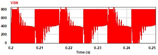
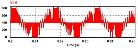

122 Figure 7. 8 CM characteristics of the proposed topology 108
123 It is observed that the voltage waveforms of VAN and VBN are oscillating. Also, the common mode voltage VCM is oscillating and not constant at 400 V. Therefore, there is a flow of leakage current that cannot be eliminated. To resolve this problem, the proposed topology is modified with a clamping method and the CM characteristics, such as VAN, VBN, VCM and ILeakage, that are shown in Figure It is also noted that the voltage waveforms of VAN and VBN are smooth and complementary to each other. As a result, the VCM is totally clamped to 400 V over the whole period, which will lead to a total elimination of leakage current. 109


124 Figure 7. 9 CM characteristics of the modified proposed topology [116] 110
125 The simulated waveform of the proposed H6 inverter at unity power factor with traditional and proposed unipolar PWM modulation is presented in Figure Both modulation techniques are expected to perform properly for purely active power of a unity power factor. On the other hand, with non-unity power factor (reactive power generation) the traditional unipolar PWM does not work correctly. Figure 7.13 shows a current distortion in the negative power region because there is no current path to realize a zero-voltage through the negative power region. However, the issue of current distortion with conventional unipolar PWM can be resolved with the proposed unipolar PWM. The proposed modulation technique works optimally with lagging or leading power factor where the simulated waveform has free current distortion as depicted in Figure Hence, the proposed modulation technique supports the proposed H6 inverter for reactive power generation. (a) (b) Figure Vg and Ig for the proposed H6 inverter under unity power factor. (a) Traditional unipolar PWM; and, (b) proposed unipolar PWM [116] 111
![Figure 7. 11 Grid current for the proposed inverter under non-unity power factor with conventional unipolar PWM [116] Figure 7.](/docs-images/92/108343331/images/126-2.jpg "12 Grid current for the proposed inverter under non-unity power factor with modified conventional unipolar PWM [116] Figure 7.")
126 Figure Grid current for the proposed inverter under non-unity power factor with conventional unipolar PWM [116] Figure Grid current for the proposed inverter under non-unity power factor with modified conventional unipolar PWM [116] Figure Total harmonic distortion (THD) of the proposed topology with conventional and modified modulation technique [116] 112
IMPROVED TRANSFORMERLESS INVERTER WITH COMMON-MODE LEAKAGE CURRENT ELIMINATION FOR A PHOTOVOLTAIC GRID-CONNECTED POWER SYSTEM
 IMPROVED TRANSFORMERLESS INVERTER WITH COMMON-MODE LEAKAGE CURRENT ELIMINATION FOR A PHOTOVOLTAIC GRID-CONNECTED POWER SYSTEM M. JYOTHSNA M.Tech EPS KSRM COLLEGE OF ENGINEERING, Affiliated to JNTUA, Kadapa,
Analysis and comparison of two high-gain interleaved coupled-inductor boost converters
 Scholars' Mine Masters Theses Student Research & Creative Works 2015 Analysis and comparison of two high-gain interleaved coupled-inductor boost converters Venkat Sai Prasad Gouribhatla Follow this and
Design And Analysis Of Dc-Dc Converter For Photovoltaic (PV) Applications.
 Applications.") IOSR Journal of Engineering (IOSRJEN) ISSN (e): 2250-3021, ISSN (p): 2278-8719 PP 53-60 www.iosrjen.org Design And Analysis Of Dc-Dc Converter For Photovoltaic (PV) Applications. Sangeetha U G 1 (PG Scholar,
IOSR Journal of Engineering (IOSRJEN) ISSN (e): 2250-3021, ISSN (p): 2278-8719 PP 53-60 www.iosrjen.org Design And Analysis Of Dc-Dc Converter For Photovoltaic (PV) Applications. Sangeetha U G 1 (PG Scholar,
Transformerless Grid-Connected Inverters for Photovoltaic Modules: A Review
 International Journal of Engineering and Technical Research (IJETR) ISSN: 2321-869, Volume 3, Issue 4, April 215 Transformerless Grid-Connected Inverters for Photovoltaic Modules: A Review Sushant S. Paymal,
Improved H6 Transformerless Inverter for PV Grid tied power system
 Improved H6 Transformerless Inverter for PV Grid tied power system Madhuri N.Kshirsagar madhuri.n.kshirsagar@gmail.com Pragati K. Sharma pragatisharma91@gmail.com Shweta A. Deshmukh shweta4155@gmail.com
International Journal of Engineering Science Invention Research & Development; Vol. II Issue VIII February e-issn:
 ANALYSIS AND DESIGN OF SOFT SWITCHING BASED INTERLEAVED FLYBACK CONVERTER FOR PHOTOVOLTAIC APPLICATIONS K.Kavisindhu 1, P.Shanmuga Priya 2 1 PG Scholar, 2 Assistant Professor, Department of Electrical
An Interleaved Flyback Inverter for Residential Photovoltaic Applications
 An Interleaved Flyback Inverter for Residential Photovoltaic Applications Bunyamin Tamyurek and Bilgehan Kirimer ESKISEHIR OSMANGAZI UNIVERSITY Electrical and Electronics Engineering Department Eskisehir,
Analysis and Design of Solar Photo Voltaic Grid Connected Inverter
 Indonesian Journal of Electrical Engineering and Informatics (IJEEI) Vol. 3, No. 4, December 2015, pp. 199~208 DOI: 10.11591/ijeei.v3i4.174 199 Analysis and Design of Solar Photo Voltaic Grid Connected
Generalized Multilevel Current-Source PWM Inverter with No-Isolated Switching Devices
 Generalized Multilevel Current-Source PWM Inverter with No-Isolated Switching Devices Suroso* (Nagaoka University of Technology), and Toshihiko Noguchi (Shizuoka University) Abstract The paper proposes
Different Type of Inverter Topologies for PV Transformerless Standalone System
 December 216, Volume 3, Issue 12 Different Type of Inverter Topologies for PV Transformerless Standalone System 1 Chiragsinh Raj, 2 Mr. Hitesh Lade, 1 M. Tech. Student, 2 HOD Electrical & Electronics Engineering
Photovoltaic Based Single Phase Grid Connected Transformer Less Inverter
 International Refereed Journal of Engineering and Science (IRJES) ISSN (Online) 2319-183X, (Print) 2319-1821 Volume 3, Issue 2 (January 2014), PP.90-99 Photovoltaic Based Single Phase Grid Connected Transformer
CHAPTER 2 A SERIES PARALLEL RESONANT CONVERTER WITH OPEN LOOP CONTROL
 14 CHAPTER 2 A SERIES PARALLEL RESONANT CONVERTER WITH OPEN LOOP CONTROL 2.1 INTRODUCTION Power electronics devices have many advantages over the traditional power devices in many aspects such as converting
An Interleaved High Step-Up Boost Converter With Voltage Multiplier Module for Renewable Energy System
 An Interleaved High Step-Up Boost Converter With Voltage Multiplier Module for Renewable Energy System Vahida Humayoun 1, Divya Subramanian 2 1 P.G. Student, Department of Electrical and Electronics Engineering,
ISSN Vol.07,Issue.07, July-2015, Pages:
 ISSN 2348 2370 Vol.07,Issue.07, July-2015, Pages:1228-1233 www.ijatir.org Improve Performance on H6 Full-Bridge PV Grid-Tied Inverters KASARLA RAJESHWAR REDDY 1, A. ANIL KUMAR 2 1 PG Scholar, Vaageswari
Closed Loop Control of Boost Converter for a Grid Connected Photovoltaic System
 International Journal of Electrical Engineering. ISSN 0974-2158 Volume 6, Number 4 (2013), pp. 459-471 International Research Publication House http://www.irphouse.com Closed Loop Control of Boost Converter
A High-Efficiency MOSFET Transformerless Inverter for Nonisolated Microinverter Applications
 Page number 1 A High-Efficiency MOSFET Transformerless Inverter for Nonisolated Microinverter Applications Abstract With worldwide growing demand for electric energy, there has been a great interest in
Design of Power Switched-Capacitor Converters and Their Performance Analysis in a Soft-Charging Operation
 University of Denver Digital Commons @ DU Electronic Theses and Dissertations Graduate Studies 1-1-2018 Design of Power Switched-Capacitor Converters and Their Performance Analysis in a Soft-Charging Operation
An Interleaved High-Power Fly back Inverter for Photovoltaic Applications
 An Interleaved High-Power Fly back Inverter for Photovoltaic Applications S.Sudha Merlin PG Scholar, Department of EEE, St.Joseph's College of Engineering, Semmencherry, Chennai, Tamil Nadu, India. ABSTRACT:
MPPT based New Transformer Less PV Inverter Topology with Low Leakage Current
 IJIRST International Journal for Innovative Research in Science & Technology Volume 1 Issue 12 May 215 ISSN (online): 2349-61 MPPT based New Transformer Less PV Archu S Vijay PG Student Department of Electrical
Simulation of H6 full bridge Inverter for grid connected PV system using SPWM technique
 Simulation of H6 full bridge Inverter for grid connected PV system using SPWM technique K. Raghava Reddy 1, M. Mahesh 2, M. Vijaya Kumar 3 1Student, Dept. of Electrical & Electronics Engineering, JNTUA,
Comparison Of DC-DC Boost Converters Using SIMULINK
 IOSR Journal of Electrical and Electronics Engineering (IOSR-JEEE) e-issn: 2278-1676,p-ISSN: 2320-3331, PP 34-42 www.iosrjournals.org Comparison Of DC-DC Boost Converters Using SIMULINK Anupa Ann Alex
Comparison of Voltage and Efficiency of a Modified SEPIC Converter without Magnetic Coupling and with Magnetic Coupling
 Comparison of Voltage and Efficiency of a Modified SEPIC Converter without Magnetic Coupling and with Magnetic Coupling Rutuja Daphale 1, Vijaykumar Kamble 2 1 PG Student, 2 Assistant Professor Power electronics
Inverter topologies for photovoltaic modules with p-sim software
 Inverter topologies for photovoltaic modules with p-sim software Anand G. Acharya, Brijesh M. Patel, Kiran R. Prajapati 1. Student, M.tech, power system, SKIT, Jaipur, India, 2. Assistant Professor, ADIT,
Hardware Implementation of Interleaved Converter with Voltage Multiplier Cell for PV System
 IJSTE - International Journal of Science Technology & Engineering Volume 1 Issue 12 June 2015 ISSN (online): 2349-784X Hardware Implementation of Interleaved Converter with Voltage Multiplier Cell for
Figure.1. Block of PV power conversion system JCHPS Special Issue 8: June Page 89
 Soft Switching Converter with High Voltage Gain for Solar Energy Applications S. Hema*, A. Arulmathy,V. Saranya, S. Yugapriya Department of EEE, Veltech, Chennai *Corresponding author: E-Mail: hema@veltechengg.com
Interleaved Boost Converter with a Voltage Multiplier for PV Module Using Grid Connected Load in Rural Areas
 Interleaved Boost Converter with a Voltage Multiplier for PV Module Using Grid Connected Load in Rural Areas K A Yamuna Dept. of Electrical and Electronics, Rajiv Gandhi Institute of Technology, Pampady,
Fundamentals of Power Electronics
 Fundamentals of Power Electronics SECOND EDITION Robert W. Erickson Dragan Maksimovic University of Colorado Boulder, Colorado Preface 1 Introduction 1 1.1 Introduction to Power Processing 1 1.2 Several
CHAPTER 3 DC-DC CONVERTER TOPOLOGIES
 47 CHAPTER 3 DC-DC CONVERTER TOPOLOGIES 3.1 INTRODUCTION In recent decades, much research efforts are directed towards finding an isolated DC-DC converter with high volumetric power density, low electro
Solar fed Induction Motor Drive with TIBC Converter and Voltage Multiplier Circuit
 Solar fed Induction Motor Drive with TIBC Converter and Voltage Multiplier Circuit Aiswarya s. Nair 1, Don Cyril Thomas 2 MTech 1, Assistant Professor 2, Department of Electrical and Electronics St. Joseph
International Journal of Research Available at https://edupediapublications.org/journals
 A New Highly Efficient Three-Phase Transformer-Less Hbzvr for Grid Operating System. Uppala Naresh M-tech Scholar Department of Electrical & Electronics Engineering, Anurag College of Engineering, Aushapur(Vi),Ghatkesar(Md);
CHAPTER 3 MODELLING, SIMULATION AND ANALYSIS OF T-SOURCE INVERTER FED GRID CONNECTED PV SYSTEM
 42 CHAPER 3 MODELLING, SIMULAION AND ANALYSIS OF -SOURCE INERER FED GRID CONNECED P SYSEM 3.1 INRODUCION -Source Inverter is a single stage power converter; it consists of a coupled inductor and a capacitor
Design and Simulation of Buck Boost Controller of Solar Wind Hybrid Energy System
 Design and Simulation of Buck Boost Controller of Solar Wind Hybrid Energy System Patil S.N. School of Electrical and Electronics. Engg. Singhania University, Rajashthan, India Dr. R. C. Prasad 2 Prof.
DOWNLOAD PDF POWER ELECTRONICS DEVICES DRIVERS AND APPLICATIONS
 Chapter 1 : Power Electronics Devices, Drivers, Applications, and Passive theinnatdunvilla.com - Google D Download Power Electronics: Devices, Drivers and Applications By B.W. Williams - Provides a wide
HIGH RELIABILITY AND EFFICIENCY OF GRID-CONNECTED PHOTOVOLTAIC SYSTEMS USING SINGLE-PHASETRANSFORMERLESS INVERTER. Abstract
 HIGH RELIABILITY AND EFFICIENCY OF GRID-CONNECTED PHOTOVOLTAIC SYSTEMS USING SINGLE-PHASETRANSFORMERLESS INVERTER E.RAVI TEJA 1, B.PRUDVI KUMAR REDDY 2 1 Assistant Professor, Dept of EEE, Dr.K.V Subba
Chapter 3 : Closed Loop Current Mode DC\DC Boost Converter
 Chapter 3 : Closed Loop Current Mode DC\DC Boost Converter 3.1 Introduction DC/DC Converter efficiently converts unregulated DC voltage to a regulated DC voltage with better efficiency and high power density.
Grid Connected Photovoltic System Using High Gain DC-DC Converter With Voltage Multiplier Circuit
 Grid Connected Photovoltic System Using High Gain DC-DC Converter With Voltage Multiplier Circuit Nova Sunny, Santhi B Department of Electrical and Electronics Engineering, Rajagiri School of Engineering
SIMULATION STUDIES OF HALF-BRIDGE ISOLATED DC/DC BOOST CONVERTER
 POZNAN UNIVE RSITY OF TE CHNOLOGY ACADE MIC JOURNALS No 80 Electrical Engineering 2014 Adam KRUPA* SIMULATION STUDIES OF HALF-BRIDGE ISOLATED DC/DC BOOST CONVERTER In order to utilize energy from low voltage
Transformer less Grid Connected Inverter with Leakage Current Elimination
 Transformer less Grid Connected Inverter with Leakage Current Elimination 1 SOWMIYA.N, 2 JANAKI.N 1,2 Power Electronics and Drives, Vels School of Engineering, Department of Electrical & Electronics, Tamil
A new compact power modules range for efficient solar inverters
 A new compact power modules range for efficient solar inverters Serge Bontemps, Pierre-Laurent Doumergue Microsemi PPG power module Products, Chemin de Magret, F-33700 Merignac Abstract The decrease of
A High Step-Up DC-DC Converter
 A High Step-Up DC-DC Converter Krishna V Department of Electrical and Electronics Government Engineering College Thrissur. Kerala Prof. Lalgy Gopy Department of Electrical and Electronics Government Engineering
GaN in Practical Applications
 in Practical Applications 1 CCM Totem Pole PFC 2 PFC: applications and topology Typical AC/DC PSU 85-265 V AC 400V DC for industrial, medical, PFC LLC 12, 24, 48V DC telecomm and server applications. PFC
Analysis of Utility Interactive Photovoltaic Generation System using a Single Power Static Inverter
 Asian J. Energy Environ., Vol. 5, Issue 2, (2004), pp. 115-137 Analysis of Utility Interactive Photovoltaic Generation System using a Single Power Static Inverter D. C. Martins*, R. Demonti, A. S. Andrade
POWER ELECTRONICS. Converters, Applications, and Design. NED MOHAN Department of Electrical Engineering University of Minnesota Minneapolis, Minnesota
 POWER ELECTRONICS Converters, Applications, and Design THIRD EDITION NED MOHAN Department of Electrical Engineering University of Minnesota Minneapolis, Minnesota TORE M. UNDELAND Department of Electrical
Analysis and loss estimation of different multilevel DC-DC converter modules and different proposed multilevel DC-DC converter systems
 The University of Toledo The University of Toledo Digital Repository Theses and Dissertations 2014 Analysis and loss estimation of different multilevel DC-DC converter modules and different proposed multilevel
Implementation of Voltage Multiplier Module in Interleaved High Step-up Converter with Higher Efficiency for PV System
 Implementation of Voltage Multiplier Module in Interleaved High Step-up Converter with Higher Efficiency for PV System 1 Sindhu P., 2 Surya G., 3 Karthick D 1 PG Scholar, EEE Department, United Institute
Power Electronic Converters for Grid-connected Photovoltaic Systems. Aravinda Perera Ezekiel Muyembe Jacobus Brink Muhammad Shahbaz
 Power Electronic Converters for Grid-connected Photovoltaic Systems Aravinda Perera Ezekiel Muyembe Jacobus Brink Muhammad Shahbaz October 29, 2010 Contents 1 Introduction 1 1.1 Motivation.................................
CHAPTER 2 AN ANALYSIS OF LC COUPLED SOFT SWITCHING TECHNIQUE FOR IBC OPERATED IN LOWER DUTY CYCLE
 40 CHAPTER 2 AN ANALYSIS OF LC COUPLED SOFT SWITCHING TECHNIQUE FOR IBC OPERATED IN LOWER DUTY CYCLE 2.1 INTRODUCTION Interleaving technique in the boost converter effectively reduces the ripple current
A Photovoltaic Three-Phase Topology to Reduce Common Mode Voltage
 A Photovoltaic Three-Phase Topology to Reduce Common Mode Voltage Gerardo Vazquez 1* Student Member IEEE, Tamás Kerekes ** Member, IEEE, Joan Rocabert *, Student Member, IEEE, Pedro Rodríguez * Member,
Grid-Tied Interleaved Flyback Inverter for Photo Voltaic Application
 Grid-Tied Interleaved Flyback Inverter for Photo Voltaic Application Abitha M K 1, Anitha P 2 P.G. Student, Department of Electrical and Electronics Engineering, NSS Engineering College Palakkad, Kerala,
CHAPTER 4 DESIGN OF CUK CONVERTER-BASED MPPT SYSTEM WITH VARIOUS CONTROL METHODS
 68 CHAPTER 4 DESIGN OF CUK CONVERTER-BASED MPPT SYSTEM WITH VARIOUS CONTROL METHODS 4.1 INTRODUCTION The main objective of this research work is to implement and compare four control methods, i.e., PWM
GRID CONNECTED HYBRID SYSTEM WITH SEPIC CONVERTER AND INVERTER FOR POWER QUALITY COMPENSATION
 e-issn 2455 1392 Volume 3 Issue 3, March 2017 pp. 150 157 Scientific Journal Impact Factor : 3.468 http://www.ijcter.com GRID CONNECTED HYBRID SYSTEM WITH SEPIC CONVERTER AND INVERTER FOR POWER QUALITY
A Novel Grid Connected PV Micro Inverter
 IOSR Journal of Electrical and Electronics Engineering (IOSR-JEEE) e-issn: 2278-1676,p-ISSN: 2320-3331 PP 66-71 www.iosrjournals.org A Novel Grid Connected PV Micro Inverter Jijo Balakrishnan 1, Kannan
ADVANCED HYBRID TRANSFORMER HIGH BOOST DC DC CONVERTER FOR PHOTOVOLTAIC MODULE APPLICATIONS
 ADVANCED HYBRID TRANSFORMER HIGH BOOST DC DC CONVERTER FOR PHOTOVOLTAIC MODULE APPLICATIONS SHAIK ALLIMBHASHA M.Tech(PS) NALANDA INSTITUTE OF ENGINEERING AND TECHNOLOGY G V V NAGA RAJU Assistant professor
Grid Connected photovoltaic system based on Chain cell converter Using Simulink
 Grid Connected photovoltaic system based on Chain cell converter Using Simulink Problem statement To prove Chain cell converter performance superior when compared with the traditional Pulse width modulation
Conventional Single-Switch Forward Converter Design
 Maxim > Design Support > Technical Documents > Application Notes > Amplifier and Comparator Circuits > APP 3983 Maxim > Design Support > Technical Documents > Application Notes > Power-Supply Circuits
Design of Single Phase Pure Sine Wave Inverter for Photovoltaic Application
 Design of Single Phase Pure Sine Wave Inverter for Photovoltaic Application Yash Kikani School of Technology, Pandit Deendayal Petroleum University, India yashkikani004@gmail.com Abstract:- This paper
Comparison and Design of High Efficiency Microinverters for Photovoltaic Applications
 Comparison and Design of High Efficiency Microinverters for Photovoltaic Applications Jason C. Dominic Thesis submitted to the faculty of the Virginia Polytechnic Institute and State University in partial
Some Key Researches on SiC Device Technologies and their Predicted Advantages
 18 POWER SEMICONDUCTORS www.mitsubishichips.com Some Key Researches on SiC Device Technologies and their Predicted Advantages SiC has proven to be a good candidate as a material for next generation power
A High Voltage Gain DC-DC Boost Converter for PV Cells
 Global Science and Technology Journal Vol. 3. No. 1. March 2015 Issue. Pp. 64 76 A High Voltage Gain DC-DC Boost Converter for PV Cells Md. Al Muzahid*, Md. Fahmi Reza Ansari**, K. M. A. Salam*** and Hasan
Voltage Fed DC-DC Converters with Voltage Doubler
 Chapter 3 Voltage Fed DC-DC Converters with Voltage Doubler 3.1 INTRODUCTION The primary objective of the research pursuit is to propose and implement a suitable topology for fuel cell application. The
Grid Connected Photovoltaic Micro Inverter System using Repetitive Current Control and MPPT for Full and Half Bridge Converters
 Ch.Chandrasekhar et. al. / International Journal of New Technologies in Science and Engineering Vol. 2, Issue 6,Dec 2015, ISSN 2349-0780 Grid Connected Photovoltaic Micro Inverter System using Repetitive
A Seven Level Inverter using a Solar Power Generation System
 A Seven Level Inverter using a Solar Power Generation System Nisha Xavier 1, Sabeena Salam 2, Remna Radhakrihnan 3 1Mtech Student, Department of Electrical Engineering, KMEA Engineering College, Edathala,
SIMULATION OF HIGH-EFFICIENCY INTERLEAVED STEP-UP DC-DC BOOST-FLYBACK CONVERTER TO USE IN PHOTOVOLTAIC SYSTEM
 POZNAN UNIVE RSITY OF TE CHNOLOGY ACADE MIC JOURNALS No 79 Electrical Engineering 2014 Adam TOMASZUK* SIMULATION OF HIGH-EFFICIENCY INTERLEAVED STEP-UP DC-DC BOOST-FLYBACK CONVERTER TO USE IN PHOTOVOLTAIC
A Pv Fed Buck Boost Converter Combining Ky And Buck Converter With Feedback
 International Journal of Engineering Research and Development e-issn: 2278-067X, p-issn: 2278-800X, www.ijerd.com Volume 10, Issue 2 (February 2014), PP.84-88 A Pv Fed Buck Boost Converter Combining Ky
Design of Power Inverter for Photovoltaic System
 Design of Power Inverter for Photovoltaic System Avinash H. Shelar 1, Ravindra S. Pote 2 1P. G. Student, Dept. of Electrical Engineering, SSGMCOE, M.S. India 2Associate Prof. 1 Dept. of Electrical Engineering,
Voltage Control of Hybrid Photovoltaic/ Battery Power System for Low Voltage DC Micro grid
 Voltage Control of Hybrid Photovoltaic/ Battery Power System for Low Voltage DC Micro grid Aalborg University Institute of Energy Technology DRAGOS OVIDIU OLTEANU 0 P a g e Master Thesis Voltage Control
PERFORMANCE ANALYSIS OF SOLAR POWER GENERATION SYSTEM WITH A SEVEN-LEVEL INVERTER SUDHEER KUMAR Y, PG STUDENT CHANDRA KIRAN S, ASSISTANT PROFESSOR
 PERFORMANCE ANALYSIS OF SOLAR POWER GENERATION SYSTEM WITH A SEVEN-LEVEL INVERTER SUDHEER KUMAR Y, PG STUDENT CHANDRA KIRAN S, ASSISTANT PROFESSOR KV SUBBA REDDY INSTITUTE OF TECHNOLOGY, KURNOOL Abstract:
Design and Simulation of New Efficient Bridgeless AC- DC CUK Rectifier for PFC Application
 Design and Simulation of New Efficient Bridgeless AC- DC CUK Rectifier for PFC Application Thomas Mathew.T PG Student, St. Joseph s College of Engineering, C.Naresh, M.E.(P.hd) Associate Professor, St.
A Novel High Step up And High efficiency DC-DC converter for Grid Connected or Standalone PV applications
 A Novel High Step up And High efficiency DC-DC converter for Grid Connected or Standalone PV applications M. Kiran M.Tech (POWER ELECTRONICS) EEE Department Pathfinder engineering college Hanmakonda, Warangal,
Multi level Inverter for improving efficiency of PV System using Luo Converter
 Volume 119 No. 15 2018, 2141-2146 ISSN: 1314-3395 (on-line version) url: http://www.acadpubl.eu/hub/ http://www.acadpubl.eu/hub/ Multi level Inverter for improving efficiency of PV System using Luo Converter
Simulation of Standalone PV System Using P&O MPPT Technique in Matlab/Simulink
 International Journal of Engineering Research and Development (IJERD) ISSN: 2278-067X (Page 72-77) Simulation of Standalone PV System Using P&O MPPT Technique in Matlab/Simulink Keyurkumar Patel 1, Kedar
CHAPTER 2 EQUIVALENT CIRCUIT MODELING OF CONDUCTED EMI BASED ON NOISE SOURCES AND IMPEDANCES
 29 CHAPTER 2 EQUIVALENT CIRCUIT MODELING OF CONDUCTED EMI BASED ON NOISE SOURCES AND IMPEDANCES A simple equivalent circuit modeling approach to describe Conducted EMI coupling system for the SPC is described
DESIGN, SIMULATION AND IMPLEMENTATION OF A HIGH STEP-UP Z-SOURCE DC-DC CONVERTER WITH FLYBACK AND VOLTAGE MULTIPLIER. A Thesis ARASH TORKAN
 DESIGN, SIMULATION AND IMPLEMENTATION OF A HIGH STEP-UP Z-SOURCE DC-DC CONVERTER WITH FLYBACK AND VOLTAGE MULTIPLIER A Thesis by ARASH TORKAN Submitted to the Office of Graduate and Professional Studies
TRANSFORMERLESS THREE LEVEL DIODE CLAMPED INVERTER FOR SINGLE PHASE GRID CONNECTED PHOTOVOLTAIC SYSTEM
 INTERNATIONAL JOURNAL OF ELECTRICAL ENGINEERING & TECHNOLOGY (IJEET) Proceedings of the International Conference on Emerging Trends in Engineering and Management (ICETEM14) ISSN 0976 6545(Print) ISSN 0976
ISSN Vol.07,Issue.06, July-2015, Pages:
 ISSN 2348 2370 Vol.07,Issue.06, July-2015, Pages:0828-0833 www.ijatir.org An improved Efficiency of Boost Converter with Voltage Multiplier Module for PV System N. NAVEENKUMAR 1, E. CHUDAMANI 2, N. RAMESH
CHAPTER-3 Design Aspects of DC-DC Boost Converter in Solar PV System by MPPT Algorithm
 CHAPTER-3 Design Aspects of DC-DC Boost Converter in Solar PV System by MPPT Algorithm 44 CHAPTER-3 DESIGN ASPECTS OF DC-DC BOOST CONVERTER IN SOLAR PV SYSTEM BY MPPT ALGORITHM 3.1 Introduction In the
CHOICE OF HIGH FREQUENCY INVERTERS AND SEMICONDUCTOR SWITCHES
 Chapter-3 CHOICE OF HIGH FREQUENCY INVERTERS AND SEMICONDUCTOR SWITCHES This chapter is based on the published articles, 1. Nitai Pal, Pradip Kumar Sadhu, Dola Sinha and Atanu Bandyopadhyay, Selection
IN THE high power isolated dc/dc applications, full bridge
 354 IEEE TRANSACTIONS ON POWER ELECTRONICS, VOL. 21, NO. 2, MARCH 2006 A Novel Zero-Current-Transition Full Bridge DC/DC Converter Junming Zhang, Xiaogao Xie, Xinke Wu, Guoliang Wu, and Zhaoming Qian,
A Dual Half-bridge Resonant DC-DC Converter for Bi-directional Power Conversion
 A Dual Half-bridge Resonant DC-DC Converter for Bi-directional Power Conversion Mrs.Nagajothi Jothinaga74@gmail.com Assistant Professor Electrical & Electronics Engineering Sri Vidya College of Engineering
CONTENTS. Chapter 1. Introduction to Power Conversion 1. Basso_FM.qxd 11/20/07 8:39 PM Page v. Foreword xiii Preface xv Nomenclature
 Basso_FM.qxd 11/20/07 8:39 PM Page v Foreword xiii Preface xv Nomenclature xvii Chapter 1. Introduction to Power Conversion 1 1.1. Do You Really Need to Simulate? / 1 1.2. What You Will Find in the Following
High Efficiency Single Phase Transformer less PV Multilevel Inverter
 International Journal of Emerging Engineering Research and Technology Volume 1, Issue 1, November 2013, PP 18-22 High Efficiency Single Phase Transformer less PV Multilevel Inverter Preethi Sowjanya M.Tech,
PV PANEL WITH CIDBI (COUPLED INDUCTANCE DOUBLE BOOST TOPOLOGY) DC-AC INVERTER
 DC-AC INVERTER") PV PANEL WITH CIDBI (COUPLED INDUCTANCE DOUBLE BOOST TOPOLOGY) DC-AC INVERTER Mr.Thivyamoorthy.S 1,Mrs.Bharanigha 2 Abstract--In this paper the design and the control of an individual PV panel dc-ac converter
PV PANEL WITH CIDBI (COUPLED INDUCTANCE DOUBLE BOOST TOPOLOGY) DC-AC INVERTER Mr.Thivyamoorthy.S 1,Mrs.Bharanigha 2 Abstract--In this paper the design and the control of an individual PV panel dc-ac converter
IJSRD - International Journal for Scientific Research & Development Vol. 4, Issue 03, 2016 ISSN (online):
:") IJSRD - International Journal for Scientific Research & Development Vol. 4, Issue 3, 216 ISSN (online): 2321-613 Reducing Output Voltage Ripple by using Bidirectional Sepic/Zeta Converter with Coupled
IJSRD - International Journal for Scientific Research & Development Vol. 4, Issue 3, 216 ISSN (online): 2321-613 Reducing Output Voltage Ripple by using Bidirectional Sepic/Zeta Converter with Coupled
Interleaved coupled-inductor boost converter with multiplier cell and passive lossless clamp
 Scholars' Mine Masters Theses Student Research & Creative Works 2014 Interleaved coupled-inductor boost converter with multiplier cell and passive lossless clamp Stephen C. Moerer Follow this and additional
International Journal of Emerging Technology in Computer Science & Electronics (IJETCSE) ISSN: Volume 11 Issue 1 NOVEMBER 2014.
 ISSN: Volume 11 Issue 1 NOVEMBER 2014.") ANALAYSIS AND DESIGN OF CLOSED LOOP CASCADE VOLTAGE MULTIPLIER APPLIED TO TRANSFORMER LESS HIGH STEP UP DC-DC CONVERTER WITH PID CONTROLLER S. VIJAY ANAND1, M.MAHESHWARI2 1 (Final year-mtech Electrical
ANALAYSIS AND DESIGN OF CLOSED LOOP CASCADE VOLTAGE MULTIPLIER APPLIED TO TRANSFORMER LESS HIGH STEP UP DC-DC CONVERTER WITH PID CONTROLLER S. VIJAY ANAND1, M.MAHESHWARI2 1 (Final year-mtech Electrical
High Efficiency Single-stage Grid-tied PV Inverter Topology for Renewable Energy System
 High Efficiency Single-stage Grid-tied PV Inverter Topology for Renewable Energy System Prof. S. S. Patil Dept. of Electronics and Telecommunication Engineering STES s Sinhgad Institute of Technology Lonavala,
Switches And Antiparallel Diodes
 H-bridge Inverter Circuit With Transistor Switches And Antiparallel Diodes In these H-bridges we have implemented MOSFET transistor for switching. sub-block contains an ideal IGBT, Gto or MOSFET and antiparallel
Modelling of Photovoltaic System with Converter Topology for Grid fed Operations.
 Modelling of Photovoltaic System with Converter Topology for Grid fed Operations. K.UMADEVI ASSOCIATE PROFESSOR, EXCEL COLLEGE OF ENGINEERING AND TECHNOLOGY P. NALANDHA ASSISTANT PROFESSOR AMET UNIVERSITY
,, N.Loganayaki 3. Index Terms: PV multilevel inverter, grid connected inverter, coupled Inductors, self-excited Induction Generator.
 Modeling Of PV and Wind Energy Systems with Multilevel Inverter Using MPPT Technique,, N.Loganayaki 3 Abstract -The recent upsurge is in the demand of hybrid energy systems which can be accomplished by
Design and Development of Prototype Three Level NPC Inverter for Industrial Application
 Design and Development of Prototype Three Level NPC Inverter for Industrial Application 1 Sowmya R, 2 Shruthi.M 1,2 Department of Electronics and Electrical, AMC Engineering College, India Abstract: The
CHAPTER 4 FUZZY LOGIC BASED PHOTO VOLTAIC ENERGY SYSTEM USING SEPIC
 56 CHAPTER 4 FUZZY LOGIC BASED PHOTO VOLTAIC ENERGY SYSTEM USING SEPIC 4.1 INTRODUCTION A photovoltaic system is a one type of solar energy system which is designed to supply electricity by using of Photo
High Step-Up DC-DC Converter
 International Journal of Innovative Research in Advanced Engineering (IJIRAE) ISSN: 349-163 Volume 1 Issue 7 (August 14) High Step-Up DC-DC Converter Praful Vijay Nandankar. Department of Electrical Engineering.
Electromagnetic Compatibility and Better Harmonic Performance with Seven Level CHB Converter Based PV-Battery Hybrid System
 Electromagnetic Compatibility and Better Harmonic Performance with Seven Level CHB Converter Based PV-Battery Hybrid System A. S. S. Veerendra Babu 1, G. Kiran Kumar 2 1 M.Tech Scholar, Department of EEE,
Improvements of LLC Resonant Converter
 Chapter 5 Improvements of LLC Resonant Converter From previous chapter, the characteristic and design of LLC resonant converter were discussed. In this chapter, two improvements for LLC resonant converter
Efficiency Optimized, EMI-Reduced Solar Inverter Power Stage
 12th WSEAS International Conference on CIRCUITS, Heraklion, Greece, July 22-24, 28 Efficiency Optimized, EMI-Reduced Solar Inverter Power Stage K. H. Edelmoser, Institute of Electrical Drives and Machines
Analysis of Solar PV Inverter based on PIC Microcontroller and Sinusoidal Pulse Width Modulation
 IJSRD - International Journal for Scientific Research & Development Vol. 4, Issue 08, 2016 ISSN (online): 2321-0613 Analysis of Solar PV Inverter based on PIC Microcontroller and Sinusoidal Pulse Width
Photovoltaic Controller with CCW Voltage Multiplier Applied To Transformerless High Step-Up DC DC Converter
 Photovoltaic Controller with CCW Voltage Multiplier Applied To Transformerless High Step-Up DC DC Converter Elezabeth Skaria 1, Beena M. Varghese 2, Elizabeth Paul 3 PG Student, Mar Athanasius College
Single-Stage Power Electronic Converters with Combined Voltage Step-Up/Step-Down Capability
 Western University Scholarship@Western Electronic Thesis and Dissertation Repository January 2013 Single-Stage Power Electronic Converters with Combined Voltage Step-Up/Step-Down Capability Navid Golbon
MICROCONTROLLER BASED BOOST PID MUNAJAH BINTI MOHD RUBAEE
 MICROCONTROLLER BASED BOOST PID MUNAJAH BINTI MOHD RUBAEE This thesis is submitted as partial fulfillment of the requirement for the award of Bachelor of Electrical Engineering (Power System) Faculty of
A New ZVS-PWM Full-Bridge Boost Converter
 Western University Scholarship@Western Electronic Thesis and Dissertation Repository March 2012 A New ZVS-PWM Full-Bridge Boost Converter Mohammadjavad Baei The University of Western Ontario Supervisor