CW Transceiver. 5W CW Transceiver kit assembly instructions. 1. Introduction
|
|
|
- Gordon Bond
- 5 years ago
- Views:
Transcription
1 CW Transceiver 5W CW Transceiver kit assembly instructions 1. Introduction Thank you for purchasing this high performance single-band 5W CW transceiver kit. This kit has a long list of features! Easy to build, single-board design, 10 x 8cm, all are controls board-mounted Professional quality double-sided, through-hole plated, silk-screen printed PCB Choice of single band, 80, 40, 30, 20 or 17m Approximately 3-5W CW output (depending on supply voltage) 7-15V supply voltage Class E power amplifier, transistors run cool even with no heatsinks Good 7-element Low Pass Filter to ensure regulatory compliance CW envelope shaping to remove key clicks High performance receiver with at least 50dB of unwanted sideband cancellation 200Hz CW filter with no ringing Si5351A Synthesized VFO with rotary encoder tuning 16 x 2 blue backlight LCD screen Iambic keyer or straight key option included in the firmware Simple Digital Signal Processing for a CW decoder, displayed real-time on-screen On-screen S-meter Full or semi QSK operation using fast solid-state transmit/receive switching Frequency presets, VFO A/B Split operation, RIT, configurable CW Offset Configurable sidetone frequency and volume Connectors: Power, 3.5mm keyer jack, 3.5mm stereo earphone jack, BNC RF output Onboard microswitch can be used as a simple straight Morse key Built-in test signal generator and alignment tools to complete simple set-up adjustments Built-in test equipment: voltmeter, RF power meter, frequency counter, signal generator Beacon mode, supporting automatic CW or WSPR operation GPS interface for reference frequency calibration and time-keeping (for WSPR beacon) No test equipment is required to build, align and operate this CW transceiver. Its innovative selfalignment and self-test features will help and guide you in setting up the transceiver in a few easy steps. The kit also includes a voltmeter, RF power meter, frequency counter and signal generator which can aid in debugging and fault-finding. We hope you enjoy building and operating this kit! Please read this assembly manual carefully, and follow the instructions step by step in the recommended order. Later in the manual the circuit design is described in detail and we recommend reading and understanding this section too, to get the maximum enjoyment and education from your new radio. Rev
2 2. Parts list Resistors (all fixed resistors are ¼-Watt, 1% tolerance) R5, R6, R8, R9 100-ohm (4 pcs) R ohm R ohm R3, 4, 25, 26, 37, 42, 45, 53-55, 62, 63 1K (12 pcs) R12, 13, 15, 16, 19, 20, 22, 23, 34, 56, K (11 pcs) R61 3.9K R18 4.3K resistor R11 5.1K resistor R21 7.5K resistor R1, 2, 7, 10, 14, 34, 39, 40, 46, 49-52, 57, 58 10K resistors (15 pcs) R28, 29 33K (2 pcs) R30, 31 47K (2 pcs) R32, 33 36K (2 pcs) R38, 43, K (3 pcs) R35 750K R ohm multi-turn trimmer potentiometer R17, 24 50K multi-turn trimmer potentiometer (2 pcs) R36 5K Logarithmic potentiometer R47 100K trimmer potentiometer Capacitors C5 22pF C30 30pF C8 39pF C14, 16, 18, 23, 33 1nF (5 pcs) C19, nF (2 pcs) C53 3.3nF C4, 7, 10, 42 10nF (4 pcs) C15 33nF C17 39nF C9, 13 47nF C2, 3, 6, 12, 29, 32, 34-36, 39-41, 48-50, uF (16 pcs) C11, nF (5 pcs) C31 1uF C21, 22, 24, 37, 38, 51 10uF electrolytic (6 pcs) C25, C26 Value depends on band, in LPF kit bag (2 pcs) C27, C28 Value depends on band, in LPF kit bag (2 pcs) C1 30pF trimmer Semiconductors D1, 2, 4, 5 1N4148 (4 pcs) D3 1N5819 IC1 SI5351A 10-pin MSOP (pre-soldered at factory) Rev
3 IC2 IC3 IC4 IC5-10 IC11 Q1-5, 7 Q6 ATmega328P 28-pin microcontroller 74ACT00N 14-pin quad NAND gate FST pin SOIC (pre-soldered at factory) LM pin dual op-amp (6 pcs) 7805, TO220 5V 1A voltage regulator BS170 TO92 MOSFET (6 pcs) MPS2907 TO92 transistor (2N2907) Inductors L1, 3 Value depends on band, in LPF kit bag (2 pcs) L2 Value depends on band, in LPF kit bag L4 T37-2 (red) toroid, value depends on band L5, 6 100uH axial molded inductors (2 pcs) T1 T50-2 (red) toroid, value depends on band Miscellaneous 2 x 3-pin Male header connector for in-circuit programming 4-pin Male header connector, in LPF kit bag (2 pcs) 16-pin Male header connector 16-pin Female header connector 2-pin terminal block 2-pin screw terminal block 3.5mm stereo 3.5mm stereo connector (2pcs) BNC PCB-mounting BNC connector S1 Microwswitch S2, 3 6 x 6mm push-to-make button (2 pcs) SW1 Rotary encoder with shaft push-button 16 x 2 LCD HD44780 LCD 1602 with blue backlight XTAL1 20MHz HC49/4H quartz crystal XTAL2 27MHz HC49/4H quartz crystal PCB 4.0 x 3.2-inch PCB (101.6 x 81.3mm) spacer 12mm M3 nylon hex spacers (8 pcs) screw 6mm M3 nylon screws (12 pcs) Knob Knobs to fit rotary encoder and R36 (2 pcs) 3. Assembly Assembly of this kit is quite straightforward. But there are quite a lot of components. So please keep them methodically in trays or some convenient storage boxes, and be careful not to misplace any. The usual kit-building recommendations apply: work in a well-lit area, with peace and quiet to concentrate. The IC (chips) and some of the other semiconductors in the kit are sensitive to static discharge. Therefore observe Electrostatic discharge (ESD) precautions. And I say it again: FOLLOW THE INSTRUCTIONS!! Don t try to be a hero and do it without instructions! Rev
, right after soldering.")

4 A jeweller s loupe is really useful for inspecting small components and soldered joints. You ll need a fine-tipped soldering iron too. It is good to get into the habit of inspecting every joint with the magnifying glass or jeweller s loupe (like this one I use), right after soldering. This way you can easily identify any dry joints or solder bridges, before they become a problem later on when you are trying to test the project. Triple check every component value and location BEFORE soldering the component! It is easy to put component leads into the wrong holes, so check, check and check again! It is difficult to de-solder and replace components, so it is much better to get them correctly installed the first time. In the event of a mistake, it is always best to detect and correct any errors as early as possible (immediately after soldering the incorrect component). Again, a reminder: removing a component and re-installing it later is often very difficult! All of the resistors in the kit are installed vertically, because PCB space is limited. You will need to bend the resistor wires as shown in the picture below. On the parts layout diagram, there is a small circle around the hole where the body end of the resistor should be installed. This is not critical (resistors don t care which way around they are) but it is recommended, just to try to ensure that the folded over wire-end of the resistor doesn t touch any other wire or metal part. Please refer to the layout diagram and PCB tracks diagrams below, and follow the steps carefully. Assembly steps will be in the order of smallest to largest components. I follow the order semiconductors, capacitors, resistors and finally all other (generally larger) components. It is probably unnecessarily thorough and complex to build the radio one stage at a time and test each stage one by one I recommend just install everything then power up. As per standard QRP Labs practice, the ATmega328P microcontroller has a 28-pin DIP socket in case you may wish to subsequently replace it for firmware upgrades etc. The Si5351A and FST3253 ICs are only available in surface mount packages so these are already soldered to the PCB for you, at the factory. All other components used are all leaded through-hole packages, and all are installed on the top side of the PCB. Some people like using IC sockets, some don t. Undoubtedly there is a cost impact, of course. Personally, I believe that on average, the use of IC sockets causes more problems than it solves. They create the potential for bent pins that don t make contact properly, hidden shorts under the socket, issues with increased lead length, etc. Accordingly, the remaining ICs are soldered directly into the PCB without IC sockets. Please forgive me if you disagree. You may find it convenient to inventory the resistors and capacitors and sort them by value, so that you can easily find the correct ones as you work through the assembly steps. Rev
5 Rev

6 Rev
7 The PCB track and circuit (schematic) diagrams are shown on the previous pages. Tracks shown in BLUE are on the bottom layer. Tracks shown in RED are on the top layer. There are only two layers (nothing is hidden in the middle). Not shown in this diagram are the extensive groundplanes, on both sides of the board. Practically everything on both layers that isn t a RED or BLUE track, is ground-plane! The two ground-planes are connected at frequent intervals (not more than 0.1-inches) by vias. This is the kind of layout I have done previously for a quad-band GSM device operating at up to 1900MHz it is probably overkill in an HF transceiver but if you can, why not! I used to say often that you can never have too much supply line filtering and decoupling, and never have too much shielding. Both these statements don t apply so conveniently to kits as they do to homebrew projects. In a kit every decoupling capacitor has a cost in both money and PCB area (which also means more money). Shielding is even more difficult and expensive. So shielding and decoupling should be applied where needed only! But ground-plane well that s another story. It s free, and without drawbacks so why not, let s just put it everywhere. The PCB silkscreen component numbers are necessarily quite small and may be overlapping pads or vias, or near to other components. It may be nice to have doubled the size of the PCB and have more space to print nice silkscreen labels of the component numbers. But the result wouldn t be such a cute and neat little radio and the price wouldn t be so friendly either! So check carefully, before soldering each component! Check the location and check again with reference to the diagrams in each step. All components are installed on the top (component side) of the PCB and soldered on the bottom (solder side) of the PCB. Take care when installing integrated circuits. All through-hole integrated circuits are supplied by the manufacturers with their pins bent a little wide. You need to carefully bend the rows of pins together a little, in order to fit them in the PCB holes, or in the 28-pin IC socket in the case of the ATmega328P microcontroller. The band-specific Low Pass Filter (LPF) parts are supplied in a separate LPF kit bag. In the construction for some bands, not all of the capacitors supplied in the kit are used. Do not be alarmed if you have a few components left over at the end Wind the L1-3 inductors with the enamelled copper wire supplied in the LPF kit bag. Wind the other inductors (L4 and transformer T1) using the wire supplied in the main kit bag. The component colour coding of the layout diagram at every step of the assembly instructions is as follows (kind of: components past, present and future): Components shaded grey have already been installed Components shaded red are the ones being installed in the current assembly step Components shaded white are the ones which have not yet been installed The following photographs show the final assembly, with and without the LCD module plugged in. You can keep these photographs in mind when assembling the kit, they will give you some idea of how the kit fits together and help avoid assembly errors. The photographs are of a prototype version of the PCB. A list of 27 minor improvements were made in the final manufactured version, so expect some minor differences between your kit and these photographs. Rev

8 Rev


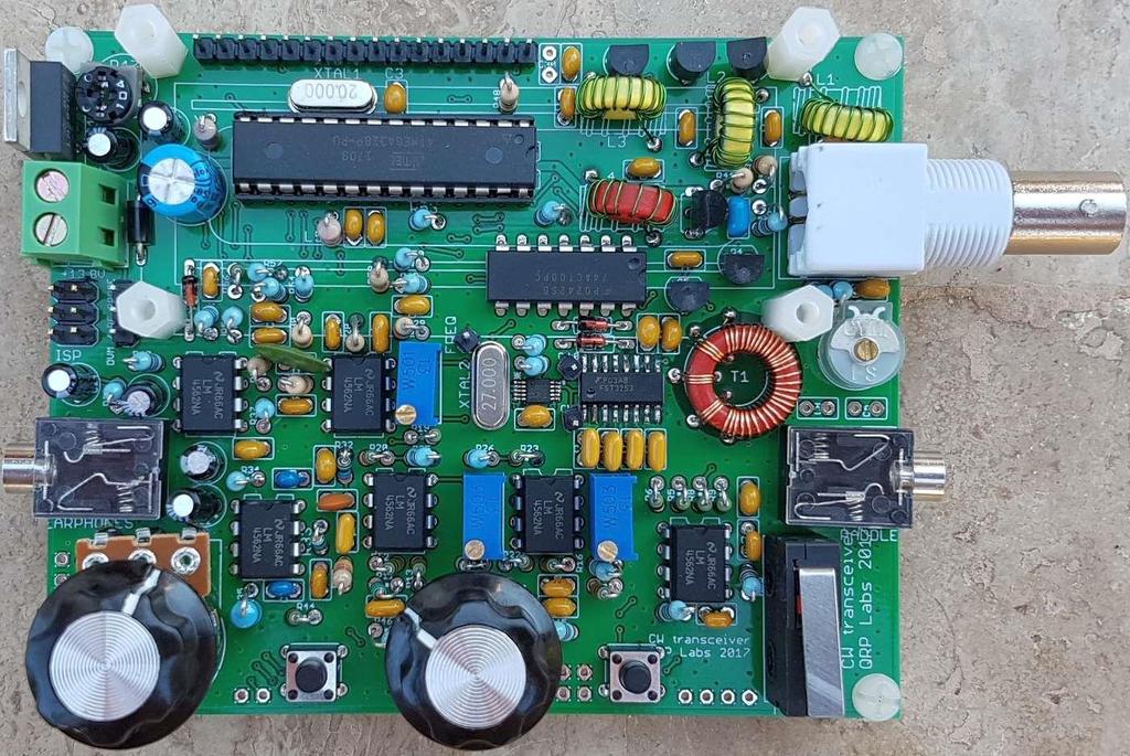
9 3.1 Inventory parts Refer to parts list in section 2. The following photographs are to aid component identification. The resistors and capacitors are omitted. Rev

10 3.2 Install IC2 socket Install the 28-pin IC socket for IC2. Take care to match the dimple on the socket, with the dimple on the PCB silkscreen. It is critical to insert the microcontroller with the correct orientation. Lining up the dimple on the PCB silkscreen, socket and actual IC is the best way to avoid confusion and potential error. I recommend soldering one pin at each diagonal, for example pins 1 and 15. You can then check that the IC socket is seated firmly on the PCB, and correct any issues easily. Once all the pins are soldered it will be difficult, if not impossible, to change anything. When you are happy with the position of the socket, proceed with soldering the other 26 pins. 3.3 Install DIP integrated circuits IC3, IC5-10 In the same way, install the Dual-Inline-Package integrated circuits IC3 and IC5-10. We install these now because they have more pins than all the passive components (resistors, capacitors etc) and it is easiest to reach and install the ICs properly when they are alone on the board. All of the operational amplifier ICs (IC5-IC10) are part number LM4562, so it is impossible to mix them up, they are the only 8-pin DIP chips in the kit. Similarly, IC3 is the only 14-pin DIP chip. Electrostatic Discharge (ESD) precautions should be observed though personally I do not think it is necessary to get crazily paranoid about this. Don t wear 100% nylon clothing and dance around on a nylon carpet etc to build up static charge! But I don t go to the other extreme of earth mats, earthed wrist bands etc. Rev
11 It IS absolutely critical to align the IC s properly! Be very careful to check and double-check and even triple-check that the dimple in each IC package is aligned with the dimple in the silkscreen print on the PCB (and the layout diagram). As before, I find it useful to solder initially two pins at diagonal opposites of the chip, then check that the chip is nicely seated evenly on the board, before soldering the other pins. 3.4 Install all 100nF (0.1uF) capacitors There are nF (0.1uF) capacitors, these have the code 104 written on them. Be sure to identify the correct capacitors, using a magnifying glass or jeweller s loupe. These capacitors are C2, C3, C6, C12, C29, C32, C34, C35, C36, C39, C40, C41, C48, C49, C50 and C52. Place each in the correct position on the board, and slightly bend outwards the legs at about 30-degrees angle so that they stay in place. Then solder the wires, and trim the excess wire length with wire cutters. It does not matter which way round the capacitors are installed. However, it is very good practice to install them all with the capacitor label facing in the same direction. For example, ensure all the 104 labels face to the front, or to the right (depending which way the capacitor is orientated on the PCB). This makes it much easier to inspect the PCB assembly later. Rev
12 3.5 Install all 470nF capacitors The 470nF capacitors are labelled 474, and are capacitors C11, C43, C44, C45 and C46. Rev
13 3.6 Install all 1nF capacitors The 1nF capacitors are labelled 102 and are capacitors C14, C16, C18, C23 and C Install all 10nF capacitors The 10nF capacitors are labelled 103 and are capacitors C4, C7, C10 and C42. Rev
14 3.8 Install 47nF capacitors The 47nF capacitors are labelled 473 and are capacitors C9 and C Install 39nF capacitor The 39nF capacitor is labelled 393 and is C17 (or it may be supplied as 40nF, label 403 ). Rev
15 3.10 Install 2.2nF capacitors The 2.2nF capacitors are labelled 222 and are C19 and C Install 33nF and 3.3nF capacitors These are labelled 333 and 332, and in parallel make up 36nF. They are C15 and C53. Rev
16 3.12 Install capacitors C25 and C26 from the Low Pass Filter kit These are labelled 271 and have value 270pF Install capacitors C27 and C28 from the Low Pass Filter kit These are labelled 101 and have value 100pF. Rev
17 3.14 Install capacitor C30 This capacitor is band dependent. For 17m it is 30pF. The code written on this capacitor is IGNORE C5 and C8 C5 and C8 are not installed in the 17m version of the kit. So ignore this step. Rev


18 3.16 Install 1uF capacitor The 1uF capacitor is labelled 105 and is C Install 1N4148 diodes There are 4 small glass red-ish coloured diodes, D1, D2, D4 and D5. Note that D1, D2 and D5 are installed flat on the PCB (see photo, right). D4 is installed vertically, (see photo, far right). In all cases it is critical to install the diodes the right way around, these are a polarised component and must only be installed in the PCB with the correct orientation! In the case of D1, D2 and D5, the PCB silkscreen printing shows a white stripe at the end of the diode body which must match the black stripe on the left end of the diode (photo above). For D4, the black strip on the diode body must be orientated with the horizontal bar of the diode symbol on the layout diagram (see photo, right). D4 is mounted vertically. The location of D4 is indicated by the red square, near the top right of the diagram on the following page. Rev
19 3.18 Install 1N5819 diode This diode D3 is the larger diode with a black body, and a white strip. It is installed horizontally. Again, it must be orientated correctly, with the white stripe on the diode matching the white stripe on the PCB. This diode protects the radio against reverse polarity. So that if you connect the power to the board the wrong way around, you do not destroy it. A Schottky diode is used because the forward conducting voltage drop is less than an ordinary diode. However, on transmit, the voltage drop across this diode can still be up to 400mV. This reduction in voltage does slightly decrease the output power. IF you want to squeeze every last milliwatt of output power out of the radio, and IF you trust yourself NEVER to connect the power supply in reverse by mistake, then if you just install a jumper wire instead of D3, it would give you a little higher RF power output. Rev
20 3.19 Install 20MHz crystal XTAL1 The engraving on this crystal is Rev

21 3.20 Install 27MHz crystal XTAL2 The engraving on this crystal is Install all 10K resistors There are 15 10K resistors in the kit, these are R1, R2, R7, R10, R14, R34, R39, R40, R46, R49, R50, R51, R52, R57 and R58. The colour code is brown-black-black-redbrown. All of the resistors in the kit are installed vertically (see photo, right). Resistors are not polarised components and it does not matter which way around they are installed. For simplicity I recommend installing the body end of the resistor next to the circle on the PCB silkscreen (and the layout diagrams). Rev
22 3.22 Install all 1K resistors There are 12 1K resistors in the kit, these are R3, R4, R25, R26, R37, R42, R45, R53, R54, R55, R62 and R63. The colour code is brown-black-black-brown-brown. Rev
23 3.23 Install all 3.3K resistors There are K resistors in the kit, these are R12, R13, R15, R16, R19, R20, R22, R23, R44, R56 and R59. The colour code is orange-orange-black-brown-brown Install all 100-ohm resistors There are four 100-ohm resistors in the kit, these are R5, R6, R8 and R9. The colour code is brown-black-black-black-brown. Rev
24 3.25 Install 120K resistors There are three 120K resistors in the kit, these are R38, R43 and R60. The colour code is brownred-black-orange-brown Install 33K resistors There are two 33K resistors in the kit, these are R28 and R29. The colour code is orange-orangeblack-red-brown. Rev
25 3.27 Install 47K resistors There are two 47K resistors in the kit, these are R30 and R31. The colour code is yellow-purpleblack-red-brown Install 36K resistors There are two 36K resistors in the kit, these are R32 and R33. The colour code is orange-blueblack-red-brown. Rev
26 3.29 Install 270-ohm resistor R48 This resistor has colour code red-purple-black-black-brown Install 470-ohm resistor R41 This resistor has colour code yellow-purple-black-black-brown. Rev

27 3.31 Install 3.9K resistor R61 This resistor has colour code orange-white-black-brown-brown Install 4.3K resistor R18 This resistor has colour code yellow-orange-black-brown-brown. Rev
28 3.33 Install 5.1K resistor R11 This resistor has colour code green-brown-black-brown-brown Install 7.5K resistor R21 This resistor has colour code purple-green-black-brown-brown. Rev
29 3.35 Install 750K resistor R35 This resistor has colour code purple-green-black-orange-brown Install 100K trimmer potentiometer R47 This is the LCD contrast potentiometer. The label on R47 is 104. Carefully apply firm pressure to install the component pins in the holes without bending them. Rev
30 3.37 Install 500-ohm multi-turn trimmer potentiometer This resistor is the small blue box component with label 501. It is R27. Make sure that the orientation is correct. The screw on the resistor should match the screw on the PCB silkscreen and layout diagram Install 50K multi-turn trimmer potentiomers There are two 50K multi-turn trimmer potentiometers, R17 and R24. They are the small blue box components with label 503. Make sure that the orientations are correct. The screws on the resistor should match the screws on the PCB silkscreen and layout diagram. Rev
31 3.39 Install two 100uH inductors There are two 100uH inductors, L5 and L6. These look like short fat resistors. They are installed vertically on the PCB, in the same way as the resistors are installed. Rev
32 3.40 Install 10uF capacitors There are six 10uF capacitors in the kit: C21, C22, C24, C37, C38 and C51. These are polarised electrolytic capacitors and MUST be installed with the correct orientation! The capacitor NEGATIVE wire must be installed in the hole indicated on the PCB silkscreen and the layout diagram by the solid black bar; the POSITIVE wire must be installed in the hole indicated on the PCB silkscreen and the layout diagram by the hollow bar and the + symbol. Electrolytic capacitors are also supplied with one wire longer than the other. The + wire is the longer wire, the wire is the shorter one (see photo, right) Install 220uF capacitor C47 (may be supplied as 470uF) This capacitor is also a polarised electrolytic and must be orientated correctly (see former section). Rev
33 3.42 Install 30pF trimmer capacitor C1 Insert the component pins carefully and solder them QUICKLY to avoid overheating the capacitor which could melt the plastic insulating spacers. Rev
34 3.43 Install MPS2907 transistor Q6 Be careful to correctly identify this transistor by its markings, as the package style is similar to the other transistors. Carefully bend and insert the wires so that the transistor orientation matches the PCB silkscreen and the layout diagram. Carefully push the transistor down towards the PCB until the wires between the PCB and the transistor body are about 5mm long, then solder Install all BS170 transistors The remaining transistors in the kit are BS170 MOSFETs and there are six of them: Q1, Q2, Q3, Q4, Q5 and Q7. Follow the same installation procedure as the previous section. Rev
35 3.45 Install 2x3-pin in-circuit programming header This pin header can be used to connect an AVR Programmer to apply firmware updates if desired. Solder one pin in place first and check that the header is nicely seated on the PCB before soldering the other 5. Rev
36 3.46 Install 4-pin GPS header Install a 4-pin header from the Low Pass Filter kit, in the position shown. This is used to connect a GPS module if required Install 3-pin DVM/RF detector header Take the other 4-pin header from the Low Pass Filter kit and carefully cut off 1 pin with a wirecutter, without damaging its plastic base. The headers are designed to break apart easily like this. Keep the 1-pin section safely. Install the 3-pin header section as shown. This is used as the input to the DVM (voltmeter) and RF power meter functions of the kit. You can later jumper pins 1 to 3 to measure the supply voltage with an icon on the LCD during operation. Rev
37 3.48 Install 1-pin test points Install 1-pin headers as test points, as shown. One of these is taken from the 4-pin header from the Low Pass Filter kit (see previous section); the other two are to be cut carefully from the 16-pin header supplied, leaving the 14-pin section intact. Rev
38 3.49 Install power connector Install the 2-way power connector as shown, orientated to match the PCB silkscreen and have the terminal openings facing outwards from the PCB to facilitate installing power wires later Install 7805 voltage regulator IC11 Install the 7805 voltage regulator, orientating it so that the metal tab is facing outwards from the PCB. Push the wires all the way down into the holes until the body of the regulator is about 5mm off the PCB surface. Solder and trim the excess wires under the board. Rev
39 3.51 Install pin headers for the LCD module The LCD has a 16-way connector. If you have been following me so far, You have already carefully cut off two of the pins, to use in the Clk0 and Clk1 test points. Therefore you only have a 14-pin header remaining. This is fine, since not all of the pins of the LCD module are used! The LCD module has an 8-bit data bus, but can also be operated in 4-bit data mode, which is what is done in this kit. The 4-bit mode has the advantage that less pins of the microcontroller are used! This is very important in this design, because we require so many control pins from the microcontroller for the various functions of the radio. So the LCD has 16 pins but the central 4 pins are not used. Now break the 14-pin header carefully in half so that you have two 7-pin sections. (If you make a mistake and you have one 8-pin section and one 6-pin section, that is still Ok). Install the two sections into the 16-pin holes on the PCB leaving an empty gap of two pins in the middle. Be very careful to ensure that the pin headers are accurately aligned to the PCB, so that later when we install the LCD module everything fits accurately. Rev
.")
40 3.52 Wind and install toroid L4 L4 is type T37-2. It is a small ring with red paint on one side. For 17m band, wind 9 turns of wire onto this toroid. Each time the wire passes through the hole in the middle of the toroid, this counts as one turn. Try to keep the wire quite tight (but not so tight that you break the wire). Try to spread the turns evenly around the toroid. Leave about 2cm of wire at the ends. The wire is coated with an enamel insulating paint and it is CRITICAL to remove this enamel at the soldered joints otherwise there will be no electrical connection through the toroid! This is the number 1 cause of problems with QRP Labs kit construction: failure to remove the wire enamel. One method of removing the wire enamel is to scrape it off at the ends, either with sandpaper, or carefully scratching with a knife or wire cutters. However, my favourite method is just to burn off the enamel. For quite a number of years, the type of enamel used on copper wire can be burnt off using the temperature available from an ordinary soldering iron, immersing the wire in a blob of solder. (This was not the case, with much older wire found in vintage valve/tube equipment). You could also use a cigarette lighter to burn off the enamel. Insert the ends of the wires into the correct holes of the PCB and pull it through tight, so that the toroid sits up vertically on the PCB. See photo, right. Bend the wires over so that the toroid does not fall out while you are trying to solder the wires. Cut off the excess wire using wirecutters, leaving only about 2mm protruding through the PCB on the lower side. Now apply solder quite generously from the soldering iron. Hold the soldering iron to the joint for a few seconds I usually count to 10 slowly) and the solder will surround the wire, which will become hot enough to burn off the enamel. You can sometimes see a small puff of smoke when the enamel burns off. Carefully inspect the soldered joints with a magnifying glass to make sure that the wire is correctly soldered. If it looks like the solder hasn t flowed nicely and adhered to the wire, then this is usually a sign that the enamel probably hasn t been burnt off. If you have a DVM it is a good idea to check for DC electrical continuity (zero ohms resistance) between the two ends of the wire. If you do NOT have a DVM and if the radio doesn t work, then we can use the built-in test equipment later, to trace the fault. Rev
41 3.53 Wind and install toroid L2 In the 17m kit, L2 is a small toroid ring painted yellow on one side. It is part of the 17m Low Pass Filter kit. For the 17m kit, wind 15 turns onto the toroid, again keeping the wire tight and evenly spaced around the toroid. Installation of the inductor is similar to the previous section. Rev

42 3.54 Wind and install toroids L1 and L3 In the 17m kit, L1 and L3 are a small toroid ring painted yellow on one side. They are part of the 17m Low Pass Filter kit. For the 17m kit, wind 13 turns onto each toroid, again keeping the wire tight and evenly spaced around the toroid. Installation of the inductors is similar to the previous section Wind and install transformer T1 Now we come to the only really tricky piece of the assembly, which is the receiver input transformer T1. Follow these instructions carefully, it is tricky but quite feasible if the you go step by step. In the end, you are going to end up with an installed transformer which hopefully looks something like the photo (right). This transformer has FOUR windings. Three identical short windings, and one long winding. There are therefore eight wire ends, which must all be soldered into the correct holes on the PCB, and with the enamel properly removed. Rev
43 Here are two diagrams which numerate each of the windings, wire endings and holes on the PCB, on both the layout diagram and on the circuit (schematic) diagram. It should help to explain diagrammatically which wires must go where. The four windings on T1 must all be in the same sense. There are two ways to wind toroids. You might call them left-handed and right-handed; clockwise and counter-clockwise; whether the wire goes through the toroid hold from top to bottom, or from bottom to top. Whatever you call it, all the four windings have to be the same, to be sure to get the phasing to the quadrature sampling detector correct. For the 17m transceiver kit, the three short windings have 3 turns, and the long winding has 30. To make things easier, we will wind all 39 windings together in one go, this will guarantee that the Rev


 When you have completed 30 turns, pass the wire through the hole for the 31st turn but leave a large loop of wire between")
 Grip the toroid and wound turns tightly between thumb and finger, and with the other hand apply some twists the wire")
44 sense of each winding will be the same. At the intended breaks between the windings, we will leave large loops of wire, that we can later cut one by one to make sure the wires go in the correct holes. There are a lot of steps listed below, but in reality it is easier DOING it than it is writing instructions how to do it. Step by step: 1) Hold the toroid between thumb and finger, and thread the first turn of the wire through from top to bottom. Leave about 3cm of wire at the free end. 2) Apply tension to the wire after each pass through the centre hole, to try to keep the windings tight and even. The wire turns should sit neatly side-by-side on the toroid, without overlapping. 3) Grip the toroid between thumb and finger as you wind. 4) When you have completed 30 turns, pass the wire through the hole for the 31st turn but leave a large loop of wire between the 30th and 31st, without pulling it tight. 5) Grip the toroid and wound turns tightly between thumb and finger, and with the other hand apply some twists the wire loop, tight next to the toroid. 6) The result is a wire loop after 30 turns, as shown. 7) Do the same thing for two more loops, which are between the 33 rd and 34 th turns, and 36 th and 37 th turns respectively. It is easy to lose count. An easy way is after step 6, pass the wire through the hole 3 more times, and on the 3 rd one, make a loop. Similarly count three more and make a loop on the third. Then finally three more turns to complete the Rev
 The remaining steps show the transformer installation on an otherwise empty PCB, to make the explanation clear.")
 Twist these two wires under the board to keep the toroid in place while you deal with the remaining wires.")


 Similar to step 11; the wire which came over the toroid body has three turns then goes into hole 4, which you did in step 11. Insert this wire-end into hole 3.")
45 toroid s 39 windings. Count the windings to make sure you have 39. When you are sure everything is fine, cut the wire leaving about 3cm of wire free at the end. 8) The remaining steps show the transformer installation on an otherwise empty PCB, to make the explanation clear. Thread the original start of your winding (from step 1) into hole 1 in the diagram. Thread the final end of your winding (from step 7) into hole 6. 9) Twist these two wires under the board to keep the toroid in place while you deal with the remaining wires. 10) Now cut the 3 rd loop (the one nearest the end of the winding work), and un-twist the twisted section you made near the toroid body. 11) When you cut the loop, you therefore created two wires. One of these came over the top of the toroid, and you can easily verify that this is the one which has three turns through the toroid then passes through hole 6. So insert this wire into hole 5. Once again to be clear: you should now have a winding of three turns (which is labelled secondary 2, above), with one end inserted into hole 6 and one end inserted into hole 5. The other wire, came from UNDER the toroid. You must push this wire towards the toroid and pull it out through the centre hole of the toroid. Now thread it through hole 4. Under the board, twist the two new ends of wire together to keep them in place. 12) Next cut the 2 nd loop, and un-twist the twisted section near the toroid body. 13) Similar to step 11; the wire which came over the toroid body has three turns then goes into hole 4, which you did in step 11. Insert this wire-end into hole 3. The other wire end that came from under the toroid body should be gently pushed toward the toroid, and pulled up through the centre hole of the toroid. Insert that wire end into hole 8. So now you have the primary winding consisting of three turns, between holes 3 and 4. Twist the two new wires under the board again, to keep everything in place. Rev


 Under the PCB, you should have three pairs of twisted wires, and one pair (that you installed last), un-twisted. 17) Now you can solder the eight connections under the PCB.")

 across each winding.")
46 14) Finally, cut and un-twist the loop which you created first, which was between the 30 th and 31 st turns of the toroid winding. Push the wire which came over the toroid body, into hole 7. Now you have three turns of wire, which make up secondary 2, between holes 7 and 8. 15) The last wire came from under the toroid body when you cut the loop; this wire is the other end of the 30 turns secondary 3 winding, so insert it into hole 2. It is already near to hole 2 and you don t need to push it under the toroid body as you did in previous steps. Take a moment now to review the situation. You should be able to identify the four windings of T1, and squeeze them together neatly as in the photo, to verify that each end of the 3-turn windings goes into the correct holes. 16) Under the PCB, you should have three pairs of twisted wires, and one pair (that you installed last), un-twisted. 17) Now you can solder the eight connections under the PCB. I recommend doing one pair of wires at a time; this way, the other wires will hold the toroid in place and stop it falling out. Start with the two un-twisted wires. Pull each wire tight, bend it over at about 45-degrees, and cut it 1-2mm away from the PCB surface. Having bent the wire prevents it from falling out. Now solder the wire. Remember to hold the soldering iron to the joint for 10 seconds or so, to allow the enamel insulation to burn off. Repeat for all the other wires, one pair at a time, until all eight are soldered. If you have a DVM, check for DC continuity (zero ohms resistance) across each winding. If you do not get the expected continuity, then it means either a) you have not managed to scrape or burn away the enamel insulation properly so there is no electrical connection AND/OR b) you put the wires into incorrect holes AND/OR c) your expectation is wrong because you have not identified which pad on the PCB is labelled 1-8 in the diagram. Rev


47 18) The final picture (18) shows the toroid installation completed Install RF output BNC connector Solder one pin first, to check that the alignment is correct; when happy, solder the remaining pins. The connector has RF and Ground connections, and two fat rods which are for mechanical stability only. Rev
48 Install 3.5mm stereo connectors These connectors are used for the audio output (earphones) and for optional connection of a paddle. In each case, solder two opposite pins first, holding the socket in alignment. When you are happy that the socket is neatly aligned and seated on the PCB, solder the remaining pins Install buttons S2 and S3 (left and right buttons) These buttons (or other push-to-make buttons) may alternatively be wired off-board, for example when mounted in a front panel. Refer to later section for wiring details. Rev
49 3.58 Install rotary encoder This switch has seven solder pads: five are for electrical connections and the two large tabs are for mechanical stability. You may also choose to mount the switch off-board, for example on a front panel. Refer to the later section describing the wiring. Remember that it will be difficult to remove the switch later, so you may wish to make the external mounting decision now Install microswitch The microswitch can be used as an on-board straight key if desired and is suprisingly effective! The PCB holes are large so be sure to use enough solder to make good joints. Rev

50 3.60 Install gain control potentiometer R36 Carefully bend the pins of the potentiometer upwards 90-degrees as shown in the photograph. Remove the nut from the potentiometer, fit the shaft through the hole in the PCB, and carefully install the bolt and tighten with pliers. There is an anti-rotation tab on the metal case, which fits in the smaller hole to the right of the main shaft hole. The tab hole is near to C52, on the right of the potentiometer. When tightening the nut ensure that the pins remain aligned with the corresponding pads on the PCB. Be very careful with this potentiometer and do not over-tighten the nut. The potentiometer is quite delicate. The three pins do not extend far enough to fit into the three corresponding holes on the PCB. However they are close enough that a generous blob of solder is enough to make a reliable connection to each pin Install four 12mm hex spacers at the LCD corners Install the four 12mm spacers on the top side of the PCB, threading four M3 nylon screws through from the underside of the PCB. These four spacers fix the LCD module to the PCB assembly. Rev
51 3.62 Install four 12mm hex spacers at the PCB corners These spacers are installed on the bottom side of the PCB, with the four M3 screws threaded through from the top (component) side. These four spacers make four little pillars at the board corners, to keep the underside suspended above your workbench or fixing to an enclosure. Rev

52 3.63 Install knobs Two black knobs are supplied, one for the rotary encoder and one for the gain control. When fitting the gain control knob, you should ensure that when the potentiometer is turned all the way anticlockwise, the white pointer on the knob points to the bottom left corner of the PCB. This is the conventional alignment for volume control knobs Install 16-pin female connector on LCD module The 16-pin female header connector must be installed on the solder-side of the LCD module, so that it will mate with the 16-pin male header on the main transceiver PCB. The easiest way to do this is to temporarily assemble the modules and bolt the LCD in place using the supplied nylon M3-sized screws. The nylon headers at the LCD module corners are a little longer than would be ideal. Accordingly leave a small gap between the 16-pin female header connector, and the LCD module itself. Push the female header connector all the way onto the 16-pin header on the main PCB, and solder the pins in place Install microcontroller Finally install IC2, the programmed ATmega328P microcontroller. Be very careful to ensure that the dimple on the chip is aligned with the dimple on the 28-pin DIP socket, which itself should already be aligned with the dimple on the PCB silkscreen Install LCD and the remaining 4 screws to bolt LCD module Now plug in the LCD module and screw it in place, using the remaining 4 nylon M3 screws. Rev
53 3.67 Connections for off-board mounting of controls The following wiring diagram shows the connections between the PCB pads and controls (buttons, rotary encoder, gain potentiometer) that should be made if you intend to wire the controls offboard. For example, you may wish to install the radio in an enclosure and mount the controls on a front-panel. The diagram shows the two buttons, gain potentiometer and the rotary encoder. PCB pads are also available for the microswitch Morse key as labelled in black (bottom right) but typically you would probably wish to plug a key or paddle in to the 3.5mm socket. If installing the radio in an enclosure you would also want to wire the LCD module to the PCB rather than plug it in directly. Take care to ensure short cables, or use shielded (screened) cable in order to avoid radiating digital noise into the RF circuits. Rev
.")
54 3.68 Connections for basic operation The following diagram illustrates the basic connections for transceiver operation. A power supply is required, which needs to be able to supply up to 0.5A on transmit. The supply voltage may be from 7 to 16V, and the RF power output will depend on the supply voltage (power output power is produced at higher supply voltages). Note that the 7805 voltage regulator requires no heatsink; however the heat production will increase as supply voltage is increased, and the IC does get uncomfortably hot to touch at 16V supply. Although I still not believe it is necessary, you may feel less disturbed if you fit a small heatsink to the 7805 voltage regulator if you intend to operate at higher supply voltages. The earphones can be any stereo earphones such as commonly used with audio equipment, mobile phones and so on. The RF output is a filtered 50-ohm output for connection to a usual antenna system (antenna, and matching unit if applicable). Rev

55 3.69 Adjustment and alignment The first thing that you will notice when you apply power to the radio, is that there is probably nothing at all shown on the display. This is because you need to adjust the contrast trimmer potentiometer R47 at the top right of the PCB! Adjust it with a screwdriver until the display text looks right to you. There are four more adjustments which now need to be made as part of the alignment procedure. The adjustments are: Band-pass trimmer capacitor peaking, C1 I-Q amplitude balance, R27 Audio phase shift adjustments, R17 and R24 Until these are adjusted, the sensitivity of the radio will be very low. So do this first, before going any further! The location of these five adjustments is indicated on the following diagram. In summary: the alignment tools built into the radio consist of a signal generator which injects a signal into the RF front end, and digital signal processing which adds a 250-Hz digital filter to the existing 200Hz analogue filter, and calculates the amplitude of the signal detected in that bandwidth. During alignment, the amplitude is displayed on-screen as an intuitive bar across the bottom row of the display. Using a screwdriver, you adjust the trimmer component in order to maximise or minimise the displayed amplitude. Unplug the antenna during alignment of the radio! Rev
 button, to enter the alignment menu.")
56 First adjust the band-pass trimmer capacitor C1. To do this, give one long press to the left button. The screen now displays the first menu category: 1 Preset Turn the rotary encoder until you see the alignment menu: 8 Alignment Now press the left ( select ) button, to enter the alignment menu. For 17m operation, the alignment frequency menu item should be set to a frequency in the CW section of 17m, as follows: 8.1 Align frq 18,120,020 If you do not see 18,120,020 here, then you need to adjust the frequency to 18,120,020. To adjust the frequency, click the left ( select ) button and a cursor appears under the left-most digit. Use the rotary encoder to adjust the digit value, then press select again to move right 1 character to the next digit. When you have changed the displayed value to show 18,120,020 press the right ( exit ) button to save the edited value; the cursor underline now disappears. Now turn the rotary encoder until you see: 8.7 Peak BPF Press Select! Do as it says! But if you have earphones plugged in, please take them out of your ears first. Press the left ( select ) button to switch on the signal generator so you can adjust the C1 trimmer potentiometer. Now if you have earphones plugged in, you will hear a loud tone at 700Hz. The display will look like this photograph: Adjustment of the C1 trimmer capacitor should change the size of the amplitude bar. You need to adjust the C1 trimmer for MAXIMUM amplitude. When this is done, the peak of the band pass filter will be centred on the CW section of the band. Rev
57 It is very important to understand the number at the top right of the LCD, here shown as 09. This is an amplitude scaling factor, expressed as a power of 2. In this example, the actual amplitude is divided by a factor of 512 (2 to the power of 9) then displayed on the screen. In this photograph, 27 little vertical bars are shown, which means the actual measured amplitude value is 13,824. If the displayed bar drops below one third of the width of the LCD, then the division factor is reduced by one and the bar is re-displayed. On the other hand, if the displayed bar overflows the right edge of the screen, the division factor is increased by one. This simple method creates an auto-scaling display of the amplitude. Therefore, to peak the band pass filter trimmer, first adjust the trimmer potentiometer while looking at the division factor in the top right of the LCD. Then carry out the fine adjustment using the displayed amplitude bar. The peak is quite sharp. Be wary because there can be more than one peak (more than one response of this simple band pass filter). So, tune the trimmer capacitor through its whole range, and determine the maximum scaling factor that you see. In my case here, it is 09. Then make the very fine adjustment necessary to peak the amplitude bar. Now turn the rotary encoder one click clockwise. Note that the previous alignment used the audio signal BEFORE the final amplification stage, so the gain control had no effect on the signal level. In contrast, the I-Q balance and audio phase shift adjustments use the audio signal AFTER the audio amplification stage. This is necessary because these alignment adjustments inject a signal into the opposite (unwanted) sideband, and the signal level is much lower, therefore it needs to be amplified for the microcontroller to be able to measure it accurately. In this case therefore, the gain control does now have an effect. I suggest adjusting the gain control approximately to mid-way. This will provide enough gain, yet not so much gain that the amplifiers are driven into overload, which distorts the signal and measurements. The I-Q trimmer potentiometer is R27. It is a multi-turn trimmer potentiometer so it may need to be turned quite a few times to get to the optimum value! For this adjustment, you are looking for the MINIMUM amplitude, not the maximum we adjusted the BPF trimmer to. We adjust for minimum because now the injected signal is measuring the unwanted sideband. We want to MINIMISE the unwanted sideband level. Similarly turn the rotary encoder one more click clockwise, which automatically sets the unwanted sideband audio signal to appear at 600Hz, and adjust the low audio phase shift trimmer potentiometer, R24. Again, adjust it for MINIMUM signal. Turn the rotary encoder clockwise one more click and adjust the high audio phase shift trimmer potentiometer R17, again for minimum signal. Now it is necessary to go back and forth between these three menu items for minimum unwanted sideband: 8.8 I-Q Bal (adjust R27) 8.9 Phase Lo (adjust R24) 8.10 Phase Hi (adjust R17) This is because to some extent, these adjustments influence each other. Obtaining the optimum set of adjustments is an iterative process. So, turn the rotary encoder a click at a time anticlockwise or clockwise, back and forth through these three menu items. Each time make small further adjustments to the appropriate trimmer potentiometer and observe the lower amplitude. Keep doing this until you see that you cannot really manage to get the unwanted sideband any Rev
58 lower. Pressing the right (exit) button twice leaves the menu system and returns the radio to normal operation. Other items in the alignment menu relate to the calibration of the 27MHz reference oscillator of the synthesiser, and the 20MHz system clock oscillator of the microcontroller. These adjustments can be made manually, or by connection of a GPS module such as the QRP Labs QLG1 GPS receiver kit. However, since this calibration is a lot less urgent than the Band Pass Filter peaking and unwanted sideband cancellation, they are left until the description of these menu items in the operating manual. Following the adjustment of these alignment trimmers, the radio is ready to use. A lot of settings are available in the configuration menu, and you should read the operation manual to understand and make use of all the features! 4. Operating instructions 4.1 Overview of features This 5W CW transceiver kit includes a large number of features defined by the firmware in the ATmega328P microcontroller chip. The following is a brief summary of the features to explore and enjoy. Read the subsequent sections for more detailed information on these features. Synthesised VFO with rotary encoder tuning The VFO is an Si5351A Synthesiser chip, configured by the microcontroller. An rotary encoder tunes the VFO, with a variable tuning rate. The radio includes two VFOs, A and B. You can swap from one to the other, copy the contents of the active VFO to the inactive one, or operate Split (Transmit on VFO A, receive on VFO B). There is also a RIT mode offering a receive offset of up to +/- 9,999Hz. The CW offset is also adjustable, and CW-R (sideband swap) mode is supported. Memory features There are 16 frequency presets for your favourite operating frequencies. Each frequency preset can be edited in the configuration menu, or loaded/saved into/from the currently operating VFO. Message mode The firmware supports storage of 12 messages. Four of these are 100 characters long, the other eight are 50 characters long. A single button click shows the list of messages to send. Message sending can be configured to send just once, or a configurable number of times, or indefinitely repeating. The interval between transmissions is also configurable. The message feature can be useful, for example, for setting up a repeated CQ call with a pause between repeats, during which you can listen for any answers. As soon as you touch the key to begin transmitting, the automatic message mode is cancelled. CW Keyer There is an onboard microswitch which can be operated as a straight (traditional) Morse key. The firmware also includes an Iambic keyer, for connection of a paddle. The keyer can be configured to operate in Iambic modes A or B, or Ultimatic mode. The keyer speed is variable both from the configuration menu and via a single button press during operation. Rev
59 With its solid-state, microcontroller operated transmit/receive switch, the radio can operate in full break-in QSK mode, or if you prefer, semi-break in. CW Decoder A CW decoder operates in the chip. This can be useful on air, particularly for newcomers to CW, though it is never anywhere near as good in QRM or weak signal conditions as a good CW operator using the wet-wear between his ears. The decoder has a Practice mode too, for you to practice your CW sending without actually generating RF. The decoder can also be used to conveniently enter text in the message storage, or for configuration of any of the other menu items. The decoder can also be switched off if desired. CW or WSPR Beacon mode A beacon is included too, and this can be configured to operate in CW mode or WSPR mode. Owners of the QRP Labs Ultimate-series weak signal mode transmitter kits will be familiar with the operation of WSPR. A GPS module such as the QRP Labs QLG1 GPS receiver kit can optionally be connected to this CW transceiver kit to provide frequency and time discipline, as well as setting the Maidenhead locator (from latitude and longitude) that is encoded in the WSPR message. S-meter and Battery voltage An S-meter and battery voltage indicator can be enabled for display on the LCD. These are both configurable to your needs. The battery voltage indicator would be useful if you intend to operate the radio portable on battery power. Built-in alignment tools One of the nicest features of this CW transceiver kit, is the built-in alignment tools menu. The radio can act as its own signal generator, injecting an appropriate signal into the receiver front end, then measuring the audio amplitude after single-sideband demodulation. The menu items allow you to easily peak the Band Pass Filter adjustment, and to adjust the I-Q balance and audio phase shift adjustments for best unwanted sideband cancellation. Built-in test equipment For those times when the assembly didn t quite go as well as we hoped, and we need to do some debugging the radio includes its own suite of test equipment too! None of these items of test equipment are going to replace a $100,000 lab any time soon but they provide very useful measurements for helping people without much test equipment, to debug the radio. They can even be used for testing other projects too! Voltage meter RF Power meter Audio channel amplitude measurements Frequency counter (0 to 8MHz) Signal generator (3.5kHz to 200MHz) Rev
 is shown in the above photograph.")
60 4.2 Display elements The kit uses a 2 row, 16 character LCD module with a blue backlight. The main display layout during ordinary operation (which will be called main operating mode ) is shown in the above photograph. The display during beacon or message transmission modes, menu editing, alignment etc. differs. The main display elements are as follows: The transmit VFO frequency is always displayed, to 10Hz resolution, at the top left. This may be VFO A or VFO B. Ordinarily this frequency is also used for reception (apart from the automatically applied 700Hz CW offset). Tuning rate cursor: the underline appears under the digit which is currently tuned by the rotary encoder. In this example, the tuning rate is 100Hz per click, because the cursor is under the 100Hz digit. S-meter: these 4 characters display a basic (and not calibrated) S-meter. The scale is configurable (see later description). The S-meter may be shown or hidden. Battery voltage: a battery icon appears to indicate the battery voltage in 7 user-definable steps: from full to empty and 5 steps in between. It may also be shown or hidden. Receive VFO: in SPLIT mode, the receive VFO is displayed on the bottom row of the display. RIT (Receiver Incremental Tuning): when not in SPLIT mode, and when the RIT is nonzero, the RIT value is displayed in the bottom left (where the photo shows the VFO B frequency). When RIT is non-zero, and when not in SPLIT mode, the reception frequency is the transmit VFO frequency (which may be VFO A or B) plus the RIT (which may be a negative offset). Decoded CW: The remaining space on the bottom row is used for displaying the decoded CW text. When RIT is zero, and you are not operating SPLIT, the whole 16 characters of the bottom row are used for the CW decoder display. However, it may be hidden if desired. Rev
61 4.3 Operator controls This diagram shows the operating controls of the radio. All of the controls except the Gain potentiometer have multiple functions, depending on the operating mode, menu editing, etc. The tuning rotary encoder in the centre has a button on its shaft that is activated by pressing it, and this button also has multiple functions. In this document, the three buttons are mostly referred to as Left, Centre and Right. The original names of the left and right buttons, Select and Exit respectively, refer to the common actions during configuration menu editing. Select edits a menu item or steps down into a submenu; Exit saves an edited menu item or backs up to the parent menu. It is well worth remembering while you are familiarising yourself with the operation of the radio, that if you get into any unexpected function or menu you can nearly always press the right (exit) button to cancel and get back to the main operation mode. Each of the buttons (left, centre, right) may be pressed once, pressed twice (a double-click) or pressed for a long-hold. This facilitates three different functions for each button. In practice the centre button is stiffer and it is difficult to achieve a double-click; therefore the centre button double-click has no function. 4.4 Tune rate The rotary encoder tunes the active VFO. The rate of tuning is indicated by the underline cursor. In the example below, the underline cursor is under the comma between the 1kHz and 100Hz digits. This means the tuning rate is 500Hz. The available VFO tuning rates are 1kHz, 500Hz, 100Hz or 10Hz. A press of the centre button (in the rotary encoder shaft) causes the tuning rate to change, in the cycle 1kHz -> 500Hz -> 100Hz -> 10Hz -> 1kHz etc. The default tune rate up at start-up is a configuration item in the VFO menu (see later). Rev
62 4.5 Keyer speed The default keyer speed (in words per minute) at start-up is a configuration item in the Keyer menu (see later). During operation of the radio, the keyer speed can be easily adjusted. Click the left button once, and the speed will be displayed on the screen: A14,006,50 Speed 12 Now you can adjust the speed using the rotary encoder. Press any button to return to the main operating mode. 4.6 RIT RIT (Receiver Incremental Tuning) allows the receive frequency to be adjusted while the transmit frequency (the displayed VFO frequency) remains the same. It is useful if the other station is offtune, or drifting; other uses include working DX stations who may be listening on a different frequency some khz away from their transmit frequency. This radio transceiver allows RIT values from -9,999Hz to +9,999Hz. The default RIT at start-up is a configuration item in the VFO menu (see later). RIT can be easily adjusted during ordinary operation by double-clicking the left button: Now use the rotary encoder to tune the RIT. As you do so, you will hear the RIT is immediately applied to the VFO. The tune rate of the RIT control is again indicated by the underlined digit (here 100Hz). In order to change the tune rate, press and hold the centre button (in the rotary encoder shaft) and turn the rotary encoder at the same time. You will see the cursor move to the left or right 1 digit at a time. Again, the cursor under the comma indicates 500Hz tuning steps. To cancel RIT tuning (reset the RIT to zero), press the right button (exit); this returns to main operating mode and sets the RIT to zero. To return to the main operating mode, press the left button (select). Now the RIT is displayed under the VFO, for example: A14,060,00 +0,300 Remember that cancelling RIT mode is easy, just double-click the left button to show the RIT editing, then press the right button to cancel it (which means, set it to zero). Rev
63 4.7 VFO mode A single press on the right button changes the active VFO mode. There are two independent VFOs named A and B. There are three VFO modes for using these VFOs: VFO A is active as transmit and receive VFO; if non-zero, RIT is applied during receive VFO B is active as transmit and receive VFO; if non-zero, RIT is applied during receive Split: VFO A is used for transmit, VFO B is used for receive; RIT is ignored completely Split mode is often used by DX stations, they transmit and receive on separate frequencies. 4.8 VFO A/B frequency swap The contents (frequency) of VFO A and B can be swapped by a single long key-press to the right button. This can be useful when setting up the VFO frequencies. 4.9 Frequency Presets There are 16 frequency presets which may be used for storing your favourite frequencies, or for just temporary use, or however you wish! The presets are labelled 1 to 16, and can be individually edited in the Preset menu (see later). Often it is more convenient to just save them from the current VFO frequency. To show the list of preset frequencies in normal operation mode, double click the right button. The display now shows something like this: A14,027,50 S 1 14,035,00 L The top row of the display shows the currently active VFO frequency as usual. The bottom row shows a 1 in the 4 th character, this is the number of the preset displayed. The next number (here 14,035,00) is the frequency stored in Preset 1. Use the rotary encoder to scroll through the list of presets until you find the one you want. Once you have selected the desired preset, press one of the three buttons to Save, Cancel or Load the preset, as follows: SAVE the current VFO to the selected preset, by pressing the left button CANCEL the preset operation (back to main operating mode), by pressing the centre button LOAD the selected preset frequency into the current VFO, by pressing the right button The S in the first character and L in the 16 th character at the far right, are intended as a reminder of which button to press to Save and to Load. Rev
64 4.10 Automated message transmission mode My favourite use of the automated message transmission mode is to send a CQ call repeatedly. If a station answers, you can start transmitting and it cancels the automatic CQ mode. There are 12 message memories. The first four memories are 100 characters long; the remaining eight memories are 50 characters long. In order to send a pre-saved message, press the centre button with a single long press. The first of the saved messages is shown on the screen, for example if a CQ call is stored in Message 1, you may have something like this: A14,017,00 1. CQ CQ CQ DE G The bottom row shows the message number at the far left (here it is message 1) followed by the first part of the stored message. If it is blank, that means of course that you have not stored any messages yet! You can now use the rotary encoder to scroll back and forth between the 12 stored messages and find the one which you want to transmit. The message can be transmitted multiple times according to the Repeats parameter in the Messages menu (see later description). The interval between the repeated transmissions is also defined in the Messages menu, in the Interval parameter. Once you have selected the message that you want to transmit, press one of the three buttons as follows: REPEAT: Transmit the message repeatedly by pressing the left button ONCE: Transmit the message only once by pressing the centre button CANCEL: Cancel the messages operation by pressing the right button When REPEAT message transmission mode is activated, the number of repeats and the interval between repeats is as specified by the Repeats and Interval parameters in the Messages menu. The stored message transmission is sent at the currently defined keyer speed. During the actual stored message transmission, you can immediately cancel the transmission at any time by pressing the right button (exit) or by keying the transmitter with the onboard microswitch Morse key, or a paddle if you are using one. Rev
65 4.11 Menu System There is an extensive menu system with more than 80 different configuration or operating parameters stored in non-volatile memory (EEPROM). These are editable to control every aspect of the radio s behaviour. The menus are organised into 9 groups as follows: 1. Preset 2. Messages 3. VFO 4. Keyer 5. Decoder 6. Beacon 7. Other 8. Alignment 9. Test equipment Save settings! To enter the menu system, give a single long press to the left (select) button. Use the rotary encoder to scroll back and forth between the nine sub menu groups listed. To enter one of them, press the left (Select) button. To return to the main operating mode, press the right (Exit) button. The golden rule while in the menu system, is to press the left (Select) button to go in to a deeper menu level or edit an item, and the right (Exit) button to back up. In order to edit a menu item, navigate to the menu item then press the left (Select) button to start editing. When you have finished editing the item, press the right (Exit) button to save it. NOTE that changes to configuration parameters only take effect on the radio, when you leave the menu system an return to the main operating mode. During viewing or editing of menu items, the radio remains in receive mode on the currently selected VFO frequency. The exception to this is certain alignment and test equipment tools, where these need to use parts of the radio Saving current operating parameters (VFO frequency etc) The final (10 th ) item Save settings! is a special item which causes certain operating parameters to be stored to EEPROM. These then are the defaults the next time you power up the radio. This is very convenient if you want to recommence operating next time you switch on, with exactly the configuration your radio is in now. The controls sequence to save the settings is very simple. This makes it easy and quick to save your current configuration when you wish to switch off the radio. a) Single long press to the left button, to enter the configuration menu system b) Turn the rotary encoder one click anticlockwise to show Save settings! on the screen c) Press the left button once more, to actually save the settings The list of items saved is: VFO Mode (A, B, Split) VFO A frequency VFO B frequency Tune rate RIT Rev
66 RIT tune rate Signal generator frequency 4.13 Types of configuration menu item There are five types of menu configuration item, and editing these is a little different depending on the type. 1) LIST: a fixed list of values applicable to that menu item, for example Keyer mode 2) BOOLEAN: an ON/OFF parameter, such as used to control whether the battery icon shows 3) NUMBER: a numeric parameter such as a stored frequency preset 4) TEXT: a text configuration item such as a stored message 5) UNEDITABLE: some menu items are display-only, such as the alignment or test tools 4.14 Editing a configuration menu parameter To start editing a parameter, navigate to the desired parameter in the appropriate menu, and then press the left button (Select). When editing is active, you will see a cursor appear under the digit being edited. For example, here is menu item 2.13, the message repeat interval: The underline cursor below the 4 indicates that editing is active; turning the rotary encoder will change the parameter value. When you are finished editing, press the right (exit) button to conclude editing. This saves the parameter in the microcontroller s EEPROM memory. A flashing inverted cursor is also available, you can choose that in the Cursor Style parameter in the Other menu (see later section) Editing a LIST parameter Editing a list parameter is very simple, it is just a matter of turning the rotary encoder. The display scrolls through the list items. For example, this is the Keyer mode parameter, menu 4.1: Note that the editing indicator cursor appears under the leftmost character. When you are happy with your selection, press either the left or right buttons, to save the change. Rev
67 4.16 Editing a BOOLEAN parameter Editing a BOOLEAN parameter is exactly the same as editing a LIST parameter, except that now the list of items is always restricted to just ON and OFF (representing True/False) Editing a NUMBER parameter When editing a number parameter, the cursor underline appears under the currently edited digit. The cursor starts at the far left (most significant digit). The rotary encoder tunes the digit. The operation is very similar to tuning a VFO in ordinary operation. This example shows editing the default (power-up) VFO A frequency: To alter the tuning rate, you can either a) Press the left (select) button to move the cursor to the next digit to the right OR b) Press and hold the centre button, while turning the rotary encoder shaft this allows you to move the cursor left or right. Editing of the number is concluded, and the number is stored to EEPROM, when either: a) You press the right (exit) button OR b) You press the left (select) button so many times that the cursor falls off the right hand side Yet another way to input numbers, which is a REALLY convenient way, is to use the Morse key and CW decoder! During editing of numeric parameters, the CW decoder is activated but only decodes number characters 0-9. The CW decoder expects well-timed CW, with correct spacing between words and characters. The CW decoder expects you to key in the numbers at near to the configured Keyer speed. If you start keying at a much different speed, the CW decoder will adapt to your keying but this may take several characters to sense your keying speed, so some characters can be missed. When you have keyed in the whole number, the number is automatically saved to EEPROM, which leaves editing mode. Once you are used to editing numeric parameters by keying in CW, it becomes the easiest and fastest way to edit menu parameters Editing a TEXT parameter An example of a text parameter you may wish to edit is the stored messages. For example, stored message 2 is edited in menu item 2.2: 2.2 Message 2 CQ CQ CQ DE G0UP Rev
68 By far the easiest way to edit TEXT parameters is simply to use the CW decoder! As before, it expects well-timed CW, with correct spacing between words and characters. The CW decoder expects you to key in the characters at near to the configured Keyer speed. If you start keying at a much different speed, the CW decoder will adapt to your keying but this may take several characters to sense your keying speed, so some characters can be missed. Editing of the parameter is concluded either when you press the right button (exit), or when no more characters are available for editing; for example, if you filled up the chosen Message memory. It is also possible to edit a text parameter entirely with the buttons and rotary encoder, though this is usually a slower way to edit text parameters. Owners of the QRP Labs Ultimate3S (or earlier) QRSS/WSPR transmitter kits will already be familiar with this style of editing text. The text parameter supports all of the characters which the Message keyer can encode, which is the same as the CW decoder can decode. Specifically, A to Z, 0 to 9, Space, then punctuation characters / \?., (note, the break character \ appears at the moment as the Japanese yen character - this will be fixed in a future firmware version). The following characters/symbols have special function. Insert: Use this symbol to insert a character in the text. Find this character using the rotary encoder, then press the let button to activate it. All the characters to the right of the cursor position are shifted right one position, including the character which was originally in the current position. Backspace (delete): If you select this character as the current character using the rotary encoder, then when you press the left button, the current character is deleted and the cursor moves back left one position. Delete all: If selected as the current character, pressing the left button has the effect of deleting the entire message, starting again at the left of the screen. There is no undo, so use with caution! (NOTE: currently this character is incorrectly displayed as Ո, this will be fixed in a future firmware version). Enter Right (finished): The behaviour of this symbol is the same as Enter, except that it preserves all the text, including the text to the right of the cursor. It simply saves the whole line. Enter (finished): If selected as the current character using the rotary encoder, pressing the left button is used to finish editing the setting. The setting is saved, and you leave editing mode. Note that the text that is saved is only the text to the left of the Enter symbol. If you select this symbol and press the left button when you are not at the furthest right position of the message, then everything right of your position is deleted. You can also move the cursor backwards and forwards within the text being edited, by pressing and holding the centre button, then turning the rotary encoder. This moves the cursor position within the text parameter Rev
69 4.19 Frequency presets menu There are 16 frequency presets, labelled 1 to 16. This example shows Preset 5: 1.5 Preset 5 14,020,000 All of the Preset menu items are NUMBER types. Refer to the Editing a NUMBER parameter section above for instructions on how to edit a NUMBER parameter. It is also convenient to load the current VFO into the preset memories as described in the section above titled Frequency Presets Messages menu There are 14 configuration items in the Messages menu: 2.1 Message 1 (100 characters text stored message) 2.2 Message 2 (100 characters text stored message) 2.3 Message 3 (100 characters text stored message) 2.4 Message 4 (100 characters text stored message) 2.5 Message 5 (50 characters text stored message) 2.6 Message 6 (50 characters text stored message) 2.7 Message 7 (50 characters text stored message) 2.8 Message 8 (50 characters text stored message) 2.9 Message 9 (50 characters text stored message) 2.10 Message 10 (50 characters text stored message) 2.11 Message 11 (50 characters text stored message) 2.12 Message 12 (50 characters text stored message) 2.13 Interval 2.14 Repeats The Interval is a NUMBER parameter that specifies the interval in seconds, between repeated transmission of a stored message. The Repeats parameter specifies how many times the message transmission will be repeated, in the repeat transmission mode. The Repeat parameter is actually a LIST type, since it can be a number from 1 to 99, or Ad infinitium. In the latter case, the Message transmission continues indefinitely (ad infinitum) VFO menu The VFO menu contains a number of configuration parameters which affect the VFO operation and CW reception. Many of these parameters are only power-up default parameters for the VFOs. The current VFO frequency, mode etc is not stored in these parameters. If you wish to save the current VFO frequency, mode etc into EEPROM so that when the radio is next powered up, the exact same state is available from power up, use the Save settings! feature described previously. Rev
70 These configuration items in this menu are explained below. 3.1 VFO mode A This parameter specifies the VFO mode at power-up. It can be A, B or Split. The current VFO mode during ordinary operation is not stored in this parameter unless you Save settings as described previously. 3.2 VFO A 14,027,500 This parameter specifies the VFO A frequency at power-up. The current VFO A frequency during ordinary operation is not stored in this parameter unless you Save settings as described previously. 3.3 VFO B 14,032,500 This parameter specifies the VFO B frequency at power-up. The current VFO B frequency during ordinary operation is not stored in this parameter unless you Save settings as described previously. 3.4 Tune rate 100 Hz This LIST parameter specifies the Tune rate power-up. Available values are: 10MHz, 1MHz, 100kHz, 10kHz, 1kHz, 500Hz, 100Hz, 10Hz or 1Hz. The current Tune rate during ordinary operation is not stored in this parameter unless you Save settings as described previously. 3.5 RIT +0,000 Rev
71 This parameter specifies the RIT at power-up. The current RIT amount during ordinary operation is not stored in this parameter unless you Save settings as described previously. 3.6 RIT rate 10 Hz This parameter specifies the RIT tuning rate at power-up. The current RIT tuning rate during ordinary operation is not stored in this parameter unless you Save settings as described previously. 3.7 CW mode CW This LIST parameter specifies the CW mode. Ordinarily CW is received in Upper sideband with a 700Hz offset. They may be some occasions where operation on the other sideband is desired (lower sideband), for example to exclude an interfering nearby station when the CW filter performance is asymmetric. In these cases you can change the parameter value to CW-R (reverse mode CW) to select Lower sideband reception mode. 3.8 CW offset 700 This parameter specifies the CW offset in Hz. It is the difference between the VFO frequency during transmit and receive. It is automatically applied during receive in order to resolve a perfectly netted transmission on the same frequency as yours, at 700Hz audio output. If you wish to change the CW offset frequency you may do so using this parameter. However, be warned that the 200Hz audio analogue filter in the circuit is still centred on (approximately) 700Hz. If you moved the configured CW offset frequency too far away, then the received audio will fall outside the CW filter and be attenuated Keyer menu The Keyer menu contains a number of configuration parameters relating to the CW keyer, which are described below. Rev
72 4.1 Keyer mode Straight The mode of the CW keyer function in the firmware. Possible modes are: Straight IAMBIC A IAMBIC B Ultimatic If you wish to use a traditional up/down Morse key, or the onboard microswitch, these are called straight keys and you should select the Straight mode. If you wish to use a modern paddle plugged into the 3.5mm socket on the right side of the transceiver PCB, then select the desired operating mode e.g. IAMBIC A. 4.2 Keyer speed 12 This is the default power-up speed of the Keyer function in Words Per Minute (wpm). The current Speed during ordinary operation is not stored in this parameter unless you Save settings as described previously. Keyer speed can be altered easily from the ordinary main operating mode, with a single press of the left button, as described previously. Keyer speed is also used for stored message sending, and for the beacon function when in CW mode. The keyer speed is also used to configure the CW decoder during transmit or during menu item editing. When transmit or editing are commenced, the speed is copied into the CW decoder and initialises it. Thereafter if you transmit (or enter data during editing) at a different speed, the CW decoder will adapt to your speed. However, if the speed difference is large, the adaption can take several characters to correctly sense your keying speed, which can result in incorrectly decoded characters or missed characters. 4.3 Keyer swap OFF This is a BOOLEAN parameter which lets you swap the dit and dah connections in software, if you find that your paddle is reversed. Rev
73 4.4 QSK Full This setting defines the break-in (QSK) behaviour of the radio. Two settings are possible: Full: after the delay time for RF envelope shaping, the Transmit/Receive switch is set to Receive shortly after key-up. In this way, you will hear the other station (or any QRM, QRN etc) transmitting in between the dits and dahs of your own transmissions. Many experienced operators like to be able to have a feel for what is happening on the band, in between their key-downs. In some ways you feel like you are listening to your own sidetone audio as just another signal on the band, and you can still hear other signals too. Semi: After key-up, there is a delay before the Transmit/Receive switch is set back to Receive mode. The receiver is therefore kept muted during your whole CW transmission, not listening to the band in between your transmitted symbols. Many operators prefer to avoid the distraction of hearing the band between their dits and dahs. In Semi-QSK mode the Transmit/Receive switch is set back to Receive only after a suitable delay, long enough to occur only at the end of the transmission. 4.5 Practice OFF Normally you would leave Practice mode switched OFF. However if you want to practice sending CW, and see if the CW Decoder can decode you, then you can switch Practice mode to ON. In practice mode, the radio does everything it normally would, except that it never sends any RF power to the antenna! 4.6 Sidetone frq 700 This NUMBER parameter allows you to change the Sidetone frequency if you wish. Sidetone is the audio tone which is generated by the microcontroller on key-down and injected into the audio signal path. Sidetone is ONLY an operator convenience to let you hear your keyed signal, and has no impact at all on the transmitted RF amplitude or frequency. It is strongly recommended to leave the Sidetone frequency set to the same frequency as the CW Offset frequency in the VFO menu. Your ears will get used to recognising the 700Hz audio tone, and it makes it then much easier to accurately tune to a station you hear transmitting on air, such that his signal will also be at 700Hz audio in your receiver. When you hear him at 700Hz, he will be in the middle (near, anyway) of your CW audio filter. When you transmit you will also be netted accurately to his frequency. All being well, this should mean that your signal also ends up nicely in his CW filter passband too. Then you can QSO! Rev
74 4.7 Sidetone vol 99 You can use this parameter to reduce the volume of the sidetone audio. Most people will find the default setting of 99 too loud. So experiment with lower values until you find a sidetone audio level which you find comfortable Decoder menu The Decoder menu contains a number of configuration parameters relating to the CW decoder, which are described below. Some of these parameters control some aspects of the decoder behaviour. Some constructors may find it interesting to experiment with these settings and see if you can improve the performance of the CW decoder in your specific circumstances. For example, some stations may experience more noise interference than others, depending on your location etc. 5.1 Noise blnk. 10 This parameter defines the duration of the noise blanker in milliseconds. The microcontroller s 10- bit ADC samples audio at samples per second. 48 samples are analysed by an implementation of the Goertzel algorithm (kind of a single bucket of an Fourier Transform), which results in a digital filter bandwidth of 250Hz. In other words, it results in a measurement of the amplitude 250 times per second, i.e. once every 4 milliseconds. The amplitude is analysed by logic which compares it to a threshold amplitude to decide if a tone has been detected or not. Impulse noise that generates shorter pulses than the noise blanker parameter, are ignored. If the noise blanking period is too short, then noise impulses will not be blanked effectively. On the other hand, if the noise blanking period is too long, then it will impair the decoder s ability to decode high speed Morse. For example, 24wpm Morse has dits lasting 50 milliseconds. 5.2 Speed avg. 07 The duration of dits and dahs is measured in order to define a threshold at which to define a tone burst as a dit or a dah, and whether to define no tone at all as an inter-symbol, inter-character or inter-word gap. The measurement of this timing is implemented via an exponential moving average, whose averaging duration is determined by this parameter (the weight of each new measured symbol in the accumulated average). Rev
75 If the exponential moving average is too fast (the parameter value is too low) then noise etc will throw off the timing averages too easily. If the exponential moving average is too slow (the parameter value is too high), then too many characters of the other station s transmission will be missed, while we try to adjust to the speed of his sending. This can be particularly offensive in some contest or pileup situations where exchanges are very short. 5.3 Ampl. Avg. 60 The decoder maintains an amplitude threshold, which it uses to decide whether a tone is detected or not. The level of this threshold must be varied automatically in order to cope with stations having a wide range of different signal strengths. Other perils may include QSB (signal fading) of the station you are listening to. The amplitude threshold is implemented via an exponential moving average. The weighting of each new sample (every 4ms) added to the accumulated exponential moving average value is the reciprocal of this parameter. If the exponential moving average is too fast (the parameter value is too low) then noise etc will too easily throw off the amplitude threshold and it may take time to recover to its proper level. If the exponential moving average is too slow (the parameter value is too high), then it may take too long to adjust to the received stations amplitude, resulting in missed characters while the decoder slowly adjusts itself. It would also be too slow to automatically respond to QSB (signal fading). 5.4 Enable Rx ON An experienced CW operator may well dislike the CW decoder scrolling across the display all the time. With this setting you can switch Enable RX decode to OFF and the receiver decoding is disabled. 5.5 Enable Tx ON With this setting you can switch Enable TX decode to OFF and the transmit decoding is disabled. When this setting is ON, the CW decoder will decode your own keying and display it on the screen while you transmit. For an experienced CW operator that may be distracting too! Rev
76 5.6 Enable edit ON This parameter enables CW decoding while editing. When ON, anything you key during editing of NUMBER or TEXT type configuration parameters, edits the parameter. This is a really useful feature that makes it very easy to enter frequencies or stored messages, for example Beacon menu The beacon function is an added bonus feature of this QRP Labs CW transceiver kit! We already have extensive experience for several years, developing the Ultimate-series QRSS/WSPR transmitter kits (current incarnation, the Utimate3S). These have a huge array of functionality and modes including CW, QRSS, DFCW, FSKCW, Hellscreiber (full speed and slow FSK), WSPR, JT9, JT65, ISCAT, Opera and PI4. The vast majority of people use the Ultimate3S kit for WSPR operation. Since it costs nothing (no extra hardware, at least) to add this functionality to the CW transceiver, why not! Let s do it! The CW transceiver beacon function therefore contains a simplified WSPR implementation which can transmit standard WSPR messages. It also has a GPS interface for discipline of time, frequency and Maidenhead locator. The implementation of course does not have the full range of flexibility and functionality as the Ultimate3S kit. The beacon function can also operate a CW beacon. Weak Signal Propagation Reporter WSPR stands for Weak Signal Propagation Reporter. It is digital message format filled with clever forward error correction. The message consists of three parts: the operator's callsign, Maidenhead locator (4-character, e.g. IO90) and two digits specifying the power. At the receiving station, messages are decoded and uploaded to a central internet database. At any time you can go to WSPRnet and click on the map, enter your callsign (and other filters if you wish), and see a map of where your signal is being heard. You could also undertake more in-depth propagation studies by downloading the database of reception reports. The WSPR message is encoded into a set of 162 symbols, each may be 0, 1, 2 or 3, using a compressed data format with forward error correction. The symbols are transmitted as tones, each tone separated by 12,000 / 8,192 Hz i.e. approximately 1.46Hz. The duration of each symbol is the reciprocal of the tone spacing, which is approximately seconds. WSPR messages take about seconds to transmit, and always start at even minutes past the hour. Due to the very narrow 6Hz bandwidth of the transmission, and the clever forward error correction, WSPR signals can propagate globally even with a fraction of a watt. In WSPR, timing is critical, so when using WSPR you must set the time configuration parameter as exactly as possible. Be sure to keep the editing cursor under the rightmost (1-minute) digit of the time parameter, watch your clock until the seconds turn over to 00, and then press the left button. This will ensure the seconds are in sync with your real clock time. If careful attention is given to setting the frequency and the real time clock, then successful WSPR reports will be Rev
77 obtained. Of course these things are easier if you are using a GPS module: the Maidenhead locator will be calculated from the received latitude and longitude, and the time decoded nicely from the GPS serial data stream. The microcontroller in this kit takes care of the WSPR message encoding algorithm, without any assistance from a PC host computer. It also calculates the tone spacing and symbol duration. In between message transmissions, the display will show instead just a clock (see below), while we wait patiently for the next WSPR transmission to begin, according to the settings of the configuration parameters Frame and Start. This is useful for checking that the time on your kit is accurately set. The display also shows the minute at which the next frame will start transmitting. In the example below, the time is 14:55:31 UT and the next frame will start at 14:56:01. 14,097,140 WSPR 14:55:31 < 56 When a GPS unit is connected, the firmware automatically uses the 1 pulse-per-second signal to measure the transmit frequency and compensate for any inaccuracy due to calibration error or frequency drift due to temperature. The serial data stream from the GPS is used to set the real time clock (for syncing the WSPR transmission timing). The Maidenhead locator is computed from the latitude and longitude information parsed from the GPS serial data. A GPS receiver isn t essential for WSPR operation but it is highly recommended because it makes operation more accurate, easy and fun. During the actual WSPR message transmission, the display shows something like this: 14,097, G0UPL IO90 37 The elements of this display are explained as follows: 14,097,140 Transmission frequency (tone 0) 122 Current symbol is 122 (of 162 symbols making up a WSPR transmission) 2 Current tone being transmitted (one of 0, 1, 2 or 3) G0UPL Callsign encoded into the transmission IO90 5-character Maidenhead Locator square, encoded into the transmission 37 Power in dbm, encoded into the transmission On a PC spectrum display such as the Argo software WSPR messages look something like the screenshot below when received locally (or usually worse, because you probably are over-driving your receiver when receiving your own signal!): Rev
. A number of other software packages are now also capable of decoding WSPR transmissions.")
78 WSPR decoding takes place in the WSPR program by K1JT (see ). Below is a screenshot showing the WSPR 2.0 screen following reception of a few transmissions (output frequency = 1,500Hz, Frame = 02, Start = 00). A number of other software packages are now also capable of decoding WSPR transmissions. The following sections describe the configuration parameters in the Beacon menu. 6.1 Beacon OFF This is the master switch controlling whether beacon mode is enabled or not. If beacon mode is enabled, then the radio starts operating in beacon mode on power-up. Rev
79 While beacon mode is operational, it can be cancelled immediately at any time by pressing the right (exit) button. Beacon mode is entered upon leaving the configuration menu system, if the Beacon is enabled by having this parameter set to ON. 6.2 Mode WSPR This parameter determines the transmission mode during beacon operation. There are two possible beacon modes: CW: the kit simply sends stored message 1 repeatedly, according to the configured Keyer speed, and with message start timing determined by the Frame and Start parameters (see next sections). WSPR: the kit sends WSPR according to the configuration parameters in the following sections. 6.3 Frequency 14,097,140 This parameter determines the transmission frequency during beacon operation. In WSPR mode, this is the frequency of tone 0. It should be noted that the WSPR sub-bands on the bands are only 200Hz wide. You need to have your 27MHz reference oscillator accurately calibrated so that you can be sure your actual transmission frequency is close to the frequency specified in this parameter. You also need to specify the correct frequency so that your transmission is inside the appropriate 200Hz sub-band. Note that these are the actual transmission frequencies, there is no CW offset, no RIT, no other modifications. The specified frequency is also DIFFERENT from the USB dial frequency specified at WSPRnet the USB dial frequency is 1500Hz lower than the actual transmit frequency, so that the decoded audio is at 1500Hz. Rev
80 Therefore, ensure that for WPSR transmissions, you choose a frequency in one of the WSPR subbands according to the following table: 80m: m: m: m: m: m: m: m: m: Frame 10 This parameter defines the repetition rate of the WSPR transmission. In the example shown here, Frame 10, this means that the WSPR message will be transmitted once every 10 minutes. Transmission in every 2 minute WSPR slot is considered anti-social. 10 minute repeat transmissions is usually considered normal. 6.5 Start 04 If everybody transmits with 10 minute repetition rate starting on the hour, then there will be bursts of activity every 10 minutes where everyone is transmitting at once, and the potential for interference from another station will be large. To avoid this, you can define the start timer. In this example a start time of 04 means that the first transmission will start at 4 minutes past the hour, and subsequent transmissions will commence at Frame minutes after that in this case, 14, 24, 34 etc minutes past the hour. 6.6 WSPR call G0UPL The WSPR callsign is the first parameter which is encoded into the WSPR message. Your callsign must obey certain restrictions imposed by the WSPR protocol. These restrictions helps to ensue that the WSPR encoding process can compress callsigns efficiently, along with the Maidenhead Locator square and Power level, into only 50 binary bits of information in total. Rev
81 The callsign can only be 4 to 6 characters long. The callsign must consist of the following: 1) One character which can be A-Z or 0-9 or a SPACE 2) One character which can be A-Z or 0-9 3) One character which must be a number 0-9 4) Three characters which can be A-Z or a SPACE For callsigns such as mine, consisting of 5 characters, I must enter a space character as the first character in order to satisfy these callsign rules. If the callsign you enter does not obey the necessary rules, then an error message is displayed on exiting the configuration menu system: Beacon error: WSPR call In this case, go back to the WSPR Call parameter and try to understand how to correct it in order to make your callsign satisfy the requirements. Note that if entering the callsign text using the Key, you cannot enter a space with the key! So you will need to enter the initial space character (if required) using the buttons and rotary encoder as discussed in the earlier section on editing TEXT parameters. 6.7 WSPR locator IO90 The Locator is the second parameter which is encoded into the WSPR message. It is the 4- character Maidenhead square. The text you enter here, must be a valid Maidenhead square, otherwise an error message will be generated on exiting the configuration menu system. If you have connected a GPS receiver, the GPS receiver can update the Locator, computing it from the latitude and longitude information contained in the serial data string from the GPS receiver module. 6.8 WSPR power 37 The third and final parameter encoded into the WSPR message is the transmitter power, defined in dbm. Note that this parameter is manually edited here and is encoded into the WSPR message. It does NOT indicate a measured power which is actually transmitted. This is a common misconception. It only indicates what number the operator configured for the WSPR message encoding. Rev
82 WSPR powers are constrained to certain values 0, 3, 7, 10, 13, 17, 20, 23, 27, 30, 33, 37, 40, 43, 47, 50, 53, 57 and 60dBm. If you specify a value not in this list, then an error message will be generated on exiting the configuration menu system. In this example, the configured value is 37dBm which corresponds to 5 watts of RF transmitter output. 6.9 Set time 15:56 The kit has an internal real time clock which is used for timing the beacon (WSPR and CW) transmissions. This configuration allows you to set the real time clock. The clock setting takes effect, and the seconds (internally counted but not displayed) are set to zero, when editing of this menu is concluded: either by pressing the left button after setting the minutes, or by pressing the right button at any time. Accurate timing is critical for the WSPR (etc) modes. With careful adjustment of the System frq. parameter, the 20MHz oscillator will keep accurate enough time for WSPR for up to a week, even without GPS. Note that if using a GPS module and if there is a valid serial data stream properly decoded, then the time is set automatically. An accurate real time clock is not required other than for the WSPR beacon transmission timing Other menu This menu contains miscellaneous other settings which do not fit well in other configuration menu categories. 7.1 Dbl. click 300 This is a NUMBER parameter which controls the decisions on what type of press has been made to a button. By default, it is set to 300 milliseconds (as shown here) but you may alter this if you wish. It is the number of milliseconds after first pressing the button, at which certain decisions are made: a) If you have not pressed the button again after this interval, then it means you intended a single press. b) If you are STILL pressing the button all this time later, 300 milliseconds after the first press, then it means you executed a single long press. c) If you pressed the button again before the 300 milliseconds elapsed, it is a double click. Rev
83 7.2 Batt. show OFF This BOOLEAN parameter controls whether or not the battery icon is displayed on the screen at the top right corner. Measurement and display of battery voltage may be useful to those operators who intend to operate the radio from battery power, for example during portable operations. In order to measure and display the battery voltage, it is necessary to jumper the DVM input header pin to the supply voltage header pin. This hardware wiring is described elsewhere in this document. 7.3 Batt. full 13,800 This is the voltage, specified in millivolts, at which the battery is considered full. 7.4 Batt. step 1,000 This is the step, specified in millivolts, for each bar of the battery icon. In this example, Batt. full is defined as 13.8V and the step is 1V. The battery icon has 7 possible states, ranging from empty to full and 5 intermediate states in between. The meaning of the displayed icon will be, in this example: Full: 12.81V to 13.8V (and indeed, above 13.8V also) 5 bars: 11.81V to 12.8V 4 bars: 10.81V to 11.8V 3 bars: 9.81V to 10.8V 2 bars: 8.81V to 9.8V 1 bar: 7.81V to 8.8V Empty: 7.8V and below 7.5 Cursor style Underline Two different cursor styles are possible. You can select your favourite, here. The two possible values are: Underline: a simple solid line under the character being edited Rev
84 Blink: the display alternates between the edited character, and a solid white block Note that this setting only affects the cursor that is shown during menu system editing. In normal operating mode, the underline cursor is always used for tuning rate indication, regardless of the Cursor style setting. 7.6 Show S-meter OFF A rudimentary S-meter is shown in the top right of the display, if this parameter is set to ON. 7.7 S-meter step 100 This NUMBER parameter effectively defines the sensitivity of the S-meter. The S meter has 12 bars maximum. Each bar of the S-meter equates to the specified S-meter step number on the amplitude measurement scale. So in this case the scale of the 12 bars of the S-meter will mean 0 to 1200 in amplitude measurement terms. A lower S-meter step number makes the S-meter more sensitive; a higher number makes it LESS sensitive. The S-meter reading is indicative only, it does not have any highly accurate meaning. In any case the audio sampled by the Analogue to Digital converter is after the audio amplifier gain stages so the amplitude depends on the receiver gain setting Alignment menu The alignment menu contains several tools for alignment and calibration of the radio, using the built-in signal generator to inject a test signal back into the receiver s front end. Correct use of these alignment tools makes it possible to adjust and align the receiver without any external test equipment at all. Please also refer to the alignment/adjustment section at the end of the assembly part of the manual, which describes how to use these tools to peak the Band Pass Filter response, and to minimise the unwanted sideband using the I-Q balance and audio phase shift adjustments. Rev
85 8.1 Align frq 14,020,000 The Align frq. parameter specifies the frequency which the alignment tools operate. You should ensure that the frequency specified is in the centre of the CW section of the band of operation of your radio. 8.2 I-Q bal frq 700 The audio frequency at which the I-Q balance adjustment is performed. By default this is set to 700Hz, the centre of the audio filter and what is usually used for the CW offset frequency. 8.3 Phase Lo frq 600 The audio frequency at which the LOW audio frequency 90-degree phase shift is performed. 8.4 Phase Hi frq 800 The audio frequency at which the HIGH audio frequency 90-degree phase shift is performed. 8.5 Ref frq 27,004,000 The reference frequency for the Si5351A synthesiser chip. If you set this to the actual oscillation frequency of the 27MHz crystal, then the output frequency of the radio will be accurate. Usually the 27MHz crystals oscillate between 3 to 5kHz too high. This is the reason for the default setting of MHz (4kHz high). You can measure the 27MHz reference value yourself if you have a reliable general coverage receiver whose frequency is known to be accurate. There are other methods too! You could set the signal generator to a certain frequency such as 10MHz. Then beat it against a 10MHz Rev
86 reference, for example. Measurement of the audio offset would enable a calculation of what the correct 27MHz reference value ought to be. If a GPS unit is available, then this makes everything very simple then you can use the GPS calibration tools to calibrate this value (see below). 8.6 System frq 20,000,000 The system oscillator frequency. In this radio, the microcontroller clock is a 20MHz crystal. If you are able to measure the actual 20MHz frequency (without disturbing it), you can enter the frequency here. You could, for example, listen for the 20MHz radiation on a general coverage receiver whose frequency indication you trust. The 20MHz system clock is used for timing purposes only. It is not very critical, unless you intend to operate the WSPR beacon function without a GPS. If a GPS unit is available, then you can use the GPS calibration tools to calibrate this value (see below). 8.7 Peak BPF Press Select! Pressing the left (select) button activates the signal generator on the configured frequency and displays a bar on the screen showing the measured audio amplitude at 700Hz. The Band Pass Filter trimmer capacitor should be adjusted for maximum measured amplitude. This process is described in the earlier section Adjustment and alignment at the end of the assembly part of the manual. 8.8 I-Q bal Press Select! Pressing the left (select) button activates the signal generator on the configured frequency with an offset to put the received signal in the unwanted sideband. It displays a bar on the screen showing the measured audio amplitude at 700Hz. The I-Q balance trimmer potentiometer should be adjusted for minimum measured amplitude. This process is described in the earlier section Adjustment and alignment at the end of the assembly part of the manual. Rev
87 8.9 Phase Lo Press Select! Pressing the left (select) button activates the signal generator on the configured frequency with an offset to put the received signal in the unwanted sideband at the audio frequency configured (for example, 600Hz). It displays a bar on the screen showing the measured audio amplitude. The Low frequency phase adjustment trimmer potentiometer should be adjusted for minimum measured amplitude. This process is described in the earlier section Adjustment and alignment at the end of the assembly part of the manual Phase Hi Press Select! Pressing the left (select) button activates the signal generator on the configured frequency with an offset to put the received signal in the unwanted sideband at the audio frequency configured (for example, 800Hz). It displays a bar on the screen showing the measured audio amplitude. The High frequency phase adjustment trimmer potentiometer should be adjusted for minimum measured amplitude. This process is described in the earlier section Adjustment and alignment at the end of the assembly part of the manual Cal ref osc Press Select! If you have connected a GPS receiver module such as the QRP Labs QLG1 GPS receiver with a one pulse per second (1pps) output signal, then when you press the left (select) button the microcontroller uses the 1pps as a frequency counter gate. The 27MHz reference value is divided by 4 and routed to the Timer1 input of the microcontroller, where it is counted for 4 seconds to obtain a frequency count. This value is stor ed in the EEPROM in the configuration parameter editable in menu item 8.5 Ref frq. The firmware calculates compensation adjustments to correct for the frequency error and ensure an output frequency precisely on target (typically with sub Hz accuracy). Naturally changes in ambient temperature will also cause the crystal oscillator frequency to change somewhat Cal sys osc Press Select! Rev
 output signal, then when you press the left (select) button the microcontroller uses the 1pps as a frequency counter gate.")
88 If you have connected a GPS receiver module such as the QRP Labs QLG1 GPS receiver with a one pulse per second (1pps) output signal, then when you press the left (select) button the microcontroller uses the 1pps as a frequency counter gate. It counts the 20MHz system clock internally for 4 seconds to obtain a frequency count. This value is stored in the EEPROM in the configuration parameter editable in menu item 8.6 System frq GPS data A 3D f10 t12 s30 When a GPS receiver (1pps and serial data) is connected and the alignment/calibration functions are enabled by pressing the left (select) button, data from the GPS is shown on the display. The five displayed info fields are to be interpreted as follows: A valid GPS Data (V would mean invalid data) 3D 3D fix (could be None, 2D or 3D) f10 GPS solution fix uses 10 satellites t12 GPS receiver is tracking 12 satellites s30 average signal strength of the 12 tracked satellites is 30. The GPS data menu item is for display of GPS information only. It can be useful to verify that the GPS is working properly and determine the best location for the GPS antenna, based on the number of tracked satellites and signal strength Test equipment Rev
89 The test equipment menu provides several items of test equipment, which can be used to diagnose faults in your radio, and even for other testing purposes too! The diagram above shows the connection points for the test equipment. If you are attempting to measure external equipment or circuits, then you will also need to make a ground connection between the CW transceiver and the external circuit. These items of test equipment are described below. All except for the signal generator, are display-only items, with no corresponding stored configuration parameter. 9.1 Voltage 11.67V This the Digital Voltmeter (DVM) function. The measurable voltage range is 0-20V DC. When the on-screen battery voltage display is used, you must connect the DVM input pin to the +V output pin (refer to previous diagram showing these connections). In this example, a 12V power supply is being used to power the radio. The DVM input pin is jumpered to the +V output pin shown. The measured voltage of 11.67V is 12V minus the voltage drop over the reverse polarity protection diode D RF Power 4.52 W This the RF Power meter function. The measurable power range is 0-5W. The RF power measurement circuit uses a simple diode detector. There are non-linearities in the diode function, and differences from diode to diode; therefore, the measured power output is not highly accurate. However, it is certainly a very good indication and debugging tool. Note that the RF Power meter and the DVM use the SAME Analogue to Digitial (ADC) microcontroller input. You must not try to use the RF Power meter and the DVM at the same time! Ensure only one or the other is connected. 9.3 Audio Ch.1 01,652 This item just displays the raw amplitude number calculated by the Goertzel algorithm for the audio channel 1, which is connected to the output of the audio amplifier. The value shown here will depend on the input signal level but also on the gain control. You can easily verify that as you turn up the gain control knob, the displayed value increases. Rev
90 9.4 Audio Ch.2 00,008 This item just displays the raw amplitude number calculated by the Goertzel algorithm for the audio channel 2, which is connected to the output of the phase nulling circuit. The value shown here is independent of the gain control. The value is much less than that measured on Audio Ch.1. This is because one ADC least significant bit equates to a voltage of about 5mV. There signal amplitude at that point in the receiver signal path is too low to produce much output from the ADC unless the received signal is very strong. 9.5 Frequency MHz This is the frequency counter. The resolution is 10Hz, which results in an update rate of around 8 times per second approximately. The frequency counter input is connected directly to the Timer1 input of the microcontroller. There is no pre-amplifier or level adjustment. The ATmega328P processor operates from a 5V supply. It expects the frequency counter input signals to be of an appropriate amplitude. According to the ATmega328P datasheet, a low has a maximum input voltage of 1.5V and a high has a minimum input voltage of 3.5V. Therefore, the minimum amplitude signal to drive the frequency counter successfully would be 2V peak-peak centred on a 2.5V DC offset. Exercise great care to ensure that the voltage levels are correct, to avoid damaging the ATmega328P input pin. Additionally, since the ATmega328P has synchronous timer inputs, the highest frequency which can be counted is limited to about 40% of the system clock (20MHz). Therefore, this frequency counter has range of 0 to 8MHz. 9.6 Signal gen. 25,124,093 The signal generator function is switched off until you press the left button to select it. Then the cursor appears under the 10MHz digit. You can then adjust this number just like any other configuration parameter. Use the rotary encoder to increase or decrease the frequency. Press-and hold, then turn the rotary encoder, to change the tune rate (move the cursor left or right). As you adjust the frequency, the output frequency of the synthesiser is tuned to match. The output frequency range is from 3.5kHz to 200MHz. The Si5351A Synthesiser chip datasheet maximum frequency specification is 200MHz. However, in practice it has been found to still operate reliably up to almost 300MHz. Rev
91 The output waveform is a squarewave with amplitude about 3.5V peak-peak. Note that the output is directly connected to the Si5351A Synthesiser chip s output pin. Take very great care not to short the output to ground or in any other way abuse this output! If you damage the Si5351A chip it is very difficult to replace 5. Circuit design 5.1 Block diagram and summary This CW transceiver is a high performance, yet simple and low cost, analogue design. The transmitter uses a high efficiency Class-E amplifier which results in low current draw on transmit, and inexpensive transistors with no heatsinks. The receiver is a direct conversion type utilising the famous high performance Quadrature Sampling Detector, also known sometimes as the Tayloe Detector or even I-Q Mixer. This receiver front end architecture has been used in the early Flex Software Defined Radios, Softrock series, Norcal NC2030 and many other SDR s and other high performance front ends. The detector has very high third order intercept (IP3) and dynamic range, as well as low loss. The resulting I & Q outputs are at audio baseband and go through a 90-degree phase shift network which cancels the unwanted sideband. A 200Hz bandwidth CW filter is followed by more amplification and drives common earphones. The oscillators in the transceiver are provided by the modern Si5351A digital phase locked loop IC controlled by the microcontroller. Permeating the entire design is microprocessor control by the ATmega328P microcontroller. This allows implementation of a large number of functions normally only found in radios costing x the price! A really nice feature of the design is the built-in alignment and test equipment, which make it possible to build, align and even debug the assembly of the radio, all with NO additional test equipment. Rev
92 Rev

93 5.2 Circuit diagram The complete circuit diagram (schematic) is shown on the previous page. 5.3 Synthesised oscillator I always start with building the VFO of a radio. It was the hardest thing to get right. How to get that analogue LC-tuned VFO accurate, free of drift, free of chirp, tuning over the required range, and with mechanical gearing to be able to make fine frequency adjustments? A real challenge. Not any more! Now we have Direct Digital Synthesis (DDS) ICs and Digital Phase Locked Loop (PLL) ICs, inexpensive and easy to use, that solve all the problems. The Si5351A Synthesiser chip used in this design provides three separate frequency outputs, with a frequency range spanning 3.5kHz to 200MHz. The frequency stability is governed by the 27MHz crystal reference. Pretty stable, in other words. The block diagram (right) is taken from the SiLabs Si5351A datasheet. Briefly, the 27MHz reference oscillator is multiplied up to an internal Voltage Controlled Oscillator in the range MHz (the PLL), then divided down to produce the final output frequency. The multiplication up and the division own are both fractional and so the frequency resolution is extremely finely controlled. The chip has two PLLs and three output divider units. For best jitter performance the Si5351A datasheet recommends the use of even integer dividers (no fractional component) in the MultiSynth dividers and in this CW transceiver design, this recommendation is followed. The synthesiser section of the circuit diagram is shown here (right). The Si5351A datasheet dictates the use of a 25 or 27MHz crystal. QRP Labs has always used the 27MHz crystal in our designs because it allowed us to obtain precise 1.46Hz tone spacing for WSPR transmissions all the way up to the 2m amateur band (145MHz). Those calculations don t work out with the 25MHz crystal. This requirement doesn t apply to this CW transceiver design but economics of scale means there are advantages to sticking with the same component values, all other things being equal! The Si5351A has a large number of internal 8-bit registers to control the synthesiser behaviour, and these are programmed by the microcontroller using the I2C serial protocol. 1K resistors R3 and R4 are pull-ups required for the operation of the bus at 400kHz. Rev

94 The Si5351A chip requires a 3.0 to 3.6V supply (nominally 3.3V) but the rest of this transceiver s digital circuits operate with a 5V supply. For the reduction of complexity and costs, two 1N4148 diodes in series are used here to drop the 5V to a suitable voltage for the Si5351A. It works well. There are three outputs of the Si5351A synthesiser and these are all used to good advantage. The Clk2 output is used to feed the transmit power amplifier, and the Clk0/1 outputs are used to drive the Quadrature Sampling Detector (QSD) during receive. These outputs can be switched on and off under the command of the microcontroller. This provides an opportunity for some simplification because the Clk0/1 outputs can be simply switched off entirely during transmit. This relieves pressure on the transmit/receive switch. There just cannot be any reception during transmit because there is no oscillator input to the receive mixer. Conversely, the Clk2 output is switched off during receive. A feature of the Quadrature Sampling Detector is that either the RF input, or the LO input, must provide two paths in 90-degree quadrature. This is normally applied at the Local Oscillator where it can be easily controlled for best performance. So, two oscillator signals are required, with the same frequencies but a precise 90-degree phase offset. Generating this quadrature Local Oscillator signal is always difficult. Analogue phase shift circuits have limited accuracy. Often a divide-by-4 circuit is used, to produce quadrature oscillator outputs from an oscillator input at 4x the reception frequency. This also creates challenges particularly as you try to increase the reception frequency to cover higher bands. For example, on 10m e.g. 30MHz, a local oscillator at 120MHz is required and the divide-by-4 circuit must be able to operate at such a high frequency. Devices such as the 74AC74 can do so, but pushing it higher into the 6m band cannot be done with the 74AC74. The Si5351A has a phase offset feature, which is not really very clearly described in the SiLabs documentation. However, QRP Labs has perfected the technique to put two of the Si5351A outputs into precise 90-degree quadrature, which is maintained without tuning glitches as the frequency is altered. It s a nice development because it eliminates one more circuit block (the 74AC74 divide-by-4 circuit), again reducing complexity and cost. To the best of my knowledge this the first time the Si5351A has been implemented in a product directly driving a QSD with two outputs in quadrature (no divide-by-4 circuit). 5.4 Transmit/Receive switch Since the receiver is entirely disabled during transmit, because of the absence of any local oscillator signals to the Quadrature Sampling Detector, the demands on the transmit/receive switch are considerably reduced. Now the circuit does not have to provide the massive amount of attenuation necessary to prevent the transmitter from overloading the receive circuits. All it has to do is provide a reasonable amount of attenuation, enough to stop the 5W signal (45V peak-peak) from damaging the receiver input mixer. The transmit/receive switch is implemented by a single BS170 MOSFET. The source is at DC ground (via the primary of input transformer T1). The control signal from the microcontroller switches the MOSFET on or off. Interestingly, capacitor C34 close to the MOSFET gate is found to be necessary to prevent inductive pickup of the 5W RF from partially switching on the MOSFET. Rev
95 The switch wouldn t provide enough attenuation to mute an operating receiver; but during receive, our receiver isn t operating; all the switch has to do is protect the Quadrature Sampling Detector from seeing 45V peak-peak which would destroy it. 5.5 Band Pass, Phase Splitter, QSD and pre-amps Since the band-pass filter, Phase splitter, Quadrature Sampling Detector and pre-amp circuits are so tied up together, I am going to consider them all together in this section. This circuit implements an input band-pass filter and double-balanced Quadrature Sampling Detector with low-noise pre-amps. Yet it does this with a low parts count, and resulting low complexity and cost. The FST3253 is a dual 1:4 multiplexer which is often seen in QSD circuits. It has fast switching times and very low on resistance of only a few ohms. The input signal is switched by the quadrature LO to each of the four integrating capacitors C43-C46 in turn, for 90- degrees of the RF cycle each. The result is that the audio difference (beat) between the RF input and LO input appears across each of the four integrating capacitors, with four phases at 0, 90, 180 and 270 degrees. The operational amplifier IC5a takes the difference of the 0 and 180-degree outputs and amplifies it, resulting in the I output of the QSD. Similarly, IC5b differences the 90 and 270-degree outputs to produce the Q output. The combination of the relatively large 470nF capacitors and the low source resistance results in a fast roll-off of the audio response. This is effectively a very narrow band pass filter since any incoming RF more than a few khz away from the LO frequency is greatly attenuated. The QSD is therefore inherently a very high performance mixer design with high third order intercept and dynamic range, and low loss (0.9dB). The FST3253 dual switch is often connected with the two switches simply paralleled together (which does half the switch ON resistance). But I prefer the double-balanced mixer configuration Rev
96 which provides higher performance. The double-balanced configuration requires two RF inputs 180-degrees out of phase (opposite to each other). Despite the high IP3 and dynamic range, it is still prudent to provide some input band pass filtering to protect the mixer from strong out of band signals. In this CW transceiver design, the T1 transformer provides a simple solution to all of these problems with a very low parts count. The primary couples the incoming RF into the two secondary windings which feed the doublebalanced detector. One end of the primary is grounded which neatly keeps the DC potential of the input at ground, so the transmit/receive switch is easily implemented by a single MOSFET (see previous section). The two secondaries are connected as a centre-tapped single winding, which means that the outputs have 180-degree phase difference as required. The secondary centre-tap is connected to a DC bias formed by R1, R2 and C6 at mid-rail i.e. 2.5V. This simple bias does not source or sink any significant current due to the balanced nature of the system, therefore no buffering is required. The DC bias feeds through the pre-amps, and into later stages including the 90-degree phase shift network and the first three op-amps of the CW filter. It is a great benefit not to have to AC couple each stage with coupling capacitors, and then bias each stage individually. In this circuit, the same DC bias flows through all the way from this centre-tapped input transformer. This reduces component count and - you guessed it complexity and cost. Another benefit may be that since much of the receiver signal path is DC coupled, it might be easier to reduce the inevitable thumps on switching between receive and transmit. Finally, the band pass filter is implemented by a fourth winding on the same transformer T1, with some fixed capacitors and a trimmer capacitor forming the resonant circuit. It is only a single resonant circuit band pass filter so has limited stop-band attenuation, but it does have the benefit of low parts count, and simplicity of adjustment due to the single adjustment control degree audio phase shift By this stage the I and Q outputs are each double-sideband, and we need to process them to demodulate single sideband. Rev
97 The circuit used here is an active two-path all-pass phase shift network based on four operational amplifiers. The circuit is based on the same phase shift block as the Norcal NC In the real world, nothing is perfect there are component tolerances to think about. The unwanted sideband suppression is maximised when the amplitude of the two paths is equal, and the 90-degree phase shift is accurate. To improve the accuracy of the 90-degree phase shift, R17 and R24 allow adjustment of the phase shift at higher and lower audio frequencies respectively. R27 allows adjustment of the balance between the I and Q channels, to equalise the amplitude from each path. This CW transceiver kit includes built in alignment and test equipment, with a signal generator that can inject a test signal into the receiver input. It makes it easy to perform these adjustments, as described previously. 5.7 CW filter The CW filter used in this receiver has a 200Hz bandwidth. The circuit is based on the HI-PER- MITE CW filter kit design by David Cripe NM0S, available from the Four State QRP group: (thanks David for permission to use it here). This is a high performance circuit specifically designed to avoid objectionable ringing. There are three stages of low-pass filtering and one stage of high-pass filtering. The first three stages retain the 2.5V midrail bias all the way through from the input transformer T1. The final stage IC9A is biased using the 5V supply (avoiding a few extra components to create a real 6V midrail at half the supply). Sidetone is generated by the microcontroller and is a squarewave. To make it sound nice and clean, the sidetone injection is done at the input to the 200Hz CW filter, which cuts off any of the squarewave harmonics leaving a clean 700Hz sidetone. The CW filter also provides a measured 18dB of gain. Rev
98 5.8 Audio amplifier The final stage in the receiver signal path is the audio amplifier, to drive earphones at a comfortable listening level. R36 is a logarithmic potentiometer used as the gain control. With the wiper fully clockwise the receiver is at full volume. As the potentiometer is turned anticlockwise it forms a potential divider which attenuates the audio signal from the CW filter output. There is also a TX mute switch formed by Q7, another BS170 MOSFET. This was a late addition to the design: despite all attempts, I could not remove the nasty click on receive/transmit switching. The mute switch helps to attenuate it. The switch is operated by the microcontroller Receive/Transmit switch output. When the BS170 switch is on, it has a low resistance to ground which greatly attenuates the audio signal. To reduce the audio thump when the transceiver is switched from transmit back into receive, the mute switch needs to remain switched on for a short while after the receiver is switched back on. A small wait while the thump subsides. This delay is achieved by the R-C network formed by R60 and C52. This would also introduce a delayed switch-on of the mute switch, which would allow the thump when switching to transmit to be heard. To prevent this, diode D5 was added, which bypasses the resistor R60 at the receive-to-transmit switchover. It ensures that at the receive-totransmit event, the mute switch is enabled instantly; but on the transmit-to-receive switchover there is a short delay. IC10B is a simple amplifier configured for 41dB of gain. The ½-V midrail bias is created by R39, R40 and C24. Using the 5V power line as midrail was found to add too much noise. Finally IC10A is a simple unity-gain buffer. Although it is just an op-amp it is found to be perfectly adequate for driving standard earphones. Rev

99 5.9 Transmit signal routing and PA driver The 74ACT00 is a quad NAND logic gate. The input threshold voltage for a binary 1 is 2.4V which means that the gate is easily switched on by the ~3.3V peak-peak squarewave output from the Si5351A. The output of the 74ACT00 is 5V peakpeak, perfect for driving the BS170 MOSGETs in the Class-E PA into saturation. The Clk2 signal from the Si5351A is used as the transmit oscillator as previously mentioned. It would have been easy to enable/disable the Clk2 output in software in the Si5351A chip configuration. However, this transceiver design also includes the built-in signal generator feature, for aligning the Band Pass Filter and adjusting the I-Q balance and phase adjustment controls. So, some of the spare gates in the 74ACT00 are used to switch the signal generator on/off and the RF Power Amplfier (PA) signal on/off, separately. When the SIG OUT control line from the microcontroller is high, the Clk2 signal is enabled as signal generator, and routed via a 120K resistor straight to the RF input of the transceiver. When the TX control line from the microcontroller is high, the Clk2 signal is routed to the PA. The final inverting gate IC3A is added to make sure that when the TX gate IC3B is off, the driver voltage presented to the BS170 gate is low, so the transistors are off Class-E Power Amplifier A Class-E power amplifier is a wonderful thing. It has a very high efficiency, sometimes over 90%. This has several important benefits: a) Since not much power is dissipated, we can use smaller (and cheaper) transistors b) So little power is wasted as heat that the requirement for a heatsink is reduced or eliminated c) During transmit the radio requires less current, so the drain on a battery is less important for people who want to operate portable. A Class-E Power Amplifier contains a resonant circuit at the frequency of operation, so it is only suitable for single-band use. A lot has been written about Class-E, much of it is very technical and mathematical. Rev
100 Some excellent background reading are two papers by Paul Harden NA5N: and Paul NA5N describes two defining features of Class-E: 1) Use of a square-wave drive to reduce switching losses: the transistors are either on, or off no lossy region in between 2) Reducing the effects of the transistor capacitances. Class-E has a resonant tuned circuit. The capacitance of the transistors, normally an unpleasant lossy aspect, is now a part of the tuned circuit. Class-E also has a reputation for being difficult to achieve. All those intense mathematics Google will help you find, don t help. In reality, once you realise the secret it is not so difficult. Calculation of the impedance of a resonant circuit is simple, and there are many online calculators which will do the job for you. For example, which allows you to type in the operating frequency, and the desired resonant circuit impedance. Then the calculator computes the required inductance, capacitance, and the number of turns required for a certain toroid (in our case we use a T50-2). The Class-E design process is simple. Choose the output impedance. We choose 50-ohms, because this is the input impedance of the Low Pass Filter we will use. The online calculator will tell you what inductance is needed, and how many turns to wind on the toroid. The online calculator also tells you the required capacitance to bring it to resonance at the operating frequency. Here we resort to experiment, because it is a little difficult to know what the output capacitance of the transistor is. The device capacitance varies depending on supply voltage and whether it is on or off. A simple experiment is required, adding different small capacitances to the circuit, and measuring the efficiency (measure supply voltage and supply current to calculate power input; then measure RF power output. Divide one by the other to get the efficiency). It is easy to find what additional capacitance is required to peak the efficiency. The resonance is quite broad and non-critical. In this implementation, three BS170 transistors are used in parallel. The BS170 is inexpensive and small, but is rated for 500mA drain current and up to 830mW of dissipation. Per device. Three in parallel provides plenty of capability to achieve a 5W output on a single band. There are always minor variations between device characteristics from one transistor to the next. If these were bipolar NPN transistors, we would not be able to parallel them in this way. If one transistor takes more of the load and starts to heat up, its resistance further decreases and this causes it to get even hotter. This process is known as thermal runaway and results (quickly) in destruction of the transistor. Emitter resistors are used to help balance the load. But with MOSFETs, their resistance INCREASES as the temperature goes up so there is an inherent self-balancing when multiple devices are used in parallel, without any need for additional balancing resistors which would increase component count and waste some power. Rev
101 This oscilloscope screenshot shows the classic Class-E waveform. Please ignore the ringing due to poor set-up of the scope probes etc. The lower (blue) trace is the 5V squarewave at the gate of the BS170 transistors. The upper (red) trace is the voltage as the BS170 drain. It peaks at approximately 40V in this example. This measurement was done with 12V supply and on 40m (7MHz). The important point to note is that when the BS170 are switched ON (the gate voltage is 5V), the drain voltage is zero. When the BS170 is OFF the gate voltage pulses nicely to a large amplitude. Class-E! The summary: Class-E is actually quite easy to achieve in practice! Perhaps all the complicated mathematics might help to squeeze out another % or two of efficiency. But for practical purposes, it s a wonderful building block to use in a single-band CW transceiver Low Pass Filter The transmitter output is rich in harmonics and must be followed by a good Low Pass Filter, to attenuate the harmonics and satisfy regulatory compliance. The standard, well-proven QRP Labs Low Pass Filter kit is used here. To save space and cost, the components are installed directly on the PCB, not on a plug-in board. It is a 7-element filter design originally by Ed W3NQN then published for many years on the G- QRP Club web site s technical pages Key-shaping circuit A hard-keyed CW transmitter generates clicks many hundreds of Hz away from the transmitted signal that can annoy users of adjacent frequencies. This is purely a consequence of the mathematics of the Fourier transform and is unavoidable. Any time you switch a signal instantly on or off, you WILL splatter energy onto unwanted nearby frequencies. To combat this, any good CW transmitter should include an RF envelope shaping circuit to soften the key-down and key-up transitions. The ideal envelope shape is a raised cosine, but this is difficult to implement without significantly increasing the complexity of the circuit. Rev

102 The simple key-shaping circuit used here uses only a few components but produces good results. This circuit was derived by one published by Don Huff W6JL, see though as he says, this integrator-type keying circuit is found in many published homebrew designs over the past 40 years or so, so it is nothing new. It uses a PNP transistor (Q6) and R-C integrator circuit. Don W6JL uses this keyshaping circuit to drive a 600W Power Amplifier. On key down the Q4 switch is closed by a high signal coming from the microcontroller. In a really simple transmitter, Q4 could just be replaced by a straight Morse key to ground! But in our case, the microcontroller implements automated stored message sending, beacon modes, and Iambic keyer so we need the microcontroller to be the boss of everything. The microcontroller reads the state of the straight key or paddle, and processes it to produce a key output. When in straight key mode the microcontroller transfers the signal straight through from the key input, to the key output control line but in other modes the processor must generate the keying signal. The component values set the rise and fall time. With the components shown, the rise and fall time is about 5 milliseconds. The following oscilloscope screenshots show a 40m band (7MHz) transmission, keyed with a continuous series of CW dits at approximately 24 words per minute. The amplitude is approximately 3.8W into a 50-ohm dummy load (with 12V power supply). Rev
103 5.13 Microcontroller The ATmega328 microcontroller circuit controls many aspects of this transceiver. Below is this section of the transceiver circuit. Several points are worthy of discussion. ATmega328P processor The ATmega328P was chosen because it has enough processing power and I/O to handle all the tasks required here. It is also common and inexpensive, and lots of QRP Labs products already used it, brining economies of scale in both the kit preparation and the coding. The processor is operated at its maximum rated 20MHz system clock speed. The code is all written in C and is not open source. While the same ATmega328 processor is used in the popular Arduino Uno products, there is no relation between code written for the Arduino environment and the custom code written for this CW transceiver. Tuning clicks Some constructors of radio receiver projects that use the Si5351A report loud clicks every time the frequency is changed. The cause of these clicks is one or both of two underlying issues: a) Faults in the software configuring the Si5351A b) Power line or radiated noise from the microcontroller/lcd back into the sensitive receiver The first of these is not an issue here since we have already extensive experience using the Si5351A and have perfected its configuration. The second issue is important to address. Every time the microcontroller updates the Si5351A configuration to cause it to change frequency, it typically also writes the new frequency to the LCD. There is a burst of activity in the microcontroller, and on the digital control signals to both the Si5351A and the LCD. The LCD controller chip will also be doing some work to effect the changed display. All of these digital transitions can radiate noise into the receiver front end. Changes in Rev
104 power consumption cause noise on the supply lines which can also be converted into noise detected in the receiver front end. To combat the radiation issue, the ATmega328P microcontroller is sited at the back of the board, right under the LCD module. The tracks between the LCD module and the microcontroller are therefore kept as short as possible, to minimise radiated noise. To keep noise out of the supply, the 5V supply to the microcontroller and LCD module is filtered by 100uH inductor L6 and 220uF capacitor C47 (may be supplied as 470uF, even better!). In combination these measures ensure that there are no clicks in the audio when tuning the receiver; just a small flutter as I call it, which is a natural consequence of the sudden change in frequency (Fourier rules). Liquid Crystal Display module The transceiver uses an HD44780-compatible LCD Module with 16 characters by 2 rows. The LCD is operated in the 4-bit mode in order to minimise the I/O pins used. No data is read back from the LCD which means the Read/Write pin can be grounded. In total only 6 I/O pins are used for writing to the LCD. The usual contrast adjustment trimmer potentiometer is R47 and must be set to obtain a readable display. The LCD backlight consumes about 30 or 35mA of current. The backlight could be connected directly to the 5V supply but this would somewhat increase the power dissipation of the 7805 regulator. In order to avoid overheating the regulator, this backlight is powered instead directly from the +12V rail via R48, a 270-ohm resistor. This resistor value was chosen so that over a supply voltage range of 7 to 20V the backlight brightness still appears reasonable. If you want a reduced brightness display, you could increase the value of R48. Sidetone In this transceiver, the sidetone is generated by Pulse Width Modulation using the ATmega328 s Timer1 peripheral. The frequency is configurable in the software via the configuration menu, and so is the volume. In order to control the volume, the microcontroller adjusts the duty cycle from 50% (maximum volume) down to under 1% (for minimum volume). The sidetone is injected into the receiver path via a 3.3K resistor at the input to the CW filter. The sidetone generated by the microcontroller is a squarewave, rich in harmonics. As the volume is reduced, the duty cycle percentage drops and the amplitude of the 700Hz fundamental tone also drops. There are many harmonics of course, and the CW filter does a great job of removing these, so what is left in the earphones is a pleasant and pure 700Hz sinewave. This is why the sidetone is injected at the CW filter INPUT. During transmit, when the sidetone is operational, the mute switch Q7 is also closed but there is enough leakage through the imperfections of this switch that the sidetone gets through anyway. The 3.3K sidetone feed resistor R59 is chosen to pump enough signal through that it overcomes the attenuation of the mute switch. Without the mute switch, R59 would be a much higher value. Key paddle, rotary encoder switch and buttons The microcontroller keeps an eye on all the buttons, key paddle inputs, and rotary encoder switches. Then button or switch closures occur as the operator activates a control, the microprocessor responds immediately as required. Rev
105 The onboard microswitch key is wired in parallel with one of the paddle inputs. The paddle inputs, and the rotary encoder switch, are read using dedicated microcontroller I/O signals. All mechanical switches exhibit switch bounce, where the switch contacts generate multiple transitions for a short time when the switch is activated. It is common to see in many projects, resistor-capacitor networks to debounce switches (including the rotary switch). Simple debounce circuits involving a resistor and a capacitor inevitably involve a compromise when choosing the R- C time constant. It is easy to miscalculate and make the time constant too short (bounce noise still gets through) or too long (rapid switch closures are missed). In some cases it is impossible to find the sweet spot in between these two extremes. In my opinion, resistor/capacitor debouncing is a poor solution to the problem, when the circuit contains a microcontroller. It is easy to debounce the switch edges in software! This allows you to control time-constants or other debounce logic much more precisely. Of course, it saves those additional resistors and capacitors too, which all helps reduce the cost and complexity of the kit! This is the reason why in this kit, you will not see any resistor or capacitor debouncing of any of the controls. Everything is done in the software. The rotary encoder is debounced using a state machine, rather than any timing loops. The rotary encoder produces two switch-closure outputs which have a 90-degree (quadrature, again) phase shift. The microcontroller can monitor these transitions and determine the number of clicks of the rotary encoder, and the direction the knob was turned in, and at the same time debounce the switch transitions. Another unnecessary component often seen is a pullup-resistor on a switch signal to a microcontroller, so that when the switch is open (not pressed) the microcontroller sees a high voltage. This is unnecessary because modern microcontrollers such as the ATmega328P all contain configurable internal pull-ups! I had a little more trouble when it came to the Left, Centre (shaft of the rotary encoder) and Right push-buttons. Despite thinking that the microcontroller had plenty of I/O signals available, when I came to implement all the features I had in mind, I realised there weren t enough I/O signals to read the buttons! The solution was to analogue-multiplex all three buttons onto a single input signal to the microcontroller, which is one of the Analogue to Digital Converter (ADC) channels. No microcontroller internal pull-up is used because I need to have precise control over the voltage levels. The input signal is pulled low by a 10K resistor R46. One side of all three buttons is connected to the I/O pin. The other sides of the buttons are connected to 5V via different resistors: 3.3K (R44) for the left button, 1K (R45) for the right button, and direct connection for the centre button. When one of the buttons is pressed, the resistors form a potential divider that sets the voltage to the microcontroller depending on which button is pressed. Some calculation results in the following table of voltages depending on which button is pressed: Button pressed Voltage None 0.00V Left 3.76V Centre 5.00V Right 4.55V Rev
106 In all three cases, the voltage when a button is pressed, is higher than the 3V logic 1 threshold of the microcontroller. I am able to use a pin-change interrupt to detect that a button has been pressed, then read the ADC channel 3 and compare the measured voltage to the table, to determine which button was pressed. It s a nice trick for reading multiple buttons on a single ADC input, and it would work also for a larger number of buttons! Each one just needs a different resistor value and eventually, some care would need to be taken to ensure that the voltage differences could be read reliably, not masked by ADC noise or component inaccuracies. For three buttons, none of these problems arise. TX/RX Switch control, and Key Out signals As already discussed, the Key Out signal either reflects directly the state of a straight key, in Straight keyer mode, or it is a processed keyer signal when using the Iambic keyer modes or Beacon function of the transceiver. The Key Out signal is generated by the microcontroller with precise timing in the Beacon and Iambic keyer modes. It is routed to the RF envelope key-shaping circuit discussed previously. The Transmit/Receive switch must remain in transmit state for a short time after key-up, in order for the RF envelope of the key-shaping circuit to drop gently down to zero, which takes approximately 5ms. Due to this, the microcontroller implements a 10ms delay between key-up and switching the radio back to receive mode. The diagram (right) illustrates the relationship between these signals, for an example 24 words per minute dit. The Key out signal has a high period of 50ms exactly. The ramp-up and ramp-down of the RF envelope has 5 millisecond (approximately) rise and fall times. The RX control line generated by the microcontroller switches on the receiver (allows RF through to the receive mixer) when it is high. It is held in the low (transmit) state for 10ms after key up completes. The TX signal is the inverse of the RX signal, and it switches the gate of the audio mute switch Q7 during transmit. One of the NAND gates IC3D is used as the inverter to create the TX signal from the microcontroller s RX output Optional GPS interface The GPS was a late addition to the design. It is added to facilitate several useful features: Calibration of the 27MHz reference oscillator Calibration of the 20MHz system clock For WSPR, discipline of the frequency (drift correction) For WSPR, setting and discipline of the real time clock For WSPR, setting the Maidenhead Locator square Rev

 1 pulse per second signal with a reasonable pulse width e.g. some older GPS module have a 1us pulse and this will not be long enough.")
107 The optional GPS interface is provided by a 4-pin header at the bottom left of the board, next to the 3.5mm socket for the keyer. The pinout of the 4-pin header exactly matches the one on the QRP Labs Ultimate3S QRSS/WSPR transmitter kit, and the QRP Labs QLG1 GPS receiver kit. This makes connecting the radio to the QLG1 GPS kit very easy, if you wish. However other GPS modules could also be used. The following requirements of the GPS module must be met: Positive-going (leading edge) 1 pulse per second signal with a reasonable pulse width e.g. some older GPS module have a 1us pulse and this will not be long enough. The QLG1 GPS receiver provides a 100ms (0.1s) duration pulse, though shorter pulses would also work. 9,600 baud serial data sending standard NMEA 0183 GPS sentences TTL voltage levels i.e. 0V low and 5V high (or at least, below 1.5V and above 3.5V) The 1pps and Serial data signals from the GPS are connected via 1K resistors, to the dit and dah inputs to the microcontroller. The GPS is therefore wired directly in parallel with the paddle. The GPS may not be used at the same time as the paddle. The 1K resistors protect the GPS outputs in case the paddles or onboard microswitch key inadvertently ground them. The ATmega328P has a USART serial data peripheral. However, the pin assignments were already made, so far down the design process, at the time the GPS receiver option was included. Furthermore, the I/O pin availability was already scarce. So, the two GPS signals share the same I/O as the paddle inputs. A software-emulated USART peripheral module now reads the GPS serial data, at 9600 baud In Circuit Programming (ISP) interface A 2 x 3-pin header is installed on the PCB to facilitate In Circuit Programming (ISP) of the ATmega328P microcontroller in future, if new firmware versions become available. Firmware updates can be done with a simple USBISP AVR programmer available from ebay for under $2 including international shipping. The 2 x 3-pin header pinout matches the standard AVR programmer cables Test Equipment The built-in test and alignment equipment is a really nice feature of this CW transceiver kit. DVM and RF Power meter The DVM and RF Power meter is implemented using the 10-bit ADC channel 2 input to the microcontroller. When measuring voltage, connect the voltage to be measured to pin 3 of the 3-pin DVM/RF Power connector. The voltage is dropped by the potential divider formed by R56 (3.3K) and R57 (10K). This applies a division by a factor of Since the ADC can measure voltages up to 5V, this means Rev


108 the DVM function has a range of 0V to 20V maximum, and each ADC bit has a resolution of 0.02V. When measuring RF power, connect the RF to be measured to pin 2 of the 3-pin DVM/RF Power connector. In this case D4 and C42 form a simple RF detector. The RF is rectified by D4 and smoothed by C42. R56 (3.3K) and R58 (10K) again form a potential divider that divides the rectified voltage by a factor of The resulting range of the power meter is from 0 to 5W approximately. For normal operation of the radio, if you wish to see a battery voltage icon on screen, then connect pin 1 to pin 3 of the 3-pin header. This connects the voltmeter input to the 12V supply of the radio. In the unlikely event of accidentally overloading the RF power input or the DVM input, the 10K resistors R57 and R58 limit the damage to the ATmega328P processor or maybe prevent damage altogether. Perhaps. (don t feel tempted to try it intentionally). Audio ADC There are two audio connections from the receiver signal chain to the microcontroller. One is connected at the output of the I-Q balance adjustment potentiometer. In other words, the input to the CW filter. The second audio connection is connected after the final audio amplification gain stage. Both of these audio signal channels are fed to Analogue to Digital Converter (ADC) inputs of the microcontroller. The circuit diagram (right) shows the circuit at AUDIO 1 (ADC channel 0) which is connected to the audio amplifier output. A duplicate circuit is used on the other channel. The purpose of the circuit is to remove the DC bias from the audio signal, and apply a new bias of 2.5V, to bias it to the middle of the ADC s input range. The 1K resistor in series with the ADC pin is intended to provide some kind of limited protection to the microcontroller in the event that the voltage falls outside the range 0-5V. The ADCs in the ATmega328P have 10-bit resolution which translates to about 5mV. The ADC conversion result is a number in the range , with 512 representing zero. An audio voltage of +/- 2.5V can therefore be measured. In practice, the audio signal is much less than this, which means the full ADC range is not really used. The AUDIO2 channel (connected at the CW filter input) has even less amplitude so is not used for anything except the BPF Alignment procedure, which has a very strong signal. Frequency Counter The frequency counter test pin input is connected directly to the microcontroller s 16-bit Timer1 input pin. There is a 1K series resistor (R55) to connect it also to the Si5351A s Clk2 output. This is used during the optional GPS-disciplined 27MHz reference crystal frequency measurement. In this function, the Si5351A is configured to route its raw 27MHz output, divided by 4, to its Clk2 output. This passes through the 1K resistor R55, to the microcontroller. The 1K resistor provides protection to the Si5351A in the event you accidentally have something connected to the FREQ input pin, and the Si5351A is operating its Clk2 output at the same time. Rev

109 Since the 3.3V peak-peak signal from the Si5351A is rather marginal for operating the Timer1 input, a 3.9K pullup resistor increases its centre point. Now low is 1.02V and high is 3.65V, which is enough to trigger the Timer1 input reliably. The frequency counter can operate from 0 to 8MHz theoretically, assuming a clean signal of sufficient amplitude. The 8MHz upper bound is a limitation of the AVR processor which has a synchronous timer input, and can only count to 40% of the system clock frequency (40% of 20MHz is 8MHz). The signal to be counted must satisfy the logic thresholds of the ATmega328P, namely a low or 0 is less than 1.5V, and a high or 1 is greater than 3.5V. Signal Generator The signal generator mode was also discussed in the operating manual section. The signal output is simply taken from the Clk0 or Clk1 output of the Si5351A. Care should be exercised not to draw excessive load (e.g. short circuit) from these pins, which could damage the Si5351A. It will be very difficult to replace a damaged Si5351A. Self-test of Signal Generator and Frequency Counter Note that once the Signal Generator has been activated by scrolling to the Signal Generator menu item, and pressing the left (select) button to enable it the Signal Generator remains active on the set frequency, until you press the right (exit) button and leave the Test Equipment menu. Press the left button (select) to enable the signal generator; an underline cursor appears under the digit that will be tuned by the rotary encoder. Adjust the signal generator to produce a frequency some way under 8MHz. Let s say, 6MHz. When you leave edit mode, by pressing the left (select) button until the cursor disappears off the right side of the 1 s digit, OR by pressing the right button (exit), then the cursor will no longer be shown on the display. Turning the rotary encoder 1 click anticlockwise shows menu 9.5, the frequency measurement. Now if you connect a wire from the FREQ input to the CLK0 output, you will measure the signal generator s frequency. This is shown here in the photograph (right); clearly the 2kHz low reading indicates I have not calibrated the 27MHz reference value and/or the 20MHz system clock value! In the photograph, the white wire shown looping around the rotary encoder connects the FREQ pin (just under the M character of the LCD, in the photograph) to the Clk0 output pin (just under the z character of the LCD). This is a convenient way to get the frequency counter to verify the correct operation of the signal generator (and hence the Si5351A synthesiser). The signal generator output is available at both the Clk0 and Clk1 pins, hence you can test them both. Rev


110 5.17 5V voltage regulator 5V for the microcontroller, Quadrature Sampling detector chip, LCD module and IC3 (quad NAND gate) is provided by IC11, a V 1A voltage regulator. Note that the input is protected against reverse polarity by D3, a Schottky diode type 1N5819. This also drops the voltage by 0.3 to 0.4V, which has the effect of reducing the output power. If you are brave, and confident that you will NEVER connect power to the radio with reversed polarity, you can omit this diode and fit a jumper wire over it. 6 Fault-finding 6.1 Blank LCD or blocked LCD If your LCD screen looks like either of these, then it is a sure sign that you have not adjusted the contrast trimmer potentiometer R No backlight at all If there is no LCD backlight at all, check that you have installed R48, and also check that you have properly installed the LCD connector between the main PCB and the LCD module. 6.3 A row of blocks appears on the top row If you see a row of blocks along the top of the LCD module, and the bottom row is empty, this means that the microcontroller has not communicated with the LCD module. Check that your IC2 microcontroller is correctly installed in its 28-pin socket, with the correct orientation (dimple on the chip matches the dimple on the socket and the PCB silkscreen). Check that all of the pins of IC2 are correctly inserted in the socket, not bent. Rev

111 6.4 DC voltage readings The following table lists the DC voltage read at various points around the circuit. This may aid troubleshooting. The voltage measurements were made using the in-built DVM, in menu item 9.1. These measurements were made using a 12V power supply. Where an IC pin number is mentioned, remember that pin numbers start from the top left (just to the left of the dimple at the end of the chip) and are counted clockwise from there (see diagram of 8-pin IC for example, right). Where left, right, top and bottom are mentioned, they assume the PCB is orientated in the normal way. All measurements were made probing the PCB from the top side. In some cases, poke the wire to touch the pad of a particular capacitor or resistor. References to the pinout of transformer T1 use the nomenclature indicated in the diagram (right). In many cases these measurements may not exactly match your own. In particular if you use a power supply other than 12V, then voltages which are derived from the 12V supply line will be different. For example, bias voltages on op-amps which are biased to half the supply rail. Bear in mind that in some of these measurements, the act of measurement will itself change the measurement. The input resistance of this DVM is only 13.3K (R56 and R57 in series, assuming high input resistance of the microcontroller pin). If you were to make these DC measurements with a high input resistance real DVM rather than the inbuilt DVM of this radio transceiver, these measurements would change. Again: if your measurement is in the right ballpark, do not worry if it differs from these. When making these measurements, be very careful that whatever wire you are using to probe the circuit does not cause shorts to adjacent pins or components, which could cause damage. I suggest avoiding directly probing the Si5351A chip pins, they are just too small: the risk of shorting adjacent pins is high. You can easily probe nearby components which are connected to the Si5351A pins, if you wish refer to the PCB tracks diagram. Similarly, I recommend directly probing the FST3253 pins. Again, it is easy to probe nearby components which are connected to those pins, and reduces the risk of damaging something by causing inadvertent short circuits. Rev
112 Location Voltage Comment + supply terminal As I already mentioned: a 12V supply Clk0 test pin ~1.70 The Clk0 pin in normal operation has a 3.3V peak-peak squarewave with 50% duty cycle. The DVM is measuring the average of that. Measuring here makes a lot of nasty noise in the audio. Clk1 test pin ~1.70 The Clk1 pin in normal operation has a 3.3V peak-peak squarewave with 50% duty cycle. The DVM is measuring the average of that. Measuring here makes a lot of nasty noise in the audio. Left side of C This is the voltage of the Si5351A supply, pins 1 & 7 Right side of D This is the +5V regulated supply T1 pins 1, 2, 3 & T1 pins 5, 6, 7 & Top side of C C33-46 are the QSD integrating capacitors. The voltage across each one differs slightly. The following measurements show these small differences. Top side of C Top side of C Top side of C IC5 pin IC5a output, the pre-amp I output IC5 pin IC5 pin IC5 pin IC5 pin IC5 pin IC5 pin IC5b output, the pre-amp Q output IC5 pin This is the supply voltage minus the voltage drop caused by the reverse polarity protection diode D3 IC6 pin IC6a output IC6 pin IC6 pin IC6 pin IC6 pin IC6 pin IC6 pin IC6b output IC6 pin IC7 pin IC7a output IC7 pin IC7 pin IC7 pin IC7 pin IC7 pin IC7 pin IC7b output IC7 pin IC8 pin IC8a output IC8 pin IC8 pin IC8 pin IC8 pin IC8 pin Rev
 0.")
113 IC8 pin IC8b output IC8 pin IC9 pin IC9a output IC9 pin IC9 pin IC9 pin IC9 pin IC9 pin IC9 pin IC9b output IC9 pin IC10 pin IC10a output IC10 pin IC10 pin IC10 pin IC10 pin IC10 pin IC10 pin IC10b output IC10 pin LCD pin 1 (leftmost) 0.00 LCD VSS supply pin LCD pin LCD VDD supply pin LCD pin LCD Constrast LCD pin LCD RS pin LCD pin LCD RW pin LCD pin LCD E pin LCD pin LCD DB0 pin LCD pin LCD DB1 pin LCD pin LCD DB2 pin LCD pin LCD DB3 pin LCD pin LCD DB4 pin LCD pin LCD DB5 pin LCD pin LCD DB6 pin LCD pin LCD DB7 pin LCD pin LCD backlight anode LCD pin 16 (rightmost) 0.00 LCD backlight cathode 6.5 RF Power output check If you go into menu 9.2 RF Power, you can check your RF power output. Your RF output should preferably be connected to a dummy load, since the RF power calculation assumes that the voltage is across a 50-ohm load. At the top right corner of the PCB, you will find a pad on the PCB where the L1 wire is soldered in. This pad is connected directly to the RF output pin of the BNC connector (see diagram). If you connect a wire from here, to pin 2 of the 3-pin DVM/RF Power header, then key-down, the display will read the power output in Watts. It is easiest to have the transceiver in Straight key mode and just press the microswitch. Rev

114 Remember that the simple diode RF detector is not likely to be particularly accurate. But if you see a reading of a few watts, it will give you confidence that your transmitter is working properly. If you do NOT see any power output on key-down, then you probably have a fault in the Power Amplifier. A common mistake, as I mentioned previously during the assembly steps, is failure to remove or burn off the enamel insulation on the enamelled copper wire wound onto the toroids. Check the RF power wire touched to the BS170 drains first (see diagram). You can still touch the wire to these BS170 drains from the top side of the board. Key-down and check the wattage reading. At this point the indicated power will be even less reliable than across the dummy load. But at least see if it reads some watts. If you see power output at the BS170 drains, but not at the overall transceiver RF output, then this means that the fault lies in the Low Pass Filter. Check the soldering and the enamel situation, on those toroids. If you do not even see power output at the BS170 drains, then perhaps the L4 drain inductor in the PA has incorrectly soldered wires, that have not made an electrical connection so check the L4 wires first and make sure the enamel is properly scraped or burnt off, to make a proper connection. To probe other parts of the Power Amplifier circuit is less easy, because the LCD module prevents easy access. You will need to prop the PCB up vertically, and reach behind with the wire, while trying to still be able to watch the LCD screen from the front 7 Resources For updates relating to this kit please visit the QRP Labs CW transceiver kit page For any questions regarding the assembly and operation of this kit please join the QRP Labs group, see for details 8 Document Revision History Aug-2017 Initial revision Rev
The QCX : a single band, high performance 5W CW Transceiver with built-in alignment and test equipment, iambic keyer, WSPR beacon mode, and more...
 QCX CW Transceiver QCX: 5W CW Transceiver kit assembly instructions The QCX : a single band, high performance 5W CW Transceiver with built-in alignment and test equipment, iambic keyer, WSPR beacon mode,
PCB Rev 3. Designed and produced by QRP Labs, (pictured with Palm Radio pico paddle
 QCX CW Transceiver QCX: 5W CW Transceiver kit assembly instructions PCB Rev 3 The QCX : a single band, high performance 5W CW Transceiver with built-in alignment and test equipment, iambic keyer, WSPR
Polyphase network kit
 Polyphase network kit 1. Introduction This polyphase network module is designed to be used with the QRP Labs receiver module kit. It takes as inputs, four phase audio from the Quadrature Sampling Detector
10W HF Linear PA. A low-cost, high-performance HF Linear PA covering 2-30MHz. 10W HF Linear Power Amplifier kit assembly manual
 10W HF Linear PA 10W HF Linear Power Amplifier kit assembly manual A low-cost, high-performance HF Linear PA covering 2-30MHz Designed and produced by QRP Labs, 2018 10W HF Linear PA kit assembly 1.01
SoftRock v6.0 Builder s Notes. May 22, 2006
 SoftRock v6.0 Builder s Notes May 22, 2006 Be sure to use a grounded tip soldering iron in building the v6.0 SoftRock circuit board. The soldering iron needs to have a small tip, (0.05-0.1 inch diameter),
SoftRock v6.0 Builder s Notes. April 6, 2006
 SoftRock v6.0 Builder s Notes April 6, 006 Be sure to use a grounded tip soldering iron in building the v6.0 SoftRock circuit board. The soldering iron needs to have a small tip, (0.05-0. inch diameter),
SoftRock v5.0 Builder s Notes. December 12, Building a QSD Kit
 SoftRock v5.0 Builder s Notes December 12, 2005 Building a QSD Kit Be sure to use a grounded tip soldering iron in building the QSD board. The soldering iron needs to have a small tip, (0.05-0.1 inch diameter),
V6.2 SoftRock Lite Builder s Notes. November 17, 2006
 V6.2 SoftRock Lite Builder s Notes November 17, 2006 Be sure to use a grounded tip soldering iron in building the v6.2 SoftRock circuit board. The soldering iron needs to have a small tip, (0.05-0.1 inch
The Walford Electronics Ford Receiver Kit Project Construction Manual
 The Walford Electronics Ford Receiver Kit Project Construction Manual Walford Electronics Ford Receiver construction manual V1.5 Page 1 of 22 Introduction The Ford receiver has four stages: The first stage
Building the Sawdust Regenerative Receiver
 Building the Sawdust Regenerative Receiver Introduction The Sawdust is a super regenerative receiver using the basic Armstrong design architecture. The receiver uses one toroidal transformer to provide
Building the Sawdust Regenerative Receiver
 Building the Sawdust Regenerative Receiver Introduction The Sawdust is a super regenerative receiver using the basic Armstrong design architecture. The receiver uses one toroidal transformer to provide
Read This Page First
 Read This Page First If you are reading this you know the manuals are always available at QRPKITS.com. This is version 8.0 of the manual dated 4/27/2016. There is no need to print out the whole assembly
Ultimate3S: Multi-mode QRSS/WSPR transmitter kit. PCB Revision: QCU Rev 3
 Ultimate3S: Multi-mode QRSS/WSPR transmitter kit 1. Introduction PCB Revision: QCU Rev 3 Thank you for purchasing this QRP Labs kit. You will also plug in other modules. You need to download assembly instructions
HT-1A Dual Band CW QRP Transceiver. Kit Building Instructions
 HT-A Dual Band CW QRP Transceiver Kit Building Instructions Rev B, July 8, 08 Designed by BD4RG Exclusively distributed by CRKITS.COM and its worldwide distributors Join the group http://groups.io/g/crkits
Build this Direct Digital Synthesizer "Development Kit" By: Diz Gentzow, W8DIZ
 Build this Direct Digital Synthesizer "Development Kit" By: Diz Gentzow, W8DIZ A great tutorial for adding a keypad to the DDS Kit by Bruce, W8BH This manual has been prepared to be read directly on screen.
QLG1 GPS Receiver kit
 QLG1 GPS Receiver kit 1. Introduction Thank you for purchasing the QRP Labs QLG1 GPS Receiver kit. This kit will provide a highly sensitive, highly accurate GPS receiver module, using the popular MediaTek
Assembly Instructions for the 1.5 Watt Amplifier Kit
 Assembly Instructions for the 1.5 Watt Amplifier Kit 1.) All of the small parts are attached to a sheet of paper indicating both their value and id. 2.) Leave the parts affixed to the paper until you are
Building the Toothpick Audio CW Filter
 Building the Toothpick Audio CW Filter Introduction The toothpick is a simple variable bandpass audio filter designed to compliment the Splinter QRPp Trans-Receiver. The filter also contains an audio amplifier
Assembly Manual V1R2B-Rev1.0D
 Assembly Manual V1R2B-Rev1.0D for 4 State QRP MagicBox - Solid State Transmit/Receive System Designed by: Jim Kortge, K8IQY Copyright 2009-2012 - All rights reserved This system is the result of some brainstorming
KN-Q10 Assembly Manual
 KN-Q10 Assembly Manual Translated by Adam Rong, BD6CR/4 with permission from Ke Shi, BA6BF Edited by Stephen, VK2RH Revision B, Oct 14, 2010 Thank you for purchasing the KN-Q10 4 Band SSB/CW Dual Mode
Assembly Instructions
 Assembly Instructions For the SSQ-2F 3.1 MHz Rife Controller Board Kit v1.41 Manual v1.00 2012 by Ralph Hartwell Spectrotek Services GENERAL ASSEMBLY INSTRUCTIONS Arrange for a clean work surface with
S-Pixie QRP Kit. Student Manual. Revision V 1-0
 S-Pixie QRP Kit Student Manual Revision V 1-0 Introduction The Pixie 2 is a small, versatile radio transceiver that is very popular with QRP (low power) amateur radio operators the world over. It reflects
WA3RNC 30 METER CRYSTALPLEXER TRANSMITTER KIT ASSEMBLY INSTRUCTIONS
 WA3RNC 30 METER CRYSTALPLEXER TRANSMITTER KIT ASSEMBLY INSTRUCTIONS Description The WA3RNC 30 Meter Crystalplexer is a low power crystal controlled QRP transmitter offering a significantly improved tuning
Pacific Antenna Easy Transmitter Kit
 Pacific Antenna Easy Transmitter Kit Introduction The Easy Transmitter kit from qrpkits.com provides a crystal controlled transmitter with VXO tuning. The circuit consists of a N3904 based crystal oscillator
CW-ADD. Universal CW Adapter for SSB Transceivers. Assembly manual. Last updated: October 1,
 CW-ADD Universal CW Adapter for SSB Transceivers Assembly manual Last updated: October 1, 2017 ea3gcy@gmail.com Updates and news at: www.ea3gcy.com Thanks for building the Universal CW Adapter kit CW-ADD
Value Location Qty Potentiometers C1M Distortion 1 A10k Volume 1. Footswitch 3PDT SW1 1. Jacks 1/4 Mono 2 DC Power 1
 Distortion BUILD INSTRUCTIONS Thank you for your purchase of our Distortion+ kit! We have completely redesigned our entire line of kits to be the most user friendly, while still maintaining their same
Easy Transmitter. Support ETX_REV5_Manual V2.7 Revised
 Easy Transmitter Introduction The Easy Transmitter kit from qrpkits.com provides a basic, crystal controlled transmitter with VXO tuning to provide a small tuning range around the crystal frequency. It
DDS VFO 2 CONSTRUCTION MANUAL. DDS VFO 2 Construction Manual Issue 1 Page 1
 DDS VFO 2 CONSTRUCTION MANUAL DDS VFO 2 Construction Manual Issue 1 Page 1 Important Please read before starting assembly STATIC PRECAUTION The DDS VFO kit contains the following components which can be
Pingable Envelope Generator
 Pingable Envelope Generator Kit Builder's Guide for PCB v1.0.3 4mspedals.com PEG This guide is for building a Pingable Envelope Generator (PEG), which is an intermediate-level kit. You should be confident
Stand Alone VXO (SAVXO) Assembly Manual Manual Version 1.0B_
 Assembly Manual Manual Version 1.0B_") Stand Alone VXO (SAVXO) Assembly Manual Manual Version.0B_0-6-0 Designed by: Jim Kortge, K8IQY Kitted & Sold by: 4 State QRP Group Copyright: 0 Forward Thank you for purchasing a 4 State QRP Group Stand
Stand Alone VXO (SAVXO) Assembly Manual Manual Version.0B_0-6-0 Designed by: Jim Kortge, K8IQY Kitted & Sold by: 4 State QRP Group Copyright: 0 Forward Thank you for purchasing a 4 State QRP Group Stand
MP573 Assembly guide. Soldering. MP573 Assembly guide PCB split PCB split. Document revision 2.2 Last modification : 22/08/17
 MP573 Assembly guide Safety warning The kits are main powered and use potentially lethal voltages. Under no circumstance should someone undertake the realisation of a kit unless he has full knowledge about
Wiring Manual NEScaf April 2010 (August 2006)
") Wiring Manual NEScaf April 2010 (August 2006) Switched Capacitor Audio Filter The NEScaf is a switched capacitor audio filter (acronym SCAF) built around a building-block type filter chip. The NEScaf will
Wiring Manual NEScaf April 2010 (August 2006) Switched Capacitor Audio Filter The NEScaf is a switched capacitor audio filter (acronym SCAF) built around a building-block type filter chip. The NEScaf will
Arizona ScQRPion QRP Club. Ft Tuthill w DC CW Transceiver for 80m Part 1 of 2. by Dan Tayloe, N7VE. Ft Tuthill Page 1 of 31
 Arizona ScQRPion QRP Club Ft Tuthill 80 2.5w DC CW Transceiver for 80m Part 1 of 2 by Dan Tayloe, N7VE Page 1 of 31 Table of Contents Specifications... 4 Specifications... 4 Receiver... 4 Transmitter...
LDB-1 Kit Instructions Page 1 of 8
 LDB-1 Kit Instructions Page 1 of 8 Important Information Congratulations and thank you for your purchase of the LDB-1 Little Drummer Boy Analog Drum Machine Kit! Before you start, please read the enclosed
Ten Tec DDS Board Assembly Procedure
 05 May 2014 Ten Tec DDS Board Assembly Procedure You will find a photo of a completed board at the end of these instructions. Refer it whenever clarification is required. 1. AD9835 Attachment If you purchased
Receiver module kit PCB Rev 2
 Receiver module kit PCB Rev 2 1. Introduction This is a high performance receiver module which mixes incoming RF directly to audio (direct conversion type architecture). It may be used with other QRP Labs
Penrose Quantizer Assembly Guide
 Penrose Quantizer Assembly Guide Schematic and BOM The schematic can be found here: www.sonic-potions.com/public/penrosequantizerschematic.pdf The BOM is available at google docs: Link to BOM Prepare the
SDR Cube Transceiver Online Assembly Guide
 SDR Cube Transceiver Online Assembly Guide Detailed construction notes for building and testing each of the SDR Cube kit modules Home Bill of Materials I/O Board Controls Board DSP Board Softrock SR-Base
Value Location Qty Transistors 2N5485 Q1, Q2, 4 Q3, Q4 2N5087 Q5 1. Trim Pots 250k VTRIM 1. Potentiometers C500k Speed 1. Toggle Switch On/On Vibe 1
 P-90 BUILD INSTRUCTIONS Thank you for your purchase of our P-90 kit! We have completely redesigned our entire line of kits to be the most user friendly, while still maintaining their same great sound!
Assembly Instructions for the FRB FET FM 70 Watt Amp
 Assembly Instructions for the FRB FET FM 70 Watt Amp 1.) Orient the circuit board with the diagram 2.) Use a narrow chisel tip 25-30 watt soldering iron for assembly 3.) All the small parts are taped onto
Cricket 80a Assembly Manual v Copyright David Cripe NM0S The 4 State QRP Group
 Cricket 80a Assembly Manual v. 1.0 Copyright 2017 David Cripe NM0S The 4 State QRP Group Introduction Thank you for purchasing a CRICKET 80a Transceiver. We hope you will enjoy building it and find it
Pacific Antenna Field Strength Indicator Kit
 Pacific Antenna Field Strength Indicator Kit Description The Field Strength Indicator kit from Pacific Antenna provides a visual way to monitor the presence and relative strength RF fields through the
BP-1A. Band-Pass variable filter continuous tuning from 3 to 30MHz. For analogue or software-defined receivers (SDR) Assembly manual
 Assembly manual") BP-1A Band-Pass variable filter continuous tuning from 3 to 30MHz. For analogue or software-defined receivers (SDR) Assembly manual Last updated: December 1, 2017 ea3gcy@gmail.com Updates and news at:
BP-1A Band-Pass variable filter continuous tuning from 3 to 30MHz. For analogue or software-defined receivers (SDR) Assembly manual Last updated: December 1, 2017 ea3gcy@gmail.com Updates and news at:
PM124 Installation Instructions. See important note about revisions of this board on the last page.
 Marchand Electronics Inc. PO Box 473, Webster, NY 14580 Tel:(716) 872-0980 Fax:(716) 872-1960 info@marchandelec.com http://www.marchandelec.com (c)1997 Marchand Electronics Inc. PM124 Installation Instructions
LED S METER CONSTRUCTION MANUAL. LED S meter Construction Manual Issue 1.0 Page 1
 LED S METER CONSTRUCTION MANUAL LED S meter Construction Manual Issue 1.0 Page 1 Important Please read before starting assembly STATIC PRECAUTION The LED S Meter kit contains components which can be damaged
ELECRAFT Application Note
 ELECRAFT Application Note Front Panel Microphone Circuit Modification Revision A, November 12, 2008 Copyright 2008, Elecraft, Inc., All Rights Reserved Background Some K3 owners have noted distorted transmit
LPF-9B Nine band low pass filter module kit ( meters)
") LPF-9B Nine band low pass filter module kit (80-60-40-30-20-17-15-12-10 meters) Assembly manual Last update: March 1, 2018 ea3gcy@gmail.com Most recent updates and news at: www.ea3gcy.com Thanks for constructing
LPF-9B Nine band low pass filter module kit (80-60-40-30-20-17-15-12-10 meters) Assembly manual Last update: March 1, 2018 ea3gcy@gmail.com Most recent updates and news at: www.ea3gcy.com Thanks for constructing
ABC V1.0 ASSEMBLY IMPORTANT!
 ABC V1.0 ASSEMBLY Before starting this kit, prepare the following tools: Soldering iron (15-20W will do), flush cutters, no.2 hex screwdriver or allen key and phillips screwdriver. Also briefly go through
INSPIRE VLF-3 Rev #1C Receiver Kit ASSEMBLY INSTRUCTIONS
 INSPIRE VLF-3 Rev #1C Receiver Kit ASSEMBLY INSTRUCTIONS The following assembly instructions should be followed carefully. The INSPIRE VLF-3 receiver kit is NOT a simple electronic assembly. If you follow
Hendricks QRP Kits The Twofer Rev
 Hendricks QRP Kits The Twofer Rev 1 11-15-06 1. Description The Twofer is a classic QRP transmitter that s easy to assemble and operate. It uses a JFET VXO (variable crystal oscillator), driver stage and
Digital Electronics & Chip Design
 Digital Electronics & Chip Design Lab Manual I: The Utility Board 1999 David Harris The objective of this lab is to assemble your utility board. This board, containing LED displays, switches, and a clock,
Read This Page First
 Read This Page First If you are reading this you know the manuals are always available at QRPKITS.com. If you have questions contact qrpkits.com@gmail.com There is no need to print out the whole assembly
FROM SCHEMATIC TO VEROBOARD
 FROM SCHEMATIC TO VEROBOARD The circuit of a bench amplifier utilising a LM386 linear (integrated circuit) IC and a few other components is used for this tutorial. The schematic is shown below: First a
ALX-SSB 5 Band Filter Assembly Manual 19 November 2018
 ALX-SSB 5 Band Filter Assembly Manual 19 November 2018 Contents Theory of Operation:... 1 Figure 1... 2 Parts Included:... 4 Board Overview:... 5 Figure 2... 5 Figure 3... 5 Board Assembly:... 6 Cable
N3ZI Kits General Coverage Receiver, Assembly & Operations Manual (For Jun 2011 PCB ) Version 3.33, Jan 2012
 Version 3.33, Jan 2012") N3ZI Kits General Coverage Receiver, Assembly & Operations Manual (For Jun 2011 PCB ) Version 3.33, Jan 2012 Thank you for purchasing my general coverage receiver kit. You can use the photo above as a
N3ZI Kits General Coverage Receiver, Assembly & Operations Manual (For Jun 2011 PCB ) Version 3.33, Jan 2012 Thank you for purchasing my general coverage receiver kit. You can use the photo above as a
SUPER Tuna ][+ Builder s Guide
![SUPER Tuna ][+ Builder s Guide](/thumbs/72/66369453.jpg "SUPER Tuna ][+ Builder s Guide") SUPER Tuna ][+ Builder s Guide Ver2.3 Rex Harper W1REX 3/25/2015 The first thing you should do is to familiarize yourself with what you are going to build. The previous 3 pages are schematics of the
SUPER Tuna ][+ Builder s Guide Ver2.3 Rex Harper W1REX 3/25/2015 The first thing you should do is to familiarize yourself with what you are going to build. The previous 3 pages are schematics of the
Modernization of QRP RADIOS and Development of the QCX transceiver Hans Summers G0UPL
 Modernization of QRP RADIOS and Development of the QCX transceiver Hans Summers G0UPL http://qrp-labs.com Introduction and 3 topics Introduction to the QCX transceiver Three topics: 1. Improving QRP radio
LITTLE NERD v1.1 Assembly Guide
 last update: 9. 3. 2016 LITTLE NERD v1.1 Assembly Guide bastl instruments.com INTRODUCTION This guide is for building Little Nerd module from Bastl Instruments. It is good to have basic soldering skills
4ms SCM Breakout. Kit Builder's Guide for PCB v2.1 4mspedals.com
 4ms SCM Breakout Kit Builder's Guide for PCB v2.1 4mspedals.com Shuffling Clock Multiplier Breakout This guide is for building a Shuffling Clock Multiplier Breakout module (SCMBO) version 2.1 from the
The ability to make basic voltage and resistance measurements using a digital multimeter
 Congratulations on your purchase of a new OneShot chassis! The PC01 OneShot combines a rugged enclosure, power supply, and discrete instrument DI in a compact 1/4U package. A few minutes of assembly are
Connecting the FCC-2 to the Hendricks DC Kits Bob Okas, W3CD
 Connecting the FCC-2 to the Hendricks DC Kits Bob Okas, W3CD This is an application note that describes how you can connect the NorCal FCC-1/2 combination to the DC kits. It involves a few extra components
Building and Operating: Son of Zerobeat A PIC based CW zerobeat indicator from Jackson Harbor Press
 Building and Operating: Son of Zerobeat A PIC based CW zerobeat indicator from Jackson Harbor Press Ed Nisley, KE4ZNU, wrote an article published in the August, September and October of 1996 issues of
QRPGuys Michigan Mighty Might Plus 40M Transmitter
 QRPGuys Michigan Mighty Might Plus 40M Transmitter First, familiarize yourself with the parts and check for all the components. If a part is missing, please contact us and we will send one. You must use
Eurorack DIY Kit Instructions. All Thonk kits are sold under our standard Terms and Conditions -
 MA VCA OVERVIEW For the most recent version of this document please visit http://thonk.co.uk/documents/ma/ For all technical support please visit http://bit.ly/1tl78e0 on Muffwiggler. All Thonk kits are
LED Field Strength Indicator Kit
 LED Field Strength Indicator Kit Description The Field Strength Indicator kit from Qrpkits.com provides a visual way to monitor RF fields through the brightness of an LED. It will respond to RF fields
E L E C R A F T K N B 1 N O I S E B L A N K E R
 Introduction E L E C R A F T K N B N O I S E B L A N K E R Assembly and Operating Instructions Revision C, Jan. 8, 200. Copyright 200, Elecraft; All Rights Reserved The KNB noise blanker can be used to
Construction Guide European Version
 Construction Guide European Version PCB This section describes how to build up the DRO-350 printed circuit board (PCB). The bare PCB is available for purchase on the order page. Static Protection Bare
MICROGRANNY v2.1 - Assembly Guide
 last update: 9. 5. 2017 MICROGRANNY v2.1 - Assembly Guide bastl-instruments.com INTRODUCTION Welcome to the assembly guide for the MicroGranny kit. MicroGranny is a monophonic granular sampler by Bastl
QCX Troubleshooting. Page 1 of 25
 Page 1 of 25 QCX Troubleshooting I have fixed several QCX kits. The following describes my fault-finding procedure. You can follow these steps too. Even if your QCX radio works perfectly, signal tracing
Bill of Materials: PWM Stepper Motor Driver PART NO
 PWM Stepper Motor Driver PART NO. 2183816 Control a stepper motor using this circuit and a servo PWM signal from an R/C controller, arduino, or microcontroller. Onboard circuitry limits winding current,
Instructions for building the PGA432 70cm preamplifier
 Instructions for building the PGA432 70cm preamplifier Issue 0.2 17/11/16 First step Carefully place the PCB, track side up, inside the lid of the tinplate box. Ensure that the PCB is centrally located.
Step by Step Building PJ meter ARDF Receiver Kit. CRKITS.COM August 5, 2013
 Step by Step Building PJ-80 80-meter ARDF Receiver Kit CRKITS.COM August 5, 2013 What is ARDF? ARDF is the abbreviation of Amateur Radio Direction Finding, or so called Fox Hunting. If you are looking
HF PA kit with built-in standalone raised cosine controller
 AN005 HF PA kit with built-in standalone raised cosine controller 1. Introduction The standard QRP Labs HF PA kit has an 8-bit shift register (74HC595) whose outputs control an 8- bit Digital-to-Analogue
Pacific Antenna SLT+ Switched Long wire Tuner
 Pacific Antenna SLT+ Switched Long wire Tuner The SLT+ is designed to match the high impedance load of an end feed, half wave antenna wire to a 50 ohm transmitter using manually switched inductors and
Pacific Antenna Low Pass Filter Kit
 Pacific Antenna Low Pass Filter Kit Description Many basic transmitter and/or transceiver designs have minimal filtering on their output and frequently have significant harmonic content in their signals.
PM24 Installation Instructions
 Marchand Electronics Inc. PO Box 473, Webster, NY 14580 Tel:(716) 872-0980 Fax:(716) 872-1960 info@marchandelec.com http://www.marchandelec.com (c)1997 Marchand Electronics Inc. PM24 Installation Instructions
Ozark Patrol Assembly Manual
 Ozark Patrol Assembly Manual Copyright 2014 David Cripe NM0S The 4 State QRP Group Thank you for purchasing a Ozark Patrol kit. We hope you will enjoy building it and and find it a fun addition to your
Tuna Tunah. Switched Inductor Antenna Tuner. Builder's Guide by Kevin Gilot NZ1I & Rex Harper W1REX. version 1.2
 Tuna Tunah Switched Inductor Antenna Tuner Builder's Guide by Kevin Gilot NZ1I & Rex Harper W1REX version 1.2 Tuna Tunah List of Materials Qty Description PCB Location ( ) 1-.22uH Inductor (Red-Red-Silver).22
Music Thing Modular SimpleEQ Construction Guide (1206 version)
") Music Thing Modular SimpleEQ Construction Guide (1206 version) Page 1 Useful Links The latest version of this doc and BOM can always be found at http://thonk.co.uk/documents/eq/ A build thread on the Muffwiggler
Music Thing Modular SimpleEQ Construction Guide (1206 version) Page 1 Useful Links The latest version of this doc and BOM can always be found at http://thonk.co.uk/documents/eq/ A build thread on the Muffwiggler
THE INTERMEDIATE VFO
 THE INTERMEDIATE VFO Some Intermediate tutors have reported difficulties in either obtaining parts for the RSGB Intermediate textbook VFO or in getting the VFO going once they have the parts. This alternative
Read This Page First
 Pacific Antenna 0 Watt HF Amplifier Kit Manual This is Version 5.5 dated 060505 Read This Page First If you are reading this you know the manuals are always available at QRPKITS.com. If you have questions
Pacific Antenna 10 Watt HF Amplifier Kit
 Pacific Antenna 0 Watt HF Amplifier Kit Description Our 0 watt Linear, HF amplifier kit is designed to increase the power output of low power transmitters. Gives up to 5dB gain and includes an input attenuator
Pacific Antenna - Easy TR Switch
 Pacific Antenna - Easy TR Switch Kit Description The Easy TR Switch is an RF sensing switch that can be used to switch an antenna between a receiver and transmitter. It also has a second switched pair
Starving Student II. Starving Student II. SS2 guide. Written By: 6L guides.diyaudio.com/ Page 1 of 24
 SS2 guide Written By: 6L6 2019 guides.diyaudio.com/ Page 1 of 24 INTRODUCTION This is a build guide for the hybrid headphone/pre-amplifier. You can buy a kit at the SSII product listing on the diyaudio
Circuit Board Assembly Instructions for Babuinobot 1.0
 Circuit Board Assembly Instructions for Babuinobot 1.0 Brett Nelson January 2010 1 Features Sensor4 input Sensor3 input Sensor2 input 5v power bus Sensor1 input Do not exceed 5v Ground power bus Programming
Manual Version July 2007
 Manual Version 1.2 - July 2007 Page 1 Table of Contents Section1: M3 Phono Board Build...3 Phono Board Parts List...3 Preparation...4 Fitting the Valve Bases...6 Installing the Resistors...7 Starting the
ASSEMBLY MANUAL FOR R3500D DIRECTION FINDING RECEIVER KIT
 SDR-Kits www.sdr-kits.net SDR-Kits is CRKITS Authorised Distributor for Europe ASSEMBLY MANUAL FOR R3500D DIRECTION FINDING RECEIVER KIT Rev. A May 24, 2015 Written by CRKITS http://www.crkits.com Thanks
TEACHING RESOURCES SCHEMES OF WORK DEVELOPING A SPECIFICATION COMPONENT FACTSHEETS HOW TO SOLDER GUIDE GET IN TUNE WITH THIS FM RADIO KIT. Version 2.
 TEACHING RESOURCES SCHEMES OF WORK DEVELOPING A SPECIFICATION COMPONENT FACTSHEETS HOW TO SOLDER GUIDE GET IN TUNE WITH THIS FM RADIO KIT Version 2.2 Index of Sheets TEACHING RESOURCES Index of Sheets
Instructions for Building the Pulsed Width Modulation Circuit. MC-12 (DC Motor Controller or PWM) From Electronic Light Inc. (revised kit 10/03/08)
 From Electronic Light Inc. (revised kit 10/03/08)") Instructions for Building the Pulsed Width Modulation Circuit MC-12 (DC Motor Controller or PWM) From Electronic Light Inc. (revised kit 10/03/08) Congratulations on your purchase of the MC-12 DC Motor
Instructions for Building the Pulsed Width Modulation Circuit MC-12 (DC Motor Controller or PWM) From Electronic Light Inc. (revised kit 10/03/08) Congratulations on your purchase of the MC-12 DC Motor
HF Amateur SSB Receiver
 HF Amateur SSB Receiver PCB Set for radio club project http://rhelectronics.net PCB for DIY HF Amateur SSB Receiver 20M The receiver is a simple syperheterodyne type with quartz crystal filter. The circuit
DEM Part Number L144-28INTCK 144 MHz Transverter Kit and complete kit
 DEM Part Number L144-28INTCK 144 MHz Transverter Kit and complete kit Power Out: Noise Figure and Gain: DC Power Requirement: 50 mw linear minimum 3.5 db NF nominal, 5 dbg maximum 12-15.5 VDC, 13.8 nominal
Assembly Instructions
 Assembly Instructions for the PA3 v2.0 Amplifier Kit PA3 Amplifier shown mounted on HS2 Heat Sink (The HS2 shown here is not included with this kit.) 27 February 2016 2013-2016 by Ralph Hartwell Spectrotek
C.M.HOWES COMMUNICATIONS CTU150 Instructions
 CTU150 Instructions The HOWES CTU150 is an antenna matching unit for use with shortwave transmitters and receivers. A novel constructional method is used - all parts being mounted on a Printed Circuit
TKEY-1. CW touch key. (no electromechanical contacts) Assembly manual. Last update: May 1,
 Assembly manual. Last update: May 1,") TKEY-1 CW touch key (no electromechanical contacts) Assembly manual Last update: May 1, 2016 ea3gcy@gmail.com Updates and news at: www.qsl.net/ea3gcy Thanks for constructing the TKEY-1A CW touch key Have
TKEY-1 CW touch key (no electromechanical contacts) Assembly manual Last update: May 1, 2016 ea3gcy@gmail.com Updates and news at: www.qsl.net/ea3gcy Thanks for constructing the TKEY-1A CW touch key Have
Pacific Antenna Easy TR Switch
 Pacific Antenna Easy TR Switch Kit Description The Easy TR Switch is an RF sensing circuit with a double pole double throw relay that can be used to automatically switch an antenna between a separate receiver
Beta-test ED1 PCB installed in I0CG s K1
 K1 SSB Modification (Ed.2) This description provides the receiver (RX) modifications, assembly, alignment and operation as a first step. In a second step you can add the remaining transmitter (TX) modifications,
TS500 Assembly guide. Soldering. TS500 Assembly guide Main PCB 1. Diodes. Document revision 1.2 Last modification : 17/12/16
 TS500 Assembly guide Safety warning The kits are main powered and use potentially lethal voltages. Under no circumstance should someone undertake the realisation of a kit unless he has full knowledge about
"Nighthawk" CW Transceiver Kit V3.1
 "Nighthawk" CW Transceiver Kit V3.1 Brief Introduction The "Nighthawk" CW transceiver is based on a well-known US design by Dave Benson, K1SWL at Small Wonder Labs. Its classic design includes a standard
IR add-on module circuit board assembly - Jeffrey La Favre January 27, 2015
 IR add-on module circuit board assembly - Jeffrey La Favre January 27, 2015 1 2 For the main circuits of the line following robot you soldered electronic components on a printed circuit board (PCB). The
Building a Bitx20 Version 3
 Building a Bitx20 Version 3 The board can be broken into sections and then built and tested one section at a time. This will make troubleshooting easier as any problems will be confined to one small section.