Arm Inductance and Sub-module Capacitance Selection in Modular Multilevel Converter
|
|
|
- Kristopher Welch
- 5 years ago
- Views:
Transcription
1 University of Tennessee, Knoxville Trace: Tennessee Research and Creative Exchange Masters Theses Graduate School Arm Inductance and Sub-module Capacitance Selection in Modular Multilevel Converter Yalong Li University of Tennessee - Knoxville, yli81@utk.edu Recommended Citation Li, Yalong, "Arm Inductance and Sub-module Capacitance Selection in Modular Multilevel Converter. " Master's Thesis, University of Tennessee, This Thesis is brought to you for free and open access by the Graduate School at Trace: Tennessee Research and Creative Exchange. It has been accepted for inclusion in Masters Theses by an authorized administrator of Trace: Tennessee Research and Creative Exchange. For more information, please contact trace@utk.edu.
2 To the Graduate Council: I am submitting herewith a thesis written by Yalong Li entitled "Arm Inductance and Sub-module Capacitance Selection in Modular Multilevel Converter." I have examined the final electronic copy of this thesis for form and content and recommend that it be accepted in partial fulfillment of the requirements for the degree of Master of Science, with a major in Electrical Engineering. We have read this thesis and recommend its acceptance: Leon M. Tolbert, Kai Sun (Original signatures are on file with official student records.) Fred Wang, Major Professor Accepted for the Council: Carolyn R. Hodges Vice Provost and Dean of the Graduate School
3 Arm Inductance and Sub-module Capacitance Selection in Modular Multilevel Converter A Thesis Presented for the Master of Science Degree The University of Tennessee, Knoxville Yalong Li December 2013
4 ii Copyright 2013 by Yalong Li All rights reserved.
5 iii Acknowledgements I would like to thank first and foremost to my supervisor Dr. Fred Wang, for his kind guidance, help and support on my research work. I really appreciate the opportunity he provided for me to be able to work in UTK. During the past two years, his generous suggestions and brilliant ideas help me gain a lot on the field of power electronics. He is also willing to share with me his career stories, which is not only useful for my research work, but also beneficial to my personal life. I also want to show my gratitude to my other committee members. Dr. Leon M. Tolbert s different courses in power electronics give me a broad view on this area, and help me build a solid foundation for my research. Dr. Kai Sun also gives me a lot of help on my thesis. His expertise in power system helps me to improve the thesis. I would also like to thank other CURENT faculty members. Their classes and innovative work has given me a better understanding of the power electronics. I would like to thank the CURENT staff, Bob Martin, Brad Trento, Adam Hardebeck, Chris Anderson, Judy Evans, and the rest of the staff members of CURENT. I would like to thank all my fellow students in CURENT for their help on the research work, and I will cherish our friendship for my whole life. They are Dr. Jingxin Wang, Dr. Lijun Hang, Mr. Jing Xue, Miss Zhuxian Xu, Mr. Fan Xu, Miss Bailu Xiao, Miss Lakshmi Reddy, Miss Jing Wang, Miss Yutian Cui, Mr. Ben Guo, Mr. Weimin Zhang, Mr. Zheyu Zhang, Mr. Wenchao Cao, Mr. Yiwei Ma, Miss Liu Yang, Miss Xiaojie Shi, Mr. Zhiqiang Wang, Mr. Bo Liu, Dr. Wanjun Lei, Mr. Siyao Jiang, Mr. Jie
6 iv Guo, Mr. Ke Shen, Dr. Jun Mei, Dr. Dong Jiang, and Dr. Shengnan Li, and special thanks to Mr. Edward Jones for your cooperation on the thesis work. Last but not least, I would like to thank my parents. Their endless love and encourage give me the strong support for my study and life abroad. I really want to thank my girlfriend Feifei Guo. Your understanding, encourage and support are the inner motive for me to pursue my dream here.
7 v Abstract Arm inductor and sub-module (SM) capacitor are two key components in the modular multilevel converter (MMC). Optimizing the selection of arm inductance and sub-module capacitance is thus critical for the converter design. This report aims at developing a selection principle for arm inductance and sub-module capacitance in MMC. Arm inductors in MMC are used to limit the circulating current which flows within the converter. The switching frequency harmonic is found to be the dominant component in the circulating current when an active circulating current suppressing controller is implemented. The analytical relationship between the arm inductance and switching frequency circulating current is derived, based on which the arm inductance requirement is obtained by limiting the circulating current to meet the defined specifications. In some applications, the arm inductors can also be used to limit the overcurrent during a dc side short circuit fault. The relationship between the arm inductance and fault current is investigated, as well as its impact on arm inductance selection. The sub-module capacitance in MMC is selected mainly based on the capacitor voltage fluctuation constrain. The voltage unbalance among sub-module capacitors is revealed to have a significant impact on the sub-module capacitance selection, as the unbalanced voltage would increase the total capacitor voltage fluctuation. The impact of
8 vi sub-module capacitors unbalanced voltage on the total voltage fluctuation is evaluated. An analytical expression of the unbalanced voltage is derived; it can be used to calculate the maximum capacitor voltage fluctuation, and thus used for the sub-module capacitance selection. A simulation has been carried out in the MATLAB, and the simulation results verify the theoretical analysis. A scaled-down MMC prototype has been built, and the experimental results validate part of the analysis.
9 vii Table of Contents Chapter 1 Introduction Research background Thesis objective Organization of the thesis...4 Chapter 2 Foundation of the Analysis Basic operating principle Modulation schemes and voltage-balancing control Definition of operation conditions...13 Chapter 3 Arm Inductance Selection Principle Introduction Arm inductance requirement for limiting circulating current Circulating current suppressing control Switching frequency circulating current Arm inductance requirement for limiting DC short circuit fault current Fault analysis Discussion on arm inductance selection Simulation Verification Conclusions...31
10 viii Chapter 4 Sub-Module Capacitance Selection Principle Introduction Analytical expression of unbalanced voltage Arm voltage error Effect of voltage-balancing control on compensating arm voltage error Simulation verification Conclusions...39 Chapter 5 Hardware Design and Experimental Verification Scaled down prototype design Experimental verification Three-phase MMC test Single-phase MMC test Chapter 6 Conclusion and Future Work Conclusion Future work...55 List of References...57 Vita...66
11 ix List of Tables Table 1. Parameters of the simulation system Table 2. System parameters for hardware test... 49
12 x List of Figures Figure 2-1. Basic structure of MMC... 7 Figure 2-2. Different sub-module topologies: (a) half-bridge circuit, (b) half-bridge circuit with bypass thyristor, (c) full-bridge circuit, and (d) clamped double halfbridge circuit... 7 Figure 2-3. Four switching states of sub-module: (a) upper IGBT is conducting, (b) upper diode is conducting, (c) lower IGBT is conducting, and (d) lower diode is conducting... 8 Figure 2-4. Equivalent circuit of MMC for a single phase... 8 Figure 2-5. Carrier-based phase-shifted modulation Figure 2-6. Voltage and current definition in MMC Figure 3-1. Voltage generation of PWM sub-modules Figure 3-2. Phase-leg voltage and circulating current in a switching period Figure 3-3. Pole to pole fault for a grid connected MMC Figure 3-4. Equivalent circuit for pole to ground fault. (a) Stage 1: ( 0, 1), (b) Stage 2: ( 1, 2), (c) Stage 3: after Figure 3-5. Theoretical fault current waveform Figure 3-6. Arrangement of inductors in MMC Figure 3-7. Ac side currents for pole-to-pole short circuit fault Figure 3-8. Arm currents after a pole-to-pole short circuit fault
13 xi Figure 4-1. Simulation waveform of sub-module capacitor voltages Figure 4-2. Explanation of voltage-balancing control s effect on compensating arm voltage error Figure 4-3. Comparison of the simulation and calculation results on the relationship between switching frequency and unbalanced voltage: (a) 0.8 and 4, (b) 0.8, and (c) Figure 5-1. Three-phase MMC prototype configuration Figure 5-2. Three-phase MMC prototype configuration Figure 5-3. System architecture of the hardware test Figure 5-4. Photo of sub-module board Figure 5-5. Photo of sensor board Figure 5-6. Photo of interface board with DSP board and FPGA board Figure 5-7. Experimental results at 1 mh with circulating current suppressing control disabled Figure 5-8. Experimental results at 1 mh with circulating current suppressing control enabled Figure 5-9. Experimental results at 0.1 mh with circulating current suppressing control enabled Figure Experimental results at 0.1 mh with circulating current suppressing control enabled Figure Maximum switching frequency circulating current versus arm inductance 52
14 xii Figure Experimental results at mh with circulating current suppressing control enabled Figure Experimental results at 1 mh with circulating current suppressing control enabled... 54
15 1 Chapter 1 Introduction This chapter starts with an introduction to the background of modular multilevel converter (MMC). Some main characteristics of MMC and the state-of-art research activities are reviewed. The objectives of the thesis are then discussed, and the structure and organization of the thesis are presented. 1.1 Research background The ever increasing demand for energy resources, such as renewable energy resources in remote locations, requires a strong high voltage electric power transmission system [1]. Dc grid concept has been proposed for its superior system performance in some of these applications. The high voltage direct current (HVDC) grid, linking more than two interfacing converters to form a meshed dc system, would have several advantages compared with the traditional two-terminal point-to-point HVDC transmission: fewer interfacing converters allows for reduced cost and loss, and the outage of one dc line does not interrupt the power flow at other terminals [2]-[5]. The voltage source converter (VSC) based HVDC transmission system is considered a more suitable system architecture for the future meshed dc grid or multiterminal HVDC transmission system. Compared with the traditional thyristor-based linecommutated converter (LCC), VSC has the advantages of smaller size of converter site, smaller filters, fast active power reversal, inherent dynamic reactive power support, and VSC also has the possibility to use extruded polymeric cable system [6]-[8].
16 2 The use of VSC for HVDC transmission systems was first pioneered over 15 years ago. Traditional two-level converter and three-level neutral-point diode-clamped converter topologies were used originally. Recently, the MMC emerges as a better candidate due to the following advantages [9]-[10]: 1) No direct series of power switches; 2) Much reduced slope (di/dt) of the arm currents and thus reduced high frequency noise; 3) Lower switching frequency and as a result of lower power loss; 4) Less requirement on ac filters; 5) Distributed locations of capacitive energy storages; 6) Inherent redundancy for sub-module failure management; Among them, it is the multilevel construction enabling the advantages of 1 to 4. While, compared to the traditional multilevel converter, like the diode-clamped multilevel converter and flying capacitor multilevel converter, the modular structure brings the advantages of easy assembly and flexibility in converter design. Furthermore, the capacitor voltage balance issue is much relieved in MMC. Thus MMC becomes the most popular converter topology for HVDC transmission systems, and has already been used in the commercial industry products like Siemens HVDC plus and ABB HVDC light. Except for the HVDC applications, it has been evaluated that MMC is also attractive for applications like static synchronous compensator (STATCOM), electric
17 3 railway supplies and medium-voltage motor drives. Related research works are presented in [11]-[13]. MMC was first introduced by Marquart and Lesnicar in 2003 [14], and since then several research activities have been carried out focusing on the modulation [15]-[21], control [22]-[27], modeling [28]-[33], design [34]-[38] and protection [39]-[44]. For converter design, even though the arm inductor and sub-module capacitor are essential for the operation of MMC, only a few papers have discussed the design of arm inductance and sub-module capacitance. References [34]-[36] have discussed the arm inductance selection. In [34], the arm inductance selection principle based on limiting the circulating current is proposed. It is also proposed in [35], that the arm inductance selection should consider its impact on limiting the dc short circuit fault current. References [37]-[38] present a work on sub-module capacitance selection. The main selection principle is based on the capacitor voltage fluctuation constrain. 1.2 Thesis objective This thesis aims at investigating selection criteria for arm inductance and submodule capacitance in MMC. As discussed in 1.1, some related works have been published in literature. A selection criterion of arm inductance based on limiting the circulating current is developed in [34]. However, the circulating current suppressing control is not considered. Since the implementation of suppressing control can largely reduce the circulating current [45]-[46], the requirement on the arm inductance is changed. Thus the selection criterion in [34] is a much conservative method considering
18 4 the circulating current suppressing control. Furthermore, the impact of the arm inductor on limiting the dc side short circuit fault current is not fully explained in [34]-[35]. In [37], the sub-module capacitance selection principle is proposed based on the capacitor voltage fluctuation constrain. The relationship between sub-module capacitance and the steady-state capacitor voltage ripple is derived in [47]. However, the derivation is based on the assumption that all the sub-module capacitor voltages are the same. In practice, the sub-module capacitor voltage unbalance issue could be significant in some applications which will influence the capacitance selection. Thus a better sub-module capacitance selection criterion in MMC should consider the impact of the voltage unbalance. Based on the state-of-art techniques on arm inductance and sub-module capacitance selection, the main objectives of the research in this thesis are: 1) Develop the arm inductance selection criterion based on limiting the circulating current when the circulating current suppressing control is implemented; 2) Fully understand the arm inductance requirement for limiting the dc side short circuit fault current; 3) Develop the sub-module capacitance selection principle considering the submodule capacitor voltage unbalance. 1.3 Organization of the thesis The chapters of this thesis are organized as follows:
19 5 Chapter 2 introduces some foundations of MMC as the preparation for the analysis. The basic concept of MMC and its operating principle will first be explained. The modulation method and voltage-balancing control considered in this thesis are also briefly introduced. Then, the definition of operation conditions is presented. Chapter 3 investigates the arm inductance selection principle. The switching frequency harmonic is proposed to replace the second-order harmonic as the dominant component of circulating current when the circulating current suppressing control is implemented. The relationship between the arm inductance and switching frequency circulating current is then derived. The fault analysis of the dc side short circuit fault is conducted, based on which the impact of arm inductor on limiting the fault current is analyzed. Chapter 4 studies the sub-module capacitance design. The impact of sub-module capacitors unbalanced voltage on the sub-module capacitor voltage fluctuation is first explored. The analytical expression of the unbalanced voltage is then derived. The impact of switching frequency on the sub-module capacitance selection is further discussed. Chapter 5 presents the hardware design of a down-scaled MMC prototype. Chapter 6 summarizes the conclusions of the thesis, and proposes some future work.
20 6 Chapter 2 Foundation of the Analysis This chapter presents the necessary preparation for the analysis in the following chapters. The basic operating principle of MMC is presented, as well as an overview of the modulation schemes and voltage-balancing control. The variables and parameters are defined in the last part of this chapter. 2.1 Basic operating principle Figure 2-1 shows the basic structure of the MMC. A three-phase MMC consists of six arms. Each arm is a series connection of sub-modules and an arm inductor. There are several different sub-module topologies proposed in the literature [10], shown in Figure 2-2. The most popular one is the half-bridge circuit including two power switches and a dc capacitor. The other three topologies are also based the half-bridge circuit, and the operating principles during normal conditions are nearly the same. The main difference of these four topologies is the performance during fault conditions. In this thesis, the halfbridge sub-module is considered for the analysis. Figure 2-3 shows the four possible switching states for sub-module. (a) and (b) show the inserted state when the upper IGBT is switched on and the lower IGBT is switched off; (c) and (d) show the bypassed state when the upper IGBT is switched off and the lower IGBT is switched on. When sub-module is at inserted state, the submodule voltage of (defined as the output voltage of the sub-module) is equal to the capacitor voltage of ; when the sub-module is at bypassed mode, sub-module voltage is then equal to zero.
21 7 Figure 2-1. Basic structure of MMC Figure 2-2. Different sub-module topologies: (a) half-bridge circuit, (b) half-bridge circuit with bypass thyristor, (c) full-bridge circuit, and (d) clamped double half-bridge circuit Therefore, by controlling the number of inserted sub-modules in each arm, the converter arm voltage is determined. Figure 2-4 shows an equivalent circuit of MMC for a single phase (a phase for example), where the series connection of sub-modules is represented by a controllable voltage source. The relationship between the ac side phase voltage and the dc side voltage can be expressed as:
22 8 (2-1) 2 (2-2) 2 (2-1) (2-2) Figure 2-3. Four switching states of sub-module: (a) upper IGBT is conducting, (b) upper diode is conducting, (c) lower IGBT is conducting, and (d) lower diode is conducting Figure 2-4. Equivalent circuit of MMC for a single phase
23 9 Adding (2-1) to (2-2), the phase voltage can be obtained as: (2-3) 2 2 (2-3) Subtracting (2-1) by (2-2) yields (2-4) 2 (2-4) where is defined as: (2-5) 2 (2-5) Eq. (2-3) and (2-4) show that by controlling the converter arm voltages, the desired sinusoidal voltage at the ac terminal for inverter operation or the constant voltage at the dc terminal for rectifier operation can be achieved. This is the basic operating principle of MMC. As arm inductors do not have an impact on the basic operation of MMC, the reference for arm voltages can be obtained based on (2-3) and (2-4): (2-6) 2 (2-6) (2-7) 2 (2-7) The sub-module capacitors in MMC are intended to work as constant voltage sources. Thus the number of inserted sub-modules can be derived as: (2-8) (2-8)
24 10 (2-9) (2-9) 2.2 Modulation schemes and voltage-balancing control Eq. (2-6) and (2-7) give the reference for arm voltages. In order to achieve the desired arm voltage, the modulation is then required to generate the pulses for each device. Many modulation schemes have been introduced in the literature. Among them, the carrier-based phase-shifted modulation and direct modulation with active selection method are the two most popular ones. 1) Carrier-based phase-shifted modulation This modulation scheme has already been widely used in the cascaded multilevel converters. As explained in [18], each sub-module has the same reference waveform, but the corresponding carrier waveform has a phase difference of 2 ( is the number of sub-modules per arm) to each other. The pulses for the two devices in each sub-module are complementary. The illustration of this modulation is shown in Figure 2-5. One advantage of the phase-shifted modulation is its simplicity for implementation. The reference waveform is obtained based on the insertion index (the ratio of inserted sub-module numbers to the whole sub-module numbers per arm). (2-10) (2-10) (2-11) (2-11)
25 11 Figure 2-5. Carrier-based phase-shifted modulation As the carriers are phase shifted to each other, the switching state for each submodule is different to each other. Since arm current flows through the sub-module capacitor only when the sub-module is at inserted mode, the currents of sub-module capacitors are thus different from each other. As a result, the voltages of sub-module capacitors are different. Because the sub-module capacitor voltages are assumed the same for obtaining the insertion indices in (2-10) and (2-11), the voltage unbalance among submodule capacitors would deteriorate the normal operation of MMC. Thus, voltagebalancing control is required for this modulation scheme. In [19], a voltage-balancing control including averaging control, individualbalancing control and arm-balancing control has been proposed for the phase-shifted modulation scheme. The validity of this control method has been verified by the simulation and experimental results in [19]. 2) Direct modulation with active selection method In this modulation scheme, a dynamic assignment of the switching states of the sub-modules is adopted. Eq. (2-8) and (2-9) show the number of inserted sub-modules in
26 12 each arm; but they cannot indicate which individual sub-module should be inserted or bypassed. The inserted sub-modules are then actively selected based on the voltagebalancing control algorithm. As the number of inserted sub-modules in (2-8) and (2-9) might not be an integer, pulse-width modulation (PWM) would be applied for one sub-module (defined as the PWM sub-module) during each control cycle while other sub-modules are either inserted or bypassed for the whole control cycle. Therefore, the number of inserted sub-modules and the duty cycle of the PWM sub-module can be expressed as (upper arm for example): (2-12) _ (2-12) (2-13) _ (2-13) where stands for the floor function whose value is the largest integer that is not larger than. If the sub-module number in MMC is large, (2-8) and (2-9) can be approximated by integers. In that case, the PWM sub-module is no longer required. Therefore, the number of inserted sub-modules can be obtained as: (2-14) _ (2-14) where stands for the closest integer to. For the voltage-balancing control, the traditional sorting method proposed in [12] is the most popular one. The selection criteria are based on 1) capacitor voltages and 2) the sign of the arm currents. If the arm current is charging the sub-module capacitors, the sub-modules with the lowest capacitor voltages are selected to be inserted; on the other
27 13 hand, if the arm current is discharging the sub-module capacitors, the sub-modules with the highest capacitor voltages are selected to be inserted. With this selection algorithm, sub-module capacitor voltages can be well balanced. A disadvantage of the above algorithm is the high switching frequency. A modified sorting method in [48] avoids the high switching frequency by setting an unbalanced voltage threshold. Switching operation is applied only when extra submodules are required to be inserted or bypassed. The selection criterion for the extra submodule is the same as that in the traditional sorting algorithm. And if the maximum voltage difference among sub-module capacitors exceeds the threshold, an exchange of switching states for two sub-modules would be executed: a previous inserted sub-module with the highest or lowest capacitor voltage is selected to be bypassed, and a previous bypassed sub-module with lowest or highest capacitor voltage is selected to be inserted based on the arm current direction. In the following part of the thesis, the modulation scheme with active selection method is considered. 2.3 Definition of operation conditions In order to assist the following analysis, some voltages and currents need to be defined first. The directions of voltages and currents are shown in Figure 2-6. The ac side phase voltage and current are defined (for a phase) as: (2-15) cos (2-15) (2-16) (2-16)
28 14 Figure 2-6. Voltage and current definition in MMC where represents the phase angle between voltage and current. The arm voltages can thus be expressed as: (2-17) 2 (2-18) 2 1 (2-17) 1 (2-18) where is the modulation index defined as 2. Since N SMs are always inserted in the circuit, in (2-10) and (2-11) can be assumed as: (2-19) (2-19) The insertion indices in (2-10) and (2-11) are rewritten as: (2-20) (2-20) (2-21) (2-21)
29 15 Assuming a balanced three-phase condition, and the upper and lower arms in MMC are symmetrical, the arm currents can be expressed as: (2-22) 3 2 (2-22) (2-23) 3 2 (2-23) where represents the circulating current within the three phase-legs in the MMC. It has been explained in 2.2 that the currents flowing through sub-module capacitors are different, but on average (instantaneous balanced sub-module capacitor voltage is assumed) the sub-module capacitor current can be obtained as: (2-24) _ (2-24) (2-25) _ (2-25) as: Based on the average model in [47], the average sub-module voltages are given (2-26) _ _ (2-26) (2-27) _ _ (2-27) where _ and _ represent the sub-module capacitor voltages in upper arm and lower arm of a phase respectively.
30 16 Chapter 3 Arm Inductance Selection Principle 3.1 Introduction The existence of arm inductors is one of the main characteristics of MMC. The arm inductor is in series with sub-modules in each arm. It is used to compensate for the voltage difference between the phase-leg voltage and dc side voltage. This voltage difference would as a result cause circulating current, and the arm inductance has a significant impact on the magnitude of the circulating current. In some applications, like HVDC transmission systems, the ac side of the MMC is connected to voltage sources. The arm inductor can be used to limit the fault current during dc side short circuit fault. Thus the arm inductance selection should first consider the circulating current constrain, and also consider the requirement for limiting dc short circuit fault current in some applications. In [26], it is found that the second-order harmonic component dominates the circulating current. The relationship between the arm inductance and second-order circulating current is developed in [47], which can provide a selection criterion for the arm inductance based on the circulating current constrain. Several control methods (circulating current suppressing control) have then been proposed to actively reduce the circulating current in [45]-[46]. The effectiveness of these methods has been verified, with the circulating current being effectively reduced. Therefore, the arm inductance requirement is also reduced, and the previous arm inductance selection criterion is not suitable when the circulating current suppressing control is implemented. In this thesis,
31 17 the arm inductance selection criterion for MMC with a circulating current suppressing controller is investigated. During a dc side short circuit fault, a large fault current is generated by the discharge of sub-module capacitors as well as fed by ac side voltage source. The fault current flows through the power devices (IGBT and anti-paralleled diode); and the converter would be destroyed if the fault current is not limited to a tolerant level. Reference [34] has explained that the arm inductor is a key component for limiting the fault current. In [34], the arm inductance requirement is proposed based on limiting the fault current rising rate for IGBT. Reference [36] investigates the impact of arm inductor on limiting the steady state fault current based on the fault analysis. In this thesis, a more detailed fault analysis will be conducted, and the arm inductance requirement is fully evaluated for limiting the fault current. 3.2 Arm inductance requirement for limiting circulating current Circulating current suppressing control The mechanism of the circulating current and circulating current suppressing control should be introduced first. The mechanism of second-order circulating current has been fully explained in [47], so a brief explanation is presented here. It has been shown in (2-19) that the insertion indices are obtained based on an average sub-module capacitor voltage. The actual capacitor voltage contains alternating components. So by using the insertion indices in (2-20) and (2-21), the generated arm
32 18 voltages will not be equal to the desired arm voltages in (2-17) and (2-18). The generated arm voltages can be given as: (3-1) _ _ _ (3-1) (3-2) _ _ _ (3-2) where _ _, _ _ are the actual sub-module capacitor voltages. According to [47], the arm voltages can be described as: (3-3) _ 2 1 (3-3) (3-4) _ 2 1 (3-4) Compared to the desired arm voltages in (2-17) and (2-18), a common mode voltage is generated. Thus the phase-leg voltage will not be equal to the dc side voltage, and the voltage difference (2 ) is applied on the arm inductors, which causes the circulating current. The harmonics of the circulating current have been analyzed in [47], showing that the second-order harmonic is the dominant component. In order to suppress this low frequency circulating current, several active methods have been proposed. The essential ideas of these methods are actually the same, and the circulating current suppressing controller introduced in [45] is considered in this thesis. According to [45], a common mode component ( ) is added to the arm voltage reference in (2-17) and (2-18) in order to compensate for the sub-module capacitor voltage variation. The insertion indices are thus changed to:
33 19 (3-5) _ (3-5) (3-6) _ (3-6) where is the common mode component added to the insertion indices, and defined as 2. Using the above insertion indices, the generated arm voltages are given as: (3-7) _ _ _ (3-7) (3-8) _ _ _ (3-8) Compared to (3-3) and (3-4), the arm voltage can be rewritten as: (3-9) _ 2 1 _ _ (3-9) (3-10) _ 2 1 _ _ (3-10) The phase-leg voltage is thus derived as (3-11) _ 2 _ _ (3-11) According to (3-11), the phase leg voltage can be controlled equal to the dc voltage by adjusting, which means the circulating current at the frequency below the bandwidth of the controller can be theoretically eliminated. As stated previously, secondorder harmonic component dominates the circulating current, so the circulating current suppressing controller can effectively reduce the circulating current Switching frequency circulating current Eq. (3-11) shows that the circulating current suppressing controller can effectively eliminate the second-order harmonic. But for a circulating current component at high
34 20 frequency like the switching frequency, which is out of the bandwidth of the controller, it can only be limited by the arm inductors. This section is intended to explain the mechanism of the switching frequency circulating current, and provides the guidance for arm inductance selection based on the circulating current. The modulation scheme analyzed in this section includes the PWM sub-module. Figure 3-1 shows the pulse-width voltages generated for the PWM sub-modules. The reference voltages are compared with the triangular carriers to decide whether the submodules should be inserted or bypassed. The triangular carriers for the upper and lower arms are complementary. The reference voltages are actually the representation of the insertion indices. When circulating current suppressing control is not implemented, the sum of insertion indices for the upper and lower is unity based on (2-20) and (2-21), which means there are sub-modules always inserted in one phase-leg. Thus the voltages of PWM sub-modules in the upper and lower arms are complementary. Based on (3-3) and (3-4), the resulting phase-leg voltage has an error of 2 compared to the dc voltage reference. The phase-leg voltage difference between I, III and II represents the different sub-module capacitor voltages in the upper and lower arms. With the circulating current suppressing controller, a common mode component is added into the insertion indices. The voltages of PWM sub-modules in the upper and lower arms are no longer complementary, but have an overlap as shown in Figure 3-1. Additional sub-modules would be inserted or bypassed in the circuit based on the sign of during the overlap period, which means it is no longer true that sub-modules are
35 21 always inserted in the circuit for a phase-leg. So the phase-leg voltage has two pulses with magnitude of in each switching period because of the circulating current suppressing control. Figure 3-1. Voltage generation of PWM sub-modules Figure 3-2. Phase-leg voltage and circulating current in a switching period
36 22 Based on the equivalent circuit in Figure 2-4, the voltage difference between the phase-leg voltage and dc side voltage is applied on the arm inductors. Figure 3-2 shows the resulting phase-leg voltage with the circulating current suppressing controller and the corresponding circulating current in one switching period. In Figure 3-2, a switching cycle is divided into 5 stages. Stages II and IV represent the overlap periods, and the phase-leg voltages in these two periods are higher than the voltages in the other periods. The phase-leg voltages in stages I, III and V are nearly the same, with a small variation representing the capacitor voltages difference between the upper and lower arms. The voltage difference between v and the phase-leg voltages in stages I, III and V is 2, as shown in (6). If the circulating current suppressing controller is not implemented, the phase-leg voltages in stages II and IV would be the same as the other periods, and the circulating current would keep increasing or decreasing in the whole switching cycle, resulting in a second-order line frequency circulating current. But with the circulating current suppressing controller, the voltages in stages II and IV can compensate for the voltage differences in the other three periods and make the average value of the phase-leg voltage in each switching cycle equal to. The secondorder circulating current is thus eliminated, but the switching frequency circulating current comes out. As shown in Figure 3-2, in order to calculate the switching frequency circulating current, the voltage difference between the phase-leg voltage and dc side voltage should be obtained. Based on [47], can be derived as:
37 23 (3-12) sin 2 θ 1 3 sin 2 (3-12) where represent the dc component of dc side current. It is shown in Figure 3-2, the peak current would occur either at A and D, or at B and C, determined by the length of periods I, V, and III. Considering the overlap periods are relatively small, and the longest time period among I, V, and III can thus be derived as: (3-13) _ _ (3-13) where is the switching period. Thus the peak to peak value of the switching frequency circulating current can be derived as (3-14) (3-14) Eq. (3-14) presents the relationship between the arm inductance and switching frequency circulating current, so that the arm inductance can be selected to meet the circulating current limit for a given operating condition. However, the arm inductance should be selected to meet the circulating current limit for all different working conditions. Assuming the maximum modulation index is 1, the maximum can be derived as: (3-15) _ (3-15) As shown in Figure 3-2, the largest would be. Thus the maximum switching frequency circulating current is obtained as:
38 24 (3-16) _ (3-16) It is shown in (3-16) that the switching frequency circulating current is dependent on the arm inductance and sub-module capacitance. The sub-module capacitance is mainly designed by its voltage ripple requirement, which will be presented in chapter 4. Then, the arm inductance requirement based on the switching frequency circulating current can be derived. 3.3 Arm inductance requirement for limiting DC short circuit fault current In this section, the MMC based HVDC transmission systems are considered. For a dc short circuit fault, the pole-to-pole fault is the most severe case. A detailed analysis of the pole-to-pole fault is presented, and arm inductance selection criterion is discussed Fault analysis Figure 3-3 shows a pole-to-pole fault occur at the terminal of the MMC. The definitions of the system parameters are the same as that in chapter 2, but the current direction definition is different. The following analysis divides the fault into several different stages and the corresponding equivalent circuits for each stage are shown in Figure 3-4. Figure 3-5 shows the analytical current waveform during the fault. 1) Stage 1: (, ) This stage starts at the time ( ) when the fault occurs and ends at the time ( ) when IGBTs are turned off. The duration of this stage is mainly determined by the fault detection time, pulse delay time and IGBT turn off time, usually at the range of several
39 25 Figure 3-3. Pole to pole fault for a grid connected MMC microseconds. The arm voltages can be assumed unchanged for such a short time. Thus, the phase-leg voltage (equal to ) is all applied on the arm inductors, and (including dc component) increases rapidly. The ac terminal (for a phase) voltage can be obtained as: (3-17) 2 2 (3-17) It is shown that the ac terminal voltages remain the same. Thus ac current can be assumed constant for this stage. The equivalent circuit is shown in Figure 3-4 (a). For this stage, the equivalent circuit can be considered as a shoot through of IGBTs with a large loop inductance (because of additional arm inductance). A larger loop inductance can increase the IGBT short circuit withstand time. However, if de-saturation protection is implemented, the IGBTs can still be protected even with a small loop
40 26 inductor. Thus, the arm inductance has a soft impact on the shoot through protection, and the selection of the arm inductance based on this stage is out of the scope for the thesis. The current waveforms in Figure 3-5 are based on the linear approximation. The arm currents at can be expressed as: (3-18) (3-18) (3-19) (3-19) where is the IGBT saturation current. Figure 3-4. Equivalent circuit for pole to ground fault. (a) Stage 1: (, ), (b) Stage 2: (, ), (c) Stage 3: after.
41 27 Figure 3-5. Fault current waveform illustration 2) Stage 2: (, ) At, IGBTs are blocked and fault currents flow through diodes. The equivalent circuit is shown in Figure 3-4 (b). Since IGBTs are blocked, the arm voltages become to zero, and the circulating current is freewheeling. On the ac side, three phases at MMC terminal are shorted and the ac source voltages are all applied on the AC inductors, leading to the change of ac currents. According to (5) and (6), one arm current increases and the other arm current decreases until the current reaches zero at. The arm currents at can be expressed as: (3-20) (3-20) (3-21) 0 (3-21) 3) Stage 3: after During this stage, only diodes in one arm for a phase-leg are conducting. So there is no circulating current. The arm current will either be zero or equal to the ac side current, based on the ac side current direction. The fault current in this stage is limited by
42 28 both the ac inductors and arm inductors. The equivalent circuit is shown in Figure 3-4 (c). The calculation of the fault current has been explained in [36] Discussion on arm inductance selection As discussed in 3.3.1, the arm inductor can limit the transient fault current flowing through IGBTs and the steady state fault current flowing through diodes. The requirement on inductance for limiting the steady state fault current is definitely larger than that for limiting the transient fault current. But the ac side inductor can also be used to limit the steady state fault current. Thus there are two types of arrangement of inductors as shown in Figure 3-6. Two separate arm inductors are used in Figure 3-6 (a). In this case, the arm inductor is designed to limit the steady state fault current. While in Figure 3-6 (b), coupled arm inductors are used and an additional ac inductor is used to limit the steady state fault current. In this case, the arm inductors are used only for limiting the transient fault current. Both arrangements have been used in the literature. The pros and cons of these two arrangements need to be further studied. Figure 3-6. Arrangement of inductors in MMC.
43 Simulation Verification To verify the theoretical analysis of the switching frequency circulating current, a simulation model of three-phase MMC with 4 SMs per arm is built in MATLAB. Table 1 summarizes the parameters of the system. The ac side inductance includes the transformer leakage inductance, ac side equivalent inductance and the additional ac side inductance for limiting the steady state fault current. The arm inductance is selected without the consideration on limiting the steady state fault current. Since experimental results of a down-scaled prototype will be presented to validate the analysis on switching frequency circulating current in chapter 5, the related simulation results for switching frequency circulating current are not presented here. Table 1. Parameters of the simulation system Capacity Rated ac grid voltage Rated ac current Rated dc voltage Rated sub-module capacitor votlage Ac side inductance Arm inductance Sub-module capacitance 5 MW 1.67 kv 1 ka 3.2 kv 1.6 kv 0.45 mh (0.1 in pu) mh (0.01 in pu) 10 mf
44 30 Figure 3-7 shows the steady state fault currents at ac side, and Figure 3-8 shows the transient fault current of arm currents. The transient fault current waveforms match the waveforms in Figure 3-5, which verify the theoretical analysis x 104 AC side currents (A) Time (s) Figure 3-7. Ac side currents for pole-to-pole short circuit fault Upper arm current Lower arm current Arm current (A) Time (s) Figure 3-8. Arm currents after a pole-to-pole short circuit fault.
45 Conclusions The dominating second-order circulating current in MMC can be theoretically eliminated after the implementation of the circulating current suppressing control, but switching frequency harmonic is produced as a result. The theoretical analysis presented in this thesis shows that the switching frequency circulating current has a dependence on the arm inductance. Thus the arm inductance should be selected based on the switching frequency circulating current limit. A detailed fault analysis of pole-to-pole fault has been conducted, showing the arm inductor can be used to limit fault current. As the analysis also indicates the ac side inductor could also be used to limit the fault current, the selection of arm inductance based on limiting fault current is related to the overall design of arm inductors and ac side inductors.
46 32 Chapter 4 Sub-Module Capacitance Selection Principle 4.1 Introduction As the number of sub-modules in MMC can be large, especially for applications like HVDC transmission systems, the sub-module capacitor is thus a main component of the converter. So, optimizing the selection of sub-module capacitance is a critical design in MMC. When the sub-module is in inserted mode, arm current flows through the submodule capacitor causing the capacitor voltage fluctuations. The sub-module capacitance is designed to suppress the voltage fluctuation to meet the required specifications. In [47], the analytical relationship between sub-module capacitance and its voltage fluctuation is developed, on which the sub-module capacitance can be selected to meet the voltage fluctuation specifications. However, this relationship is derived based on the assumption that all sub-module capacitor voltages are well balanced. As defined in this thesis, well balanced means the sub-module capacitor voltages are nearly the same. The well balanced case can be approximately achieved when the traditional sorting method is implemented or by setting a small voltage threshold for the modified sorting method. However, both approaches would result in relatively high switching frequency. Reference [45] has explained that the voltage-balancing control is under the cost of higher switching frequency to reduce the unbalanced voltage. For some applications like HVDC transmission systems, MMC needs to operate at relatively low switching frequency conditions [22], in which case sub-module capacitor voltage-unbalance issue
47 33 Figure 4-1. Simulation waveform of sub-module capacitor voltages cannot be neglected. As the unbalanced voltage increases the sub-module capacitor voltage fluctuation, the sub-module capacitance selection criterion based on the relationship between the sub-module capacitance and voltage fluctuation derived in [47] is no longer accurate in these conditions. Figure 4-1 shows the simulation waveforms of sub-module capacitor voltages for the well balanced case and not well balanced case respectively. For the well balanced case, all the capacitor voltages have nearly the same voltage variation of, which is required by the operating principle. While for the not well balanced case, the capacitor voltage variation is increased to, where represents the unbalanced voltage which should be equal to the threshold voltage of the modified sorting method. As it is shown in Figure 4-1, is comparable to, which indicates the unbalanced voltage cannot be neglected in the case when sub-module capacitor voltages are not well
48 34 balanced. Therefore, the sub-module capacitance design for MMC operating at low switching frequency conditions should consider the unbalanced voltage, and the relationship between the switching frequency and unbalanced voltage is required. 4.2 Analytical expression of unbalanced voltage As discussed in chapter 2, the key operating principle of MMC is to generate the desired arm voltage. The derivation of the number of inserted sub-modules in (2-8) and (2-9) is based on the assumption that all sub-module capacitor voltages are identical. If the capacitor voltages are not well balanced, the generated arm voltage will thus not be equal to the reference. Therefore, the voltage-balancing control, on the other hand, can be understood as the way to compensate for the arm voltage error. For a better explanation, the arm voltage reference in the following section is approximated by the arm voltage when MMC operates with instantaneously balanced SM capacitor voltages Arm voltage error The arm voltage is the sum of capacitor voltages for those inserted sub-modules, which can be expressed as: (4-1) _ _ _ (4-1) where _ represents the sub-module capacitor voltage, and _ is denoted as the average value of the capacitor voltages of inserted sub-modules. Based on (2-10), the arm voltage reference can also be rewritten as:
49 35 (4-2) _ _ (4-2) Subtracting (4-2) from (4-1), the arm voltage error is given as: (4-3) _ _ _ (4-3) The increment on arm voltage error in each control cycle ( ) can then be derived as: (4-4) _ _ _ _ _ (4-4) For each control cycle, only the capacitor voltages of the inserted sub-modules will change. But by assuming instantaneously balanced sub-module capacitor voltages, all the sub-module capacitors share the voltage change, that is: (4-5) _ _ (4-5) where _ can be derived based on the average model in [47]. (4-6) _ 1 (4-6) Considering _ _, (4-4) can be rewritten as: (4-7) _ 1 1 (4-7) Effect of voltage-balancing control on compensating arm voltage error Based on the modified sorting method, switching events occur under the following two conditions.
50 36 1. Extra sub-module is required to be inserted or bypassed based on the modulation Suppose the arm current is charging the sub-module capacitor and an extra submodule needs to be inserted, the previous bypassed SM with the lowest capacitor voltage is chosen to be inserted. Thus the arm voltage is increased by the lowest capacitor voltage. However, for the instantaneously balanced case the arm voltage is increased by the average capacitor voltage. Therefore, this switching event would introduce an error on arm voltage, but as a way to compensate for the error in (4-7), which caused by the modulation. The voltage difference between the lowest capacitor voltage and the average voltage can be approximated as half of the unbalanced voltage threshold as shown in Figure 4-2. Thus, the compensated voltage introduced by this switching event can be given as: (4-8) _ 2 (4-8) If the arm current is discharging the sub-module capacitor, the introduced voltage error would be 2. But this voltage is still compensating the voltage error caused by modulation. Thus, (13) can be used to describe the introduced arm voltage error by this switching event, with represents it compensates for the error introduced by modulation. 2. Maximum voltage difference among sub-module capacitors exceeds the set threshold value
51 37 Figure 4-2. Explanation of voltage-balancing control s effect on compensating arm voltage error In this case, the previously inserted sub-module with the highest or lowest capacitor voltage is bypassed, and the previously bypassed sub-module with lowest or highest capacitor voltage is inserted. So this switching event can be considered as two switching events in case 1. The introduced arm voltage error is thus given as: (4-9) _ (4-9) As mentioned above, the voltage-balancing control needs to compensate for the arm voltage error introduced by modulation. Hence, the voltage error introduced by modulation in a fundamental period can be derived as:
52 38 (4-10) _ (4-10) Based on (4-8) and (4-9), the compensated voltage introduced by voltagebalancing control is given as: (4-11) _ 2 (4-11) where represents the total number of switching events, with one switching event is denoted as a change of sub-module switching state. Based on the definition of switching frequency, the average switching frequency for MMC can be obtained as: (4-12) 2 (4-12) (4-13) Inserting (4-12) into (4-10) and (4-11) yields (4-13) 4.3 Simulation verification To verify the developed relationship between the switching frequency and the unbalanced SM capacitor voltage, a simulation model of MMC with 32 SMs per arm is built in MATLAB. Nearest level modulation with the modified sorting method is implemented. The SM capacitance is 2.7 mf, and the capacitor average voltage is 50 V. Thus the dc bus voltage is 1600 V, and the rated phase current is 40 A. These parameters are chosen to match those of down-scaled MMC prototype in the lab.
53 39 Figure 4-3 (a) shows the comparison of the calculation and simulation results on the relationship between switching frequency and unbalanced voltage with the given operating condition ( 0.8 and 4 ). The simulation results match the calculation well, with a tolerable error. The error is mainly caused by the approximation on compensated voltage in case. For case 2, the compensated voltage is exactly equal to, as the switching event occurs once the voltage difference is larger than the threshold voltage. However, for case 1 the switching event is determined by the modulation, and it is possible that the unbalanced voltage is smaller than the threshold voltage. As a result, the compensated voltage would be smaller than that in (4-8). Figure 4-3 (b) and Figure 4-3 (c) show the simulation results still match the theoretical analysis under different operating conditions, thus validating the derived relationship between switching frequency and unbalanced SM capacitor voltage in MMC. 4.4 Conclusions Voltage difference among sub-module capacitors increases the capacitor voltage fluctuation, and its impact on the total voltage fluctuation is large when MMC operates at low switching frequency conditions. The analytical relationship between sub-module capacitor unbalanced voltage and the switching frequency is derived based on the voltage-balancing control with the modified sorting method. It is shown that the switching frequency in MMC is inversely proportional to the sub-module capacitor unbalanced voltage, which influences the sub-module capacitance selection. Simulation results verify the
54 40 Figure 4-3. Comparison of the simulation and calculation results on the relationship between switching frequency and unbalanced voltage: (a) 0.8 and 4, (b) 0.8, and (c) 4
55 41
56 42
57 43 developed relationship between sub-module capacitor unbalanced voltage and the switching frequency. The derived relationship between unbalanced voltage and switching frequency, on the other hand, can also provide a guide for determing the threshold voltage for the modified sorting method when the switching frequency is chosen first.
58 44 Chapter 5 Hardware Design and Experimental Verification Considering the available experimental conditions, a scaled down prototype of three-phase MMC with 2 sub-modules per arm is built for the preliminary verification of the analysis on arm inductance and sub-module capacitance design. 5.1 Scaled down prototype design At the preliminary stage, only 2 sub-modules are used in each arm. It would be fine for the switching frequency circulating current analysis. But in order to verify the proposed sub-module capacitance selection criterion, voltage unbalance issue should be considered. In this case, 2 sub-modules per arm would not be enough. Thus a singlephase MMC with 6 sub-modules per arm is also configured. Figure 5-1 shows the threephase MMC prototype configuration. The MMC is connected to a constant dc voltage source as inverter mode. The load bank with inductors and resistors are used. SM SM SM SM L arm SM SM L load R load L arm SM SM SM SM SM SM Figure 5-1. Three-phase MMC prototype configuration
59 45 The system configuration of the hardware test is shown in Figure 5-2. For the control unit, a TI TMS320F28335 DSP developer board and an Altera Cyclone III FPGA starter board are used. The DSP board is used as the main controller, including the ac side current control, ac side voltage control, and generating the arm voltage reference for the FPGA board. The FPGA board works as the auxiliary controller for the voltage-balancing control and generating the pulses for devices. The reason for using two control board is that the DSP board cannot output enough PWM signals, while the FPGA board is not good at dealing with the complex control. Based on the system architecture of Figure 5-2, the hardware development includes three parts: sub-module board, sensor board and interface board. Figure 5-2. Three-phase MMC prototype configuration
60 46 1) Sub-module board The sub-module board includes two half-bridges and required gate drivers and the sub-module capacitor voltage measurement. MOSFET IPP320N20N3 and fast recovery diode STPS20SM120SR are used as the power devices. The gate drive circuit is shown in Figure 5-3. The bootstrapping circuit is used. A photo of the built sub-module board is shown in Figure 5-4. The sub-module board receives the pulse signals from the interface board, and also need to send measurement of the capacitor voltage back to the interface board. 2) Sensor board The sensor board includes the measurement of ac side phase currents, phase voltages and arm currents. The measurement signals are sent to the interface board. Figure 5-5 shows a photo of the sensor board. 3) Interface board The interface board contains the functions of analog-to-digital and digital-toanalog transfer, voltage level transfer, signal isolation and protection. It works as the interface between the sub-module board, sensor board and the control unit. A photo of the interface board with the DSP board and FPGA board is shown in Figure 5-6.


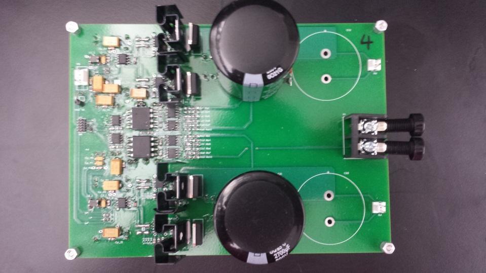
61 47 Figure 5-3. System architecture of the hardware test Figure 5-4. Photo of sub-module board


62 48 Figure 5-5. Photo of sensor board Figure 5-6. Photo of interface board with DSP board and FPGA board
Design, Control and Protection of Modular Multilevel Converter (MMC)-Based Multi- Terminal HVDC System
-Based Multi- Terminal HVDC System") University of Tennessee, Knoxville Trace: Tennessee Research and Creative Exchange Doctoral Dissertations Graduate School 12-216 Design, Control and Protection of Modular Multilevel Converter (MMC)-Based
University of Tennessee, Knoxville Trace: Tennessee Research and Creative Exchange Doctoral Dissertations Graduate School 12-216 Design, Control and Protection of Modular Multilevel Converter (MMC)-Based
Analysis of Modulation and Voltage Balancing Strategies for Modular Multilevel Converters
 University of South Carolina Scholar Commons Theses and Dissertations 1-1-2013 Analysis of Modulation and Voltage Balancing Strategies for Modular Multilevel Converters Ryan Blackmon University of South
IMPORTANCE OF VSC IN HVDC
 IMPORTANCE OF VSC IN HVDC Snigdha Sharma (Electrical Department, SIT, Meerut) ABSTRACT The demand of electrical energy has been increasing day by day. To meet these high demands, reliable and stable transmission
This is the published version of a paper presented at EPE 14-ECCE Europe. Citation for the original published paper:
 http://www.diva-portal.org This is the published version of a paper presented at EPE 14-ECCE Europe. Citation for the original published paper: Ahmad Khan, N., Vanfretti, L., Li, W. (214) Hybrid Nearest
AEIJST - July Vol 3 - Issue 7 ISSN A Review of Modular Multilevel Converter based STATCOM Topology
 A Review of Modular Multilevel Converter based STATCOM Topology * Ms. Bhagyashree B. Thool ** Prof. R.G. Shriwastva *** Prof. K.N. Sawalakhe * Dept. of Electrical Engineering, S.D.C.O.E, Selukate, Wardha,
MMC based D-STATCOM for Different Loading Conditions
 International Journal of Engineering Research And Management (IJERM) ISSN : 2349-2058, Volume-02, Issue-12, December 2015 MMC based D-STATCOM for Different Loading Conditions D.Satish Kumar, Geetanjali
Analysis and loss estimation of different multilevel DC-DC converter modules and different proposed multilevel DC-DC converter systems
 The University of Toledo The University of Toledo Digital Repository Theses and Dissertations 2014 Analysis and loss estimation of different multilevel DC-DC converter modules and different proposed multilevel
Investigation of negative sequence injection capability in H-bridge Multilevel STATCOM
 Investigation of negative sequence injection capability in H-bridge Multilevel STATCOM Ehsan Behrouzian 1, Massimo Bongiorno 1, Hector Zelaya De La Parra 1,2 1 CHALMERS UNIVERSITY OF TECHNOLOGY SE-412
The University of Nottingham
 The University of Nottingham Power Electronic Converters for HVDC Applications Prof Pat Wheeler Power Electronics, Machines and Control (PEMC) Group UNIVERSITY OF NOTTINGHAM, UK Email pat.wheeler@nottingham.ac.uk
THE SUB-MODULE CAPACITANCE AND ARM INDUCTANCE SELECTION IN MODULAR MULTI-LEVEL CONVERTER
 THE SUB-MODULE CAPACITANCE AND ARM INDUCTANCE SELECTION IN MODULAR MULTI-LEVEL CONVERTER 1 Isa Ibrahim, 2 Abubakar Abdullahi Umar, 3 Sani Tijjani, 4 Mujahid Ado Alkassim 5 Nuhu A. Muhammad 1,2,3 Computer
29 Level H- Bridge VSC for HVDC Application
 29 Level H- Bridge VSC for HVDC Application Syamdev.C.S 1, Asha Anu Kurian 2 PG Scholar, SAINTGITS College of Engineering, Kottayam, Kerala, India 1 Assistant Professor, SAINTGITS College of Engineering,
Design, Control and Application of Modular Multilevel Converters for HVDC Transmission Systems by Kamran Sharifabadi, Lennart Harnefors, Hans-Peter
 1 Design, Control and Application of Modular Multilevel Converters for HVDC Transmission Systems by Kamran Sharifabadi, Lennart Harnefors, Hans-Peter Nee, Staffan Norrga, Remus Teodorescu ISBN-10: 1118851560
Multilevel Inverter Based Statcom For Power System Load Balancing System
 IOSR Journal of Electronics and Communication Engineering (IOSR-JECE) e-issn: 2278-2834,p- ISSN: 2278-8735 PP 36-43 www.iosrjournals.org Multilevel Inverter Based Statcom For Power System Load Balancing
CHAPTER 3 SINGLE SOURCE MULTILEVEL INVERTER
 42 CHAPTER 3 SINGLE SOURCE MULTILEVEL INVERTER 3.1 INTRODUCTION The concept of multilevel inverter control has opened a new avenue that induction motors can be controlled to achieve dynamic performance
Size Selection Of Energy Storing Elements For A Cascade Multilevel Inverter STATCOM
 Size Selection Of Energy Storing Elements For A Cascade Multilevel Inverter STATCOM Dr. Jagdish Kumar, PEC University of Technology, Chandigarh Abstract the proper selection of values of energy storing
MMC (Modular Multilevel Converter)
") MMC (Modular Multilevel Converter) Lisbon September 29 2017 Susana Apiñániz Smart Grids Energy and environment Division Tecnalia susana.apinaniz@tecnalia.com INDEX 1. General information 2. Power sub-modules
MMC (Modular Multilevel Converter) Lisbon September 29 2017 Susana Apiñániz Smart Grids Energy and environment Division Tecnalia susana.apinaniz@tecnalia.com INDEX 1. General information 2. Power sub-modules
Modelling of Modular Multilevel Converter Using Input Admittance Approach
 Modelling of Modular Multilevel Converter Using Input Admittance Approach Chalmers University of Technology Division of Electric Power Engineering Master s Thesis in Electric Power Engineering ADULIS ABUN
OPERATION AND CONTROL OF AN ALTERNATE ARM MODULAR MULTILEVEL CONVERTER
 OPERATION AND CONTROL OF AN ALTERNATE ARM MODULAR MULTILEVEL CONVERTER J. M. Kharade 1 and A. R. Thorat 2 1 Department of Electrical Engineering, Rajarambapu Institute of Technology, Islampur, India 2
Introduction to HVDC Transmission. High Voltage Direct Current (HVDC) Transmission
 Transmission") Lecture 29 Introduction to HVDC Transmission Series Compensation 1 Fall 2003 High Voltage Direct Current (HVDC) Transmission Update to Edison s Vision AC Power Generation at Relatively Lower Voltage» Step
Lecture 29 Introduction to HVDC Transmission Series Compensation 1 Fall 2003 High Voltage Direct Current (HVDC) Transmission Update to Edison s Vision AC Power Generation at Relatively Lower Voltage» Step
Literature Review. Chapter 2
 Chapter 2 Literature Review Research has been carried out in two ways one is on the track of an AC-AC converter and other is on track of an AC-DC converter. Researchers have worked in AC-AC conversion
PUBLICATIONS OF PROBLEMS & APPLICATION IN ENGINEERING RESEARCH - PAPER CSEA2012 ISSN: ; e-issn:
 POWER FLOW CONTROL BY USING OPTIMAL LOCATION OF STATCOM S.B. ARUNA Assistant Professor, Dept. of EEE, Sree Vidyanikethan Engineering College, Tirupati aruna_ee@hotmail.com 305 ABSTRACT In present scenario,
DC-LINK CURRENT RIPPLE ELIMINATION & BALANCING OF CAPACITOR VOLTAGE BY USING PHASE SHIFTED CARRIER PWM FOR MODULAR MULTILEVEL CONVERTER
 DC-LINK CURRENT RIPPLE ELIMINATION & BALANCING OF CAPACITOR VOLTAGE BY USING PHASE SHIFTED CARRIER PWM FOR MODULAR MULTILEVEL CONVERTER K Venkata Ravi Kumar PG scholar, Rajeev Gandhi Memorial College of
M.Tech in Industrial Electronics, SJCE, Mysore, 2 Associate Professor, Dept. of ECE, SJCE, Mysore
 Implementation of Five Level Buck Converter for High Voltage Application Manu.N.R 1, V.Nattarasu 2 1 M.Tech in Industrial Electronics, SJCE, Mysore, 2 Associate Professor, Dept. of ECE, SJCE, Mysore Abstract-
2-Dimensional Control of VSC-HVDC
 2-Dimensional Control of VSC-HVDC Master Thesis Magnus Svean, Astrid Thoen Aalborg University Department of Energy Technology Copyright Aalborg University 2018 Title: 2-Dimensional Control of HVDC Semester:
Comparison of Hybrid Asymmetric and Conventional Multilevel Inverters for Medium Voltage Drive Applications
 Comparison of Hybrid Asymmetric and Conventional Multilevel Inverters for Medium Voltage Drive Applications Master of Science Thesis in the Master s programme Electric Power Engineering AMIR SAJJAD BAHMAN
CHAPTER 4 MODIFIED H- BRIDGE MULTILEVEL INVERTER USING MPD-SPWM TECHNIQUE
 58 CHAPTER 4 MODIFIED H- BRIDGE MULTILEVEL INVERTER USING MPD-SPWM TECHNIQUE 4.1 INTRODUCTION Conventional voltage source inverter requires high switching frequency PWM technique to obtain a quality output
Control of MMC in HVDC Applications
 Department of Energy Technology Aalborg University, Denmark Control of MMC in HVDC Applications Master Thesis 30/05/2013 Artjoms Timofejevs Daniel Gamboa Title: Semester: Control of MMC in HVDC applications
THE ALTERNATE ARM CONVERTER: A NEW HYBRID MULTILEVEL CONVERTER WITH DC- FAULT BLOCKING CAPABILITY
 THE ALTERNATE ARM CONVERTER: A NEW HYBRID MULTILEVEL CONVERTER WITH DC- FAULT BLOCKING CAPABILITY Miss.Yashoda.R.Perkar 1, Mr.Santhosh Kumar Rayarao 2 1 P.G. Student, 2 Asst. Prof., Department of Electrical
A Novel Control Method for Input Output Harmonic Elimination of the PWM Boost Type Rectifier Under Unbalanced Operating Conditions
 IEEE TRANSACTIONS ON POWER ELECTRONICS, VOL. 16, NO. 5, SEPTEMBER 2001 603 A Novel Control Method for Input Output Harmonic Elimination of the PWM Boost Type Rectifier Under Unbalanced Operating Conditions
A New Network Proposal for Fault-Tolerant HVDC Transmission Systems
 A New Network Proposal for Fault-Tolerant HVDC Transmission Systems Malothu Malliswari 1, M. Srinu 2 1 PG Scholar, Anurag Engineering College 2 Assistant Professor, Anurag Engineering College Abstract:
DOWNLOAD PDF POWER ELECTRONICS DEVICES DRIVERS AND APPLICATIONS
 Chapter 1 : Power Electronics Devices, Drivers, Applications, and Passive theinnatdunvilla.com - Google D Download Power Electronics: Devices, Drivers and Applications By B.W. Williams - Provides a wide
THE first use of direct current for electrical power transmission
 18 IEEE TRANSACTIONS ON POWER ELECTRONICS, VOL. 30, NO. 1, JANUARY 2015 Modular Multilevel Converters for HVDC Applications: Review on Converter Cells and Functionalities Alireza Nami, Member, IEEE, Jiaqi
FPGA-based Implementation of Modular Multilevel Converter Model for Real-time Simulation of Electromagnetic Transients
 FPGA-based Implementation of Modular Multilevel Converter Model for Real-time Simulation of Electromagnetic Transients Mahmoud Matar, Dominic Paradis and Reza Iravani Abstract-- This paper presents the
SEVERAL static compensators (STATCOM s) based on
 based on") 1118 IEEE TRANSACTIONS ON INDUSTRY APPLICATIONS, VOL. 35, NO. 5, SEPTEMBER/OCTOBER 1999 A New Type of STATCOM Based on Cascading Voltage-Source Inverters with Phase-Shifted Unipolar SPWM Yiqiao Liang,
1118 IEEE TRANSACTIONS ON INDUSTRY APPLICATIONS, VOL. 35, NO. 5, SEPTEMBER/OCTOBER 1999 A New Type of STATCOM Based on Cascading Voltage-Source Inverters with Phase-Shifted Unipolar SPWM Yiqiao Liang,
SHUNT ACTIVE POWER FILTER
 75 CHAPTER 4 SHUNT ACTIVE POWER FILTER Abstract A synchronous logic based Phase angle control method pulse width modulation (PWM) algorithm is proposed for three phase Shunt Active Power Filter (SAPF)
PSPWM Control Strategy and SRF Method of Cascaded H-Bridge MLI based DSTATCOM for Enhancement of Power Quality
 PSPWM Control Strategy and SRF Method of Cascaded H-Bridge MLI based DSTATCOM for Enhancement of Power Quality P.Padmavathi, M.L.Dwarakanath, N.Sharief, K.Jyothi Abstract This paper presents an investigation
Comparative Analysis of Control Strategies for Modular Multilevel Converters
 IEEE PEDS 2011, Singapore, 5-8 December 2011 Comparative Analysis of Control Strategies for Modular Multilevel Converters A. Lachichi 1, Member, IEEE, L. Harnefors 2, Senior Member, IEEE 1 ABB Corporate
IN THE high power isolated dc/dc applications, full bridge
 354 IEEE TRANSACTIONS ON POWER ELECTRONICS, VOL. 21, NO. 2, MARCH 2006 A Novel Zero-Current-Transition Full Bridge DC/DC Converter Junming Zhang, Xiaogao Xie, Xinke Wu, Guoliang Wu, and Zhaoming Qian,
Chapter 2 Shunt Active Power Filter
 Chapter 2 Shunt Active Power Filter In the recent years of development the requirement of harmonic and reactive power has developed, causing power quality problems. Many power electronic converters are
Alternate Arm Converter Operation of the Modular Multilevel Converter
 Alternate Arm Converter Operation of the Modular Multilevel Converter M.M.C. Merlin, P.D. Judge, T.C. Green, P.D. Mitcheson Imperial College London London, UK michael.merlin@imperial.ac.uk Abstract A new
Seven-level cascaded ANPC-based multilevel converter
 University of Wollongong Research Online Faculty of Engineering and Information Sciences - Papers: Part A Faculty of Engineering and Information Sciences Seven-level cascaded ANPC-based multilevel converter
A Comparative Study of Different Topologies of Multilevel Inverters
 A Comparative Study of Different Topologies of Multilevel Inverters Jainy Bhatnagar 1, Vikramaditya Dave 2 1 Department of Electrical Engineering, CTAE (India) 2 Department of Electrical Engineering, CTAE
THE greatest drawback of modular multilevel topologies,
 IEEE TRANSACTIONS ON POWER ELECTRONICS, VOL. 31, NO. 10, OCTOBER 2016 6765 Letters Quasi Two-Level PWM Operation of an MMC Phase Leg With Reduced Module Capacitance Axel Mertens and Jakub Kucka Abstract
High Voltage DC Transmission 2
 High Voltage DC Transmission 2 1.0 Introduction Interconnecting HVDC within an AC system requires conversion from AC to DC and inversion from DC to AC. We refer to the circuits which provide conversion
VOLTAGE BALANCING TECHNIQUES FOR FLYING CAPACITORS USED IN SOFT-SWITCHING MULTILEVEL ACTIVE POWER FILTERS
 VOLTAGE BALANCING TECHNIQUES FOR FLYING CAPACITORS USED IN SOFT-SWITCHING MULTILEVEL ACTIVE POWER FILTERS Byeong-Mun Song Dissertation submitted to the Faculty of the Virginia Polytechnic Institute and
CONVERTERS IN POWER VOLTAGE-SOURCED SYSTEMS. Modeling, Control, and Applications IEEE UNIVERSITATSBIBLIOTHEK HANNOVER. Amirnaser Yazdani.
 VOLTAGE-SOURCED CONVERTERS IN POWER SYSTEMS Modeling, Control, and Applications Amirnaser Yazdani University of Western Ontario Reza Iravani University of Toronto r TECHNISCHE INFORMATIONSBIBLIOTHEK UNIVERSITATSBIBLIOTHEK
Australian Journal of Basic and Applied Sciences. Simulation and Analysis of Closed loop Control of Multilevel Inverter fed AC Drives
 AENSI Journals Australian Journal of Basic and Applied Sciences ISSN:1991-8178 Journal home page: www.ajbasweb.com Simulation and Analysis of Closed loop Control of Multilevel Inverter fed AC Drives 1
Phase Shift Modulation of a Single Dc Source Cascaded H-Bridge Multilevel Inverter for Capacitor Voltage Regulation with Equal Power Distribution
 Phase Shift Modulation of a Single Dc Source Cascaded H-Bridge Multilevel Inverter for Capacitor Voltage Regulation with Equal Power Distribution K.Srilatha 1, Prof. V.Bugga Rao 2 M.Tech Student, Department
Improvement Voltage Sag And Swell Under Various Abnormal Condition Using Series Compensation
 Improvement Voltage Sag And Swell Under Various Abnormal Condition Using Series Compensation Sumit Borakhade #1, Sumit Dabhade *2, Pravin Nagrale #3 # Department of Electrical Engineering, DMIETR Wardha.
ISSN: [Kumaravat * et al., 7(1): January, 2018] Impact Factor: 5.164
![ISSN: [Kumaravat * et al., 7(1): January, 2018] Impact Factor: 5.164](/thumbs/96/128298480.jpg "ISSN: [Kumaravat * et al., 7(1): January, 2018] Impact Factor: 5.164") IJESRT INTERNATIONAL JOURNAL OF ENGINEERING SCIENCES & RESEARCH TECHNOLOGY A REVIEW ARTICLE OF MULTILEVEL INVERTER CONFRIGURATION 4 POLE INDUCTION MOTOR WITH SINGLE DC LINK Piyush Kumaravat *1 & Anil Kumar
IJESRT INTERNATIONAL JOURNAL OF ENGINEERING SCIENCES & RESEARCH TECHNOLOGY A REVIEW ARTICLE OF MULTILEVEL INVERTER CONFRIGURATION 4 POLE INDUCTION MOTOR WITH SINGLE DC LINK Piyush Kumaravat *1 & Anil Kumar
Control of buck-boost chopper type AC voltage regulator
 International Journal of Research in Advanced Engineering and Technology ISSN: 2455-0876; Impact Factor: RJIF 5.44 www.engineeringresearchjournal.com Volume 2; Issue 3; May 2016; Page No. 52-56 Control
Research on Parallel Interleaved Inverters with Discontinuous Space-Vector Modulation *
 Energy and Power Engineering, 2013, 5, 219-225 doi:10.4236/epe.2013.54b043 Published Online July 2013 (http://www.scirp.org/journal/epe) Research on Parallel Interleaved Inverters with Discontinuous Space-Vector
Comparison between Conventional and Modified Cascaded H-Bridge Multilevel Inverter-Fed Drive
 Comparison between Conventional and Modified Cascaded H-Bridge Multilevel Inverter-Fed Drive Gleena Varghese 1, Tissa Tom 2, Jithin K Sajeev 3 PG Student, Dept. of Electrical and Electronics Engg., St.Joseph
CHAPTER 1 INTRODUCTION
 CHAPTER 1 INTRODUCTION 1.1 Introduction Power semiconductor devices constitute the heart of the modern power electronics, and are being extensively used in power electronic converters in the form of a
A Novel Cascaded Multilevel Inverter Using A Single DC Source
 A Novel Cascaded Multilevel Inverter Using A Single DC Source Nimmy Charles 1, Femy P.H 2 P.G. Student, Department of EEE, KMEA Engineering College, Cochin, Kerala, India 1 Associate Professor, Department
Aalborg Universitet. Design and Control of A DC Grid for Offshore Wind Farms Deng, Fujin. Publication date: 2012
 Aalborg Universitet Design and Control of A DC Grid for Offshore Wind Farms Deng, Fujin Publication date: 2012 Document Version Publisher's PDF, also known as Version of record Link to publication from
TRANSFORMER LESS H6-BRIDGE CASCADED STATCOM WITH STAR CONFIGURATION FOR REAL AND REACTIVE POWER COMPENSATION
 International Journal of Technology and Engineering System (IJTES) Vol 8. No.1 Jan-March 2016 Pp. 01-05 gopalax Journals, Singapore available at : www.ijcns.com ISSN: 0976-1345 TRANSFORMER LESS H6-BRIDGE
INSTANTANEOUS POWER CONTROL OF D-STATCOM FOR ENHANCEMENT OF THE STEADY-STATE PERFORMANCE
 INSTANTANEOUS POWER CONTROL OF D-STATCOM FOR ENHANCEMENT OF THE STEADY-STATE PERFORMANCE Ms. K. Kamaladevi 1, N. Mohan Murali Krishna 2 1 Asst. Professor, Department of EEE, 2 PG Scholar, Department of
CHAPTER 5 POWER QUALITY IMPROVEMENT BY USING POWER ACTIVE FILTERS
 86 CHAPTER 5 POWER QUALITY IMPROVEMENT BY USING POWER ACTIVE FILTERS 5.1 POWER QUALITY IMPROVEMENT This chapter deals with the harmonic elimination in Power System by adopting various methods. Due to the
IJSRD - International Journal for Scientific Research & Development Vol. 2, Issue 07, 2014 ISSN (online):
:") IJSRD - International Journal for Scientific Research & Development Vol. 2, Issue 07, 2014 ISSN (online): 2321-0613 Control and Analysis of VSC based High Voltage DC Transmission Tripti Shahi 1 K.P.Singh
IJSRD - International Journal for Scientific Research & Development Vol. 2, Issue 07, 2014 ISSN (online): 2321-0613 Control and Analysis of VSC based High Voltage DC Transmission Tripti Shahi 1 K.P.Singh
CHAPTER 2 A SERIES PARALLEL RESONANT CONVERTER WITH OPEN LOOP CONTROL
 14 CHAPTER 2 A SERIES PARALLEL RESONANT CONVERTER WITH OPEN LOOP CONTROL 2.1 INTRODUCTION Power electronics devices have many advantages over the traditional power devices in many aspects such as converting
Lecture Note. DC-AC PWM Inverters. Prepared by Dr. Oday A Ahmed Website: https://odayahmeduot.wordpress.com
 Lecture Note 10 DC-AC PWM Inverters Prepared by Dr. Oday A Ahmed Website: https://odayahmeduot.wordpress.com Email: 30205@uotechnology.edu.iq Scan QR DC-AC PWM Inverters Inverters are AC converters used
Variable Voltage Source Equivalent Model of Modular Multilevel Converter
 International Journal of Research in Engineering and Science (IJRES) ISSN (Online): 30-9364, ISSN (Print): 30-9356 Volume 3 Issue 11 ǁ November. 015 ǁ PP.49-54 Variable Voltage Source Equivalent Model
Modular Multilevel Dc/Dc Converters with Phase-Shift Control Scheme for High-Voltage Dc-Based Systems
 Modular Multilevel Dc/Dc Converters with Phase-Shift Control Scheme for High-Voltage Dc-Based Systems Mr.AWEZ AHMED Master of Technology (PG scholar) AL-HABEEB COLLEGE OF ENGINEERING AND TECHNOLOGY, CHEVELLA.
A Novel Single-Stage Push Pull Electronic Ballast With High Input Power Factor
 770 IEEE TRANSACTIONS ON INDUSTRIAL ELECTRONICS, VOL. 48, NO. 4, AUGUST 2001 A Novel Single-Stage Push Pull Electronic Ballast With High Input Power Factor Chang-Shiarn Lin, Member, IEEE, and Chern-Lin
Enhanced Performance of Multilevel Inverter Fed Induction Motor Drive
 Enhanced Performance of Multilevel Inverter Fed Induction Motor Drive Venkata Anil Babu Polisetty 1, B.R.Narendra 2 PG Student [PE], Dept. of EEE, DVR. & Dr.H.S.MIC College of Technology, AP, India 1 Associate
Chapter -3 ANALYSIS OF HVDC SYSTEM MODEL. Basically the HVDC transmission consists in the basic case of two
 Chapter -3 ANALYSIS OF HVDC SYSTEM MODEL Basically the HVDC transmission consists in the basic case of two convertor stations which are connected to each other by a transmission link consisting of an overhead
International Journal of Emerging Technology in Computer Science & Electronics (IJETCSE) ISSN: Volume 8 Issue 1 APRIL 2014.
 ISSN: Volume 8 Issue 1 APRIL 2014.") WIND TURBINE VOLTAGE STABILITY USING FACTS DEVICE PRAVEEN KUMAR.R# and C.VENKATESH KUMAR* #M.E.POWER SYSTEMS ENGINEERING, EEE, St. Joseph s college of engineering, Chennai, India. *Asst.Professor, Department
WIND TURBINE VOLTAGE STABILITY USING FACTS DEVICE PRAVEEN KUMAR.R# and C.VENKATESH KUMAR* #M.E.POWER SYSTEMS ENGINEERING, EEE, St. Joseph s college of engineering, Chennai, India. *Asst.Professor, Department
Overview of Actuation Thrust
 Overview of Actuation Thrust Fred Wang Thrust Leader, UTK Professor ECE 620 CURENT Course September 13, 2017 Actuation in CURENT Wide Area Control of Power Power Grid Grid Measurement &Monitoring HVDC
A Hybrid Cascaded Multilevel Inverter for Interfacing with Renewable Energy Resources
 A Hybrid Cascaded Multilevel Inverter for Interfacing with Renewable Energy Resources P.Umapathi Reddy 1, S.Sivanaga Raju 2 Professor, Dept. of EEE, Sree Vidyanikethan Engineering College, Tirupati, A.P.
Harmonic elimination control of a five-level DC- AC cascaded H-bridge hybrid inverter
 University of Wollongong Research Online Faculty of Engineering and Information Sciences - Papers Faculty of Engineering and Information Sciences 2 Harmonic elimination control of a five-level DC- AC cascaded
SUPERCONDUCTING MAGNETIC ENERGY
 1360 IEEE TRANSACTIONS ON APPLIED SUPERCONDUCTIVITY, VOL. 20, NO. 3, JUNE 2010 SMES Based Dynamic Voltage Restorer for Voltage Fluctuations Compensation Jing Shi, Yuejin Tang, Kai Yang, Lei Chen, Li Ren,
5-Level Parallel Current Source Inverter for High Power Application with DC Current Balance Control
 2011 IEEE International Electric Machines & Drives Conference (IEMDC) 5-Level Parallel Current Source Inverter for High Power Application with DC Current Balance Control N. Binesh, B. Wu Department of
CAPACITOR VOLTAGE BALANCING IN SINGLE PHASE SEVEN-LEVEL PWM INVERTER
 Journal of Research in Engineering and Applied Sciences CAPACITOR VOLTAGE BALANCING IN SINGLE PHASE SEVEN-LEVEL PWM INVERTER Midhun G, 2Aleena T Mathew Assistant Professor, Department of EEE, PG Student
Acknowledgements Introduction p. 1 Electric Power Quality p. 3 Impacts of Power Quality Problems on End Users p. 4 Power Quality Standards p.
 Preface p. xv Acknowledgements p. xix Introduction p. 1 Electric Power Quality p. 3 Impacts of Power Quality Problems on End Users p. 4 Power Quality Standards p. 6 Power Quality Monitoring p. 7 Power
The Influence of Odevity of Carrier Ratio on Three-level Rectifier Wang Pengzhan1, a, Luo Wei2, Yang Shasha1, Cao Tianzhi3 and Li Huawei1
 4th International Conference on Machinery, Materials and Information Technology Applications (ICMMITA 216) The Influence of Odevity of Carrier Ratio on Three-level Rectifier Wang Pengzhan1, a, Luo Wei2,
OVERVIEW OF SVC AND STATCOM FOR INSTANTANEOUS POWER CONTROL AND POWER FACTOR IMPROVEMENT
 OVERVIEW OF SVC AND STATCOM FOR INSTANTANEOUS POWER CONTROL AND POWER FACTOR IMPROVEMENT Harshkumar Sharma 1, Gajendra Patel 2 1 PG Scholar, Electrical Department, SPCE, Visnagar, Gujarat, India 2 Assistant
CHAPTER 2 CURRENT SOURCE INVERTER FOR IM CONTROL
 9 CHAPTER 2 CURRENT SOURCE INVERTER FOR IM CONTROL 2.1 INTRODUCTION AC drives are mainly classified into direct and indirect converter drives. In direct converters (cycloconverters), the AC power is fed
Dr.Arkan A.Hussein Power Electronics Fourth Class. 3-Phase Voltage Source Inverter With Square Wave Output
 3-Phase Voltage Source Inverter With Square Wave Output ١ fter completion of this lesson the reader will be able to: (i) (ii) (iii) (iv) Explain the operating principle of a three-phase square wave inverter.
Hybrid Simulation of ±500 kv HVDC Power Transmission Project Based on Advanced Digital Power System Simulator
 66 JOURNAL OF ELECTRONIC SCIENCE AND TECHNOLOGY, VOL. 11, NO. 1, MARCH 213 Hybrid Simulation of ±5 kv HVDC Power Transmission Project Based on Advanced Digital Power System Simulator Lei Chen, Kan-Jun
Power Quality enhancement of a distribution line with DSTATCOM
 ower Quality enhancement of a distribution line with DSTATCOM Divya arashar 1 Department of Electrical Engineering BSACET Mathura INDIA Aseem Chandel 2 SMIEEE,Deepak arashar 3 Department of Electrical
A COMPARITIVE STUDY OF THREE LEVEL INVERTER USING VARIOUS TOPOLOGIES
 A COMPARITIVE STUDY OF THREE LEVEL INVERTER USING VARIOUS TOPOLOGIES Swathy C S 1, Jincy Mariam James 2 and Sherin Rachel chacko 3 1 Assistant Professor, Dept. of EEE, Sree Buddha College of Engineering
Efficient Modeling of Modular Multilevel Converters for Fast Simulation of Large-Scale MMC-HVDC Embedded Power Systems
 Efficient Modeling of Modular Multilevel Converters for Fast Simulation of Large-Scale MMC-HVDC Embedded Power Systems Final Project Report S-78G Power Systems Engineering Research Center Empowering Minds
Multi Level Inverter Based Active Power Filter for Harmonic Reduction
 Multi Level Inverter Based Active Power Filter for Harmonic Reduction K Siva Gopi Raju Department of Electrical and Electronics Engineering, Andhra University, Visakhapatnam, Andhra Pradesh 530003, India.
Laboratory Investigation of Variable Speed Control of Synchronous Generator With a Boost Converter for Wind Turbine Applications
 Laboratory Investigation of Variable Speed Control of Synchronous Generator With a Boost Converter for Wind Turbine Applications Ranjan Sharma Technical University of Denmark ransharma@gmail.com Tonny
International Journal of Emerging Researches in Engineering Science and Technology, Volume 1, Issue 2, December 14
 CONTROL STRATEGIES FOR A HYBRID MULTILEEL INERTER BY GENERALIZED THREE- DIMENSIONAL SPACE ECTOR MODULATION J.Sevugan Rajesh 1, S.R.Revathi 2 1. Asst.Professor / EEE, Kalaivani college of Techonology, Coimbatore,
e-issn: p-issn:
 Available online at www.ijiere.com International Journal of Innovative and Emerging Research in Engineering e-issn: 2394-3343 p-issn: 2394-5494 PFC Boost Topology Using Average Current Control Method Gemlawala
The Modular Multilevel Converter
 The Modular Multilevel Converter presented by Josep Pou Assoc. Professor, IEEE Fellow Program Director Power Electronics, Energy Research Institute at NTU (ERI@N) Co-Director, Electrical Rolls-Royce Corp
Modeling and Control of Single Phase Grid-Tie Converters
 University of Tennessee, Knoxville Trace: Tennessee Research and Creative Exchange Masters Theses Graduate School 8-1 Modeling and Control of Single Phase Grid-Tie Converters Bradford Christopher Trento
A NOVEL APPROACH TO ENHANCE THE POWER QUALITY USING CMLI BASED CUSTOM POWER DEVICES
 A NOVEL APPROACH TO ENHANCE THE POWER QUALITY USING CMLI BASED CUSTOM POWER DEVICES 1 M. KAVITHA, 2 A. SREEKANTH REDDY & 3 D. MOHAN REDDY Department of Computational Engineering, RGUKT, RK Valley, Kadapa
Design of a Modular Multilevel Converter as an Active Front-End for a magnet supply application
 CERN-ACC-015-0009 k.papastergiou@cern.ch Design of a Modular Multilevel Converter as an Active Front-End for a magnet supply application 1 Panagiotis Asimakopoulos, 1 Konstantinos Papastergiou, Massimo
CHAPTER 4 4-PHASE INTERLEAVED BOOST CONVERTER FOR RIPPLE REDUCTION IN THE HPS
 71 CHAPTER 4 4-PHASE INTERLEAVED BOOST CONVERTER FOR RIPPLE REDUCTION IN THE HPS 4.1 INTROUCTION The power level of a power electronic converter is limited due to several factors. An increase in current
IEEE 2011 Electrical Power and Energy Conference
 1. Research Background 2. Fault Characteristics of Internal AC Bus faults 3. Fault Characteristics of DC faults 4. Requirements for protection 5. Conclusions Fig. 1. Topology of modular mul2level converter.
PERFORMANCE ANALYSIS OF SOLAR POWER GENERATION SYSTEM WITH A SEVEN-LEVEL INVERTER SUDHEER KUMAR Y, PG STUDENT CHANDRA KIRAN S, ASSISTANT PROFESSOR
 PERFORMANCE ANALYSIS OF SOLAR POWER GENERATION SYSTEM WITH A SEVEN-LEVEL INVERTER SUDHEER KUMAR Y, PG STUDENT CHANDRA KIRAN S, ASSISTANT PROFESSOR KV SUBBA REDDY INSTITUTE OF TECHNOLOGY, KURNOOL Abstract:
Overview of Actuation Thrust
 Overview of Actuation Thrust Fred Wang Thrust Leader, UTK Professor Prepared for CURENT Course September 4, 2013 Actuation in CURENT Wide Area Control of Power Power Grid Grid Measurement &Monitoring HVDC
Multilevel Inverter with Coupled Inductors with Sine PWM Techniques
 Multilevel Inverter with Coupled Inductors with Sine PWM Techniques S.Subalakshmi 1, A.Mangaiyarkarasi 2, T.Jothi 3, S.Rajeshwari 4 Assistant Professor-I, Dept. of EEE, Prathyusha Institute of Technology
Simulation of Three Phase Cascaded H Bridge Inverter for Power Conditioning Using Solar Photovoltaic System
 Simulation of Three Phase Cascaded H Bridge Inverter for Power Conditioning Using Solar Photovoltaic System 1 G.Balasundaram, 2 Dr.S.Arumugam, 3 C.Dinakaran 1 Research Scholar - Department of EEE, St.
Published by: PIONEER RESEARCH & DEVELOPMENT GROUP(www.prdg.org)
") A High Power Density Single Phase Pwm Rectifier with Active Ripple Energy Storage A. Guruvendrakumar 1 and Y. Chiranjeevi 2 1 Student (Power Electronics), EEE Department, Sathyabama University, Chennai,
A High Power Density Single Phase Pwm Rectifier with Active Ripple Energy Storage A. Guruvendrakumar 1 and Y. Chiranjeevi 2 1 Student (Power Electronics), EEE Department, Sathyabama University, Chennai,
MLI HYBRID STATCOM WITH WIDE COMPENSATION RANGE AND LOW DC LINK VOLTAGE
 MLI HYBRID STATCOM WITH WIDE COMPENSATION RANGE AND LOW DC LINK VOLTAGE #1 BONDALA DURGA, PG SCHOLAR #2 G. ARUNA LAKSHMI, ASSISTANT PROFESSOR DEPARTMENT OF ELECTRICAL AND ELECTRONICS ENGINEERING KAKINADA
STATCOM with FLC and Pi Controller for a Three-Phase SEIG Feeding Single-Phase Loads
 STATCOM with FLC and Pi Controller for a Three-Phase SEIG Feeding Single-Phase Loads Ponananthi.V, Rajesh Kumar. B Final year PG student, Department of Power Systems Engineering, M.Kumarasamy College of