TGA2509. Wideband 1W HPA with AGC
|
|
|
- Gilbert Grant
- 5 years ago
- Views:
Transcription


 >29 dbm")

1 Product Description The TriQuint TGA2509 is a compact Wideband High Power Amplifier with AGC. The HPA operates from 2-22 GHz and is designed using TriQuint s proven standard 0.25 um gate phemt production process. The TGA2509 provides >28.5 dbm of output power at 1 db gain compression with small signal gain of 17 db. Typical saturated power is 30 dbm from 2-16 GHz. The TGA2509 is suitable for a variety of wideband electronic warfare systems such as radar warning receivers, electronic counter measures,decoys, jammers and phased array systems. The TGA2509 is 100% DC and RF tested on-wafer to ensure performance compliance. Lead-free and RoHS compliant Wideband 1W HPA with AGC TGA2509 Key Features Frequency Range: 2-22 GHz 30 dbm Nominal Psat (2-16 GHz) >29 dbm Nominal Psat (2-20 GHz) >28.5 dbm Output P1dB 17 db Nominal Gain > 25 db AGC Range 0.25 um 3MI phemt Technology Nominal Bias A Chip Dimensions: 2.30 x 3.20 x 0.10 mm (0.091 x x in) Primary Applications Wideband Gain Block Military EW and ECM Test Equipment Measured Fixtured Data Bias Conditions: Vd =12 V, Id= 1.1 A Datasheet subject to change without notice 1
2 TABLE I MAXIMUM RATINGS 1/ SYMBOL PARAMETER VALUE NOTES V + Positive Supply Voltage 12.5 V 2/ V g1 Gate 1 Supply Voltage Range -2V TO 0 V V g2 Gate 2 Supply Voltage Range -2V TO 0 V V c AGC Control Voltage Range V c < +5 V V + V c < 14V I + Positive Supply Current 1.4 A 2/ I G Gate Supply Current 70 ma P IN Input Continuous Wave Power 30 dbm 2/ P D Power Dissipation (without using AGC) 17.5 W 2/, 3/ P D Power Dissipation (when Vc < +2V) 15.7 W 2/, 3/ T CH Operating Channel Temperature 200 C 4/, 5/ Mounting Temperature (30 Seconds) 320 C T STG Storage Temperature -65 to 150 C 1/ These ratings represent the maximum operable values for this device. 2/ Current is defined under no RF drive conditions. Combinations of supply voltage, supply current, input power, and output power shall not exceed P D. 3/ When operated at this power dissipation with a base plate temperature of 70 C, the median life is 8.2E4 hours (without AGC) or 2.3E4 hours (with AGC). 4/ Junction operating temperature will directly affect the device median time to failure (Tm). For maximum life, it is recommended that junction temperatures be maintained at the lowest possible levels. 5/ These ratings apply to each individual FET. 2
3 TABLE II RF CHARACTERIZATION TABLE (T A = 25 C, Nominal) Vd = 12 V, Id = 1.1 A SYMBOL PARAMETER TEST CONDITION NOMINAL UNITS Gain Small Signal Gain f = 2-22 GHz 17 db IRL Input Return Loss f = 2-22 GHz 12 db ORL Output Return Loss f = 2-22 GHz 12 db Psat Saturated Power f = 2-16 GHz f = 2-20 GHz db P 1dB Output 1dB Gain Compression f = 2-20 GHz 28.5 dbm 3
 (without using AGC) θ JC Thermal Resistance (channel to backside of carrier) Vd = 12 V I D = 0.88 A Pdiss = 10.6 W (when using AGC) θ JC ( C/W) Tm (HRS) 155 6.")

4 TABLE III THERMAL INFORMATION PARAMETER TEST CONDITIONS T CH ( o C) θ JC Thermal Vd = 12 V Resistance I D = 1.1 A (channel to backside Pdiss = 13.2 W of carrier) (without using AGC) θ JC Thermal Resistance (channel to backside of carrier) Vd = 12 V I D = 0.88 A Pdiss = 10.6 W (when using AGC) θ JC ( C/W) Tm (HRS) E E+5 Note: Assumes eutectic attach using 1.5 mil 80/20 AuSn mounted to a 20 mil CuMo Carrier at 70 C baseplate temperature. Worst case is at saturated output power when DC power consumption rises to 15 W with 1 W RF power delivered to load. Power dissipated is 14 W and the temperature rise in the channel is 90 C. Median Lifetime (Tm) vs. Channel Temperature 4

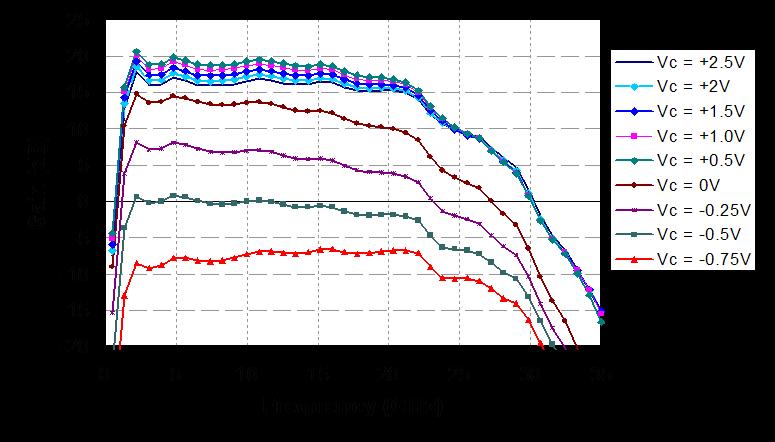
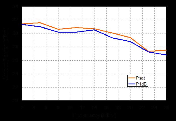
5 Measured Fixtured Data Bias Conditions: Vd =12 V, Id= 1.1 A 5
6 Mechanical Characteristics (0.126) (0.122) (0.011) (0.013) (0.019) (0.004) (0.000) (0.091) (0.087) (0.070) (0.045) (0.014) (0.004) (0.000) Units: millimeters (inches) Thickness: (0.004) Chip edge to bond pad dimensions are shown to center of bond pad Chip size tolerance: +/ (0.002) GND IS BACKSIDE OF MMIC Bond pad #1 (RF In) x (0.004 x 0.006) Bond pad #2 (Vg1) x (0.004 x 0.004) Bond pad #3 (RF Out) x (0.004 x 0.006) Bond pad #4 (Vd) x (0.010 x 0.004) Bond pad #5 (Vg2) x (0.004 x 0.004) Bond pad #6 (VC) x (0.004 x 0.004) GaAs MMIC devices are susceptible to damage from Electrostatic Discharge. Proper precautions should be observed during handling, assembly and test. 6
7 Recommended Assembly Diagram Bias Procedures: Vc bias connection is optional, but the 100pF cap always needs to be connected. Vg1 For biasing without AGC control: 1. Apply -1.2V to Vg1, and -1.2V to Vg2. 2. Apply +12V to Vd. 4. Adjust Vg1 to attain 580 ma drain current (Id) 4. Adjust Vg2 to attain 1080 ma total drain current (Id). 1 uf 100pF For biasing with AGC control: 1. Apply -1.2V to Vg1 and -1.2V to Vg2 2. Apply +12V to Vd 3. Apply +2.6V to Vc 4. Adjust Vg1 to attain 580 ma drain current (Id) 5. Adjust Vg2 to attain 1080 ma total drain current (Id). 6. Adjust Vc as needed to control gain level. RF IN 100pF 100pF 100pF RF OUT 1 uf 1 uf Vc Vg2 Vd To ensure low frequency stability, use 1uF surface mount (not leaded) capacitors (on the Vd, Vg1, and Vg2 nodes) that are located close to the MMIC. Contact TriQuint Semiconductor Applications Engineering for more details. GaAs MMIC devices are susceptible to damage from Electrostatic Discharge. Proper precautions should be observed during handling, assembly and test. 7
8 Assembly Process Notes Reflow process assembly notes: Use AuSn (80/20) solder with limited exposure to temperatures at or above 300 C for 30 sec An alloy station or conveyor furnace with reducing atmosphere should be used. No fluxes should be utilized. Coefficient of thermal expansion matching is critical for long-term reliability. Devices must be stored in a dry nitrogen atmosphere. Component placement and adhesive attachment assembly notes: Vacuum pencils and/or vacuum collets are the preferred method of pick up. Air bridges must be avoided during placement. The force impact is critical during auto placement. Organic attachment can be used in low-power applications. Curing should be done in a convection oven; proper exhaust is a safety concern. Microwave or radiant curing should not be used because of differential heating. Coefficient of thermal expansion matching is critical. Interconnect process assembly notes: Thermosonic ball bonding is the preferred interconnect technique. Force, time, and ultrasonics are critical parameters. Aluminum wire should not be used. Devices with small pad sizes should be bonded with inch wire. Maximum stage temperature is 200 C. GaAs MMIC devices are susceptible to damage from Electrostatic Discharge. Proper precautions should be observed during handling, assembly and test. 8
TGA4830. Wideband Low Noise Amplifier. Key Features and Performance. Measured Performance V + = 5V, I + = 50mA. Primary Applications
 Wideband Low Noise Amplifier Measured Performance V + = 5V, I + = 50mA Key Features and Performance DC - 45GHz Frequency Range 13dB Gain @ 20GHz 15dB Return Loss @ 20GHz 11.5dBm Typical P1dB 3.2dB Typical
17-43 GHz MPA / Multiplier. S-Parameters (db) P1dB (dbm)
 P1dB (dbm)") 17-43 GHz MPA / Multiplier Key Features Frequency: 17-43 GHz 25 db Nominal Gain @ Mid-band 22 dbm Nominal Output P1dB 2x and 3x Multiplier Function.15 um 3MI phemt Technology Chip Dimensions 1.72 x.76
17-43 GHz MPA / Multiplier Key Features Frequency: 17-43 GHz 25 db Nominal Gain @ Mid-band 22 dbm Nominal Output P1dB 2x and 3x Multiplier Function.15 um 3MI phemt Technology Chip Dimensions 1.72 x.76
33-47 GHz Wide Band Driver Amplifier TGA4522
 33-47 GHz Wide Band Driver Amplifier Key Features Frequency Range: 33-47 GHz 27.5 dbm Nominal Psat @ 38GHz 27 dbm P1dB @ 38 GHz 36 dbm OTOI @ Pin = 19 dbm/tone 18 db Nominal Gain @ 38GHz db Nominal Return
Product Data Sheet August 5, 2008
 TriQuint Recommends the TGA4516 be used for New Designs 33-36 GHz 2W Power Amplifier Key Features 0.25 um phemt Technology 17 db Nominal Gain 31 dbm Pout @ P1dB, Psat 33dBm @ 6V, 34dBm @7V Bias 6-7V @
TGP GHz 180 Phase Shifter. Primary Applications. Product Description. Measured Performance
 Amplitude Error (db) S21 (db) 10.0 9.0 8.0 7.0 6.0 5.0 4.0 3.0 2.0 1.0 Measured Performance 0.0 140 30 31 32 33 34 35 36 37 38 39 40 0-1 -2-3 -4-5 State 0-6 State 1-7 -8-9 -10 30 31 32 33 34 35 36 37 38
TGA GHz 2.5 Watt, 25dB Power Amplifier. Key Features and Performance. Preliminary Measured Performance Bias Conditions: Vd=7V Id=640mA
 13-17 GHz 2.5 Watt, 25dB Power Amplifier Preliminary Measured Performance Bias Conditions: Vd=7V Id=640mA Key Features and Performance 34 dbm Midband Pout 25 db Nominal Gain 7 db Typical Input Return Loss
6-13 GHz Low Noise Amplifier TGA8399B-SCC
 6-13 GHz Low Noise Amplifier Key Features and Performance 6-13 GHz Frequency Range 1.5 db Typical Noise Figure Midband 26 db Nominal Gain High Input Power Handling: ~ 20dBm Balanced Input for Low VSWR
12-18 GHz Ku-Band 3-Stage Driver Amplifier TGA2507
 12- GHz Ku-Band 3-Stage Driver Amplifier Key Features 12- GHz Bandwidth 28 db Nominal Gain dbm P1dB Bias: 5,6,7 V, 80 ± 10% ma Self Bias 0.5 um 3MI mmw phemt Technology Chip Dimensions: 1.80 x 0.83 x 0.1
27-31 GHz 2W Balanced Power Amplifier TGA4513
 27-31 GHz 2W Balanced Power Amplifier Key Features 27-31 GHz Bandwidth > 32 dbm P1dB 33 dbm Psat 2 db Nominal Gain IMR3 is 37 dbc @ 18 dbm SCL 14 db Nominal Return Loss Bias: 6 V, 84 ma.25 um 3MI MMW phemt
TGA4801. DC 35 GHz MPA with AGC. Key Features and Performance. Primary Applications: Description
 DC 35 GHz MPA with AGC Key Features and Performance 0.25um phemt Technology DC - 23GHz Linear BW DC - 35GHz Saturated Power BW 14dB Small Signal Gain 10ps Edge Rates (20/80) 7Vpp 43Gb/s NRZ PRBS Amplitude
High Power DC - 18GHz SPDT FET Switch
 High Power DC - 18GHz SPDT FET Switch Key Features and Performance DC - 18 GHz Frequency Range 29 dbm Input P1dB @ V C = -5V > 30 db Isolation
23-29 GHz High Power Amplifier TGA9070-SCC
 23-29 GHz High Power Amplifier TGA9070-SCC Description The TriQuint TGA9070-SCC is a three stage HPA MMIC design using TriQuint s proven 0.25 um Power phemt process to support a variety of millimeter wave
6-18 GHz High Power Amplifier TGA9092-SCC
 6-18 GHz High Power Amplifier Key Features and Performance Dual Channel Power Amplifier 0.25um phemt Technology 6-18 GHz Frequency Range 2.8 W/Channel Midband Pout 5.6 W Pout Combined 24 db Nominal Gain
TGA GHz Low Noise Amplifier with AGC. Key Features
 NF (db) Gain, IRL, ORL (db) 2 2 GHz Low Noise Amplifier with AGC Measured Performance Bias conditions: Vd = V, Id = ma, Vg1 =. V, 2 2 2 2 3 3 9 8 7 6 4 3 2 1 Vg2 = +1.3 V Typical 2 4 6 8 12 14 16 18 2
DC - 20 GHz Discrete power phemt
 DC - 20 GHz Discrete power phemt Product Description The TriQuint is a discrete 0.6 mm phemt which operates from DC-20 GHz. The is designed using TriQuint s proven standard 0.3um power phemt production
Ka-Band 2W Power Amplifier
 Ka-Band 2W Power Amplifier Key Features 30-40 GHz Bandwidth > 33 dbm Nominal Psat @ Pin = 20dBm 18 db Nominal Gain Bias: 6 V, 50 ma Idq (1.9A under RF Drive) 0.15 um 3MI MMW phemt Technology Thermal Spreader
4 Watt Ka-Band HPA Key Features Measured Performance Primary Applications Ka-Band VSAT Product Description
 4 Watt Ka-Band HPA Key Features Frequency Range: 28-31 GHz 3 dbm Nominal Psat Gain: 24 db Return Loss: -8 db Bias: Vd = V, Idq = 1. A, Vg = -.75 V Typical Technology: 3MI.15 um Power phemt Chip Dimensions:
TGA4811. DC - 60 GHz Low Noise Amplifier
 TGA11 DC - GHz Low Noise Amplifier Key Features GHz Bandwidth 3. db noise figure > 15 db small signal gain 13 dbm P1dB +/- 7 ps group delay variation Bias:.5V, 5 ma.15 um 3MI mhemt Technology Chip Dimensions:
27-31 GHz 1W Power Amplifier TGA4509-EPU
 27-31 GHz 1W Power Amplifier Key Features 22 db Nominal Gain @ 30 GHz 30 dbm Nominal Pout @ P1dB 25% PAE @ P1dB -10 db Nominal Return Loss Built-in Power Detector 0.25-µm mmw phemt 3MI Bias Conditions:
10Gb/s Wide Dynamic Range Differential TIA
 10Gb/s Wide Dynamic Range Differential TIA Differential Zt (db-ohm) Preliminary Measured Performance 79 76 73 70 67 64 61 58 55 52 Bias Conditions: V + =3.3V I + =70mA Differential Transimpedance S22 Non-Inverting
TGA Watt Ka-Band HPA. Key Features. Measured Performance Bias conditions: Vd = 6 V, Idq = 3200 ma, Vg = -0.7 V Typical
 7 Watt Ka-Band HPA Key Features Frequency Range: 29-31 GHz 38.5 dbm Nominal Psat, 38 dbm Nominal P1dB Gain: 21 db Return Losses: -10 db Bias: Vd = 6 V, Idq = 3.2 A, Vg = -0.7 V Typical, Id under RF drive
TGF Watt Discrete Power GaN on SiC HEMT. Key Features. Measured Performance. Primary Applications Space Military Broadband Wireless
 6 Watt Discrete Power GaN on SiC HEMT Key Features Frequency Range: DC - 18 GHz > 38 dbm Nominal Psat 55% Maximum PAE 15 db Nominal Power Gain Bias: Vd = 28-40 V, Idq = 125 ma, Vg = -3 V Typical Technology:
TGF Watt Discrete Power GaN on SiC HEMT. Key Features. Measured Performance. Primary Applications Space Military Broadband Wireless
 12 Watt Discrete Power GaN on SiC HEMT Key Features Frequency Range: DC - 18 GHz > 41 dbm Nominal Psat 55% Maximum PAE 15 db Nominal Power Gain Bias: Vd = 28-40 V, Idq = 250 ma, Vg = -3 V Typical Technology:
TGF Watt Discrete Power GaN on SiC HEMT. Key Features. Primary Applications Defense & Aerospace Broadband Wireless. Product Description
 50 Watt Discrete Power GaN on SiC HEMT Key Features Frequency Range: DC - 18 GHz 47 dbm Nominal Psat 55% Maximum PAE 8.7 db Nominal Power Gain Bias: Vd = 28-35 V, Idq = 1 A, Vg = -3.6 V Typical Technology:
High Power Ka-Band SPDT Switch
 High Power Ka-Band SPDT Switch Key Features and Performance 27-46 GHz Frequency Range > 33 dbm Input P1dB @ V C = 7.5V On Chip Biasing Resistors On Chip DC Blocks < 0.9 db Typical Insertion Loss < 4ns
TGA4532 K-Band Power Amplifier
 Applications Point-to-Point Radio Communication Product Features Functional Block Diagram Frequency Range: 17.5 20 GHz Power: 32.5 dbm Psat, 31.5 dbm P1dB Gain: 23 db TOI: 43 dbm @ 22 dbm SCL Return Loss:
TGA4852 DC 35GHz Wideband Amplifier
 Product Description The TriQuint TGA4852 is a medium power wideband AGC MMIC. Drain bias may be applied through the output port for best efficiency or through the on-chip drain termination. RF ports are
TGF Watt Discrete Power GaN on SiC HEMT
 Applications Marine radar Satellite communications Point to point communications Military communications Broadband amplifiers High efficiency amplifiers Product Features Functional Block Diagram Frequency
17-24 GHz Linear Driver Amplifier. S11 and S22 (db) -15
 -15") Pout (dbm) or OTOI (dbm) S21 (db) S11 and S22 (db) 17-24 GHz Linear Driver Amplifier Key Features Frequency Range: 17-24 GHz 25.5 dbm Nominal Psat, 23.5 dbm Nominal P1dB Gain: 20 db OTOI: 33 dbm Typical
Pout (dbm) or OTOI (dbm) S21 (db) S11 and S22 (db) 17-24 GHz Linear Driver Amplifier Key Features Frequency Range: 17-24 GHz 25.5 dbm Nominal Psat, 23.5 dbm Nominal P1dB Gain: 20 db OTOI: 33 dbm Typical
TGA2521-SM GHz Linear Driver Amplifier Key Features Measured Performance
 17-24 GHz Linear Driver Amplifier Key Features Frequency Range: 17-24 GHz 25.5 dbm Nominal Psat, 23.5 dbm Nominal P1dB Gain: 20 db OTOI: 33 dbm Typical Bias: Vd = 5 V, Idq = 320 ma, Vg = -0.5 V Typical
QPA1003D. 1 8 GHz 10 W GaN Power. Product Description. Product Features. Functional Block Diagram. Applications. Ordering Information
 Product Description Qorvo s is a wideband high power MMIC amplifier fabricated on Qorvo s production.15um GaN on SiC process (QGaN15). The operates from 1 8 GHz and typically provides W saturated output
17-35GHz MPA/Multiplier TGA4040SM
 Not Recommended for New Designs Advance Product Information 17-35GHz MPA/Multiplier TriQuint Recommends the TGA43-SM or TGA431-SM be used for New Designs Key Features Product Description The TriQuint TG44SM
TGA2521-SM GHz Linear Driver Amplifier. Key Features. Measured Performance
 17-24 GHz Linear Driver Amplifier Key Features Frequency Range: 17-24 GHz 25.5 dbm Nominal Psat, 23.5 dbm Nominal P1dB Gain: 20 db OTOI: 33 dbm Typical Bias: Vd = 5 V, Idq = 320 ma, Vg = -0.5 V Typical
TGA2521-SM GHz Linear Driver Amplifier. Key Features. Measured Performance
 17-24 GHz Linear Driver Amplifier Key Features Frequency Range: 17-24 GHz 25.5 dbm Nominal Psat, 23.5 dbm Nominal P1dB Gain: 20 db OTOI: 33 dbm Typical Bias: Vd = 5 V, Idq = 320 ma, Vg = -0.5 V Typical
TGF um Discrete GaAs phemt
 Applications Defense & Aerospace High-Reliability Test and Measurement Commercial Broadband Wireless Product Features Functional Block Diagram Frequency Range: DC - 20 GHz 29.5 dbm Typical Output Power
Measured Fixtured Data Bias: 40mA Isolation (db)
") 77 GHz Transceiver Switch Key Features I/O Compatible with MA4GC6772 3 Antenna Ports Receive, Source, and LO Ports 2.5 db RX/TX Insertion Loss Typical 4 db Source/Mixer Isolation Typical 25 db Ant/Ant
77 GHz Transceiver Switch Key Features I/O Compatible with MA4GC6772 3 Antenna Ports Receive, Source, and LO Ports 2.5 db RX/TX Insertion Loss Typical 4 db Source/Mixer Isolation Typical 25 db Ant/Ant
TGF Watt Discrete Power GaN on SiC HEMT
 Applications Defense & Aerospace Broadband Wireless Product Features Functional Block Diagram Frequency Range: DC - GHz 41.2 dbm Nominal PSAT at 6 GHz 63.4% Maximum at 6 GHz db Linear at 6 GHz Bias: VD
TGL GHz Voltage Variable Attenuator
 Applications Commercial and Military Radar Electronic Warfare Satellite Communications Point to Point Radio Instrumentation General Purpose Product Features Functional Block Diagram Frequency Range: 2
TGA Gb/s Linear Driver
 TGA Product Description The TriQuint TGA is an optical modulator linear driver amplifier designed for the CFPx 1 Gb/s optical markets. The TGA has 12 db of gain and 1. Vpp output power and High BW of 5
TGF Watt Discrete Power GaN on SiC HEMT
 Applications Defense & Aerospace Broadband Wireless Product Features Functional Block Diagram Frequency Range: DC - 1 GHz 3 dbm Nominal P3dB at 6 GHz 62.5% Maximum 1.4 db Linear at 6 GHz Bias: VD = - V,
17-24 GHz Linear Driver Amplifier. S11 and S22 (db -15. TriQuint Semiconductor: www. triquint.com (972) Fax (972)
 Fax (972)") 17-24 GHz Linear Driver Amplifier Key Features Frequency Range: 17-24 GHz 25.5 dbm Nominal Psat, 23.5 dbm Nominal P1dB Gain: 20 db OTOI: 33 dbm Typical Bias: Vd = 5 V, Idq = 320 ma, Vg = -0.5 V Typical
17-24 GHz Linear Driver Amplifier Key Features Frequency Range: 17-24 GHz 25.5 dbm Nominal Psat, 23.5 dbm Nominal P1dB Gain: 20 db OTOI: 33 dbm Typical Bias: Vd = 5 V, Idq = 320 ma, Vg = -0.5 V Typical
2 Watt Packaged Amplifier TGA2902-SCC-SG
 2 Watt Packaged Amplifier Gain (db) Preliminary Measured Performance Bias Conditions: V D = 7.5V, I D = 65mA 25 2 15 1 5 S21 S11 S22 1 5-5 -1-15 Return Loss (db) Key Features and Performance 34 dbm Midband
TGA2701-SM 3 Watt C-Band Packaged Power Amplifier Key Features Measured Performance Primary Applications Product Description
 3 Watt C-Band Packaged Power Amplifier Key Features Frequency Range: 5.9 8.5 GHz Power: 35 dbm Psat, 34 dbm P1dB Gain: 18 db TOI: 42 dbm PAE: 37% NF: 7.5 db Bias: Vd = 6 V, Id = 1.0 A, Vg = -0.6 V Typical
TGV2204-FC. 19 GHz VCO with Prescaler. Key Features. Measured Performance. Primary Applications Automotive Radar. Product Description
 19 GHz VCO with Prescaler Key Features Frequency Range: 18.5 19.5 GHz Output Power: 7 dbm @ 19 GHz Phase Noise: -105 dbc/hz at 1 MHz offset, fc=19 GHz Prescaler Output Freq Range : 2.31 2.44 GHz Prescaler
27-31 GHz 2W Balanced Power Amplifier TGA4513-CP
 27-31 GHz 2W Balanced Power Amplifier Key Features 27-31 GHz Bandwidth > 32 dbm Nominal P1dB 33 dbm Nominal Psat 22 db Nominal Gain IMD3 is 32 dbc @ 18 dbm SCL 12 db Nominal Return Loss Bias: 6 V, 84 ma
TGA2602-SM MHz High IP3 Dual phemt. Key Features and Performance. Measured Performance. Primary Applications. Product Description
 800-3000 MHz High IP3 Dual phemt Key Features and Performance 800-3000 MHz Frequency Range
TGL4203-SM. DC - 30 GHz Wideband Analog Attenuator. Key Features. Measured Performance
 DC - 30 GHz Wideband Analog Attenuator Key Features Frequency Range: DC to 30 GHz 17 db Variable Attenuation Range Insertion Loss: 1.5 db Typical Input P1dB: >20 dbm Typical @ 10 db Attenuation IM3: -40
14-17 GHz Packaged Doubler with Amplifier. TriQuint Semiconductor: www. triquint.com (972) Fax (972) April 2012 Rev B
 Fax (972) April 2012 Rev B") 14-17 GHz Packaged Doubler with Amplifier Key Features RF Output Frequency Range: 28-34 GHz Input Frequency Range: 14-17 GHz Output Power: 20 dbm Nominal Conversion Gain: 15 db Nominal Input Frequency
14-17 GHz Packaged Doubler with Amplifier Key Features RF Output Frequency Range: 28-34 GHz Input Frequency Range: 14-17 GHz Output Power: 20 dbm Nominal Conversion Gain: 15 db Nominal Input Frequency
9-10 GHz LOW NOISE AMPLIFIER
 9-10 GHz LOW NOISE AMPLIFIER Features Frequency Range 9-10GHz Low Noise Figure < 1.38 db High Gain 28 ± 0.4dB Input Return Loss > 10dB. Output Return Loss > 13dB. 10 dbm is Nominal P1dB 20 dbm OIP3 No
TGA2601-SM MHz High IP3 Dual phemt. Key Features and Performance. Measured Performance. Primary Applications. Product Description
 800-3000 MHz High IP3 Dual phemt Key Features and Performance 800-3000 MHz Frequency Range
Features. Output Third Order Intercept (IP3) [2] dbm Power Added Efficiency %
![Features. Output Third Order Intercept (IP3) [2] dbm Power Added Efficiency %](/thumbs/84/89186722.jpg "Features. Output Third Order Intercept (IP3) [2] dbm Power Added Efficiency %") v5.1217 HMC187 2-2 GHz Typical Applications The HMC187 is ideal for: Test Instrumentation General Communications Radar Functional Diagram Features High Psat: +39 dbm Power Gain at Psat: +5.5 db High Output
v5.1217 HMC187 2-2 GHz Typical Applications The HMC187 is ideal for: Test Instrumentation General Communications Radar Functional Diagram Features High Psat: +39 dbm Power Gain at Psat: +5.5 db High Output
8 11 GHz 1 Watt Power Amplifier
 Rev. 1.1 December 2 GHz 1 Watt Power Amplifier Features Frequency Range : GHz 3 dbm output P1dB. db Power gain 3% PAE High IP3 Input Return Loss > db Output Return Loss > db Dual bias operation No external
GHz Low Noise Amplifier
 8.0-12.0 GHz Low Noise Amplifier Features Frequency Range : 8.0-12.0 GHz Low Noise Figure < 1.7 db 26 db nominal gain 12 dbm P 1dB High IP3 Input Return Loss > 10 db Output Return Loss > 10 db DC decoupled
Data Sheet. AMMC GHz Amplifier. Description. Features. Applications
 AMMC - 518-2 GHz Amplifier Data Sheet Chip Size: 92 x 92 µm (.2 x.2 mils) Chip Size Tolerance: ± 1µm (±.4 mils) Chip Thickness: 1 ± 1µm (4 ±.4 mils) Pad Dimensions: 8 x 8 µm (.1 x.1 mils or larger) Description
8-18 GHz Wideband Low Noise Amplifier
 8-18 GHz Wideband Low Noise Amplifier Features Frequency Range : 8.0 18.0GHz 23dB Nominal gain Low Midband Noise Figure < 2 db Input Return Loss > 12 db Output Return Loss > 12 db Single +3V Operation
GHz Ultra-wideband Amplifier
 .-3 GHz Ultra-wideband Amplifier Features Frequency Range :. 3.GHz 11. db Nominal gain Gain Flatness: ±2. db Input Return Loss > 1 db Output Return Loss > 1 db DC decoupled input and output.1 µm InGaAs
2 3 ACG1 ACG2 RFIN. Parameter Min Typ Max Units Frequency Range
 Features Functional Block Diagram Ultra wideband performance High linearity High output power Excellent return losses Small die size 2 3 ACG1 ACG2 RFOUT & Vdd Description RFIN 1 The CMD29 is wideband GaAs
CMD GHz Driver Amplifier. Features. Functional Block Diagram. Description
 Features Functional Block Diagram Wideband performance High gain High linearity HMC98 replacement Small die size RFIN Vdd1 Vdd Vdd3 RFOUT Description The CMD91 is a wideband GaAs MMIC driver amplifier
CMD GHz GaN Low Noise Amplifier. Features. Functional Block Diagram. Description
 Features Functional Block Diagram Ultra wideband performance Low noise figure High RF power survivablility Low current consumption Small die size Vdd Vgg2 RFOUT Description RFIN The CMD2 is a wideband
CMD GHz Low Noise Amplifier
 Features Functional Block Diagram Ultra low noise figure High gain broadband performance Single supply voltage: +3. V @ 5 ma Small die size Vdd Description The CMD7 is a broadband MMIC low noise amplifier
CMD GHz Distributed Driver Amplifier. Features. Functional Block Diagram. Description
 Features Functional Block Diagram Wide bandwidth High linearity Single positive supply voltage On chip bias choke Vdd Description RFOUT The CMD97 is a wideband GaAs MMIC driver amplifier ideally suited
2 3 ACG1 ACG2 RFIN. Parameter Min Typ Max Units Frequency Range
 Features Functional Block Diagram Ultra wideband performance High linearity High output power Excellent return losses Small die size 2 3 ACG1 ACG2 RFOUT & Vdd Description RFIN 1 The is wideband GaAs MMIC
TGA2806-SM. CATV Linear Amplifier. Key Features. Measured Performance Small Signal Gain (75 Ω) includes balun losses
 includes balun losses") CATV Linear Amplifier Key Features Frequency Range: 40MHz - 1GHz Gain: 20 db 1.7 db 75 Ω Noise Figure Ultra-Low Distortion: -67dBc ACPR typical Low DC Power Consumption Single Supply Bias:+8V, 380mA 28L
CATV Linear Amplifier Key Features Frequency Range: 40MHz - 1GHz Gain: 20 db 1.7 db 75 Ω Noise Figure Ultra-Low Distortion: -67dBc ACPR typical Low DC Power Consumption Single Supply Bias:+8V, 380mA 28L
5 6 GHz 10 Watt Power Amplifier
 5 6 GHz 10 Watt Power Amplifier Features Frequency Range : 5 6GHz 40 dbm Output Power 18 db Power gain 30% PAE High IP3 Input Return Loss > 12 db Output Return Loss > 7.5 db Dual bias operation No external
Applications Ordering Information Part No. ECCN Description TGA2535-SM 3A001.b.2.b X-band Power Amplifier
 Applications Point-to-Point Radio X-Band Communications QFN 5x5mm 24L Product Features Functional Block Diagram Frequency Range: 10 12 GHz TOI: 43 dbm Power: 34.5 dbm Psat, 33 dbm P1dB Gain: 24 db Return
CMD GHz Low Noise Amplifier. Functional Block Diagram. Features. Description
 33- GHz Low Noise Amplifier Features Functional Block Diagram Ultra low noise performance All positive bias Low current consumption Small die size 2 3 Vgg GB RFIN Vdd RFOUT Description The CMD9 is a highly
5 6.4 GHz 2 Watt Power Amplifier
 5 6.4 GHz 2 Watt Power Amplifier Features Frequency Range : 5 6.4GHz 32.5 dbm output P1dB 9 db Power gain 32% PAE High IP3 Input Return Loss > 12 db Output Return Loss > 12 db Dual bias operation No external
3 4 ACG1 ACG2. 2 Vgg2 RFIN. Parameter Min Typ Max Units. Frequency Range DC - 24 GHz. Gain 18 db. Noise Figure 2.5 db. Output P1dB 25 dbm
 Features Ultra wideband performance Positive gain slope High output power Low noise figure Small die size Description The CMD44 is wideband GaAs MMIC distributed amplifier die which operates from DC to
TGA4533-SM K-Band Power Amplifier
 Applications Point-to-Point Radio K-Band Sat-Com QFN 4x4 mm L Product Features Functional Block Diagram Frequency Range: 21.2 23.6 GHz Power: dbm Psat, 31 dbm P1dB Gain: 22 db TOI: 41 dbm at 21 dbm SCL
CMD GHz Distributed Low Noise Amplifier RFIN
 - GHz Distributed Low Noise Amplifier Features Wide bandwidth Single positive supply voltage Low noise figure Small die size Description Applications Wideband communication systems Point-to-point radios
2-18 GHz Low Noise Amplifier TGA8344-SCC
 April 3, 2003 2-18 GHz Low Noise Amplifier Key Features and Performance 2 to 18 GHz Frequency Range Typical 4 db Noise Figure at Midband 16 dbm Typical Output Power at 1 db Gain Compression 19 db Typical
CMD217. Let Performance Drive GHz GaN Power Amplifier
 Let Performance Drive Features High Power High linearity Excellent efficiency Small die size Applications Ka-band communications Commercial satellite Military and space Description Functional Block Diagram
3 4 ACG1 ACG2. Vgg2 2 RFIN. Parameter Min Typ Max Units Frequency Range
 Features Functional Block Diagram Ultra wideband performance Positive gain slope High output power Low noise figure Small die size 3 4 ACG ACG Vgg RFOUT & Vdd Description RFIN The CMD9 is wideband GaAs
Features. = +25 C, Vdd= 5V, Idd= 60 ma*
 Typical Applications The HMC63 is ideal for: Telecom Infrastructure Microwave Radio & VSAT Military & Space Test Instrumentation Fiber Optics Functional Diagram v.67 Vgg2: Optional Gate Bias for AGC HMC63
18-40 GHz Low Noise Amplifier
 18-40 GHz Low Noise Amplifier AMT2172011 Features Frequency Range: 18-40 GHz Better than 4.5 db Noise Figure Single supply operation DC decoupled Input and Output 10 db Nominal Gain 6dBm Nominal P1dB Input
2 40 GHz Ultra-Wideband Amplifier
 AMT217511 Rev. 1. January 28 2 4 GHz Ultra-Wideband Amplifier Features Frequency Range: 2-4 GHz 7±1. db Nominal Gain Input Return Loss > 1 db Output Return Loss > 1 db Reverse Isolation > 3dB 5 dbm Nominal
CMD GHz Low Noise Amplifier. Functional Block Diagram. Features. Description
 Features Functional Block Diagram Ultra low noise performance Low current consumption Small die size GB 3 Vgg Vdd 4 RFIN RFOUT Description The CMD6 is a highly efficient GaAs MMIC low noise amplifier ideally
Features. = +25 C, Vdd = 5V
 v1.1 AMPLIFIER, 3. - 7. GHz Typical Applications The HMC39A is ideal for: Point-to-Point Radios VSAT LO Driver for HMC Mixers Military EW, ECM, C 3 I Space Functional Diagram Features Gain: 17. db Noise
Features. = +25 C, Vdd = +5V, Idd = 63 ma
 v2.213 LOW NOISE AMPLIFIER, 2-2 GHz Typical Applications Features The is ideal for: Test Instrumentation Microwave Radio & VSAT Military & Space Telecom Infrastructure Fiber Optics Functional Diagram Noise
Data Sheet. AMMC GHz 0.2 W Driver Amplifier. Features. Description. Applications
 AMMC-6333 18 33 GHz.2 W Driver Amplifier Data Sheet Chip Size: x 13 m (1 x 51 mils) Chip Size Tolerance: ± 1 m (±.4 mils) Chip Thickness: 1 ± 1 m (4 ±.4 mils) Pad Dimensions: 1 x 1 m (4 x 4 ±.4 mils) Description
5W X Band Medium Power Amplifier. GaN Monolithic Microwave IC
 GaN Monolithic Microwave IC Description V+ The CHA6710-99F is a two stage Medium Power Amplifier operating between 8.0 and 12.75GHz. It typically provides 5W of saturated output power and 36% of power
Gb/s Linear Optical Modulator Driver OC-192 Metro and Long Haul Applications Surface Mount Package
 9.9-12.5Gb/s Linear Optical Modulator Driver OC-192 Metro and Long Haul Applications Surface Mount Package Key Features and Performance Up to 10 V PP Linear Output Voltage 20 db Gain Internal DC Blocks
CMD GHz Low Noise Amplifier. Features. Functional Block Diagram. Description
 Features Functional Block Diagram Ultra low noise performance High linearity Small die size 2 GB 3 Vgg Vdd 4 RFIN RFOUT Description The CMD63 is a high dynamic range GaAs MMIC low noise amplifier ideally
Features. Gain: 15.5 db. = +25 C, Vdd = 5V
 Typical Applications v2.97 Features AMPLIFIER, 3.5-7. GHz The HMC392 is ideal for: Gain: 5.5 db Point-to-Point Radios VSAT LO Driver for HMC Mixers Military EW, ECM, C 3 I Space Functional Diagram Noise
11-15 GHz 0.5 Watt Power Amplifier
 11-15 GHz 0.5 Watt Power Amplifier Features Frequency Range : 11-15GHz 27.5 dbm output Psat 13 db Power gain 25% PAE High IP3 Input Return Loss > 11 db Output Return Loss > 6 db Dual bias operation No
18W X-Band High Power Amplifier. GaN Monolithic Microwave IC
 CHA8611-99F GaN Monolithic Microwave IC Description V+ The CHA8611-99F is a two stage High Power Amplifier operating between 8.5 and 11GHz and providing typically 18W of saturated output power and 43%
Features. DC - 2 GHz GHz Supply Current (Idd) 400 ma
 400 ma") Typical Applications The HMC637A is ideal for: Telecom Infrastructure Microwave Radio & VSAT Military & Space Test Instrumentation Fiber Optics Functional Diagram Features P1dB Output Power: +3.5 dbm Gain:
Typical Applications The HMC637A is ideal for: Telecom Infrastructure Microwave Radio & VSAT Military & Space Test Instrumentation Fiber Optics Functional Diagram Features P1dB Output Power: +3.5 dbm Gain:
1-22 GHz Wideband Amplifier
 1-22 GHz Wideband Amplifier Features Frequency Range : 1. 22.GHz 12dB Nominal gain Noise Figure: 2.1 @ 8GHz P1 db: 1 dbm at 1GHz. Input Return Loss > 12 db Output Return Loss > 12 db DC decoupled input
Features. = +25 C, Vdd= 5V. Parameter Min. Typ. Max. Min. Typ. Max. Min. Typ. Max. Units. Frequency Range GHz
 Typical Applications The HMC62LP / HMC62LPE Wideband LNA is ideal for: Telecom Infrastructure Microwave Radio & VSAT Military EW, ECM & C 3 I Test Instrumentation Fiber Optics Functional Diagram Features
Features. = +25 C Vdd = Vdd1, Vdd2, Vdd3, Vdd4, Vdd5, Vdd6, Vdd7, Vdd8 = +6V, Idd = 1400 ma [1]
![Features. = +25 C Vdd = Vdd1, Vdd2, Vdd3, Vdd4, Vdd5, Vdd6, Vdd7, Vdd8 = +6V, Idd = 1400 ma [1]](/thumbs/82/85923909.jpg "Features. = +25 C Vdd = Vdd1, Vdd2, Vdd3, Vdd4, Vdd5, Vdd6, Vdd7, Vdd8 = +6V, Idd = 1400 ma [1]") HMC129 v1.412 Typical Applications The HMC129 is ideal for: Features Saturated Output Power: + dbm @ 25% PAE Point-to-Point Radios Point-to-Multi-Point Radios VSAT & SATCOM Military & Space Functional
HMC129 v1.412 Typical Applications The HMC129 is ideal for: Features Saturated Output Power: + dbm @ 25% PAE Point-to-Point Radios Point-to-Multi-Point Radios VSAT & SATCOM Military & Space Functional
Features. = +25 C, Vdd= 2V [1], Idd = 55mA [2]
![Features. = +25 C, Vdd= 2V [1], Idd = 55mA [2]](/thumbs/89/100957500.jpg "Features. = +25 C, Vdd= 2V [1], Idd = 55mA [2]") HMC-ALH12 Typical Applications This HMC-ALH12 is ideal for: Features Noise Figure: 2.5 db Wideband Communications Receivers Surveillance Systems Point-to-Point Radios Point-to-Multi-Point Radios Military
HMC-ALH12 Typical Applications This HMC-ALH12 is ideal for: Features Noise Figure: 2.5 db Wideband Communications Receivers Surveillance Systems Point-to-Point Radios Point-to-Multi-Point Radios Military
Features OBSOLETE. Output Third Order Intercept (IP3) [2] dbm Total Supply Current ma
![Features OBSOLETE. Output Third Order Intercept (IP3) [2] dbm Total Supply Current ma](/thumbs/89/98911879.jpg "Features OBSOLETE. Output Third Order Intercept (IP3) [2] dbm Total Supply Current ma") v.1111 Typical Applications Features The is ideal for: Point-to-Point Radios Point-to-Multi-Point Radios VSAT & SATCOM Military & Space Functional Diagram P1dB Output Power: + dbm Psat Output Power: +
v.1111 Typical Applications Features The is ideal for: Point-to-Point Radios Point-to-Multi-Point Radios VSAT & SATCOM Military & Space Functional Diagram P1dB Output Power: + dbm Psat Output Power: +
Features. = +25 C, Vdd= +8V *
 Typical Applications Features This is ideal for: Fiber Optic Modulator Driver Fiber Optic Photoreceiver Post Amplifi er Gain Block for Test & Measurement Equipment Point-to-Point/Point-to-Multi-Point Radio
Features. = +25 C, Vdd = 5V, Idd = 85mA*
 Typical Applications The is ideal for use as a medium power amplifier for: Point-to-Point and Point-to-Multi-Point Radios VSAT Functional Diagram Features Saturated Power: +23 dbm @ 25% PAE Gain: 15 db
Gb/s Optical Modulator Driver TGA4954-SL
 9.9-12.5 Gb/s Optical Modulator Driver Key Features and Performance Product Description The TriQuint is part of a series of surface mount modulator drivers suitable for a variety of driver applications
Features. = +25 C, Vdd = 5V, Idd = 200 ma*
 v3.13 HMC9 Typical Applications The HMC9 is ideal for use as either a LNA or driver amplifier for: Point-to-Point Radios Point-to-Multi-Point Radios VSAT Military & Space Functional Diagram Features Noise
HMC465 AMPLIFIERS- DRIVERS & GAIN BLOCKS - CHIP. GaAs phemt MMIC MODULATOR DRIVER AMPLIFIER, DC - 20 GHz. Electrical Specifications, T A.
 v9.114 DRIVER AMPLIFIER, DC - 2 GHz Typical Applications The wideband driver is ideal for: OC192 LN/MZ Modulator Driver Telecom Infrastructure Test Instrumentation Military & Space Functional Diagram Features
it to 18 GHz, 2-W Amplifier
 it218 to 18 GHz, 2-W Amplifier Description Features Absolute Maximum Ratings Electrical Characteristics (at 2 C) -ohm system V DD = 8 V Quiescent current (I DQ = 1.1 A The it218 is a three-stage, high-power
DC-20 GHz Distributed Power Amplifier
 Features Functional Block Diagram Ultra wideband performance High linearity High output power Excellent return losses Small die size Description The CMD is wideband GaAs MMIC distributed power amplifier
MECGaNC30. 4 to 6 GHz GaN HEMT Power Amplifier. Main Features. Product Description. Applications
 Main Features 0.25µm GaN HEMT Technology 4.1 5.9 GHz full performances Frequency Range W Output Power @ Pin 27.5 dbm 37% PAE @ Pin 27.5 dbm % PAE @ Pout Watt 27 db Small Signal Gain Product Description