High Efficiency AC Input 8A 19V Laser Driver
|
|
|
- Gillian York
- 5 years ago
- Views:
Transcription

-free and RoHS compliant APPLICATIONS Driving high current laser diode bars with high stability and")

1 Figure 1. Front View of the Figure 2. Top View of the FEATURES High efficiency: 70% Maximum output current: 8A Wide output voltage: 0V ~ 19V Wide input voltage: 100VAC ~ 240VAC High speed digital modulation: 5kHz Configurable valley current for digital modulation Low temperature rise: 20 C Over-temperature protection MBTF (Mean Time Before Failure): 180,000 hours Low corner noise at 0.1 ~ 10Hz: 354μA P-P The ripple voltage at 600kHz: <10mV P-P Compact size Low cost 100 % lead (Pb)-free and RoHS compliant APPLICATIONS Driving high current laser diode bars with high stability and high efficiency. Figure 3. Three-D View of the DESCRIPTIONS The is an electronic power supply brick designed for driving laser diodes with up to 8A low noise current. The output current can be set by an analog voltage of 0V to 2.5V, an external potentiometer, or the built-in internal potentiometer, to between 0 and 8A. A pulsed output current can be generated by driving the PCN port with a digital signal, under which, the peak output current is set by the LISH port while the valley output current is set by the LISL port. The modulation frequency can go up to 5kHz, resulting to an approximately 56μS rise/fall time at the output current. The laser driver comes with a high stability low noise 2.5V reference voltage. It can be used for setting the output current. This reference can also be used as the voltage reference for external ADCs (Analog to Digital Converters) and DACs (Digital to Analog Converters), which might be used for monitoring and/or setting the laser current. This laser driver brick has a high efficiency: 70%@V = 18V&I OUT = 8A. It saves energy and has low temperature rise. There is an over-temperature protection circuit inside, in case the laser power supply temperature exceeds the temperature limit, 85 C, the laser driver will shut down itself and be turned back on by itself after the temperature returns to the normal temperature range. There is a soft-start circuit in this laser driver, which ensures smooth current transactions during power-up period. In case there is a short circuit at the output, the internal protection circuit will cut off the output. The output voltage is automatically set from 0V to 19V to keep the output current at a pre-set value. When the output voltage exceeds the maximum value, the driver will not works properly. The control loop is monitored in real time by an internal circuit, to make sure that it works properly. The monitoring result is sent to the LPGD node. When this pin is pulled up internally, it Copyrights , Analog Technologies, Inc. All Rights Reserved. Updated on 9/6/
2 indicates that the control loop works properly and Loop Good LED will be lit. This pin signal can be sent to a microcontroller, or used for driving an LED through a buffer. The internal equivalent circuit of this pin is a 5kΩ pull-up TABLE 1. SPECIFICATIONS (TA = 25 C) resistor connected to a 5V rail in parallel with an open drain comparator output. The main specifications are shown in Table 1 below. Parameter Symbol Test Conditions Min. Typ. Max. Unit Efficiency η V IN = 110V AC, V OUT =19V, I OUT = 8A % Output Current I OUT V OUT = 0V to 19V 0 Adjustable 8 A Current Accuracy % 20 C ~ 50 C - ±0.5 - % Input Voltage V IN or VAC Input Frequency f IN or Hz Output Voltage V OUT 0 Adaptive 19 V Ripple Voltage Output Current Noise Operating Temperature V RIP (600kHz) I ON (0.1-10Hz) V IN = 110V AC, V OUT =15V, I OUT = 5A mv P-P V IN = 110V AC, V OUT =5V, I OUT = 15A, RS=0.1Ω, f = 0.1Hz to 10Hz μa P-P T A C CONNECTOR FUNCTIONS The laser driver has 2 connectors, Con1 on the left side, a standard 15 pin female D-SUB connector, and Con2 on the right side, a 6 conductor terminal block, as shown in Figure 1 and Figure 29. The Con1 is for connecting control and monitor signals, and the Con2 is for connecting to the laser diode. A typical connection schematic is shown in Figure 4 below. APPLICATION INFORMATION 2 1 Figure 4. A Typical Application Schematic Copyrights , Analog Technologies, Inc. All Rights Reserved. Updated on 9/6/
3 The functions of all the pins in Con 1 are described in Table 2 below. TABLE 2. PIN FUNCTION DESCRIPTION FOR CON 1 AND CON 2 CONNECTORS Pin Number Name Meaning Type Description Con 1 (D-Sub) 1 INTL Interlock Digital input Connect to one or a series of safety interlock switches. Open circuit = laser driver off, short to AGND = laser driver on. 2 GND Ground Power ground Connect power grounds here. 3 V 4 TEMPO Indication for the output voltage on the laser diode Laser driver internal temperature indication 5 EN Enable Digital input 6 7 LISH Laser current indication Laser current setting port for PCN = 1 Analog input 8 PCN Pulse control Digital input 9 5VO Power supply voltage 10 AGND Analog ground Signal ground 11 Laser current peak value indication It equals to half value of the voltage applied to the laser diode anode. The internal resistance is 10kΩ. Its voltage proportional to the temperature of the driver. See section C for details. Internally pulled up to 5V by a 100kΩ resistor. Pulling this pin to AGND will disable the driver. An output voltage of 0 to 2.5V at this pin indicates the output current into the laser is between 0 to 8A linearly. Setting this pin s voltage from 0V to 2.5V sets the output current from 0 to 8A linearly when PCN = 1. This pin can be set by an external analog signal source, POT, or DAC. Input impedance is 20kΩ. When modulating the laser by a digital signal through the PCN pin, this pin sets the output peak current. Pulse Control input. This pin toggles the laser output current to change between the pre-set two values: a low value set by the LISL PCN= 0V ~ 0.4V and a high value set by the LISH PCN= 2.6V ~5V. This PCN pin is pulled high to an internal 5V rail by a 100kΩ resistor. Between 0V~ 5V, the pull up resistor causes most of the current on this pin, the electronic switch current is <±0.1μA. The maximum voltage on this pin is 5.5V. The rise and fall time of the output is 56uS when PCN pin is toggled between low and high. A 5V DC power supply output, maximum output current 200mA. Connect ADC and DAC, POT and/or signal source grounds here. This pin s voltage is proportional to the peak value of the output current going through the laser diode. An output voltage of 0 to 2.5V represents a peak output current of 0 to 8A linearly. Copyrights , Analog Technologies, Inc. All Rights Reserved. Updated on 9/6/
4 Con 2 (6 pin terminal block) Analog Technologies 12 LISL VR 14 LPGD 15 SYNC 1, 2 & 3 LDC 4, 5 & 6 Laser current setting port for PCN=0 Reference voltage Loop good indication Synchronization input Laser diode cathode Laser diode anode TABLE 3. COPPER WIRE SPECIFICATION Specification Wire Diameter Carrying Capacity 1.0mm mm 14A 17A 1.5mm mm 21A 23A 2.5mm mm 28A 32A 4.0mm mm 37A 48A 6.0mm mm 48A 60A 10.0mm mm 65A 90A 16.0mm mm 91A 100A Analog input Digital output Digital input Power output Power output Setting this pin s voltage from 0V to 2.5V sets the output current form 0 to 8A linearly when PCN = 0. This pin can be set by a built-in internal POT or an external analog signal source, POT, or a DAC. Input impedance is 20kΩ. When modulating the laser by a digital signal through the PCN pin, this pin sets the output valley current. A 2.5V reference voltage. It can be used as a reference voltage for setting the output current using external POTs or DACs. It can also be used by an ADC to measure the output analog voltages for monitoring the output parameters. This pin is pulled up by a 5kΩ resistor to the 5V. When being high, the control loop is working properly, otherwise, not properly. The driver synchronizes on the falling edge of a square wave signal applied to this pin. The peak voltage of the square wave should be higher than 2.5V but lower than 7V. And the valley voltage of the square wave should be less than 1V. The frequency of the square wave should be between 500k and 600kHz. Connect it to the cathode of the laser diode. Connect it to the anode of the laser diode. use PCN pin for controlling output current. When PCN is high, the output current, the peak current, is determined by LISH pin; when PCN is low, the output current, the valley current, is determined by LISL pin. The threshold voltage of PCN pin is about 2.5V, but don t exceed 5V. The maximum modulation frequency is 5kHz. See Figure 5. A. Analog Modulation When needing the driver to output constant current, we should set PCN pin for modulation. We can set PCN high or unconnected, and the output current will be between 0A and 8A linearly by setting LISH pin from 0V to 2.5V. We can also set PCN low, and the output current will be between 0A and 8A linearly by setting LISL pin from 0V to 2.5V. The Input Control Switch is the modulation type selector switch. When needing analog modulation, dial the switch to the lower side. And dial the switch to the upper side for digital modulation. B. Digital Modulation When needing digital modulation, i.e., on and off control, Figure 5. Digitally Controlled Analog Modulation Principle The LISL pin sets the valley current to be between 0A to 8A by setting LISL pin voltage to between 0V to 2.5V linearly; LISH pin sets the peak current to be between 0A to 8A when setting this pin s voltage to between 0V to 2.5V linearly. Copyrights , Analog Technologies, Inc. All Rights Reserved. Updated on 9/6/
 = 3.")

 = 3.")

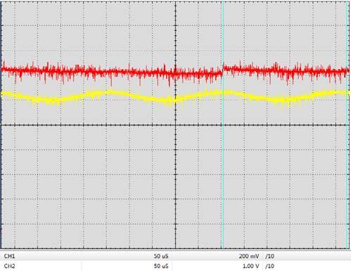
5 The output current formula is: Peak current I OUT (A) = 3.2 V LISH (V) Valley current I OUT (A) = 3.2 V LISL (V) 2.5VR pin can be used as a 2.5V power supply, the maximum output current is 20mA. pin or pin indicates the output current: Output current (A) = 3.2 V (V) represents the instant laser current, while is the peak current. When the modulation speed exceeds 3kHz, will not have the function of indication. Figure 6 is the mathematic model of the s waveform. It s an exponential function, and see the practical waveform in Figure 10. Figure 7. Digital Modulation Response at Pin Figure 6. s Mathematic Model Attenuation speed formula of s waveform is: t 100ms V ( t) = VAe V A is the peak voltage of V. Peak output current (A) = 3.2 V (V) Digital Modulation Response Waveforms When the input PCN is a 100Hz digital signals, the response waveform measured at pin is shown in Figure 7 and the rise and fall time is approximately 56μS. The waveform changes from 0.8V to 1.8V and scanning speed is 50μs/D. Figure 8 shows the same waveform with slower scanning speed: 2ms/D. When the input PCN is a 5kHz digital signal, measured output at pin is shown in Figure 9, the voltage changes from 0.78V to 1.89V and scanning speed is 50μs/D. Figure 8. Digital Modulation Response at Pin Figure 9. Digital Modulation Response at Pin Copyrights , Analog Technologies, Inc. All Rights Reserved. Updated on 9/6/

 Figure 14. 1kHz) Figure 12.")
 Copyrights 2000-2017, Analog")

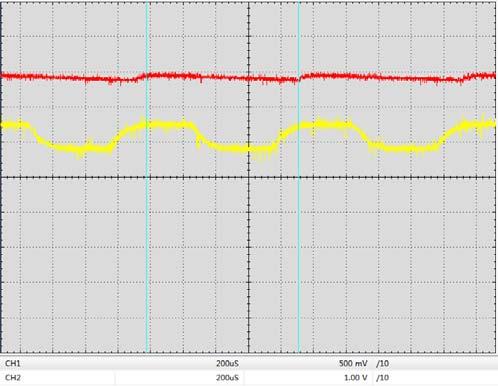
6 Figure 10. Digital Modulation Response at & Pin (f = 100Hz) Figure 13. Digital Modulation Response at & Pin (f = 500Hz) Figure 11. Digital Modulation Response at & Pin (f = 100Hz) Figure 14. Digital Modulation Response at & Pin (f = 1kHz) Figure 12. Digital Modulation Response at & Pin (f = 500Hz) Figure 15. Digital Modulation Response at & Pin (f = 1kHz) Copyrights , Analog Technologies, Inc. All Rights Reserved. Updated on 9/6/

 Figure 20. 4kHz) Figure 18.")
 Copyrights 2000-2017, Analog")

7 Figure 16. Digital Modulation Response at & Pin (f = 2kHz) Figure 19. Digital Modulation Response at & Pin (f = 3kHz) Figure 17. Digital Modulation Response at & Pin (f = 2kHz) Figure 20. Digital Modulation Response at & Pin (f = 4kHz) Figure 18. Digital Modulation Response at & Pin (f = 3kHz) Figure 21. Digital Modulation Response at & Pin (f = 4kHz) Copyrights , Analog Technologies, Inc. All Rights Reserved. Updated on 9/6/
 = 40 0.01082 The V TEMPO is the voltage of TEMPO pin.")
 Load (%) Figure 24. Digital Modulation Response at & Pin (f = 6kHz) Figure 26.")


8 Figure 22. Digital Modulation Response at & Pin (f = 5kHz) Figure 25. Digital Modulation Response at & Pin (f = 6kHz) C. Internal Temperature The module s temperature equation is: VTEMPO Temperatur e( C) = The V TEMPO is the voltage of TEMPO pin. When the TEMPO voltage varies from V to V, the temperature indicated is from 40 C to 140 C. Figure 23. Digital Modulation Response at & Pin (f = 5kHz) Load (%) Figure 24. Digital Modulation Response at & Pin (f = 6kHz) Figure 26. Derating Curve The enable control pin, EN, is used for enabling the power supply. The logic threshold voltage is about 1.2V. When this pin is pulled down to <0.5V, the laser driver is disabled. There is a 100k pull-up resistor tide to a 5V power supply internally. Leaving this pin unconnected or driving it to above the 1.2V threshold voltage will enable the laser driver. The LPGD pin indicates the laser drivers works properly under constant current mode when this pin is pulled high. It can be used for driving an LED directly and the maximum Copyrights , Analog Technologies, Inc. All Rights Reserved. Updated on 9/6/


9 output current is 5mA. D. Testing Results a. Start-up Waveform Figure 27. shows the start-up waveform at the pin. The voltage changes from 0V to 3V without over-shoot and the scanning speed is 50ms/D. Figure 27. Start-up Waveform at Pin b. Ripple voltage Ripple voltage on the pin is 6mV when the output current is 5A, see Figure 28. E. Cautions a. Make sure the ground wire of the AC power plug is connected to the ground. b. Use anti-static measures, such as wrist straps, when handing the module so as not to damage the internal circuits. c. Always connect the module s AC input with a proper cable and a plug, do not use stripped wires as the plug for connecting to the AC main socket. Make sure that the cable wires are firmly tighten by screws onto the terminals to have reliable connections. d. When making modifications on the connections, always turn off the power first. e. Make sure that the polarity of the laser diode matches the polarity of the power supply s output. f. Carefully and patiently check the application circuit. After making sure that all the connections are correct, turn on the power supply. When the Loop Good LED light is lit up, it indicates that control loop is stable and working properly. g. To be on the safe side, we recommend using a dummy laser diode to replace the real laser diode first. The dummy diode can be consisted of a serial of 2 to 3 regular high current diodes, such as 8A to 80A, make sure that enough heat sinking is provided to the diodes, or simply immerse the diodes into a cup of water. Use oscilloscope to look at the output waveform at pin for checking the soft-start and soft-cut circuit. The output current can be measured by measuring the voltage, or to measure the output current directly, use a low resistance current sense resistor inserted into the dummy laser circuit and measure the voltage across the current sense resistor. Figure 28. Noise Waveform at Pin Copyrights , Analog Technologies, Inc. All Rights Reserved. Updated on 9/6/
10 MECHANICAL DIMENSIONS NAMING A AS 8A 19V 2 Figure 29. Mechanical Dimensions Version: the second version Maximum output voltage: 19V Maximum output current: 8A Circuit type: AC input/output isolated Company code: Analog Technologies, Inc. ORDERING INFORMATION TABLE 4. UNIT PRICE Quantity (pcs) $320 $290 $250 $220 $190 $180 Copyrights , Analog Technologies, Inc. All Rights Reserved. Updated on 9/6/
11 NOTICE 1. ATI warrants performance of its products for one year to the specifications applicable at the time of sale, except for those being damaged by excessive abuse. Products found not meeting the specifications within one year from the date of sale can be exchanged free of charge. 2. ATI reserves the right to make changes to its products or to discontinue any product or service without notice, and advise customers to obtain the latest version of relevant information to verify, before placing orders, that information being relied on is current and complete. 3. All products are sold subject to the terms and conditions of sale supplied at the time of order acknowledgment, including those pertaining to warranty, patent infringement, and limitation of liability. Testing and other quality control techniques are utilized to the extent ATI deems necessary to support this warranty. Specific testing of all parameters of each device is not necessarily performed, except those mandated by government requirements. 4. Customers are responsible for their applications using ATI components. In order to minimize risks associated with the customers applications, adequate design and operating safeguards must be provided by the customers to minimize inherent or procedural hazards. ATI assumes no liability for applications assistance or customer product design. 5. ATI does not warrant or represent that any license, either express or implied, is granted under any patent right, copyright, mask work right, or other intellectual property right of ATI covering or relating to any combination, machine, or process in which such products or services might be or are used. ATI s publication of information regarding any third party s products or services does not constitute ATI s approval, warranty or endorsement there of. 6. IP (Intellectual Property) Ownership: ATI retains the ownership of full rights for special technologies and/or techniques embedded in its products, the designs for mechanics, optics, plus all modifications, improvements, and inventions made by ATI for its products and/or projects. Copyrights , Analog Technologies, Inc. All Rights Reserved. Updated on 9/6/
High Efficiency AC Input 12A 12V Laser Driver
 Figure. Front View of the Figure 2. Top View of the FEATURES High efficiency: 70 % Maximum output current: 2A Wide output voltage: 0V ~ 2V Wide input voltage: 00VAC ~ 240VAC High speed digital modulation:
Analog Technologies. Low Noise Constant Current Laser Driver ATLS1A102
 ATLSA0 FEATURES Ultra Low Noise:
Analog Technologies. Dual Mode Laser Driver LDA1-CP1-D
 FEATURES High Efficiency: 90% Maximum Output Current: 2A No Heat Sink Required Current and Power Programming, Modulation & Monitoring Capabilities. Current Output Noise: 0.05% High Stability: 100ppm/ C
Pin # Pin Name Pin Type Description
 Figure 1. Physical Photo of FEATURES Ultra-Low Noise (RMS):
Pin # Pin Name Pin Type Description. 4 GND Signal ground Signal ground pin. Connect ADC and DAC grounds to here.
 FEATURES High Efficiency: 90% Maximum Output Current: 2A No Heat Sink Required Current and Power Programming, Modulation & Monitoring Capabilities. Current Output Noise: 0.05% High Stability: 100ppm/ C
Analog Technologies. High Voltage Constant Current 1A Laser Driver ATLS1A212 DESCRIPTION FEATURES APPLICATIONS
 FEATURES Analog Technologies Figure 1. Physical Photo of D Wide Input Voltage Range: 4.5V 15V Wide Output Voltage Range: 0.8V to 0.9V VPS (input voltage) Maximum Output Current: 1A High Efficiency: 90%
2352 Walsh Ave. Santa Clara, CA U. S. A. Tel.: (408) , Fax: (408)
 , Fax: (408)") FEATURES Analog Technologies High Efficiency: 90% Maximum Output Current: 2A No Heat Sink Required Current and Power Programming, Modulation & Monitoring Capabilities. Current Output Noise: 0.05% High
FEATURES Analog Technologies High Efficiency: 90% Maximum Output Current: 2A No Heat Sink Required Current and Power Programming, Modulation & Monitoring Capabilities. Current Output Noise: 0.05% High
1161 Ringwood Ct, #110, San Jose, CA 95131, U. S. A. Tel.: (408) , Fax: (408)
 , Fax: (408)") Figure 1. Physical Photo of D FEATURES Wide Input Voltage Range: 5.5V 27V Wide Output Voltage Range: 0.1V VPS to 0.8V VPS (input voltage) High Current Capability: 10A High Efficiency: 90% (I OUT =10A@V
Figure 1. Physical Photo of D FEATURES Wide Input Voltage Range: 5.5V 27V Wide Output Voltage Range: 0.1V VPS to 0.8V VPS (input voltage) High Current Capability: 10A High Efficiency: 90% (I OUT =10A@V
Pin # Pin Name Pin Type Description
 Technologies FEATURES High Efficiency: 90% Maximum Output Current: 2A No Heat Sink Required Current and Power Programming, Modulation & Monitoring Capabilities. Current Output Noise: 0.05% High Stability:
Analog Technologies. Noise Measurement Amplifier ATNMA2 Noise Measurement Amplifier
 MAIN FEATURES Built-in rechargeable battery Magnifications: 300, 3,000, 30,000, 300,000, 3,000,000 Three filter bandwidths: 0.1Hz ~ 10Hz, 0.1Hz ~ 1kHz, 0.1Hz ~ 100kHz LED low battery indicator function
Analog Technologies. High Voltage Constant Current 3A Laser Driver ATLS3A212 DESCRIPTION
 Figure 1. Physical Photo of FEATURES Power Supply Voltage VPS Range: 4.5V 16V Full Swing Output Voltage: 0.8V to VPS (input voltage) Maximum Output Current: 3A High Efficiency: 90% - no heat sink is needed
2352 Walsh Ave. Santa Clara, CA U. S. A. Tel.: (408) , Fax: (408)
 , Fax: (408)") FEATURES Figure 1. Physical Photo of D Power Supply Voltage VPS Range: 4.5V ~ 16V Full Swing Output Voltage: 0V to VPS (input voltage) Maximum Output Current: 2A High Efficiency: 92% - no heat sink is
FEATURES Figure 1. Physical Photo of D Power Supply Voltage VPS Range: 4.5V ~ 16V Full Swing Output Voltage: 0V to VPS (input voltage) Maximum Output Current: 2A High Efficiency: 92% - no heat sink is
Analog Technologies. High Efficiency 2.5A TEC Controller. TECA1-xV-xV-D
 temperature measurement network also uses this voltage as the reference, the errors in setting the temperature and measuring the temperature cancel with each other, setting the object temperature with
Analog Technologies ATEC24V10A-D. High Voltage High Current TEC Controller
 FEATURES High Output Voltage: V High Output Current: 0A High Efficiency: >% High Temperature Stability: ±0.0 C Programmable Current Limit Complete Shielding 00 % Lead (Pb)-free and RoHS Compliant Compact
Pin # Pin Name Pin Type Description
 Figure. Physical Photo of S FEATURES Ultra Low Noise:
Analog Technologies. High Efficiency TEC Controller TEC5V4A-D
 Figure 1. Physical photo of FEATURES High Efficiency: 90% Maximum Output Current: 4A Maximum Output Voltage: V VPS 0.2V Actual Object Temperature Monitoring High Stability: 0.01 C High Precision High Reliability
Analog Technologies. High Efficiency 2.5A TEC Controller TECA1-XV-XV-D
 Figure 1. The Photos of Actual FEATURES High Efficiency: 90% Maximum Output Current: 2.5A Actual Object Temperature Monitoring High Stability: 0.01 C High Reliability and Zero EMI Compact Size 100 % lead
Pin # Pin Name Pin Type Description. Shut down control. Negative logic.
 Figure Physical Photo of ATLSA0 FEATURES Ultra Low Noise:
Pin # Pin Name Pin Type Description
 Figure. Physical Photo of D FEATURES Ultra Low Noise:
Analog Technologies. High Efficiency TEC Controller TEC5V6A-D
 Figure 1. Physical photo of FEATURES High Efficiency: 90% Maximum Output Current: 6A Maximum Output Voltage: VPS 0.V Actual Object Temperature Monitoring High Stability: 0.01 C High Reliability Zero EMI
Analog Technologies. High Efficiency 2.5A TEC Controller TECA1-XV-XV-D
 (Potentiometer) or a DAC (Digital to Analog Converter). When using this reference for setting the set-point temperature, the set-point temperature error is independent of this reference voltage. This is
Analog Technologies ATLS100MA104. Low Noise Constant Current Laser Controller
 Figure. Physical Photo of ATLS00mA04 FEATURES Ultra Low Noise (RMS):
Analog Technologies. Auto Iron ATAS80
 Figure 1. The Photo of main machine Figure 2. Photo of MAIN FEATURES Large LCD screen display, convenient for adjusting Anti-static function to protect precise chip soldering Quick temperature rise Unit
2 GND Signal ground Signal ground pin. Connect ADC and DAC grounds to here.
 Figure. Physical Photo of S FEATURES Ultra Low Noise:.5µA P-P @ 0.Hz to 0Hz High Current without Heat Sink: 00mA High Absolute Accuracy:
Pin # Pin Name Pin Type Description
 Figure. Physical Photo of FEATURES Ultra Low Noise: 4.5μA P-P @ 0.Hz to 0Hz High I OUT without Heat Sink: 50mA High I OUT Absolute Accuracy:
Analog Technologies. Low Noise Constant Current Laser Controller ATLS500MA103
 Figure. Physical Photo of S FEATURES Ultra Low Noise: 5µA P-P @ 0.Hz to 0Hz High Current without Heat Sink: 500mA High Absolute Accuracy:
2352 Walsh Ave. Santa Clara, CA U. S. A. Tel.: (408) , Fax: (408)
 , Fax: (408)") FEATURES High Input Voltage: up to 8 V Five Times Longer Battery Run Time than Using an Incandescent Bulb High Luminous Flux: > 90 lumens High Immunity to RF Interference High Efficiency: 92% Long Lasting:
FEATURES High Input Voltage: up to 8 V Five Times Longer Battery Run Time than Using an Incandescent Bulb High Luminous Flux: > 90 lumens High Immunity to RF Interference High Efficiency: 92% Long Lasting:
TEC Controller Evaluation Board TECEV104
 TECEV0 TEC Controller Evaluation Board TECEV0 By Gang Liu BOARD DESCRIPTION The TEC controller evaluation board TECEV0 is consisted of a complete tuning and application circuit for driving a TEC. It can
Figure 1. Physical Photo of AHV24VN3KV1MAW DESCRIPTION
 Figure 1. Physical Photo of FEATURES High precision Full modulation range on output voltage Negative voltage output Linear regulation Shutdown APPLICATIONS This power module,, is designed for achieving
Pin # Pin Name Pin Type Description
 Figure 1. Physical Photo of FEATURES Ultra-Low Noise (RMS):
2 GND Signal ground Signal ground pin. Connect ADC and DAC grounds to here.
 Figure. Physical Photo of S FEATURES Ultra Low Noise: 6µA P-P @0.Hz to 0Hz High Output Current: A High Absolute Accuracy: ± 0.% High Stability:
Figure 1. Physical Photo of AHV12V10KV1MAW
 Figure 1. Physical Photo of FEATURES High precision Full modulation range on output voltage Linear regulation Shutdown APPLICATIONS This power module,, is designed for achieving DC-DC conversion from low
Figure 1. Physical Photo of AHV12VN10KV1MAW
 Figure 1. Physical Photo of FEATURES High precision Full modulation range on output voltage Negative voltage output Linear regulation Shutdown APPLICATIONS This power module,, is designed for achieving
Analog Technologies. ATI2202 Step-Down DC/DC Converter ATI2202. Fixed Frequency: 340 khz
 Step-Down DC/DC Converter Fixed Frequency: 340 khz APPLICATIONS LED Drive Low Noise Voltage Source/ Current Source Distributed Power Systems Networking Systems FPGA, DSP, ASIC Power Supplies Notebook Computers
 IMPORTANT NOTICE Texas Instruments (TI) reserves the right to make changes to its products or to discontinue any semiconductor product or service without notice, and advises its customers to obtain the
Pin-Out Information Pin Function. Inhibit (30V max) Pkg Style 200
 Pkg Style 200") PT6 Series Amp Adjustable Positive Step-down Integrated Switching Regulator SLTS29A (Revised 6/3/2) 9% Efficiency Adjustable Output Voltage Internal Short Circuit Protection Over-Temperature Protection
PT6 Series Amp Adjustable Positive Step-down Integrated Switching Regulator SLTS29A (Revised 6/3/2) 9% Efficiency Adjustable Output Voltage Internal Short Circuit Protection Over-Temperature Protection
Analog Technologies. High Efficiency Window TEC Controller ATW3A313
 Figure 1. Physical Photo of the D FEATURES The world s first window based TEC controller: stands by when the target object temperature is within a pre-set temperature window. Programmable set-point temperature
The PT6300 Series is a line of High-Performance 3 Amp, 12-Pin SIP (Single In-line Package) Integrated. Pin-Out Information Pin Function
 Integrated. Pin-Out Information Pin Function") PT6 Series Amp Adjustable Positive Step-down Integrated Sw itching Regulators SLTSB (Revised 9//) 9% Efficiency Adjustable Output Voltage Internal Short Circuit Protection Over-Temperature Protection On/Off
PT6 Series Amp Adjustable Positive Step-down Integrated Sw itching Regulators SLTSB (Revised 9//) 9% Efficiency Adjustable Output Voltage Internal Short Circuit Protection Over-Temperature Protection On/Off
ULN2804A DARLINGTON TRANSISTOR ARRAY
 HIGH-VOLTAGE, HIGH-CURRENT 500-mA-Rated Collector Current (Single ) High-Voltage s...50 V Clamp Diodes Inputs Compatible With Various Types of Logic Relay Driver Applications Compatible With ULN2800A-Series
TL494M PULSE-WIDTH-MODULATION CONTROL CIRCUIT
 Complete PWM Power Control Circuitry Uncommitted Outputs for 00-mA Sink or Source Current Output Control Selects Single-Ended or Push-Pull Operation Internal Circuitry Prohibits Double Pulse at Either
Current Mode PWM Controller
 Current Mode PWM Controller UC1842/3/4/5 FEATURES Optimized For Off-line And DC To DC Converters Low Start Up Current (
Analog Technologies TEC28V15A. High Voltage High Current TEC Controller
 FEATURES Analog Technologies Figure 1. Physical Photo of Figure 2. Physical Photo of Built-in Smart Auto PID Control the World s First High Output Voltage: 28V High Output Current: 15A High Efficiency:
Analog Technologies VC99. Multimeter FEATURES
 FEATURES LCD Display Max Display: 6000(3 6/7) Digits Automatic Polarity, Unit Symbol and 61 Section Analog Display Measurement Method: Double Integral A/D Conversion Sampling Rate: Approx.3 times/sec Over-Range
Advanced Regulating Pulse Width Modulators
 Advanced Regulating Pulse Width Modulators FEATURES Complete PWM Power Control Circuitry Uncommitted Outputs for Single-ended or Push-pull Applications Low Standby Current 8mA Typical Interchangeable with
TL594 PULSE-WIDTH-MODULATION CONTROL CIRCUITS
 Complete PWM Power Control Circuitry Uncommitted Outputs for 200-mA Sink or Source Current Output Control Selects Single-Ended or Push-Pull Operation Internal Circuitry Prohibits Double Pulse at Either
MC3487 QUADRUPLE DIFFERENTIAL LINE DRIVER
 Meets or Exceeds Requirements of ANSI EIA/TIA-422-B and ITU Recommendation V. -State, TTL-Compatible s Fast Transition Times High-Impedance Inputs Single -V Supply Power-Up and Power-Down Protection Designed
Analog Technologies Inc.
 Analog Technologies Inc. Figure. Physical Photo of the ATWA4D FEATURES The world s first window based TEC controller: stands by automatically when the target object temperature is within a pre-set temperature
MOC3009 THRU MOC3012 OPTOCOUPLERS/OPTOISOLATORS
 5 V Phototriac Driver Output Gallium-Arsenide-Diode Infrared Source and Optically Coupled Silicon Traic Driver (Bilateral Switch) UL Recognized...File Number E585 High Isolation...75 V Peak Output Driver
Stepper Motor Drive Circuit
 Stepper Motor Drive Circuit FEATURES Full-Step, Half-Step and Micro-Step Capability Bipolar Output Current up to 1A Wide Range of Motor Supply Voltage 10-46V Low Saturation Voltage with Integrated Bootstrap
Voltage-to-Frequency and Frequency-to-Voltage CONVERTER
 Voltage-to-Frequency and Frequency-to-Voltage CONVERTER FEATURES OPERATION UP TO 500kHz EXCELLENT LINEARITY ±0.0% max at 0kHz FS ±0.05% max at 00kHz FS V/F OR F/V CONVERSION MONOTONIC VOLTAGE OR CURRENT
TL780 SERIES POSITIVE-VOLTAGE REGULATORS
 ±1% Output Tolerance at ±2% Output Tolerance Over Full Operating Range Thermal Shutdown description Internal Short-Circuit Current Limiting Pinout Identical to µa7800 Series Improved Version of µa7800
Advanced Regulating Pulse Width Modulators
 Advanced Regulating Pulse Width Modulators FEATURES Complete PWM Power Control Circuitry Uncommitted Outputs for Single-ended or Push-pull Applications Low Standby Current 8mA Typical Interchangeable with
High Speed PWM Controller
 High Speed PWM Controller FEATURES Compatible with Voltage or Current Mode Topologies Practical Operation Switching Frequencies to 1MHz 50ns Propagation Delay to Output High Current Dual Totem Pole Outputs
MOC3020 THRU MOC3023 OPTOCOUPLERS/OPTOISOLATORS
 MOC300 THRU MOC303 SOES05A OCTOBER 98 REVISED APRIL 998 00 V Phototriac Driver Output Gallium-Arsenide-Diode Infrared Source and Optically-Coupled Silicon Traic Driver (Bilateral Switch) UL Recognized...
Regulating Pulse Width Modulators
 Regulating Pulse Width Modulators UC1525A/27A FEATURES 8 to 35V Operation 5.1V Reference Trimmed to ±1% 100Hz to 500kHz Oscillator Range Separate Oscillator Sync Terminal Adjustable Deadtime Control Internal
Vout Adjust V OUT LOAD GND
 PT6705 Series 13 Amp 5V/3.3V Input Adjustable Integrated Switching Regulator New Space-Saving Package 3.3V/5V input (12V Bias) Adjustable Output Voltage 90% Efficiency Differential Remote Sense 17-pin
ua9637ac DUAL DIFFERENTIAL LINE RECEIVER
 ua967ac Meets or Exceeds the Requirements of ANSI Standards EIA/TIA--B and EIA/TIA--B and ITU Recommendations V. and V. Operates From Single -V Power Supply Wide Common-Mode Voltage Range High Input Impedance
SN75C1406 TRIPLE LOW-POWER DRIVERS/RECEIVERS
 Meet or Exceed the Requirements of TIA/EIA-232-F and ITU Recommendation V.28 Very Low Power Consumption... 5 mw Typ Wide Driver Supply Voltage Range... ±4.5 V to ±15 V Driver Output Slew Rate Limited to
Isolated High Side FET Driver
 UC1725 Isolated High Side FET Driver FEATURES Receives Both Power and Signal Across the Isolation Boundary 9 to 15 Volt High Level Gate Drive Under-voltage Lockout Programmable Over-current Shutdown and
SN75150 DUAL LINE DRIVER
 Meets or Exceeds the Requirement of TIA/EIA-232-F and ITU Recommendation V.28 Withstands Sustained Output Short Circuit to Any Low-Impedance Voltage Between 25 V and 25 V 2-µs Maximum Transition Time Through
Current Mode PWM Controller
 application INFO available UC1842/3/4/5 Current Mode PWM Controller FEATURES Optimized For Off-line And DC To DC Converters Low Start Up Current (
SN5407, SN5417, SN7407, SN7417 HEX BUFFERS/DRIVERS WITH OPEN-COLLECTOR HIGH-VOLTAGE OUTPUTS
 Converts TTL Voltage Levels to MOS Levels High Sink-Current Capability Clamping Diodes Simplify System Design Open-Collector Driver for Indicator Lamps and Relays s Fully Compatible With Most TTL Circuits
ULN2001A, ULN2002A, ULN2003A, ULN2004A DARLINGTON TRANSISTOR ARRAYS
 ULNA, ULNA, ULNA, ULNA SLRS DECEMBER REVISED APRIL HIGH-VOLTAGE HIGH-CURRENT -ma Rated Collector Current (Single ) High-Voltage s... V Clamp Diodes Inputs Compatible With Various Types of Logic Relay Driver
ICN2053. (16-Channel PWM Constant Current LED Sink Driver)
") ICN2053 (16-Channel PWM ) Description The ICN2053 is a 16-channel PWM constant current sink output LED driver for 1:32 time multiplexing applications. The constant-current value of all 16 channels is set
ICN2053 (16-Channel PWM ) Description The ICN2053 is a 16-channel PWM constant current sink output LED driver for 1:32 time multiplexing applications. The constant-current value of all 16 channels is set
SN75468, SN75469 DARLINGTON TRANSISTOR ARRAYS
 SLRSB DECEMBER REVISED SEPTEMBER HIGH-VOLTAGE HIGH-CURRENT -ma Rated Collector Current (Single ) High-Voltage s... V Clamp Diodes Inputs Compatible With Various Types of Logic Relay Driver Applications
SN55451B, SN55452B, SN55453B, SN55454B SN75451B, SN75452B, SN75453B, SN75454B DUAL PERIPHERAL DRIVERS
 PERIPHERAL DRIVERS FOR HIGH-CURRENT SWITCHING AT VERY HIGH SPEEDS Characterized for Use to 00 ma High-Voltage Outputs No Output Latch-Up at 0 V (After Conducting 00 ma) High-Speed Switching Circuit Flexibility
TL594 PULSE-WIDTH-MODULATION CONTROL CIRCUIT
 Complete PWM Power Control Circuitry Uncommitted Outputs for 200-mA Sink or Source Current Output Control Selects Single-Ended or Push-Pull Operation Internal Circuitry Prohibits Double Pulse at Either
NE5532, NE5532A DUAL LOW-NOISE OPERATIONAL AMPLIFIERS
 Equivalent Input Noise Voltage 5 nv/ Hz Typ at 1 khz Unity-Gain Bandwidth... 10 MHz Typ Common-Mode Rejection Ratio... 100 db Typ High dc Voltage Gain... 100 V/mV Typ Peak-to-Peak Output Voltage Swing
Resonant-Mode Power Supply Controllers
 Resonant-Mode Power Supply Controllers UC1861-1868 FEATURES Controls Zero Current Switched (ZCS) or Zero Voltage Switched (ZVS) Quasi-Resonant Converters Zero-Crossing Terminated One-Shot Timer Precision
SN75158 DUAL DIFFERENTIAL LINE DRIVER
 SN78 Meets or Exceeds the Requirements of ANSI EIA/TIA--B and ITU Recommendation V. Single -V Supply Balanced-Line Operation TTL Compatible High Output Impedance in Power-Off Condition High-Current Active-Pullup
TL1431 PRECISION PROGRAMMABLE REFERENCE
 PRECISION PROGRAMMABLE REFEREE 0.4% Initial Voltage Tolerance 0.2-Ω Typical Output Impedance Fast Turnon... 500 ns Sink Current Capability...1 ma to 100 ma Low Reference Current (REF) Adjustable Output
Analog Technologies. Multimeter DM4070
 Figure 1. The Photo of Actual FEATURES LCD Display Over Range: Display 1 Inductance Measure: 0.1uH-20H Capacitance Measure: 0.1pF-2000uF Resistance Measure: 0.01Ω-20MΩ Low Battery Indication: Symbol Display
TL FIXED-VOLTAGE REGULATORS FOR SCSI ACTIVE TERMINATION
 Fully Matches Parameters for SCSI Alternative 2 Active Termination Fixed 2.85-V Output ±1.5% Maximum Output Tolerance at T J = 25 C 1-V Maximum Dropout Voltage 500-mA Output Current ±3% Absolute Output
TL431, TL431A ADJUSTABLE PRECISION SHUNT REGULATORS
 Equivalent Full-Range Temperature Coefficient... 0 ppm/ C 0.-Ω Typical Output Impedance Sink-Current Capability...1 ma to 100 ma Low Output Noise Adjustable Output Voltage...V ref to 6 V Available in a
SN55115, SN75115 DUAL DIFFERENTIAL RECEIVERS
 SN, SN7 Choice of Open-Collector or Active Pullup (Totem-Pole) Outputs Single -V Supply Differential Line Operation Dual-Channel Operation TTL Compatible ± -V Common-Mode Input Voltage Range Optional-Use
SN QUADRUPLE HALF-H DRIVER
 -A -Current Capability Per Driver Applications Include Half-H and Full-H Solenoid Drivers and Motor Drivers Designed for Positive-Supply Applications Wide Supply-Voltage Range of 4.5 V to 6 V TTL- and
TL-SCSI285 FIXED-VOLTAGE REGULATORS FOR SCSI ACTIVE TERMINATION
 Fully Matches Parameters for SCSI Alternative 2 Active Termination Fixed 2.85-V Output ±1% Maximum Output Tolerance at T J = 25 C 0.7-V Maximum Dropout Voltage 620-mA Output Current ±2% Absolute Output
TIL300, TIL300A PRECISION LINEAR OPTOCOUPLER
 ac or dc Signal Coupling Wide Bandwidth...>200 khz High Transfer-Gain Stability...±0.0%/ C 00 V Peak Isolation UL Approval Pending Applications Power-Supply Feedback Medical-Sensor Isolation Opto Direct-Access
TL431, TL431A ADJUSTABLE PRECISION SHUNT REGULATORS
 Equivalent Full-Range Temperature Coefficient... 30 ppm/ C 0.2-Ω Typical Output Impedance Sink-Current Capability...1 ma to 100 ma Low Output Noise Adjustable Output Voltage...V ref to 36 V Available in
TPS7415, TPS7418, TPS7425, TPS7430, TPS7433 FAST-TRANSIENT-RESPONSE USING SMALL OUTPUT CAPACITOR 200-mA LOW-DROPOUT VOLTAGE REGULATORS
 Fast Transient Response Using Small Output Capacitor ( µf) 2-mA Low-Dropout Voltage Regulator Available in.5-v,.8-v, 2.5-V, 3-V and 3.3-V Dropout Voltage Down to 7 mv at 2 ma () 3% Tolerance Over Specified
Current Mode PWM Controller
 Current Mode PWM Controller FEATURES Automatic Feed Forward Compensation Programmable Pulse-by-Pulse Current Limiting Automatic Symmetry Correction in Push-pull Configuration Enhanced Load Response Characteristics
Description The PT8000 series is a 60 A highperformance,
 PT8000 5V 60 Amp High-Performance Programmable ISR SLTS135A (Revised 4/5/2001) Features 60A Output Current Multi-Phase Topology +5V Input 5-bit Programmable: 1.3V to 3.5V 1.075V to 1.850V High Efficiency
Ordering Information PT5521 =3.3 Volts PT5522 =2.5 Volts PT5523 =2.0 Volts PT5524 =1.8 Volts PT5525 =1.5 Volts PT5526 =1.2 Volts PT5527 =1.
 PT552 Series 1.5-A 5-V/3.3-V Input Adjustable Integrated Switching Regulator SLTS147A (Revised 1/5/21) Features Single-Device: 5V/3.3V Input DSP Compatible 89% Efficiency Small Footprint Space-Saving package
SN75C185 LOW-POWER MULTIPLE DRIVERS AND RECEIVERS
 Meets or Exceeds the Requirements of ANSI EIA/TIA-232-E and ITU Recommendation V.28 Single Chip With Easy Interface Between UART and Serial Port Connector Less Than 9-mW Power Consumption Wide Driver Supply
SN75C185 LOW-POWER MULTIPLE DRIVERS AND RECEIVERS
 Meets or Exceeds the Requirements of TIA/EIA-232-F and ITU Recommendation V.28 Single Chip With Easy Interface Between UART and Serial-Port Connector Less Than 9-mW Power Consumption Wide Driver Supply
SN75150 DUAL LINE DRIVER
 Meets or Exceeds the Requirement of ANSI EIA/TIA-232-E and ITU Recommendation V.28 Withstands Sustained Output Short Circuit to Any Low-Impedance Voltage Between 25 V and 25 V 2-µs Max Transition Time
RC4136, RM4136, RV4136 QUAD GENERAL-PURPOSE OPERATIONAL AMPLIFIERS
 Continuous-Short-Circuit Protection Wide Common-Mode and Differential Voltage Ranges No Frequency Compensation Required Low Power Consumption No Latch-Up Unity Gain Bandwidth... MHz Typ Gain and Phase
Switched Mode Controller for DC Motor Drive
 Switched Mode Controller for DC Motor Drive FEATURES Single or Dual Supply Operation ±2.5V to ±20V Input Supply Range ±5% Initial Oscillator Accuracy; ± 10% Over Temperature Pulse-by-Pulse Current Limiting
High-Side Measurement CURRENT SHUNT MONITOR
 INA39 INA69 www.ti.com High-Side Measurement CURRENT SHUNT MONITOR FEATURES COMPLETE UNIPOLAR HIGH-SIDE CURRENT MEASUREMENT CIRCUIT WIDE SUPPLY AND COMMON-MODE RANGE INA39:.7V to 40V INA69:.7V to 60V INDEPENDENT
SN75C1406 TRIPLE LOW-POWER DRIVERS/RECEIVERS
 Meet or Exceed the Requirements of ANSI EIA/TIA-232-E and ITU Recommendation V.28 Very Low Power Consumption 5 mw Typ Wide Driver Supply Voltage Range ±4.5 V to ±15 V Driver Output Slew Rate Limited to
TL594C, TL594I, TL594Y PULSE-WIDTH-MODULATION CONTROL CIRCUITS
 Complete PWM Power Control Circuitry Uncommitted Outputs for 200-mA Sink or Source Current Output Control Selects Single-Ended or Push-Pull Operation Internal Circuitry Prohibits Double Pulse at Either
ORDERING INFORMATION PACKAGE
 Member of Texas Instruments Widebus Family Latch-Up Performance Exceeds 250 ma Per JESD 17 ESD Protection Exceeds JESD 22 2000-V Human-Body Model (A114-A) 200-V Machine Model (A115-A) Bus Hold on Data
TL598 PULSE-WIDTH-MODULATION CONTROL CIRCUITS
 Complete PWM Power Control Function Totem-Pole Outputs for 200-mA Sink or Source Current Output Control Selects Parallel or Push-Pull Operation Internal Circuitry Prohibits Double Pulse at Either Output
TL494C, TL494I, TL494M, TL494Y PULSE-WIDTH-MODULATION CONTROL CIRCUITS
 Complete PWM Power Control Circuitry Uncommitted Outputs for 00-mA Sink or Source Current Output Control Selects Single-Ended or Push-Pull Operation Internal Circuitry Prohibits Double Pulse at Either
Implications of Slow or Floating CMOS Inputs
 Implications of Slow or Floating CMOS Inputs SCBA4 13 1 IMPORTANT NOTICE Texas Instruments (TI) reserves the right to make changes to its products or to discontinue any semiconductor product or service
REI Datasheet. UC494A, UC494AC, UC495A, UC495AC Advanced Regulatin Pulse Width Modulators. Quality Overview
 UC494A, UC494AC, UC495A, UC495AC Advanced Regulatin Pulse Width Modulators REI Datasheet This entire series of PWM modulators each provide a complete pulse width modulation system in a single monolithic
SN75374 QUADRUPLE MOSFET DRIVER
 SLRS28 SEPTEMBER 1988 Quadruple Circuits Capable of Driving High-Capacitance Loads at High Speeds Output Supply Voltage Range From 5 V to 24 V Low Standby Power Dissipation V CC3 Supply Maximizes Output
Current Mode PWM Controller
 Current Mode PWM Controller application INFO available FEATURES Optimized for Off-line and DC to DC Converters Low Start Up Current (
PRECISION VOLTAGE REGULATORS
 SLVS057B AUGUST 1972 RESED AUGUST 1995 150-mA Load Current Without External Power Transistor Typically 0.02% Input Regulation and 0.03% Load Regulation (µa723m) Adjustable Current Limiting Capability Input
SN54HC365, SN74HC365 HEX BUFFERS AND LINE DRIVERS WITH 3-STATE OUTPUTS
 High-Current -State s Drive Bus Lines, Buffer Memory Address Registers, or Drive up to LSTTL Loads True s Package Options Include Plastic Small-Outline (D) and Ceramic Flat (W) Packages, Ceramic Chip Carriers