Semiconductor Foundry Verification
|
|
|
- Russell Hensley
- 6 years ago
- Views:
Transcription


1 Semiconductor Foundry Verification Alexander Volynkin, Ph.D. In collaboration with Sandia, DOJ and CMU/ECE 1
2 Copyright 2016 Carnegie Mellon University This material is based upon work funded and supported by the Department of Defense under Contract No. FA C-0003 with Carnegie Mellon University for the operation of the Software Engineering Institute, a federally funded research and development center. NO WARRANTY. THIS CARNEGIE MELLON UNIVERSITY AND SOFTWARE ENGINEERING INSTITUTE MATERIAL IS FURNISHED ON AN AS-IS BASIS. CARNEGIE MELLON UNIVERSITY MAKES NO WARRANTIES OF ANY KIND, EITHER EXPRESSED OR IMPLIED, AS TO ANY MATTER INCLUDING, BUT NOT LIMITED TO, WARRANTY OF FITNESS FOR PURPOSE OR MERCHANTABILITY, EXCLUSIVITY, OR RESULTS OBTAINED FROM USE OF THE MATERIAL. CARNEGIE MELLON UNIVERSITY DOES NOT MAKE ANY WARRANTY OF ANY KIND WITH RESPECT TO FREEDOM FROM PATENT, TRADEMARK, OR COPYRIGHT INFRINGEMENT. [Distribution Statement A] This material has been approved Please see Copyright notice for non-us Government use and distribution. This material may be reproduced in its entirety, without modification, and freely distributed in written or electronic form without requesting formal permission. Permission is required for any other use. Requests for permission should be directed to the Software Engineering Institute at permission@sei.cmu.edu. Carnegie Mellon is registered in the U.S. Patent and Trademark Office by Carnegie Mellon University. DM
3 Foundation and Collaboration Collaboration: Sandia counterfeit microcontroller detection CMU/ECE Foundry information, samples of various manufacturing processes DOJ Counterfeit microcontroller samples Foundation: Research project based on SEI s previous research related to microcontroller algorithms detection and recovery SEI s extensive experience in code analysis and anomaly detection 3
4 Problem Statement Chips delivered are not the chips requested Different layout, process, materials, components, tolerances, etc. May or may not do everything the original chip does May or may not do extra, potentially undesirable things as well Most chips in consumer devices not made in U.S. Introduces supply chain issues Subcontractor of subcontractor of subcontractor of Chip markings and packaging often similar/identical Need deeper analysis 4
5 Research Objectives Semi-automated image processing to identify semiconductor foundry Each layer is photographed and processed Relevant features extracted and checked against rules Fabrication facilities have design and fabrication requirements and tolerances Some potential examples: No acute angles or angles of non-45 degree integer multiples All metal feature sizes must be multiples of X nm Metal layers will be copper Failure to meet these rules flags chips as potential counterfeits 5
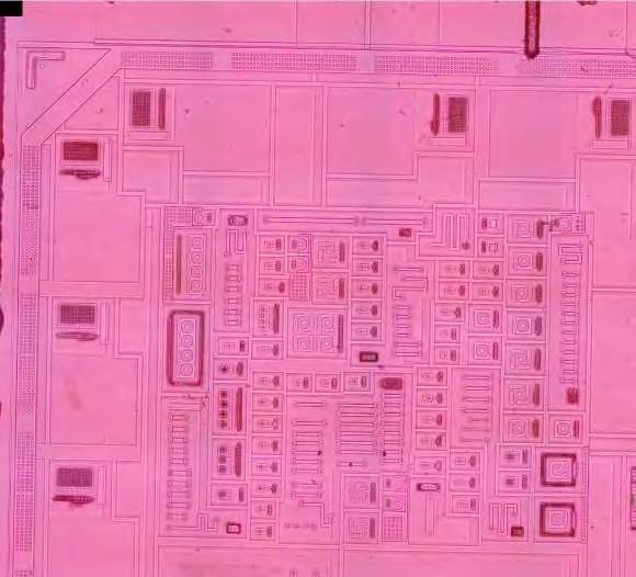
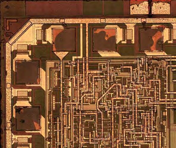
6 Integrated Circuit Fabrication Doping agents, glasses, or metals on silicon Individual components nowadays are on the order of 100nm~10nm Chips are multi-layered Bottom layer is transistors, other silicon features Layers above alternate: - Metal interconnects (copper/aluminum) - Vias (same material as metal) - Glass (Silicon Dioxide) between all of this, isolating the layers Topmost layer contains pads for connecting to packaging and an encapsulation layer 6
7 Integrated Circuit Delayering Chemical processing to strip individual layers off Basically controlled dissolving of glass and metal Primary chemicals: Copper/aluminum etchant (depending on IC metal layer) Hydrofluoric acid (for dissolving glass) Phosphoric acid (for dissolving encapsulation layer) Dissolving each layer requires two or three steps (depending on layer) Layers imaged with optical microscopy camera at each layer 7
")

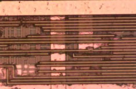
8 Pre-etch, 40x (scaled down resolution) Encapsulation and glass etched, 40x (scaled down resolution) 8

9 Pre-etch, 40x (scaled down resolution) 9

10 Top metal layer removed, 40x (scaled down resolution) 10

11 Counterfeit Examples 11

12 Decapping and Visual Analysis 12


13 Features at Different Layers 13
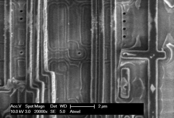
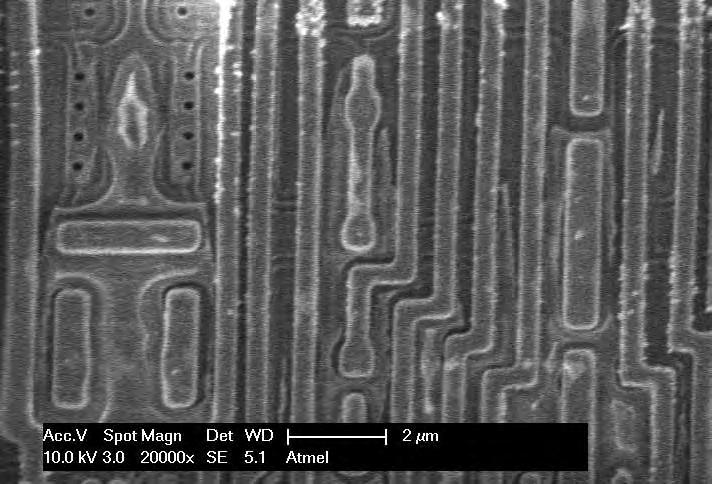
14 Counterfeit Chip at Different Layers 14
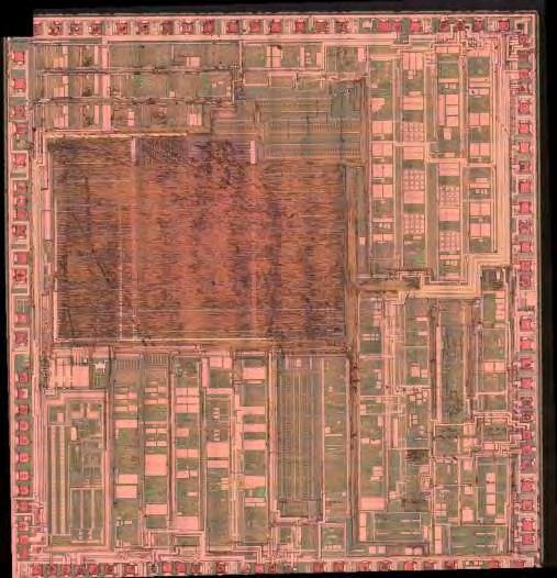
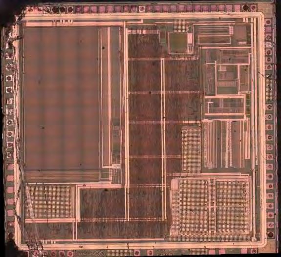
15 Differences in Fabrication 15

16 Same Foundry 16

17 Different Foundries 17

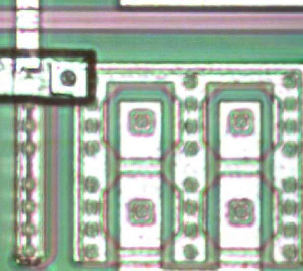
18 Different Foundries 18
19 Other Deliverables: Automated Analysis Methods and Results DBScan_points.py is a program used in FIJI to gather the points in a readable format for other programs that perform cluster analysis. DBScan.py performs the density based spatial cluster analysis with noise. PDBScan_convert.py is a program to convert the point set to another format for a different program to read and perform parallel cluster analysis. SelectPoints.py is a program to take the points of a cluster and select them as multi point selection ROI in FIJI 3D_DBScan_points.py gathers the points in a readable format for the 3D_DBScan.py program. 3D_DBScan.py performs DBScan on RGB coordinates in an image. Color_on_image.py takes the found clusters and colors the image accordingly in FIJI. 19


20 Project Deliverables: Automated Analysis Framework 20
21 Square Area Density Based Spatial Cluster Analysis with Noise (SADBSCAN) Method of cluster analysis specifically designed for segmentation and area differentiation in images Weights the geographical difference as more important and mark these objects as different clusters Queries different regions separately and efficiently Calculates simple Euclidian distance of color values Combines clusters of pixels based not only on color similarities but also the geographic location Result: Accurate feature detection with high speed parallel processing (10-15 minutes on 1GB image) 21

22 Counterfeit Differences Circular features, non-45- degree angles Aluminum, instead of copper 22

23 Next Steps 23

24 Next Steps 24
Guided Architecture Trade Space Exploration of Safety Critical Software Systems
 Guided Architecture Trade Space Exploration of Safety Critical Software Systems Sam Procter, Architecture Researcher Copyright 2017 Carnegie Mellon University. All Rights Reserved. This material is based
Carnegie Mellon University Notice
 Carnegie Mellon University Notice This video and all related information and materials ( materials ) are owned by Carnegie Mellon University. These materials are provided on an as-is as available basis
Machine Learning for Big Data Systems Acquisition
 Machine Learning for Big Data Systems Acquisition John Klein Software Engineering Institute Carnegie Mellon University Pittsburgh, PA 15213 Copyright 2015 Carnegie Mellon University This material is based
Technical Debt Analysis through Software Analytics
 Research Review 2017 Technical Debt Analysis through Software Analytics Dr. Ipek Ozkaya Principal Researcher 1 Copyright 2017 Carnegie Mellon University. All Rights Reserved. This material is based upon
Agile Acquisition of Agile C2
 Software Engineering Institute Carnegie Mellon University Pittsburgh, PA 15213 Dr. Paul Nielsen June 20, 2012 Introduction Commanders are increasingly more engaged in day-to-day activities There is a rapid
Measure it? Manage it? Ignore it? Software Practitioners and Technical Debt
 Measure it? Manage it? Ignore it? Software Practitioners and Technical Debt Neil A. Ernst, Stephany Bellomo, Ipek Ozkaya, Robert Nord, Ian Gorton (FSE) Release; Distribution is Unlimited Copyright 2016
Carnegie Mellon University Notice
 1 Carnegie Mellon University Notice This video and all related information and materials ( materials ) are owned by Carnegie Mellon University. These materials are provided on an as-is as available basis
Driving Efficiencies into the Software Life Cycle for Army Systems
 Driving Efficiencies into the Software Life Cycle for Army Systems Stephen Blanchette Jr. Presented to the CECOM Software Solarium Software Engineering Institute Carnegie Mellon University Pittsburgh,
Fall 2014 SEI Research Review Aligning Acquisition Strategy and Software Architecture
 Fall 2014 SEI Research Review Aligning Acquisition Strategy and Software Architecture Software Engineering Institute Carnegie Mellon University Pittsburgh, PA 15213 Brownsword, Place, Albert, Carney October
Analytical Evaluation Framework
 Analytical Evaluation Framework Tim Shimeall CERT/NetSA Group Software Engineering Institute Carnegie Mellon University August 2011 Disclaimer NO WARRANTY THIS MATERIAL OF CARNEGIE MELLON UNIVERSITY AND
A Mashup of Techniques to Create Reference Architectures
 A Mashup of Techniques to Create Reference Architectures Software Engineering Institute Carnegie Mellon University Pittsburgh, PA 15213 Rick Kazman, John McGregor Copyright 2012 Carnegie Mellon University.
Analytical Evaluation Framework
 Analytical Evaluation Framework Tim Shimeall CERT/NetSA Group Software Engineering Institute Carnegie Mellon University August 2011 Report Documentation Page Form Approved OMB No. 0704-0188 Public reporting
The Impact of Conducting ATAM Evaluations on Army Programs
 The Impact of Conducting ATAM Evaluations on Army Programs Software Engineering Institute Carnegie Mellon University Pittsburgh, PA 15213 Robert L. Nord, John Bergey, Stephen Blanchette, Jr., Mark Klein
Multi-Agent Decentralized Planning for Adversarial Robotic Teams
 Multi-Agent Decentralized Planning for Adversarial Robotic Teams James Edmondson David Kyle Jason Blum Christopher Tomaszewski Cormac O Meadhra October 2016 Carnegie 26, 2016Mellon University 1 Copyright
Smart Grid Maturity Model: A Vision for the Future of Smart Grid
 Smart Grid Maturity Model: A Vision for the Future of Smart Grid David W. White Smart Grid Maturity Model Project Manager White is a member of the Resilient Enterprise Management (REM) team in the CERT
Evaluation of Competing Threat Modeling Methodologies
 Evaluation of Competing Threat Modeling Methodologies Dr. Forrest Shull Team: Nancy Mead, Kelwyn Pender, & Sam Weber (SEI) Jane Cleland-Huang, Janine Spears, & Stefan Hiebl (DePaul) Tadayoshi Kohno (University
Discerning the Intent of Maturity Models from Characterizations of Security Posture
 Discerning the Intent of Maturity Models from Characterizations of Security Posture Rich Caralli January 2012 MATURITY MODELS Maturity models in their simplest form are intended to provide a benchmark
Basic Functional Analysis. Sample Report Richmond Road, Suite 500, Ottawa, ON K2H 5B7 Canada Tel:
 Basic Functional Analysis Sample Report 3685 Richmond Road, Suite 500, Ottawa, ON K2H 5B7 Canada Tel: 613-829-0414 www.chipworks.com Basic Functional Analysis Sample Report Some of the information in this
Improving Software Sustainability Through Data-Driven Technical Debt Management
 Improving Software Sustainability Through Data-Driven Technical Debt Management Ipek Ozkaya October 7, 2015 Software Engineering Institute Carnegie Mellon University Pittsburgh, PA 15213 Copyright 2015
Frameworks for Assessing IT Systems Engineering Acquisition Issues and Proposed Approaches in Support of Public Law 111
 Frameworks for Assessing IT Systems Engineering Acquisition Issues and Proposed Approaches in Support of Public Law 111 15 th Annual Systems Engineering Conference Net Centric Operations/Interoperability
OSATE overview & community updates
 OSATE overview & community updates Software Engineering Institute Carnegie Mellon University Pittsburgh, PA 15213 Julien Delange AADL Meeting February 15 2013 Carnegie Mellon University Report Documentation
Aptina MT9P111 5 Megapixel, 1/4 Inch Optical Format, System-on-Chip (SoC) CMOS Image Sensor
 CMOS Image Sensor") Aptina MT9P111 5 Megapixel, 1/4 Inch Optical Format, System-on-Chip (SoC) CMOS Image Sensor Imager Process Review For comments, questions, or more information about this report, or for any additional technical
Aptina MT9P111 5 Megapixel, 1/4 Inch Optical Format, System-on-Chip (SoC) CMOS Image Sensor Imager Process Review For comments, questions, or more information about this report, or for any additional technical
Panasonic DMC-GH Mp, 4.4 µm Pixel Size LiveMOS Image Sensor from Panasonic LUMIX DMC-GH1 Micro Four Thirds Digital Interchangeable Lens Camera
 Panasonic DMC-GH1 12.1 Mp, 4.4 µm Pixel Size LiveMOS Image Sensor from Panasonic LUMIX DMC-GH1 Micro Four Thirds Digital Interchangeable Lens Camera Imager Process Review For comments, questions, or more
Sonion TC100Z21A DigiSiMic Silicon Condensor Microphone MEMS Process Review
 November 8, 2006 Sonion TC100Z21A DigiSiMic Silicon Condensor Microphone MEMS Process Review For comments, questions, or more information about this report, or for any additional technical needs concerning
DoD Joint Federated Assurance Center (JFAC) Industry Outreach
 Industry Outreach") DoD Joint Federated Assurance Center (JFAC) Industry Outreach Thomas D. Hurt Office of the Deputy Assistant Secretary of Defense for Systems Engineering Paul R. Croll Co-Chair, NDIA Software Committee
DoD Joint Federated Assurance Center (JFAC) Industry Outreach Thomas D. Hurt Office of the Deputy Assistant Secretary of Defense for Systems Engineering Paul R. Croll Co-Chair, NDIA Software Committee
Intel Xeon E3-1230V2 CPU Ivy Bridge Tri-Gate 22 nm Process
 Intel Xeon E3-1230V2 CPU Structural Analysis 3685 Richmond Road, Suite 500, Ottawa, ON K2H 5B7 Canada Tel: 613-829-0414 www.chipworks.com Structural Analysis Some of the information in this report may
CMOS Digital Integrated Circuits Lec 2 Fabrication of MOSFETs
 CMOS Digital Integrated Circuits Lec 2 Fabrication of MOSFETs 1 CMOS Digital Integrated Circuits 3 rd Edition Categories of Materials Materials can be categorized into three main groups regarding their
Agilent 2AZ1A CMOS Image Sensor Process Review
 October 13, 2006 Agilent 2AZ1A CMOS Image Sensor Process Review For comments, questions, or more information about this report, or for any additional technical needs concerning semiconductor technology,
Lecture 0: Introduction
 Lecture 0: Introduction Introduction Integrated circuits: many transistors on one chip. Very Large Scale Integration (VLSI): bucketloads! Complementary Metal Oxide Semiconductor Fast, cheap, low power
Toshiba HEK3 0.3 Mp VGA CMOS Image Sensor 0.13 µm Toshiba Process
 Toshiba HEK3 0.3 Mp VGA CMOS Image Sensor 0.13 µm Toshiba Process Through Silicon Via Process Review For comments, questions, or more information about this report, or for any additional technical needs
InvenSense IDG-300 Dual-Axis Angular Rate Gyroscope Sensor
 InvenSense IDG-300 Dual-Axis Angular Rate Gyroscope Sensor MEMS Process Review For comments, questions, or more information about this report, or for any additional technical needs concerning semiconductor
Qualcomm MSM8926 Snapdragon 400 Application Processor
 Qualcomm MSM8926 Snapdragon 400 Basic Functional Analysis 1891 Robertson Road, Suite 500, Ottawa, ON K2H 5B7 Canada Tel: 613-829-0414 www.chipworks.com Basic Functional Analysis 2 Some of the information
Qualcomm QFE1100 Envelope Tracking PA Power Supply
 Qualcomm QFE1100 1891 Robertson Road, Suite 500, Ottawa, ON K2H 5B7 Canada Tel: 613-829-0414 www.chipworks.com Some of the information in this report may be covered by patents, mask and/or copyright protection.
Samsung SDP1301 DTV SERDES Interface
 Samsung SDP1301 Basic Functional Analysis 1891 Robertson Road, Suite 500, Ottawa, ON K2H 5B7 Canada Tel: 613-829-0414 www.chipworks.com Basic Functional Analysis 2 Some of the information in this report
Freescale SCK20DN51Z K20 USB MHz Microcontroller eflash. Flash Process Review
 Freescale SCK20DN51Z K20 USB 2.0 50 MHz Microcontroller eflash Flash Process Review Freescale SCK20DN51Z Microcontroller eflash 2 Some of the information in this report may be covered by patents, mask
Evolution of a Software Engineer in a SoS System Engineering World
 Evolution of a Software Engineer in a SoS System Engineering World Software Engineering Institute Carnegie Mellon University Pittsburgh, PA 15213 Tricia Oberndorf, Carol A. Sledge, PhD April 2010 NO WARRANTY
Integrated diodes. The forward voltage drop only slightly depends on the forward current. ELEKTRONIKOS ĮTAISAI
 1 Integrated diodes pn junctions of transistor structures can be used as integrated diodes. The choice of the junction is limited by the considerations of switching speed and breakdown voltage. The forward
Course Outcome of M.Tech (VLSI Design)
") Course Outcome of M.Tech (VLSI Design) PVL108: Device Physics and Technology The students are able to: 1. Understand the basic physics of semiconductor devices and the basics theory of PN junction. 2.
Course Outcome of M.Tech (VLSI Design) PVL108: Device Physics and Technology The students are able to: 1. Understand the basic physics of semiconductor devices and the basics theory of PN junction. 2.
Apple/Dialog Semiconductor 343S0622-A1/D2018A WLED Driver
 Apple/Dialog Semiconductor 343S0622-A1/D2018A 1891 Robertson Road, Suite 500, Ottawa, ON K2H 5B7 Canada Tel: 613-829-0414 www.chipworks.com Some of the information in this report may be covered by patents,
u-blox M8030-KT Concurrent Multi-GNSS Receiver
 u-blox M8030-KT Basic Functional Analysis 1891 Robertson Road, Suite 500, Ottawa, ON K2H 5B7 Canada Tel: 613-829-0414 www.chipworks.com Basic Functional Analysis 2 Some of the information in this report
Marvell Avastar 88W ac Wi-Fi 2x2 MIMO Combo Chip
 Marvell Avastar 88W8897 Basic Functional Analysis 1891 Robertson Road, Suite 500, Ottawa, ON K2H 5B7 Canada Tel: 613-829-0414 www.chipworks.com Basic Functional Analysis 2 Some of the information in this
DARPA TRUST in IC s Effort. Dr. Dean Collins Deputy Director, MTO 7 March 2007
 DARPA TRUST in IC s Effort Dr. Dean Collins Deputy Director, MTO 7 March 27 Report Documentation Page Form Approved OMB No. 74-88 Public reporting burden for the collection of information is estimated
Texas Instruments BQ29330 Battery Protection AFE from BQ20Z95DBT
 Texas Instruments BQ29330 Battery Protection AFE from BQ20Z95DBT Process Review For comments, questions, or more information about this report, or for any additional technical needs concerning semiconductor
FocalTech Systems FT5336GQQ and FT5436iGQQ (FS-123ATPBC Die) Capacitive Touch Screen Controller
 Capacitive Touch Screen Controller") FocalTech Systems FT5336GQQ and FT5436iGQQ (FS-123ATPBC Die) 1891 Robertson Road, Suite 500, Ottawa, ON K2H 5B7 Canada Tel: 613-829-0414 www.chipworks.com Some of the information in this report may be
FocalTech Systems FT5336GQQ and FT5436iGQQ (FS-123ATPBC Die) 1891 Robertson Road, Suite 500, Ottawa, ON K2H 5B7 Canada Tel: 613-829-0414 www.chipworks.com Some of the information in this report may be
Module 2: CMOS FEOL Analysis
 Module 2: CMOS FEOL Analysis Manufacturer Device # 2 About Chipworks Chipworks is the recognized leader in reverse engineering and patent infringement analysis of semiconductors and electronic systems.
Nikon NC81369R 24.2 Mp, 3.8 µm Pixel Size, APS-C Format CMOS Image Sensor from the Nikon D3200. Module 5: Substrate Dopant Analysis
 Nikon NC81369R 24.2 Mp, 3.8 µm Pixel Size, APS-C Format CMOS Image Sensor from the Nikon D3200 Module 5: Substrate Dopant Analysis Nikon NC81369R CMOS Image Sensor from the Nikon D3200 2 Some of the information
Component Package Decapsulation Process with Analogue Signature Analysis Support
 Component Package Decapsulation Process with Analogue Signature Analysis Support NEUMANN PETR, ADAMEK MILAN, SKOCIK PETR Faculty of Applied Informatics Tomas Bata University in Zlin nam.t.g.masaryka 5555
Photolithography I ( Part 1 )
") 1 Photolithography I ( Part 1 ) Chapter 13 : Semiconductor Manufacturing Technology by M. Quirk & J. Serda Bjørn-Ove Fimland, Department of Electronics and Telecommunication, Norwegian University of Science
1 Photolithography I ( Part 1 ) Chapter 13 : Semiconductor Manufacturing Technology by M. Quirk & J. Serda Bjørn-Ove Fimland, Department of Electronics and Telecommunication, Norwegian University of Science
Applications of Maskless Lithography for the Production of Large Area Substrates Using the SF-100 ELITE. Jay Sasserath, PhD
 Applications of Maskless Lithography for the Production of Large Area Substrates Using the SF-100 ELITE Executive Summary Jay Sasserath, PhD Intelligent Micro Patterning LLC St. Petersburg, Florida Processing
End-of-line Standard Substrates For the Characterization of organic
 FRAUNHOFER INSTITUTe FoR Photonic Microsystems IPMS End-of-line Standard Substrates For the Characterization of organic semiconductor Materials Over the last few years, organic electronics have become
Foveon FX17-78-F13D Mp, 7.8 µm Pixel Size CIS from Sigma DP1 Compact Digital Camera 0.18 µm Dongbu Process
 Foveon FX17-78-F13D-07 14.1 Mp, 7.8 µm Pixel Size CIS from Sigma DP1 Compact Digital Camera 0.18 µm Dongbu Process Imager Process Review For comments, questions, or more information about this report,
Sony IMX118CQT 18.5 Mp, 1.25 µm Pixel Pitch Back Illuminated CIS from the Sony DSC-WX100 Camera
 18.5 Mp, 1.25 µm Pixel Pitch Back Illuminated CIS from the Sony DSC-WX100 Camera Imager Process Review 1891 Robertson Road, Suite 500, Ottawa, ON K2H 5B7 Canada Tel: 613-829-0414 www.chipworks.com Imager
Cypress CY7C PVC USB 2.0 Integrated Microcontroller Process Analysis
 March 12, 2004 Cypress CY7C68013-56PVC USB 2.0 Integrated Microcontroller Process Analysis Introduction... Page 1 List of Figures... Page 2 Device Summary... Page 6 Device Identification Package and Assembly
Qualcomm MDM9235M 4G LTE Advanced Modem
 Qualcomm MDM9235M Basic Functional Analysis 1891 Robertson Road, Suite 500, Ottawa, ON K2H 5B7 Canada Tel: 613-829-0414 www.chipworks.com Basic Functional Analysis 2 Some of the information in this report
Layers. Layers. Layers. Transistor Manufacturing COMP375 1
 Layers VLSI COMP370 Intro to Computer Architecture t Applications Middleware other CS classes High level languages Machine Language Microcode Logic circuits Gates Transistors Silicon structures Layers
Qualcomm APQ8084 Snapdragon 805 Application Processor
 Qualcomm APQ8084 Snapdragon 805 Basic Functional Analysis 1891 Robertson Road, Suite 500, Ottawa, ON K2H 5B7 Canada Tel: 613-829-0414 www.chipworks.com Basic Functional Analysis 2 Some of the information
Fullhan FH8520 Image Signal Processor
 Fullhan FH8520 Basic Functional Analysis 1891 Robertson Road, Suite 500, Ottawa, ON K2H 5B7 Canada Tel: 613-829-0414 www.chipworks.com Basic Functional Analysis 2 Some of the information in this report
STMicroelectronics VL53L0B ToF Proximity Sensor
 STMicroelectronics VL53L0B Basic Functional Analysis 1891 Robertson Road, Suite 500, Ottawa, ON K2H 5B7 Canada Tel: 613-829-0414 chipworks.com Basic Functional Analysis 2 Some of the information in this
Integrated Sensors. David Cumming Department of Electronics and Electrical Engineering University of Glasgow
 Integrated Sensors David Cumming Department of Electronics and Electrical Engineering University of Glasgow Outline Microelectronics Medical Devices Sensing-system-on-chip Extracellular ion imaging Cheap
Qualcomm MDM9215M Gobi 4G GSM/CDMA Modem 28 nm LP. Module 2: CMOS FEOL Analysis
 Qualcomm MDM9215M Gobi 4G GSM/CDMA Modem 28 nm LP Module 2: CMOS FEOL Analysis Qualcomm MDM9215M Gobi 4G GSM/CDMA Modem 28 nm LP 2 Some of the information in this report may be covered by patents, mask
Marvell I1062-B0 Hard Drive Controller SoC
 Marvell I1062-B0 1891 Robertson Road, Suite 500, Ottawa, ON K2H 5B7 Canada Tel: 613-829-0414 www.chipworks.com Some of the information in this report may be covered by patents, mask, and/or copyright protection.
ELAN Microelectronics 33221B-3B00 Touchpad Controller
 ELAN Microelectronics 33221B-3B00 Basic Functional Analysis 1891 Robertson Road, Suite 500, Ottawa, ON K2H 5B7 Canada Tel: 613-829-0414 chipworks.com Basic Functional Analysis 2 Some of the information
4 Maintaining Accuracy of External Diode Connections
 AN 15.10 Power and Layout Considerations for EMC2102 1 Overview 2 Audience 3 References This application note describes design and layout techniques that can be used to increase the performance and dissipate
International development
 Oslo 8 th September 2015 Vicky McNiff Head of IP Slide 1 This is Aker Solutions Global provider of products, systems and services to the oil and gas industry Built on more than 170 years of industrial
DATASHEET CADENCE QRC EXTRACTION
 DATASHEET Cadence QRC Etraction, the industry s premier 3D fullchip parasitic etractor that is independent of design style or flow, is a fast and accurate RLCK etraction solution used during design implementation
The SEMATECH Model: Potential Applications to PV
 Continually cited as the model for a successful industry/government consortium Accelerating the next technology revolution The SEMATECH Model: Potential Applications to PV Dr. Michael R. Polcari President
Micron MT66R7072A10AB5ZZW 1 Gbit Phase Change Memory 45 nm BiCMOS PCM Process
 Micron MT66R7072A10AB5ZZW 45 nm BiCMOS PCM Process Process Review 1891 Robertson Road, Suite 500, Ottawa, ON K2H 5B7 Canada Tel: 613-829-0414 www.chipworks.com Process Review Some of the information in
Bosch Sensortec BMP180 Pressure Sensor
 Bosch Sensortec BMP180 MEMS Process Review 3685 Richmond Road, Suite 500, Ottawa, ON K2H 5B7 Canada Tel: 613-829-0414 www.chipworks.com MEMS Process Review Some of the information in this report may be
Copyright 2000 Society of Photo Instrumentation Engineers.
 Copyright 2000 Society of Photo Instrumentation Engineers. This paper was published in SPIE Proceedings, Volume 4043 and is made available as an electronic reprint with permission of SPIE. One print or
Bosch Sensortec BMI160 Low Power IMU
 Bosch Sensortec BMI160 Basic Functional Analysis 1891 Robertson Road, Suite 500, Ottawa, ON K2H 5B7 Canada Tel: 613-829-0414 chipworks.com Basic Functional Analysis 2 Some of the information in this report
FocalTech FT5316 Touch Screen Controller
 FocalTech FT5316 1891 Robertson Road, Suite 500, Ottawa, ON K2H 5B7 Canada Tel: 613-829-0414 www.chipworks.com Some of the information in this report may be covered by patents, mask, and/or copyright protection.
Elpida Memory Inc. B240ABB (die markings), MC77-LL/A (package markings) 46 nm Mobile / Low Power DDR2 SDRAM
, MC77-LL/A (package markings) 46 nm Mobile / Low Power DDR2 SDRAM") Elpida Memory Inc. B240ABB (die markings), MC77-LL/A (package markings) 46 nm Mobile / Low Power DDR2 SDRAM DRAM Process Report - Preliminary Table of Contents 3 Table of Contents Introduction Major Findings
Elpida Memory Inc. B240ABB (die markings), MC77-LL/A (package markings) 46 nm Mobile / Low Power DDR2 SDRAM DRAM Process Report - Preliminary Table of Contents 3 Table of Contents Introduction Major Findings
Science, Engineering and Intellectual Property Consultation
 Science, Engineering and Intellectual Property Consultation Dr. Mariette Brandao Sample Preparation Researcher Engineering, Research and Development UBM TechInsights Ottawa, ON mbrandao@ubmtechinsights.com
Apple A5 APL0498 (APL0498E01 Die Markings) Mobile Processor Extracted from the ipad 2
 Mobile Processor Extracted from the ipad 2") Apple A5 APL0498 (APL0498E01 Die Markings) Mobile Processor Extracted from the ipad 2 3685 Richmond Road, Suite 500, Ottawa, ON K2H 5B7 Canada Tel: 613-829-0414 www.chipworks.com Some of the information
Apple A5 APL0498 (APL0498E01 Die Markings) Mobile Processor Extracted from the ipad 2 3685 Richmond Road, Suite 500, Ottawa, ON K2H 5B7 Canada Tel: 613-829-0414 www.chipworks.com Some of the information
420 Intro to VLSI Design
 Dept of Electrical and Computer Engineering 420 Intro to VLSI Design Lecture 0: Course Introduction and Overview Valencia M. Joyner Spring 2005 Getting Started Syllabus About the Instructor Labs, Problem
New fabrication and packaging technologies for CMOS pixel sensors: closing gap between hybrid and monolithic
 New fabrication and packaging technologies for CMOS pixel sensors: closing gap between hybrid and monolithic Outline Short history of MAPS development at IPHC Results from TowerJazz CIS test sensor Ultra-thin
Maxim MAX3940E Electro-Absorption Modulator Structural Analysis
 May 23, 2006 Maxim MAX3940E Electro-Absorption Modulator Structural Analysis For comments, questions, or more information about this report, or for any additional technical needs concerning semiconductor
EE4800 CMOS Digital IC Design & Analysis. Lecture 1 Introduction Zhuo Feng
 EE4800 CMOS Digital IC Design & Analysis Lecture 1 Introduction Zhuo Feng 1.1 Prof. Zhuo Feng Office: EERC 730 Phone: 487-3116 Email: zhuofeng@mtu.edu Class Website http://www.ece.mtu.edu/~zhuofeng/ee4800fall2010.html
Rockchip RK3188 Mobile Application Processor GF 28 nm SLP Gate First HKMG CMOS Process
 Rockchip RK3188 Mobile Application Processor GF 28 nm SLP Gate First HKMG CMOS Process Process Review FEOL Analysis 1891 Robertson Road, Suite 500, Ottawa, ON K2H 5B7 Canada Tel: 613-829-0414 www.chipworks.com
STMicroelectronics LIS3L02AE 3-Axis Accelerometer. MEMS Process Review
 3-Axis Accelerometer For comments, questions, or more information about this report, or for any additional technical needs concerning semiconductor technology, please call Sales at Chipworks. 3685 Richmond
OmniVision OVM7692 (OV289AA Die Markings) VGA CameraCubeChip. Module 1: Overview Analysis
 VGA CameraCubeChip. Module 1: Overview Analysis") OmniVision OVM7692 (OV289AA Die Markings) VGA CameraCubeChip Module 1: Overview Analysis OmniVision OVM7692 VGA CameraCubeChip 2 Some of the information in this report may be covered by patents, mask and/or
OmniVision OVM7692 (OV289AA Die Markings) VGA CameraCubeChip Module 1: Overview Analysis OmniVision OVM7692 VGA CameraCubeChip 2 Some of the information in this report may be covered by patents, mask and/or
ATLAS Phase-II Upgrade Pixel Data Transmission Development
 ATLAS Phase-II Upgrade Pixel Data Transmission Development, on behalf of the ATLAS ITk project Physics Department and Santa Cruz Institute for Particle Physics, University of California, Santa Cruz 95064
Freescale MCIMX6Q5EYM10AC (i.mx6q) Integrated Multimedia Applications Processor
 Integrated Multimedia Applications Processor") Freescale MCIMX6Q5EYM10AC (i.mx6q) Integrated Multimedia Applications Processor 1891 Robertson Road, Suite 500, Ottawa, ON K2H 5B7 Canada Tel: 613-829-0414 www.chipworks.com Some of the information in
Freescale MCIMX6Q5EYM10AC (i.mx6q) Integrated Multimedia Applications Processor 1891 Robertson Road, Suite 500, Ottawa, ON K2H 5B7 Canada Tel: 613-829-0414 www.chipworks.com Some of the information in
NVE IL715-3E GMR Type Digital Isolator (30457J Die Markings) 0.50 µm CMOS Process
 0.50 µm CMOS Process") NVE IL715-3E GMR Type Digital Isolator (30457J Die Markings) 0.50 µm CMOS Process Process Analysis 3685 Richmond Road, Suite 500, Ottawa, ON K2H 5B7 Canada Tel: 613-829-0414 www.chipworks.com Process Analysis
NVE IL715-3E GMR Type Digital Isolator (30457J Die Markings) 0.50 µm CMOS Process Process Analysis 3685 Richmond Road, Suite 500, Ottawa, ON K2H 5B7 Canada Tel: 613-829-0414 www.chipworks.com Process Analysis
Novatek NT35695 LCD Driver IC
 Novatek NT35695 Basic Functional Analysis 1891 Robertson Road, Suite 500, Ottawa, ON K2H 5B7 Canada Tel: 613-829-0414 chipworks.com Basic Functional Analysis 2 Some of the information in this report may
Product Information. Allegro Hall-Effect Sensor ICs. By Shaun Milano Allegro MicroSystems, LLC. Hall Effect Principles. Lorentz Force F = q v B V = 0
 Product Information Allegro Hall-Effect Sensor ICs y Shaun Milano Allegro MicroSystems, LLC is a world leader in developing, manufacturing, and marketing high-performance Halleffect sensor integrated circuits.
STMicroelectronics LSM303DLH 3-Axis Accelerometer and 3-Axis Honeywell Magnetometer Sensor
 STMicroelectronics LSM303DLH 3-Axis Accelerometer and 3-Axis Honeywell Magnetometer Sensor MEMS Process Review For comments, questions, or more information about this report, or for any additional technical
FABRICATION OF CMOS INTEGRATED CIRCUITS. Dr. Mohammed M. Farag
 FABRICATION OF CMOS INTEGRATED CIRCUITS Dr. Mohammed M. Farag Outline Overview of CMOS Fabrication Processes The CMOS Fabrication Process Flow Design Rules Reference: Uyemura, John P. "Introduction to
White Paper. Machine Vision & Raman Spectroscopy - Application Example. by Kenneth W. Chapman, Senior Vision Engineer, Centice Corporation
 White Paper Machine Vision & Raman Spectroscopy by Kenneth W. Chapman, Senior Vision Engineer, Centice Corporation Machine vision systems are good at bottle and vial feature inspections such as, cap placement,
AMD ATI TSMC 28 nm Gate Last HKMG CMOS Process
 AMD ATI 7970 215-0821060 TSMC 28 nm Gate Last HKMG CMOS Process Package Analysis 3685 Richmond Road, Suite 500, Ottawa, ON K2H 5B7 Canada Tel: 613-829-0414 www.chipworks.com Package Analysis Some of the
UNIT-VI FIELD EFFECT TRANSISTOR. 1. Explain about the Field Effect Transistor and also mention types of FET s.
 UNIT-I FIELD EFFECT TRANSISTOR 1. Explain about the Field Effect Transistor and also mention types of FET s. The Field Effect Transistor, or simply FET however, uses the voltage that is applied to their
RDA Microelectronics RDA8851A GSM/GPRS Baseband SoC
 RDA Microelectronics RDA8851A 1891 Robertson Road, Suite 500, Ottawa, ON K2H 5B7 Canada Tel: 613-829-0414 www.chipworks.com Some of the information in this report may be covered by patents, mask, and/or
AN UCODE I2C PCB antenna reference designs. Application note COMPANY PUBLIC. Rev October Document information
 Document information Info Content Keywords UCODE EPC Gen2, inter-integrated circuit, I²C, Antenna Reference Design, PCB Antenna Design Abstract This application note describes five antenna reference designs
SAMPLE SLIDES & COURSE OUTLINE. Core Competency In Semiconductor Technology: 2. FABRICATION. Dr. Theodore (Ted) Dellin
 Dellin") & Digging Deeper Devices, Fabrication & Reliability For More Info:.com or email Dellin@ieee.org SAMPLE SLIDES & COURSE OUTLINE In : 2. A Easy, Effective, of How Devices Are.. Recommended for everyone who
& Digging Deeper Devices, Fabrication & Reliability For More Info:.com or email Dellin@ieee.org SAMPLE SLIDES & COURSE OUTLINE In : 2. A Easy, Effective, of How Devices Are.. Recommended for everyone who
Texas Instruments ISO7220A Capacitor Type Digital Isolator
 Texas Instruments ISO7220A Process Review 3685 Richmond Road, Suite 500, Ottawa, ON K2H 5B7 Canada Tel: 613-829-0414 www.chipworks.com Process Review Some of the information in this report may be covered
Sony IMX Mp, 1.2 µm Pixel Pitch Back Illuminated (Exmor R) CMOS Image Sensor from the Sony Cyber-shot HX300 Digital Compact Camera
 CMOS Image Sensor from the Sony Cyber-shot HX300 Digital Compact Camera") Sony IMX147 20 Mp, 1.2 µm Pixel Pitch Back Illuminated (Exmor R) CMOS Image Sensor from the Sony Cyber-shot HX300 Digital Compact Camera Module 5: Substrate Dopant Analysis Sony IMX147 Back Illuminated
Sony IMX147 20 Mp, 1.2 µm Pixel Pitch Back Illuminated (Exmor R) CMOS Image Sensor from the Sony Cyber-shot HX300 Digital Compact Camera Module 5: Substrate Dopant Analysis Sony IMX147 Back Illuminated
Z D Image Scan Engine
 Z-5212 2D Image Scan Engine Revision History Changes to the original manual are listed below: Version Date Description of Version 1.0 2017/09/15 Initial release Important Notice No warranty of any kind
Goodix GF6648 Touch Fingerprint Sensor. Exploratory Analysis
 Goodix GF6648 Exploratory Analysis 2 Some of the information in this report may be covered by patents, mask and/or copyright protection. This report should not be taken as an inducement to infringe on
Texas Instruments X66AK2E05XABD25 Multi-Core DSP + ARM KeyStone II SoC
 Texas Instruments X66AK2E05XABD25 Multi-Core DSP + ARM KeyStone II SoC Basic Package Analysis 1891 Robertson Road, Suite 500, Ottawa, ON K2H 5B7 Canada Tel: 613-829-0414 chipworks.com Basic Package Analysis
Intel's 65 nm Logic Technology Demonstrated on 0.57 µm 2 SRAM Cells
 Intel's 65 nm Logic Technology Demonstrated on 0.57 µm 2 SRAM Cells Mark Bohr Intel Senior Fellow Director of Process Architecture & Integration Intel 1 What are We Announcing? Intel has fabricated fully-functional