Glass Substrates for Semiconductor Manufacturing
|
|
|
- Octavia Roberts
- 5 years ago
- Views:
Transcription


1 Glass Substrates for Semiconductor Manufacturing The first REPORT analyzing in detail the glass wafer for wafer level packaging and micro structuring technologies applications 2013
2 Content of the report (1/2) Table of contents...2 Glossary...3 Report Scope...4 Companies Cited in the Report.. 5 Executive Summary..6 Glass Wafer Market Forecast (in $M, wspy) Breakdown by Functionality 9 Breakdown by End-Application.12 Breakdown by Wafer Size 14 Glass Substrate Players Market Share and Revenue..16 Introduction, Definitions & Report Scope Glass Wafer Market Status & Evaluation Breakdown by End- Application.34 Glass Substrate Market Forecast (in wspy) Shipment Forecast Shipment Forecast..42 Glass Substrate Market Forecast (in $M) Revenue Forecast Revenue Forecast Detailed Glass Market Forecast by End-Application..57 MEMS Application Opportunities 59 CIS Application Opportunities. 71 RF/Analog IC Opportunities. 77 LED Application Opportunities. 83 Memory Opportunities 88 Logic IC Opportunities 93 Power Opportunities 98 Optoelectronic Component Opportunities 106 µbattery Opportunities Glass Wafer Market Status & Evaluation: Breakdown by Functionnalities Glass Substrate Market Forecasts (in wspy) Shipment Forecast Shipment Forecast..118 Glass Substrate Market Forecasts (in $M) Revenue Forecast Revenue Forecast
3 Content of the report (2/2) Detailed Glass Market Forecast by Function/Platform 123 Focus on Support Substrate..125 Focus on WLCapping 141 Focus on WLOptics 171 Focus on 3D TGV/2.5D Interposer. 194 Focus on Carrier 209 Focus on Microstructuring 227 Glass Substrate Wafer: Supply Chain & Value Chain Main Players involved in Glass Substrate Processing 233 Glass Substrate Players Market Share and Revenue Main Players involved in Glass Substrate Processing Glass Substrate Players Market Share and Revenue..245 Structuration of Glass Substrate Wafer-Level Packaging Applications: Supply Chain for Logic IC..255 Supply Chain for MEMS Devices 257 Supply Chain for CMOS Image Sensors Supply Chain for Microfluidic Devices. 273 Glass Substrate Micromachining Technologies Conclusions & Perspectives
4 Key Objectives of the Report We have prepared a report on the glass substrate topic related to Wafer- Level Packaging and microstructuring technologies applications in order to understand the applications, the technology trends and be able to provide market forecast per functions and end applications in this area The objectives of the report are: Describe the applications of glass substrate Give the following detailed information a definition of the applicative segmentation for finished glass substrates an overview of the overall glass wafer market and market share of the main glass materials suppliers Evaluation of market developments in terms of market size (volume, value), substrate sizes/formats, by applications Technology process, specification and value chain The report does not cover ROE/DOE µoptics applications Photonics applications Flat panel display applications PV applications

5 Scope of this report coverage Platforms / Functionnalities of Glass substrates covered Wafer-Level Packaging Using Glass Microstructuring technologies Using Glass Substrate WLCapping WLOptics 3D TGV/3D glass capping interposers Glass carriers µstructures Support Substrate End Applications MEMS LED CIS Power Memory Logic RF ICs IPD/Analog µfluidic c-pv ICs Opto comp. Fuel-cells/ µbatteries


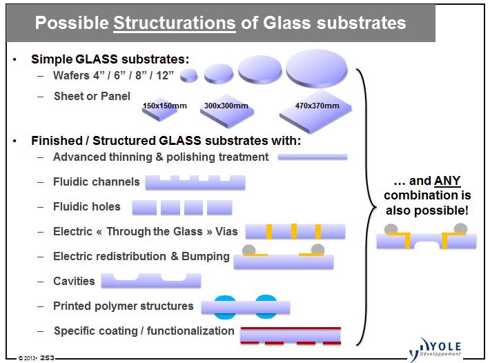
6 Glass Substrate Value Chain Structuration of GLASS Substrates: Simple GLASS: Wafer 4 / 6 / 8 / 12 Sheet or Panel Finished / Structured Wafers with: Advanced thinning & polishing treatment Cavities Fluidic channel Fluidic hole Electric «Through the Glass» Vias Electric redistribution & Bumping Printed polymer structures Specific coating / functionalization Functionnality of GLASS Substrates: Wafer Level Packaging technologies using GLASS: Support substrate WLC WLO 3D TGV/3D glass capping interposers Glass carriers Microstructuring technologies using GLASS: µstructures End Applications for GLASS Substrates: MEMS & Sensors CMOS image sensors LED Modules Memories Logic ICs Analog & RF ICs Microfluidic / Microreaction Micro-batteries / Fuel-cells Power components Concentrated - Solar PV Example of glass value chain in a camera module
7 Functionnalities of Glass substrate wafer versus End applications MEMS CIS LED memory Logic ICs RF/Analog ICs µfluidic Opto comp. Fuel-cells/ µbatteries Power Support Substrate WLC X X X X X X X WLO 3D TGV/ interposer Carriers X X X X X X X X Micro structures X

8 Glass substrate market: 2012 shipments per Application MEMS CIS LED memory Logic ICs RF/Analog ICs µfluidic Opto comp. Fuel-cells/ µbatteries Power Support Substrate 111Kwpy 58Kwpy 2,5Kwpy 0Kwpy WLC 493Kwpy 4,5Kwpy 2,9Mwpy WLO 191Kwpy 3D TGV/ interposer 25Kwpy 0Kwpy 0Kwpy 63Kwpy Carriers 22Kwpy 15Kwpy 53Kwpy Micro structures 210Kwpy
9 Shipments ( in 8 inch eq wspy) Glass substrate overall market size in wspy Breakdown per Functionnalities Glass substrate overall market size (in 8 inch Million wspy) Breakdown per End Application 16 Yole Developpement April Opto components µfluidic RF devices Logic Memory Power LED CIS MEMS
10 2012 Overall market share for glass substrate Glass substrate production for WLP 2012 Market Share Breakdown by glass supplier (in M$) Others HOYA Schott AG AGC Corning $158M Yole Developpement April 2013 PlanOptik Tecnisco Bullen Total market related to the Glass market is assessed at $158M in Schott (G), Tecnisco (JP), PlanOptik (G), Bullen (US) and Corning (US) will share almost 70% of the $158M glass substrate market this year, driven mainly by demand for WLCapping


11 More slides extracts
12 Who should be interested in this report? Equipment & Material suppliers Identify new business opportunities and prospects Understand the differentiated value of your products and technologies in this market Identify technology trends, challenges and precise requirements related to glass substrate Glass substrate manufacturers Evaluate market potential of your technologies and products Position your company in the value chain and market Monitor and benchmark your competitors R&D organizations & Investors Monitor the global activity and consolidation currently happing in the semiconductor equipment & material business in order to identify new partners, targets and take the right decision before committing to one particular supplier IDMs, CMOS foundries & OSAT players Understand technology trends related to glass substrate used in the Wafer-Level-Packaging and Micro structuring technologies

13 About the Authors of this report Amandine Pizzagalli Amandine recently joined Yole Development Advanced Packaging and MEMS manufacturing teams after graduating as an engineer in Electronics, with a specialization in Semiconductors and Nano Electronics Technologies. She worked in the past for Air Liquide with an emphasis on CVD and ALD processes for semiconductor applications Contact: pizzagalli@yole.fr

14 Companies Cited in this Report AGC, Amkor, Anteryon, ASE, Audi, Berliner Glass, Bosch, Bullen, Colorship, Corning, Dolomite, Heptagon, Hoya, Hoya, Honeywell, Hynix, Qualcomm, Ibiden, IMT AG, IPDiA, Infineon, Lemoptix, Microfluidic ChipShop, Micronit, Micron, MikroGlass, Murata, Nemotek, Omnivision, Osram, OptoPac, PlanOptik, Saint-Gobain,Sensonor/Infineon, Samsung, SK Hynix,Statchippac, STMicro, Schott, Sony, SPIL,Tecnisco, Texas Instruments, Toshiba, TSMC, Ulcoat, VisEra, and more


15 Yole activities MEDIA News feed / Magazines / Webcasts REPORTS Market & technology Patent Analysis Reverse costing report CONSULTING Market research Technology & Strategy Patent Analysis YOLE FINANCE M&A / Due Diligence / Fundraising services


16 2010 Copyrights Yole Développement SA. All rights reserved. Our latest market reports Flip-chip 2013 Report 3D Glass & Silicon interposers Report MEMS Packaging Market & Technology Trends N o k i a 6 & 6 mm mm ~25 sq mm ~125 sq mm MEMS Front End Manufacturing Deep RIE Thin Wafer Handling Ferro-Electric Thin Films Flexible & Printed Electronics
17 For More Information Take a look at our websites Yole Développement corporate website News Portal - online free registration to our publications Sister company expert in teardown & reverse costing analysis Separate business unit of Yole dedicated to financial services
Status of Panel Level Packaging & Manufacturing
 From Technologies to Market SAMPLE Status of Panel Level Packaging & Manufacturing Authors: S. Kumar, A. Pizzagalli Source: Fraunhofer IZM Sample 2015 2015 ABOUT THE AUTHORS Biography & contact Santosh
Yole Developpement. Developpement-v2585/ Publisher Sample
 Yole Developpement http://www.marketresearch.com/yole- Developpement-v2585/ Publisher Sample Phone: 800.298.5699 (US) or +1.240.747.3093 or +1.240.747.3093 (Int'l) Hours: Monday - Thursday: 5:30am - 6:30pm
Photonique sur silicium: Tendances et perspectives de marché
 From Technologies to Market Photonique sur silicium: Tendances et perspectives de marché Eric MOUNIER, YOLE DEVELOPPEMENT 2017 FIELDS OF EXPERTISE Yole Développement s 30 analysts operate in the following
The Development of the Semiconductor CVD and ALD Requirement
 The Development of the Semiconductor CVD and ALD Requirement 1 Linx Consulting 1. We create knowledge and develop unique insights at the intersection of electronic thin film processes and the chemicals
Fan-Out Wafer Level Packaging Patent Landscape Analysis
 Fan-Out Wafer Level Packaging Patent Landscape Analysis Source: Infineon Source: TSMC Source: ASE November 2016 Source: Deca Technologies Source: STATS ChipPAC Source: Nepes KnowMade Patent & Technology
The Future of Packaging ~ Advanced System Integration
 The Future of Packaging ~ Advanced System Integration Enabling a Microelectronic World R. Huemoeller SVP, Adv. Product / Platform Develop June 2013 Product Segments End Market % Share Summary 2 New Product
FOR IMMEDIATE RELEASE. Yole s analysts believe in a wide adoption of gas sensors in consumer products
 FOR IMMEDIATE RELEASE Yole s analysts believe in a wide adoption of gas sensors in consumer products Gas Sensor Technology & Market report, February 2016 LYON, France February 11, 2016: The latest analysis
IMPACT OF 450MM ON CMP
 IMPACT OF 450MM ON CMP MICHAEL CORBETT MANAGING PARTNER LINX CONSULTING, LLC MCORBETT@LINX-CONSULTING.COM PREPARED FOR CMPUG JULY 2011 LINX CONSULTING Outline 1. Overview of Linx Consulting 2. CMP Outlook/Drivers
9 rue Alfred Kastler - BP Nantes Cedex 3 - France Phone : +33 (0) website :
 website :") 9 rue Alfred Kastler - BP 10748-44307 Nantes Cedex 3 - France Phone : +33 (0) 240 180 916 - email : info@systemplus.fr - website : www.systemplus.fr April 2012 - Version 1 Written by: Romain FRAUX DISCLAIMER
9 rue Alfred Kastler - BP 10748-44307 Nantes Cedex 3 - France Phone : +33 (0) 240 180 916 - email : info@systemplus.fr - website : www.systemplus.fr April 2012 - Version 1 Written by: Romain FRAUX DISCLAIMER
MICRONEWS MEDIA
 www.i-micronews.com MICRONEWS MEDIA 2013 MediA Kit www.i-micronews.com "Yole Développement has a deep understanding of various technologies, and accounts for all economic parameters in its studies. Our
Plan Optik AG. Plan Optik AG PRODUCT CATALOGUE
 Plan Optik AG Plan Optik AG PRODUCT CATALOGUE 2 In order to service the high demand of wafers more quickly, Plan Optik provides off the shelf products in sizes from 2 up to 300mm diameter. Therefore Plan
MEMS Sensors: From Automotive. CE Applications. MicroNanoTec Forum Innovations for Industry April 19 th Hannover, Germany
 MEMS Sensors: From Automotive to CE Applications MicroNanoTec Forum Innovations for Industry 2010 April 19 th Hannover, Germany Oliver Schatz, CTO 1 Engineering April 2010 GmbH 2009. All rights reserved,
GLOBAL MARKETS, TECHNOLOGIES AND MATERIALS FOR THIN AND ULTRATHIN FILMS
 GLOBAL MARKETS, TECHNOLOGIES AND MATERIALS FOR THIN AND ULTRATHIN FILMS SMC057C August Margareth Gagliardi Project Analyst ISBN: 1-62296-338-5 BCC Research 49 Walnut Park, Building 2 Wellesley, MA 02481
TechSearch International, Inc. Corporate Overview E. Jan Vardaman, President
 TechSearch International, Inc. Corporate Overview E. Jan Vardaman, President Corporate Background Founded in 1987 and headquartered in Austin, Texas Recognized around the world as a leading consulting
SUSS MICROTEC INVESTOR PRESENTATION. February 2014
 SUSS MICROTEC INVESTOR PRESENTATION February 2014 DISCLAIMER This presentation contains forward-looking statements relating to the business, financial performance and earnings of SUSS MicroTec AG and its
The Collaboration Engine: Enabling Innovation in Microelectronics
 The Collaboration Engine: Enabling Innovation in Microelectronics Karen Savala President, SEMI Americas Outline About SEMI Semiconductors: A History of Collaboration Collaboration in other Microelectronics
Update: SOI Wafer Market Continues Its Growth
 Gartner Dataquest Alert Update: SOI Wafer Market Continues Its Growth The results of Gartner Dataquest's latest survey of the silicon on insulator (SOI) wafer market indicate demand grew 16 percent in
Semiconductor and LED Markets. Jon Sabol Vice President and General Manager Semiconductor and LED Division
 Semiconductor and LED Markets Jon Sabol Vice President and General Manager Semiconductor and LED Division Semiconductor & LED Investing in Semiconductor and LED $ Millions 300 200 27% CAGR 100 0 * FY06
ACTIVE IMPLANTS. Glass Encapsulation
 ACTIVE IMPLANTS Glass Encapsulation OUTLINE Smart Implants Overview Cylindrical Glass Encapsulation CGE Planar Glass Encapsulation PGE Platform for Innovative Implantable Devices 5/7/2013 Glass Encapsulation
Lithography in our Connected World
 Lithography in our Connected World SEMI Austin Spring Forum TOP PAN P R INTING CO., LTD MATER IAL SOLUTIONS DIVISION Toppan Printing Co., LTD A Broad-Based Global Printing Company Foundation: January 17,
GaN Power Epitaxy, Devices, Applications and Technology Trends
 From Technologies to Market GaN Power Epitaxy, Devices, Applications and Technology Trends Sample October 2017 Biographies & contacts Dr. Ana Villamor Dr Ana Villamor serves as a Technology & Market Analyst
Photolithography for Advanced Packaging, MEMS & LEDs
 From Technologies to Market Photolithography for Advanced Packaging, MEMS & LEDs Report June 2015 ABOUT THE AUTHORS Biography & contact Amandine PIZZAGALLI, Market & Technology Analyst, Equipment and Materials
Packaging Roadmap: The impact of miniaturization. Bob Pfahl, inemi Celestica-iNEMI Technology Forum May 15, 2007
 Packaging Roadmap: The impact of miniaturization Bob Pfahl, inemi Celestica-iNEMI Technology Forum May 15, 2007 The Challenges for the Next Decade Addressing the consumer experience using the converged
Recent Developments in Multifunctional Integration. Stephan Guttowski, Head of Technology Park»Heterointegration«, Fraunhofer FMD
 Recent Developments in Multifunctional Integration Stephan Guttowski, Head of Technology Park»Heterointegration«, Fraunhofer FMD Founding Participants 2 One-Stop-Shop for developments from wafer technologies
Enabling concepts: Packaging Technologies
 Enabling concepts: Packaging Technologies Ana Collado / Liam Murphy ESA / TEC-EDC 01/10/2018 ESA UNCLASSIFIED - For Official Use Enabling concepts: Packaging Technologies Drivers for the future: Higher
From Technologies to Market. Advanced RF SiP for Cell Phones
 From Technologies to Market Advanced RF SiP for Cell Phones 2017 2017 REPORT METHODOLOGY Market forecast methodology Market segmentation methodology 2017 www.yole.fr Advanced RF SiP for Cell Phones 2017
New Wave SiP solution for Power
 New Wave SiP solution for Power Vincent Lin Corporate R&D ASE Group APEC March 7 th, 2018 in San Antonio, Texas. 0 Outline Challenges Facing Human Society Energy, Environment and Traffic Autonomous Driving
Unit 2 Semiconductor Devices. Lecture_2.5 Opto-Electronic Devices
 Unit 2 Semiconductor Devices Lecture_2.5 Opto-Electronic Devices Opto-electronics Opto-electronics is the study and application of electronic devices that interact with light. Electronics (electrons) Optics
3D ICs: Recent Advances in the Industry
 3D ICs: Recent Advances in the Industry Suresh Ramalingam Senior Director, Advanced Packaging Outline 3D IC Background 3D IC Technology Development Summary Acknowledgements Stacked Silicon Interconnect
Fan-Out Wafer Level Packaging Patent Landscape Analysis
 Fan-Out Wafer Level Packaging Patent Landscape Analysis Source: Infineon Source: TSMC Source: ASE November 2016 Source: Deca Technologies Source: STATS ChipPAC Source: Nepes KnowMade Patent & Technology
The SEMATECH Model: Potential Applications to PV
 Continually cited as the model for a successful industry/government consortium Accelerating the next technology revolution The SEMATECH Model: Potential Applications to PV Dr. Michael R. Polcari President
Electronic Costing & Technology Experts
 Electronic Costing & Technology Experts 21 rue la Nouë Bras de Fer 44200 Nantes France Phone : +33 (0) 240 180 916 email : info@systemplus.fr www.systemplus.fr October 2016 Preliminary Version Written
From Technologies to Market. Laser Technologies for. Semiconductor. Manufacturing. Sample. October 2017
 From Technologies to Market Laser Technologies for Semiconductor Manufacturing Sample October 2017 REPORT OBJECTIVES This report is the first research performed on the laser technologies in the field of
Consumer Physics SCiO Molecular Sensor
 Consumer Physics SCiO Molecular Sensor Pocket handheld spectrometer MEMS/Imaging report by Stéphane ELISABETH February 2017 21 rue la Noue Bras de Fer 44200 NANTES - FRANCE +33 2 40 18 09 16 info@systemplus.fr
Hermetic Packaging Solutions using Borosilicate Glass Thin Films. Lithoglas Hermetic Packaging Solutions using Borosilicate Glass Thin Films
 Hermetic Packaging Solutions using Borosilicate Glass Thin Films 1 Company Profile Company founded in 2006 ISO 9001:2008 qualified since 2011 Headquarters and Production in Dresden, Germany Production
POSSUM TM Die Design as a Low Cost 3D Packaging Alternative
 POSSUM TM Die Design as a Low Cost 3D Packaging Alternative The trend toward 3D system integration in a small form factor has accelerated even more with the introduction of smartphones and tablets. Integration
Noel Technologies. Provider of Advanced Lithography and Semiconductor Thin Film Services
 Noel Technologies Provider of Advanced Lithography and Semiconductor Thin Film Services Noel Technologies Keith Best Biography Over the last 27 years, Keith Best has held a variety of semiconductor processing
Fabricating 2.5D, 3D, 5.5D Devices
 Fabricating 2.5D, 3D, 5.5D Devices Bob Patti, CTO rpatti@tezzaron.com Tezzar on Semiconduct or 04/15/2013 1 Gen4 Dis-Integrated 3D Memory DRAM layers 42nm node 2 million vertical connections per lay per
First Demonstration of Panel Glass Fan-out (GFO) Packages for High I/O Density and High Frequency Multi-Chip Integration
 Packages for High I/O Density and High Frequency Multi-Chip Integration") First Demonstration of Panel Glass Fan-out (GFO) Packages for High I/O Density and High Frequency Multi-Chip Integration Tailong Shi, Chintan Buch,Vanessa Smet, Yoichiro Sato, Lutz Parthier, Frank Wei
First Demonstration of Panel Glass Fan-out (GFO) Packages for High I/O Density and High Frequency Multi-Chip Integration Tailong Shi, Chintan Buch,Vanessa Smet, Yoichiro Sato, Lutz Parthier, Frank Wei
Accelerating Scale Up of Large Area Electronics
 Accelerating Scale Up of Large Area Electronics Duncan Lindsay Business Development Director, CPI 2015 Centre for Process Innovation Limited. All Rights Reserved. Who are CPI? CPI is a UK technology innovation
SiP packaging technology of intelligent sensor module. Tony li
 SiP packaging technology of intelligent sensor module Tony li 2016.9 Contents What we can do with sensors Sensor market trend Challenges of sensor packaging SiP technology to overcome challenges Overview
LED Cost and Technology Trends: How to enable massive adoption in general lighting
 LED Cost and Technology Trends: How to enable massive adoption in general lighting SEMICON West 2011 Moscone Center, San Francisco June 13 th 2011 Lumileds Lumileds OSRAM Aixtron CREE OSRAM OKI OSRAM 45
Electronic Costing & Technology Experts
 Electronic Costing & Technology Experts 21 rue la Nouë Bras de Fer 44200 Nantes France Phone : +33 (0) 240 180 916 email : info@systemplus.fr www.systemplus.fr September 2016 Version 1 Written by Stéphane
STMicroelectronics ToF Proximity Sensor & Flood Illuminator in the Apple iphone X
 STMicroelectronics ToF Proximity Sensor & Flood Illuminator in the Apple iphone X Patent-to-Product Mapping August 2018 KnowMade Patent & Technology Intelligence 2018 www.knowmade.com TABLE OF CONTENTS
David B. Miller Vice President & General Manager September 28, 2005
 Electronic Technologies Business Overview David B. Miller Vice President & General Manager September 28, 2005 Forward Looking Statement During the course of this meeting we may make forward-looking statements.
Flexible Hybrid Electronics Fabricated with High-Performance COTS ICs using RTI CircuitFilm TM Technology
 Flexible Hybrid Electronics Fabricated with High-Performance COTS ICs using RTI CircuitFilm TM Technology Scott Goodwin 1, Erik Vick 2 and Dorota Temple 2 1 Micross Advanced Interconnect Technology Micross
Proceedings. BiTS Shanghai October 21, Archive - Session BiTS Workshop Image: Zhu Difeng/Dollar Photo Club
 Proceedings Archive - Session 1 2015 BiTS Workshop Image: Zhu Difeng/Dollar Photo Club Proceedings With Thanks to Our Sponsors! Premier Honored Distinguished Publication Sponsor 2 Proceedings Presentation
Disruptive Developments for Advanced Die Attach to Tackle the Challenges of Heterogeneous Integration
 Disruptive Developments for Advanced Die Attach to Tackle the Challenges of Heterogeneous Integration Hugo Pristauz & Andreas Mayr, Besi Austria presented by: Stefan Behler, Besi Switzerland ECTC 2018
Technology & Manufacturing
 Technology & Manufacturing Jean-Marc Chery Chief Operating Officer Front-End Manufacturing Unique capability 2 Technology portfolio aligned with application focus areas Flexible IDM model with foundry
Specialization in Microelectronics. Wang Qijie Nanyang Assistant Professor in EEE March 8, 2013
 Specialization in Microelectronics Wang Qijie Nanyang Assistant Professor in EEE qjwang@ntu.edu.sg March 8, 2013 Electronic Engineering Option Microelectronics What is it about? Study of semiconductor
All-Glass Gray Scale PhotoMasks Enable New Technologies. Che-Kuang (Chuck) Wu Canyon Materials, Inc.
 Wu Canyon Materials, Inc.") All-Glass Gray Scale PhotoMasks Enable New Technologies Che-Kuang (Chuck) Wu Canyon Materials, Inc. 1 Overview All-Glass Gray Scale Photomask technologies include: HEBS-glasses and LDW-glasses HEBS-glass
All-Glass Gray Scale PhotoMasks Enable New Technologies Che-Kuang (Chuck) Wu Canyon Materials, Inc. 1 Overview All-Glass Gray Scale Photomask technologies include: HEBS-glasses and LDW-glasses HEBS-glass
MEMS in ECE at CMU. Gary K. Fedder
 MEMS in ECE at CMU Gary K. Fedder Department of Electrical and Computer Engineering and The Robotics Institute Carnegie Mellon University Pittsburgh, PA 15213-3890 fedder@ece.cmu.edu http://www.ece.cmu.edu/~mems
RF GaN Market. Applications, players, devices, and technologies
 RF GaN Market Applications, players, devices, and technologies 2018 2023 RF GaN Market Sample www.yole.fr 2018 REPORT OBJECTIVES Provide an overview of the RF GaN market. Analyze different players in different
A Low-cost Through Via Interconnection for ISM WLP
 A Low-cost Through Via Interconnection for ISM WLP Jingli Yuan, Won-Kyu Jeung, Chang-Hyun Lim, Seung-Wook Park, Young-Do Kweon, Sung Yi To cite this version: Jingli Yuan, Won-Kyu Jeung, Chang-Hyun Lim,
Uncooled Infrared Imagers Technology & Market Trends 2017
 From Technologies to Market Uncooled Infrared Imagers Technology & Market Trends 2017 Sample August 2017 TABLE OF CONTENTS Glossary, definitions, scope & report objectives 4 Executive summary 9 Introduction
9 rue Alfred Kastler - BP Nantes Cedex 3 - France Phone : +33 (0) website :
 website :") 9 rue Alfred Kastler - BP 10748-44307 Nantes Cedex 3 - France Phone : +33 (0) 240 180 916 - email : info@systemplus.fr - website : www.systemplus.fr May 2012 - Version 1 Written by: Sylvain HALLEREAU DISCLAIMER
9 rue Alfred Kastler - BP 10748-44307 Nantes Cedex 3 - France Phone : +33 (0) 240 180 916 - email : info@systemplus.fr - website : www.systemplus.fr May 2012 - Version 1 Written by: Sylvain HALLEREAU DISCLAIMER
Electronic Costing & Technology Experts
 Electronic Costing & Technology Experts 21 rue la Nouë Bras de Fer 44200 Nantes France Phone : +33 (0) 240 180 916 email : info@systemplus.fr www.systemplus.fr April 2016 - Version 1 written by Stéphane
Apple iphone X IR Dot Projector
 Apple iphone X IR Dot Projector Dot Projector bundle including Heptagon Imaging report by Sylvain HALLEREAU December 2017 21 rue la Noue Bras de Fer 44200 NANTES - FRANCE +33 2 40 18 09 16 info@systemplus.fr
ASML Market dynamics. Dave Chavoustie EVP Sales Analyst Day, September 30, 2004
 ASML Market dynamics Dave Chavoustie EVP Sales Analyst Day, September 30, 2004 Agenda! Market Overview! Growth Opportunities! 300mm Market! Asia Overview / Slide 2 ASML Unit Market Share Trend 60% 12 &
RF MEMS To Enhance Telecommunications 1/23
 RF MEMS To Enhance Telecommunications 1/23 11 Rue destrategy l Harmonie - 59650 d Ascq - France Officer. - T: (+33) 320 050Founder 545 - F: (+33) 320 050 704 - www.delfmems.comapril, 2013 - Olivier Millet,
Inertial MEMS Manufacturing Trends 2014 report Volumes 1 & 2 From Yole Développement
 For immediate release: 6 and 9-axis DOF sensors are creating a new paradigm in the combos business Inertial MEMS Manufacturing Trends 2014 report Volumes 1 & 2 From Yole Développement Lyon, France - March
9 rue Alfred Kastler - BP Nantes Cedex 3 - France Phone : +33 (0) website :
 website :") 9 rue Alfred Kastler - BP 10748-44307 Nantes Cedex 3 - France Phone : +33 (0) 240 180 916 - email : info@systemplus.fr - website : www.systemplus.fr December 2010 - Version 1 Written by: Romain FRAUX DISCLAIMER
9 rue Alfred Kastler - BP 10748-44307 Nantes Cedex 3 - France Phone : +33 (0) 240 180 916 - email : info@systemplus.fr - website : www.systemplus.fr December 2010 - Version 1 Written by: Romain FRAUX DISCLAIMER
Triple i - The key to your success
 Triple i - The key to your success The needs and challenges of today s world are becoming ever more demanding. Standards are constantly rising. Creativity, reliability and high performance are basic prerequisites
Apple iphone 6s Plus Teardown & Physical Analyses of Key Components
 Apple iphone 6s Plus Teardown & Physical Analyses of Key Components Discover and understand Apple s technical choices and main suppliers The Apple iphone 6s Plus holds many IC components which are listed
Growing the Semiconductor Industry in New York: Challenges and Opportunities
 Accelerating the next technology revolution The SEMATECH New York Experience Growing the Semiconductor Industry in New York: Challenges and Opportunities Dan Armbrust President and CEO, SEMATECH April
Industrialization of Micro-Electro-Mechanical Systems. Werner Weber Infineon Technologies
 Industrialization of Micro-Electro-Mechanical Systems Werner Weber Infineon Technologies Semiconductor-based MEMS market MEMS Market 2004 (total 22.7 BUS$) Others mostly Digital Light Projection IR Sensors
4G HIGH PERFORMANCE WITH A SMALL CHIP ANTENNA?
 4G HIGH PERFORMANCE WITH A SMALL CHIP ANTENNA? RUN mxtend TM & SmarTune TM - Antenna Component: RUN mxtend TM FR01-S4-244 - Dimensions: 12.0 mm x 3.0 mm x 2.4 mm - Frequency regions: 698-960 MHz & 1710-2690
SEMI Connects: An Overview of SEMI Worldwide. Theresia Fasinski - Manager Membership Relations, SEMI Europe
 SEMI Connects: An Overview of SEMI Worldwide Theresia Fasinski - Manager Membership Relations, SEMI Europe SEMI Connects to Advance a Global Industry Mission SEMI provides industry stewardship and engages
WLP Probing Technology Opportunity and Challenge. Clark Liu
 WLP Probing Technology Opportunity and Challenge Founded Capital PTI Group Overview : May/15/97 : USD 246 Millions PTI HQ Total Assets : USD 2.2B Employees Major Services : 11,100 (Greatek included) :
Fraunhofer IZM - ASSID
 FRAUNHOFER-INSTITUT FÜR Zuverlässigkeit und Mikrointegration IZM Fraunhofer IZM - ASSID All Silicon System Integration Dresden Heterogeneous 3D Wafer Level System Integration 3D system integration is one
Through Glass Via (TGV) Technology for RF Applications
 Technology for RF Applications") Through Glass Via (TGV) Technology for RF Applications C. H. Yun 1, S. Kuramochi 2, and A. B. Shorey 3 1 Qualcomm Technologies, Inc. 5775 Morehouse Dr., San Diego, California 92121, USA Ph: +1-858-651-5449,
Through Glass Via (TGV) Technology for RF Applications C. H. Yun 1, S. Kuramochi 2, and A. B. Shorey 3 1 Qualcomm Technologies, Inc. 5775 Morehouse Dr., San Diego, California 92121, USA Ph: +1-858-651-5449,
Property right statement: Copyright of charts, tables and sentences in this report belongs to
 The Vertical Portal for China Business Intelligence. Semiconductor Equipment Industry Report, 2009 Nov/2009 Property right statement: Copyright of charts, tables and sentences in this report belongs to
Processes for Flexible Electronic Systems
 Processes for Flexible Electronic Systems Michael Feil Fraunhofer Institut feil@izm-m.fraunhofer.de Outline Introduction Single sheet versus reel-to-reel (R2R) Substrate materials R2R printing processes
Electronic Components (Elements)
") Lecture_3 Electronic Components (Elements) Instructor: IBRAHIM ABU-ISBEIH 25 July 2011 Reverse Engineering 1 Objectives: After completing this class, you will be able to identify the most commonly used
Lecture_3 Electronic Components (Elements) Instructor: IBRAHIM ABU-ISBEIH 25 July 2011 Reverse Engineering 1 Objectives: After completing this class, you will be able to identify the most commonly used
Reducing MEMS product development and commercialization time
 Reducing MEMS product development and commercialization time Introduction Fariborz Maseeh, Andrew Swiecki, Nora Finch IntelliSense Corporation 36 Jonspin Road, Wilmington MA 01887 www.intellisense.com
Emerging Non-Volatile Memories Patent Landscape February 2014
 Emerging Non-Volatile Memories Patent Landscape February 2014 IBM University of Houston IBM Integrated Magneto Electronics Macronix IBM SanDisk 2405 route des Dolines 06902 Sophia Antipolis, France www.knowmade.com
Wah Lee Industrial Corp. was founded in In order to integrate the industry development of Taiwan with the overall operation requirement of Wah
 2010 10 Wah Lee Industrial Corp. was founded in 1968. In order to integrate the industry development of Taiwan with the overall operation requirement of Wah Lee, we defined our mission as "Introduce and
Image Sensor Advanced Package Solution. Prepared by : JL Huang & KingPak RD division
 Image Sensor Advanced Package Solution Prepared by : JL Huang & KingPak RD division Contents CMOS image sensor marketing overview Comparison between different type of CMOS image sensor package Overview
Image sensor combining the best of different worlds
 Image sensors and vision systems Image sensor combining the best of different worlds First multispectral time-delay-and-integration (TDI) image sensor based on CCD-in-CMOS technology. Introduction Jonathan
ams Multi-Spectral Sensor True Color ambient light sensor from Apple iphone X
 ams Multi-Spectral Sensor True Color ambient light sensor from Apple iphone X IMAGING report by Stéphane ELISABETH December 2017 version 1 21 rue la Noue Bras de Fer 44200 NANTES - FRANCE +33 2 40 18 09
450mm and Moore s Law Advanced Packaging Challenges and the Impact of 3D
 450mm and Moore s Law Advanced Packaging Challenges and the Impact of 3D Doug Anberg VP, Technical Marketing Ultratech SOKUDO Lithography Breakfast Forum July 10, 2013 Agenda Next Generation Technology
Application-Based Opportunities for Reused Fab Lines
 Application-Based Opportunities for Reused Fab Lines Semicon China, March 17 th 2010 Keith Best Simax Lithography S I M A X A L L I A N C E P A R T N E R S Outline Market: Exciting More than Moore applications
J.S. Whang Executive Chairman. Fokko Pentinga President & CEO. Solar Semiconductor LED
 J.S. Whang Executive Chairman Fokko Pentinga President & CEO Solar Semiconductor LED 1 Safe Harbor Statement This Presentation may contain certain statements or information that constitute forward-looking
Advances in CO 2 -Laser Drilling of Glass Substrates
 Available online at www.sciencedirect.com Physics Procedia 39 (2012 ) 548 555 LANE 2012 Advances in CO 2 -Laser Drilling of Glass Substrates Lars Brusberg,a, Marco Queisser b, Clemens Gentsch b, Henning
SEMI and Yole Développement Present: Smart Automotive Latest Trends in LiDAR and Sensors
 SEMI and Yole Développement Present: Smart Automotive Latest Trends in LiDAR and Sensors Bettina Weiss Vice President, Business Development SEMI Global Headquarters SEMI Connects to Advance the Global
Accelerating Growth and Cost Reduction in the PV Industry
 Accelerating Growth and Cost Reduction in the PV Industry PV Technology Roadmaps and Industry Standards An Association s Approach Bettina Weiss / SEMI PV Group July 29, 2009 SEMI : The Global Association
Semiconductor Process Diagnosis and Prognosis for DSfM
 Semiconductor Process Diagnosis and Prognosis for DSfM Department of Electronic Engineering Prof. Sang Jeen Hong Nov. 19, 2014 1/2 Agenda 1. Semiconductor Manufacturing Industry 2. Roles of Semiconductor
Used Semiconductor Manufacturing Equipment: Looking for Sales in All the Right Places. Study Number MA108-09
 Study Number MA108-09 August 2009 Copyright Semico Research, 2009. All rights reserved. Reproduction in whole or part is prohibited without permission of Semico. The contents of this report represent
Sony IMX145 8 Mp, 1.4 µm Pixel Pitch Back Illuminated (BSI) CMOS Image Sensor from the Apple iphone 4S Smartphone
 CMOS Image Sensor from the Apple iphone 4S Smartphone") Sony IMX145 8 Mp, 1.4 µm Pixel Pitch Back Illuminated (BSI) CMOS Image Sensor from the Apple iphone 4S Smartphone Imager Process Review 3685 Richmond Road, Suite 500, Ottawa, ON K2H 5B7 Canada Tel: 613-829-0414
Sony IMX145 8 Mp, 1.4 µm Pixel Pitch Back Illuminated (BSI) CMOS Image Sensor from the Apple iphone 4S Smartphone Imager Process Review 3685 Richmond Road, Suite 500, Ottawa, ON K2H 5B7 Canada Tel: 613-829-0414
Autoliv Night Vision System Safety Application Automotive IR Camera
 Autoliv Night Vision System Safety Application Automotive IR Camera Report by Farid HAMRANI & Sylvain HALLEREAU June 2017 21 rue la Noue Bras de Fer 44200 NANTES - FRANCE +33 2 40 18 09 16 info@systemplus.fr
3D SOI elements for System-on-Chip applications
 Advanced Materials Research Online: 2011-07-04 ISSN: 1662-8985, Vol. 276, pp 137-144 doi:10.4028/www.scientific.net/amr.276.137 2011 Trans Tech Publications, Switzerland 3D SOI elements for System-on-Chip
TSI, or through-silicon insulation, is the
 Vertical through-wafer insulation: Enabling integration and innovation PETER HIMES, Silex Microsystems AB, Järfälla SWEDEN Through-wafer insulation has been used to develop technologies such as Sil-Via
Glass: Enabling Next-Generation, Higher Performance Solutions. Peter L. Bocko, Ph.D CTO Glass Technologies 5 September 2012
 Glass: Enabling Next-Generation, Higher Performance Solutions Peter L. Bocko, Ph.D CTO Glass Technologies 5 September 2012 Forward Looking And Cautionary Statements Certain statements in this presentation
Developing Smart Miniaturized Solutions for Industry
 Developing Smart Miniaturized Solutions for Industry Micro nanotechnologies & Embedded Software Competitive Cluster - Grenoble / France www.minalogic.com Born in Grenoble 1 st french scanner (1972) Airbag
Camera Module Industry 2017
 From Technologies to Market Camera Module Industry 2017 Sample November 2017 ABOUT THE AUTHORS OF THIS REPORT Biography & contact Pierre Cambou Pierre Cambou joined the imaging industry in 1999. Following
Chapter 7 Introduction to 3D Integration Technology using TSV
 Chapter 7 Introduction to 3D Integration Technology using TSV Jin-Fu Li Department of Electrical Engineering National Central University Jungli, Taiwan Outline Why 3D Integration An Exemplary TSV Process
MULTIMEDIA TOOL FOR UNDERSTANDING AND EXPLAINING MICROSYSTEMS
 MULTIMEDIA TOOL FOR UNDERSTANDING AND EXPLAINING MICROSYSTEMS PHILIPPE FISCHER and MARCEL ECABERT, FSRM, Neuchâtel, Switzerland MICHEL BERGER, mib génie logiciel, Neuchâtel, Switzerland ERIC MOUNIER, YOLE
Let me also remind you the two on-going challenges until 30 th June for the ASPICS and for Custom products. Take your chance!
 Dear Partners, The first term of this year has been marked by a sharp intensification in direct communication through worldwide exhibitions. IPDiA products and technologies have been displayed in more
The Future for Printed Electronics
 The Future for Printed Electronics Jon Helliwell National Centre for Printable Electronics 24 October, 2013 Copyright CPI 2013. All rights reserved What is Printed Electronics? Organic and printed electronics
Complementary Organic Semiconductor and Metal Integrated Circuits
 Complementary Organic Semiconductor and Metal Integrated Circuits COSMIC will generate an organic CMOS technology platform from design to manufacturing level. COSMIC will produce highly complex lead applications