Smart Devices of 2025
|
|
|
- Dylan Potter
- 5 years ago
- Views:
Transcription

1 Smart Devices of 2025 Challenges for Packaging of Future Device Technologies Steve Riches/Kevin Cannon Tribus-D Ltd CW Workshop 27 March 2018 E:mail: M:


2 Assembly Technology Development Advanced Electronic Packaging and Interconnect: Distributed (Smart) Systems Miniaturisation Reduced parasitics Elimination of interfaces Flexible hybrid electronics (Si/passive devices) Rapid prototyping Tribus-D Ltd Overview Specialists in Micro-Electronics Assembly Founded January 2016 Assembly Technology Consultancy 3D Interconnects Image: Optomec Packaging and Interconnect: 3D Interconnect Die Attach Sintering Die Thinning Flip Chip Bonding Wire Bonding Adhesives/soldering Over-moulding Thermal Management Underfill Over 60 years combined industrial experience in: Electronic packaging and interconnection Automotive, industrial, aerospace and consumer electronics Si, SiC, GaN semiconductor assembly Optics, Sensors, MEMS, ASICs, Power, Hybrids Displays, LED lighting High temperature electronic packaging Energy harvesting Wireless interconnect Laser processing Project management Proposal generation Kevin Cannon Steve Riches Tribus-D Overview, February 2018


3 Scope of Presentation Advanced Packaging of Electronic Devices More than Moore Technology Trends Commercial Challenges Wide Band-gap Semiconductors Heterogeneous Integration on Foils Fan Out Wafer Level Packaging (FOWLP) 5G/SIP Architectures Additional Challenges of RF/µ-Wave/mm-Wave Packaging for Future Devices Miniaturisation Embedded Packaging Technologies Plastic and Hybrid Electronics Additive Manufacturing/3D Printing Conclusions
4

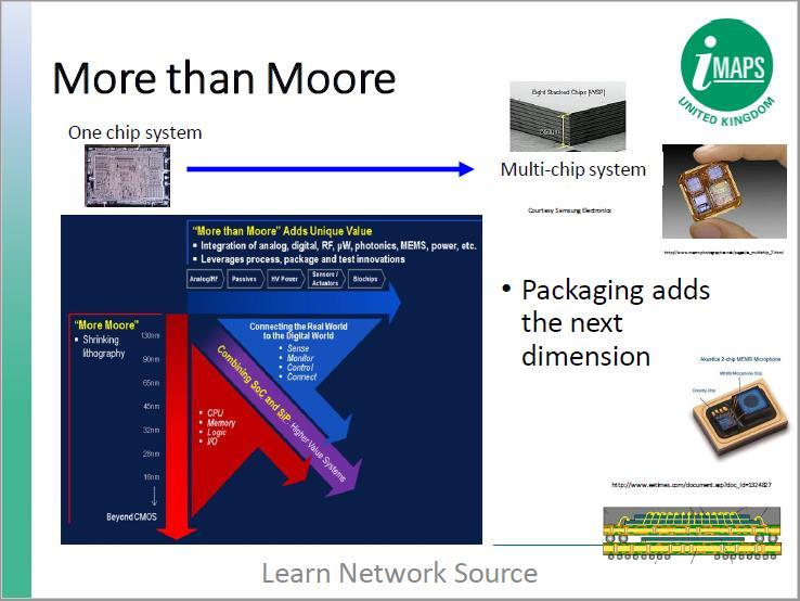
5 Advanced Packaging Assembly Methods Technology Trends Higher power Higher frequencies Thermal management EMI shielding Miniaturisation/form factor More integration/embedding Less bespoke products Higher quantities End of Life/Recycling Material availability Sustainability Flexible/Hybrid electronics Cross-Section of Advanced Packaging Assembly Methods Image: Yole Development

6 Commercial Challenges for Industrialisation Materials and manufacturing costs Economies of scale Low volume vs high volume Established supply chain In-house manufacture vs sub-contract Standard vs customised product Investment required Level of integration Low power vs high power Availability of bare die Minimum order quantities Yield Obsolescence Cost modelling Patent issues System in Package Options Source: O Malley G, i-nemi Packaging Trends and Challenges Microtech 17, IMAPS-UK, March 2017, Rutherford Appleton Laboratories
 and thermal resistance Achieved by shortening connections and removal of")
7 Potential Applications for Wide Band-Gap Semiconductors As power capacity and operating frequencies increase, packaging and interconnection becomes more important in determining performance and efficiency of power modules Need to reduce circuit parasitics (R, C, L) and thermal resistance Achieved by shortening connections and removal of interfaces

8 Smart System Integration on foils

")
")
 Bottom side Thin")
 and Antenna on foil")
9 Multi-foil Hetereogeneous Integration Thin voltage regulator 2xSTLQ50 (STMicroelectronics) Top side flexible PV panel Printed Sensors (FhG EMFT) Wiring layers, Printed via holes, Passives and Assembly (FhG EMFT, Bosch) Thinned STM8L Microcontroller (STMicroelectronics) Bottom side Thin film batteries (CEA Liten) Radio chip (bare die) and Antenna on foil EC-funded FP7 project Interflex ( )
10
11
12

13 Qualcomm VIVE QCA9500 High Density WiGig/WiFi Chipset for 60GHz Band RF IC and Integrated Antennae Up to 4 transceivers controlling up to 32 antennae Antennae embedded within package SiP with double sided moulded configuraton Baseboard processor re-distributed processor signal to pcb with copper pillars inside the moulding Switch Regulator Crystal Memory 60 SMD components

14 Additional Challenges for RF/µ-wave/mm-wave Packaging: Distributed Effects Circuit features/components have dimensions that are appreciable fraction of the wavelength Electrical characteristics change as the frequency increases Small features or discontinuities in signal traces can have a significant effect on circuit performance Ref: Kuang K, Franklin K and Cahill S RF and Microwave Microelectronics Packaging Springer Publishing ISBN

15 Additional Challenges for RF/µ-wave/mm-wave Packaging: Transmission line and interconnection via signal transition effects Coupling and radiation: adjacent metal traces, traces near to ICs, traces between layers Materials selection: line impedance and insertion loss, thickness of dielectric and metal layers Lumped elements: passives need to be integrated or embedded into the packaging to perform at higher frequencies Design of metal pattern and dielectric thickness to maintain required line impedance Short interconnect lengths to minimise reflections Material selection to minimise effects on electromagnetic fields on ICs Coupling between traces and package resonance High power dissipation from active devices Sensitivity of some devices to mechanical damage Microwave Evaluation Board Image: Ref: Kuang K, Franklin K and Cahill S RF and Microwave Microelectronics Packaging Springer Publishing ISBN


16 Packaging Trends - Miniaturisation Thinned die <50µm Die Connections <30µm 2.5D and 3D structures Alignment sub-micron Thermal management Features Handling thinned silicon die Levelling/parallelism Package warpage Alignment tolerances CTE mismatch Barriers Ref: O Malley G, i-nemi Packaging Trends and Challenges Microtech 17, IMAPS-UK, March 2017, Rutherford Appleton Laboratories Ref: Avrillier C, SET Flip-chip bonding : how to meet the high accuracy requirement? Advanced Packaging Workshop, IMAPS-UK, Feb 18

17 Alternative Assembly Methods for Flip Chip
 has higher remelt temperature Advantages Low cost materials compared to Ag or Au High thermal stability Remelt temperatures higher than process temperatures Disadvantages Long processing")
18 Overview of Transient Liquid Phase (TLPS) Cu-Sn Solder Bonding Process Process Description Heating, melting and dissolution/diffusion of low melting point material (e.g. Sn) with Cu Sn can be applied as: Foil Separate particles Sn coated Cu particles Intermetallic joint formed (e.g. Cu 3 Sn) has higher remelt temperature Advantages Low cost materials compared to Ag or Au High thermal stability Remelt temperatures higher than process temperatures Disadvantages Long processing times normally required to achieve Cu-Sn intermetallic joint Intermetallic materials have high rigidity, possibly causing stresses during thermal cycling Complicated processing involving pressure and removal of oxide prior to bonding (e.g. through formic acid) Difficult to achieve void free interfaces Ref: Nishikawa H et al Effect of Iso-Thermal Aging at 250 o C on shear strength of joints using Sn coated Cu Particle Paste for High Temperature Application, HITEN 2017 Conference pp

19 Packaging Trends Embedded Packaging Technologies Features Design flexibility Common building blocks modular electronics Reduced module thickness Improved electrical performance EMI shielding capability Barriers CTE mismatch between Si and substrate Possibility of repair Recyclability/sustainability Thermal management Yields Ref: Ivankovic A et al, Yole Developments Status of advanced substrates 2018 Embedded dies and interconnects, substrates like pcb trends March 2018 Ref: Tremlett P, Micro-semi Why Embedded Die IMAPS-UK/NMI Conference Embedded Die Technology, September 2016


20 Embedded Electronic Packaging Technologies for Compound Semiconductor Power Applications Technology Features Integrated power module Common building block Modular and scalable Thermal management Potential Benefits Miniaturisation Improved electrical efficiency Enhanced heat dissipation and EMI shielding High temperature operation Recyclability and sustainability What s Next Demonstration End-User Feedback Benchmarking Collaboration IP Landscape


21 Packaging Trends Plastic and Hybrid Electronics Wearable healthcare Device Source: medgadget Features Plastic ICs for limited functionality (e.g. RFID) Combination of Si and plastics for higher performance Opportunity for introduction of new materials High volume, low cost applications Silicon on Flex Demonstrator Source: Imperial College Barriers Integration of diverse materials Low overall temperature processing Low temperature excursions Localised heating techniques Reliability/lifetime Ref: Dou G and Holmes A, Imperial College Interconnection Technologies for Integration of Active Devices with Printed Plastic Electronics InnoLAE Conference, Cambridge, January 2018

22 Packaging Trends Additive Manufacturing/3D Printing Features Ref: Berger U Additive Manufacturing to Add Value to Products Produced with Conventional Manufacturing Methods IMAPS-UK Microtech, March 2017
23 Challenges for Packaging of Future Device Technologies - Conclusions Increased power and frequency requirements for future electronic modules will need: Enhanced thermal management Reduced circuit parasitics Improved EMI shielding For companies wishing to exploit devices using advanced packaging technologies, affordable access to state of the art packaging equipment is needed in the following areas: Miniaturisation Embedded Packaging Technologies Plastic and Hybrid Electronics Additive Manufacturing/3D printing Routes to industrialisation need to be defined between: Lower volume, high added value Higher volume, low cost applications Different business models may be required
The Future of Packaging ~ Advanced System Integration
 The Future of Packaging ~ Advanced System Integration Enabling a Microelectronic World R. Huemoeller SVP, Adv. Product / Platform Develop June 2013 Product Segments End Market % Share Summary 2 New Product
Recent Developments in Multifunctional Integration. Stephan Guttowski, Head of Technology Park»Heterointegration«, Fraunhofer FMD
 Recent Developments in Multifunctional Integration Stephan Guttowski, Head of Technology Park»Heterointegration«, Fraunhofer FMD Founding Participants 2 One-Stop-Shop for developments from wafer technologies
Flexible Hybrid Electronics Fabricated with High-Performance COTS ICs using RTI CircuitFilm TM Technology
 Flexible Hybrid Electronics Fabricated with High-Performance COTS ICs using RTI CircuitFilm TM Technology Scott Goodwin 1, Erik Vick 2 and Dorota Temple 2 1 Micross Advanced Interconnect Technology Micross
Laminate Based Fan-Out Embedded Die Technologies: The Other Option
 Laminate Based Fan-Out Embedded Die Technologies: The Other Option Theodore (Ted) G. Tessier, Tanja Karila*, Tuomas Waris*, Mark Dhaenens and David Clark FlipChip International, LLC 3701 E University Drive
Packaging Roadmap: The impact of miniaturization. Bob Pfahl, inemi Celestica-iNEMI Technology Forum May 15, 2007
 Packaging Roadmap: The impact of miniaturization Bob Pfahl, inemi Celestica-iNEMI Technology Forum May 15, 2007 The Challenges for the Next Decade Addressing the consumer experience using the converged
Diverse Lasers Support Key Microelectronic Packaging Tasks
 Diverse Lasers Support Key Microelectronic Packaging Tasks Written by D Muller, R Patzel, G Oulundsen, H Halou, E Rea 23 July 2018 To support more sophisticated and compact tablets, phones, watches and
Fraunhofer IZM - ASSID
 FRAUNHOFER-INSTITUT FÜR Zuverlässigkeit und Mikrointegration IZM Fraunhofer IZM - ASSID All Silicon System Integration Dresden Heterogeneous 3D Wafer Level System Integration 3D system integration is one
Flip-Chip for MM-Wave and Broadband Packaging
 1 Flip-Chip for MM-Wave and Broadband Packaging Wolfgang Heinrich Ferdinand-Braun-Institut für Höchstfrequenztechnik (FBH) Berlin / Germany with contributions by F. J. Schmückle Motivation Growing markets
SESUB - Its Leadership In Embedded Die Packaging Technology
 SESUB - Its Leadership In Embedded Die Packaging Technology Sip Conference China 2018 TDK Corporation ECBC, PAF, SESUB BU Kofu, Japan October 17, 2018 Contents SESUB Introduction SESUB Process SESUB Quality
POSSUM TM Die Design as a Low Cost 3D Packaging Alternative
 POSSUM TM Die Design as a Low Cost 3D Packaging Alternative The trend toward 3D system integration in a small form factor has accelerated even more with the introduction of smartphones and tablets. Integration
Yole Developpement. Developpement-v2585/ Publisher Sample
 Yole Developpement http://www.marketresearch.com/yole- Developpement-v2585/ Publisher Sample Phone: 800.298.5699 (US) or +1.240.747.3093 or +1.240.747.3093 (Int'l) Hours: Monday - Thursday: 5:30am - 6:30pm
High Efficient Heat Dissipation on Printed Circuit Boards. Markus Wille, R&D Manager, Schoeller Electronics Systems GmbH
 High Efficient Heat Dissipation on Printed Circuit Boards Markus Wille, R&D Manager, Schoeller Electronics Systems GmbH m.wille@se-pcb.de Introduction 2 Heat Flux: Q x y Q z The substrate (insulation)
5G Systems and Packaging Opportunities
 5G Systems and Packaging Opportunities Rick Sturdivant, Ph.D. Founder and Chief Technology Officer MPT, Inc. (www.mptcorp.com), ricksturdivant@gmail.com Abstract 5G systems are being developed to meet
Fan-Out Solutions: Today, Tomorrow the Future Ron Huemoeller
 Fan-Out Solutions: Today, Tomorrow the Future Ron Huemoeller Corporate Vice President, WW RnD & Technology Strategy 1 In the Beginning ewlb 2 Fan Out Packaging Emerges Introduction of Fan Out (ewlb) Marketed
SiP packaging technology of intelligent sensor module. Tony li
 SiP packaging technology of intelligent sensor module Tony li 2016.9 Contents What we can do with sensors Sensor market trend Challenges of sensor packaging SiP technology to overcome challenges Overview
3D ICs: Recent Advances in the Industry
 3D ICs: Recent Advances in the Industry Suresh Ramalingam Senior Director, Advanced Packaging Outline 3D IC Background 3D IC Technology Development Summary Acknowledgements Stacked Silicon Interconnect
Processes for Flexible Electronic Systems
 Processes for Flexible Electronic Systems Michael Feil Fraunhofer Institut feil@izm-m.fraunhofer.de Outline Introduction Single sheet versus reel-to-reel (R2R) Substrate materials R2R printing processes
!"#$"%&' ()#*+,-+.&/0(
#*+,-+.&/0(") !"#$"%&' ()#*+,-+.&/0( Multi Chip Modules (MCM) or Multi chip packaging Industry s first MCM from IBM. Generally MCMs are horizontal or two-dimensional modules. Defined as a single unit containing two
!"#$"%&' ()#*+,-+.&/0( Multi Chip Modules (MCM) or Multi chip packaging Industry s first MCM from IBM. Generally MCMs are horizontal or two-dimensional modules. Defined as a single unit containing two
Innovations Push Package-on-Package Into New Markets. Flynn Carson. STATS ChipPAC Inc Kato Rd Fremont, CA 94538
 Innovations Push Package-on-Package Into New Markets by Flynn Carson STATS ChipPAC Inc. 47400 Kato Rd Fremont, CA 94538 Copyright 2010. Reprinted from Semiconductor International, April 2010. By choosing
Plan Optik AG. Plan Optik AG PRODUCT CATALOGUE
 Plan Optik AG Plan Optik AG PRODUCT CATALOGUE 2 In order to service the high demand of wafers more quickly, Plan Optik provides off the shelf products in sizes from 2 up to 300mm diameter. Therefore Plan
A Miniaturized Multi-Channel TR Module Design Based on Silicon Substrate
 Progress In Electromagnetics Research Letters, Vol. 74, 117 123, 2018 A Miniaturized Multi-Channel TR Module Design Based on Silicon Substrate Jun Zhou 1, 2, *, Jiapeng Yang 1, Donglei Zhao 1, and Dongsheng
High Frequency Single & Multi-chip Modules based on LCP Substrates
 High Frequency Single & Multi-chip Modules based on Substrates Overview Labtech Microwave has produced modules for MMIC s (microwave monolithic integrated circuits) based on (liquid crystal polymer) substrates
Organic Packaging Substrate Workshop Overview
 Organic Packaging Substrate Workshop Overview Organized by: International Electronics Manufacturing Initiative (inemi) Mario A. Bolanos November 17-18, 2009 1 Organic Packaging Substrate Workshop Work
First Demonstration of Panel Glass Fan-out (GFO) Packages for High I/O Density and High Frequency Multi-Chip Integration
 Packages for High I/O Density and High Frequency Multi-Chip Integration") First Demonstration of Panel Glass Fan-out (GFO) Packages for High I/O Density and High Frequency Multi-Chip Integration Tailong Shi, Chintan Buch,Vanessa Smet, Yoichiro Sato, Lutz Parthier, Frank Wei
First Demonstration of Panel Glass Fan-out (GFO) Packages for High I/O Density and High Frequency Multi-Chip Integration Tailong Shi, Chintan Buch,Vanessa Smet, Yoichiro Sato, Lutz Parthier, Frank Wei
TechSearch International, Inc. Corporate Overview E. Jan Vardaman, President
 TechSearch International, Inc. Corporate Overview E. Jan Vardaman, President Corporate Background Founded in 1987 and headquartered in Austin, Texas Recognized around the world as a leading consulting
MID Manufacturing Process.
 3D Aerosol Jet Printing An Emerging MID Manufacturing Process. Dr. Martin Hedges Neotech Services MTP, Nuremberg, Germany info@neotechservices.com Aerosol Jet Printing Aerosol Jet Process Overview Current
Semiconductor and LED Markets. Jon Sabol Vice President and General Manager Semiconductor and LED Division
 Semiconductor and LED Markets Jon Sabol Vice President and General Manager Semiconductor and LED Division Semiconductor & LED Investing in Semiconductor and LED $ Millions 300 200 27% CAGR 100 0 * FY06
Market and technology trends in advanced packaging
 Close Market and technology trends in advanced packaging Executive OVERVIEW Recent advances in device miniaturization trends have placed stringent requirements for all aspects of product manufacturing.
3D Integration Using Wafer-Level Packaging
 3D Integration Using Wafer-Level Packaging July 21, 2008 Patty Chang-Chien MMIC Array Receivers & Spectrographs Workshop Pasadena, CA Agenda Wafer-Level Packaging Technology Overview IRAD development on
ICT Micro- and nanoelectronics technologies
 EPoSS Proposers' Day, 2 Feb 2017, Brussels ICT 31-2017 Micro- and nanoelectronics technologies Eric Fribourg-Blanc, Henri Rajbenbach, Andreas Lymberis European Commission DG CONNECT (Communications Networks,
Micro-sensors - what happens when you make "classical" devices "small": MEMS devices and integrated bolometric IR detectors
 Micro-sensors - what happens when you make "classical" devices "small": MEMS devices and integrated bolometric IR detectors Dean P. Neikirk 1 MURI bio-ir sensors kick-off 6/16/98 Where are the targets
High Power RF MEMS Switch Technology
 High Power RF MEMS Switch Technology Invited Talk at 2005 SBMO/IEEE MTT-S International Conference on Microwave and Optoelectronics Conference Dr Jia-Sheng Hong Heriot-Watt University Edinburgh U.K. 1
License to Speed: Extreme Bandwidth Packaging
 License to Speed: Extreme Bandwidth Packaging Sean S. Cahill VP, Technology BridgeWave Communications Santa Clara, California, USA BridgeWave Communications Specializing in 60-90 GHz Providing a wireless
Feasibility of MEMS Vibration Energy Harvesting for High Temperature Sensing
 Energy Harvesting 2015 Feasibility of MEMS Vibration Energy Harvesting for High Temperature Sensing Steve Riches GE Aviation Systems Newmarket Ashwin Seshia University of Cambridge Yu Jia University of
Assembly/Packagng RF-PCB. Thick Film. Thin Film. Screening/Test. Design Manual
 Thick Film Thin Film RF-PCB Assembly/Packagng Screening/Test Design Manual RHe Design Manual The following rules are effective for the draft of circuit boards and hybrid assemblies. The instructions are
ISSCC 2006 / SESSION 10 / mm-wave AND BEYOND / 10.1
 10.1 A 77GHz 4-Element Phased Array Receiver with On-Chip Dipole Antennas in Silicon A. Babakhani, X. Guan, A. Komijani, A. Natarajan, A. Hajimiri California Institute of Technology, Pasadena, CA Achieving
Printed and Hybrid Integration
 Printed and Hybrid Integration Neil Chilton PhD Technical Director, Printed Electronics Limited, UK Neil.Chilton@PrintedElectronics.com Printed Electronics Limited (PEL) General Overview PEL was founded
Newsletter no. 01 / Nov. 2009
 www.hermes-ect.net Newsletter no. 01 / Nov. 2009 Content Issue No. 1: I. Why chip embedding? II. Objectives & aims III. Supply chain IV. Building up the business V. Embedded applications in HERMES HERMES
Analysis signal transitions characteristics of BGA-via multi-chip module Baolin Zhou1,a, Dejian Zhou1,b
 5th International Conference on Computer Sciences and Automation Engineering (ICCSAE 2015) Analysis signal transitions characteristics of BGA-via multi-chip module Baolin Zhou1,a, Dejian Zhou1,b 1 Electromechanical
System in Package Workshop
 TWI, Granta Park, Abington, Cambridge 12th December 2007 The IeMRC s System in Package Workshop took place on 12 th December 2007 at TWI s Granta Park facility near Cambridge. The event was opened by Dr
Hermetic Packaging Solutions using Borosilicate Glass Thin Films. Lithoglas Hermetic Packaging Solutions using Borosilicate Glass Thin Films
 Hermetic Packaging Solutions using Borosilicate Glass Thin Films 1 Company Profile Company founded in 2006 ISO 9001:2008 qualified since 2011 Headquarters and Production in Dresden, Germany Production
B. Flip-Chip Technology
 B. Flip-Chip Technology B1. Level 1. Introduction to Flip-Chip techniques B1.1 Why flip-chip? In the development of packaging of electronics the aim is to lower cost, increase the packaging density, improve
Silicon Interposers enable high performance capacitors
 Interposers between ICs and package substrates that contain thin film capacitors have been used previously in order to improve circuit performance. However, with the interconnect inductance due to wire
Advanced High-Density Interconnection Technology
 Advanced High-Density Interconnection Technology Osamu Nakao 1 This report introduces Fujikura s all-polyimide IVH (interstitial Via Hole)-multi-layer circuit boards and device-embedding technology. Employing
Lecture: Integration of silicon photonics with electronics. Prepared by Jean-Marc FEDELI CEA-LETI
 Lecture: Integration of silicon photonics with electronics Prepared by Jean-Marc FEDELI CEA-LETI Context The goal is to give optical functionalities to electronics integrated circuit (EIC) The objectives
ESCC2006 European Supply Chain Convention
 ESCC2006 European Supply Chain Convention PCB Paper 20 Laser Technology for cutting FPC s and PCB s Mark Hüske, Innovation Manager, LPKF Laser & Electronics AG, Germany Laser Technology for cutting FPCs
The Advantages of Integrated MEMS to Enable the Internet of Moving Things
 The Advantages of Integrated MEMS to Enable the Internet of Moving Things January 2018 The availability of contextual information regarding motion is transforming several consumer device applications.
EMERGING SUBSTRATE TECHNOLOGIES FOR PACKAGING
 EMERGING SUBSTRATE TECHNOLOGIES FOR PACKAGING Henry H. Utsunomiya Interconnection Technologies, Inc. Suwa City, Nagano Prefecture, Japan henryutsunomiya@mac.com ABSTRACT This presentation will outline
Industrial technology Innovation for success Customized solutions for industrial applications
 Industrial technology Innovation for success Customized solutions for industrial applications Innovation for success Challenges in the development and production of industrial applications Technological
Manufacturing Development of a New Electroplated Magnetic Alloy Enabling Commercialization of PwrSoC Products
 Manufacturing Development of a New Electroplated Magnetic Alloy Enabling Commercialization of PwrSoC Products Trifon Liakopoulos, Amrit Panda, Matt Wilkowski and Ashraf Lotfi PowerSoC 2012 CONTENTS Definitions
Fabricating 2.5D, 3D, 5.5D Devices
 Fabricating 2.5D, 3D, 5.5D Devices Bob Patti, CTO rpatti@tezzaron.com Tezzar on Semiconduct or 04/15/2013 1 Gen4 Dis-Integrated 3D Memory DRAM layers 42nm node 2 million vertical connections per lay per
AN5046 Application note
 Application note Printed circuit board assembly recommendations for STMicroelectronics PowerFLAT packages Introduction The PowerFLAT package (5x6) was created to allow a larger die to fit in a standard
Thermal Management in the 3D-SiP World of the Future
 Thermal Management in the 3D-SiP World of the Future Presented by W. R. Bottoms March 181 th, 2013 Smaller, More Powerful Portable Devices Are Driving Up Power Density Power (both power delivery and power
Embedded Thin Film Resistors
 Embedded Thin Film Resistors An Update on Current Applications & Design Bruce Mahler Vice President Ohmega Technologies, Inc. IPC Designers Council Orange County Chapter July 19, 2017 NiP Thin Film Resistive
MEMS in ECE at CMU. Gary K. Fedder
 MEMS in ECE at CMU Gary K. Fedder Department of Electrical and Computer Engineering and The Robotics Institute Carnegie Mellon University Pittsburgh, PA 15213-3890 fedder@ece.cmu.edu http://www.ece.cmu.edu/~mems
Brief Introduction of Sigurd IC package Assembly
 Brief Introduction of Sigurd IC package Assembly Content Package Development Trend Product Brief Sawing type QFN Representative MEMS Product LGA Light Sensor Proximity Sensor High Yield Capability Low
The Role of Flip Chip Bonding in Advanced Packaging David Pedder
 The Role of Flip Chip Bonding in Advanced Packaging David Pedder David Pedder Associates Stanford in the Vale Faringdon Oxfordshire The Role of Flip Chip Bonding in Advanced Packaging Outline Flip Chip
Gain Slope issues in Microwave modules?
 Gain Slope issues in Microwave modules? Physical constraints for broadband operation If you are a microwave hardware engineer you most likely have had a few sobering experiences when you test your new
The 3D Silicon Leader
 The 3D Silicon Leader 3D Silicon IPD for smaller and more reliable Implantable Medical Devices ATW on Advanced Packaging for Wireless Medical Devices Mohamed Mehdi Jatlaoui, Sébastien Leruez, Olivier Gaborieau,
IMAGE SENSOR EVOLUTION AND ENABLING 3D TECHNOLOGIES
 Fig. 5: Scanning Electron Microscopy images (TOP view, 3D view, Zoome including all metal levels of the BSI imager structure. (dashed line shows bonding IMAGE SENSOR EVOLUTION AND ENABLING 3D TECHNOLOGIES
Accelerating Scale Up of Large Area Electronics
 Accelerating Scale Up of Large Area Electronics Duncan Lindsay Business Development Director, CPI 2015 Centre for Process Innovation Limited. All Rights Reserved. Who are CPI? CPI is a UK technology innovation
Chapter 2. Literature Review
 Chapter 2 Literature Review 2.1 Development of Electronic Packaging Electronic Packaging is to assemble an integrated circuit device with specific function and to connect with other electronic devices.
EU Research project proposals (call for Finnish companies)
") EU Research project proposals (call for Finnish companies) 11th EEMELI Workshop 29 th August 2012 Jukka Hast Research Professor VTT Technical Research Centre of Finland 04/10/2012 2 General ICT theme work
EU Research project proposals (call for Finnish companies) 11th EEMELI Workshop 29 th August 2012 Jukka Hast Research Professor VTT Technical Research Centre of Finland 04/10/2012 2 General ICT theme work
Integrated Photonics using the POET Optical InterposerTM Platform
 Integrated Photonics using the POET Optical InterposerTM Platform Dr. Suresh Venkatesan CIOE Conference Shenzhen, China Sept. 5, 2018 POET Technologies Inc. TSXV: PUBLIC POET PTK.V Technologies Inc. PUBLIC
High efficient heat dissipation on printed circuit boards
 High efficient heat dissipation on printed circuit boards Figure 1: Heat flux in a PCB Markus Wille Schoeller Electronics Systems GmbH www.schoeller-electronics.com Abstract This paper describes various
FAQ: Microwave PCB Materials
 by John Coonrod Rogers Corporation column FAQ: Microwave PCB Materials The landscape of specialty materials changes so quickly that it can be hard for product developers to keep up. As a result, PCB designers
Research in Support of the Die / Package Interface
 Research in Support of the Die / Package Interface Introduction As the microelectronics industry continues to scale down CMOS in accordance with Moore s Law and the ITRS roadmap, the minimum feature size
NEW PACKAGING AND INTERCONNECT TECHNOLOGIES FOR ULTRA THIN CHIPS
 NEW PACKAGING AND INTERCONNECT TECHNOLOGIES FOR ULTRA THIN CHIPS Christine Kallmayer and Rolf Aschenbrenner Fraunhofer IZM Berlin, Germany kallmayer@izm.fhg.de Julian Haberland and Herbert Reichl Technical
MICROELECTRONICS ASSSEMBLY TECHNOLOGIES. The QFN Platform as a Chip Packaging Foundation
 West Coast Luncheon January 15, 2014. PROMEX PROMEX INDUSTRIES INC. MICROELECTRONICS ASSSEMBLY TECHNOLOGIES The QFN Platform as a Chip Packaging Foundation 3075 Oakmead Village Drive Santa Clara CA Ɩ 95051
3D/SiP Advanced Packaging Symposium Session II: Wafer Level Integration & Processing April 29, 2008 Durham, NC
 3D/SiP Advanced Packaging Symposium Session II: Wafer Level Integration & Processing April 29, 2008 Durham, NC Off-Chip Coaxial to Coplanar Transition Using a MEMS Trench Monther Abusultan & Brock J. LaMeres
Design for Manufacture Methodology for SiP A Two Year IeMRC Supported Project
 LANCASTER U N I V E R S I T Y Centre for Microsystems Engineering Faculty of Applied Sciences Design for Manufacture Methodology for SiP A Two Year IeMRC Supported Project Stacked Structures Side-by-Side
IMAPS NE 45 A HETEROGENEOUS SIP SOLUTION FOR RF APPLICATIONS
 IMAPS NE 45 A HETEROGENEOUS SIP SOLUTION FOR RF APPLICATIONS May 1st 2018 Justin C. Borski i3 Microsystems Inc. justin.borski@i3microsystems.com A HETEROGENEOUS SIP SOLUTION FOR RF APPLICATIONS Presentation
MEDIA RELEASE FOR IMMEDIATE RELEASE 26 JULY 2016
 MEDIA RELEASE FOR IMMEDIATE RELEASE 26 JULY 2016 A*STAR S IME KICKS OFF CONSORTIA TO DEVELOP ADVANCED PACKAGING SOLUTIONS FOR NEXT-GENERATION INTERNET OF THINGS APPLICATIONS AND HIGH-PERFORMANCE WIRELESS
Significant Developments and Trends in 3D Packaging with Focus on Embedded Substrate Technologies
 Significant Developments and Trends in 3D Packaging with Focus on Embedded Substrate Technologies Presented by PSMA Packaging Committee Brian Narveson and Ernie Parker, Co-Chairmen Technology Report Commissioned
Application Bulletin 240
 Application Bulletin 240 Design Consideration CUSTOM CAPABILITIES Standard PC board fabrication flexibility allows for various component orientations, mounting features, and interconnect schemes. The starting
Printed Electronics and Additive Microelectronic Packaging For RF/Microwave Applications
 Printed Electronics and Additive Microelectronic Packaging For RF/Microwave Applications Prof. Craig Armiento University of Massachusetts Lowell Raytheon UMass Lowell Research Institute (RURI) Printed
Advanced Wafer Level Packaging of RF-MEMS with RDL Inductor
 Advanced Wafer Level Packaging of RF-MEMS with RDL Inductor Paul Castillou, Roberto Gaddi, Rob van Kampen, Yaojian Lin*, Babak Jamshidi** and Seung Wook Yoon*** Cavendish Kinetics, 2960 North First Street,
Tape Automated Bonding
 Tape Automated Bonding Introduction TAB evolved from the minimod project begun at General Electric in 1965, and the term Tape Automated Bonding was coined by Gerard Dehaine of Honeywell Bull in 1971. The
Flip chip Assembly with Sub-micron 3D Re-alignment via Solder Surface Tension
 Flip chip Assembly with Sub-micron 3D Re-alignment via Solder Surface Tension Jae-Woong Nah*, Yves Martin, Swetha Kamlapurkar, Sebastian Engelmann, Robert L. Bruce, and Tymon Barwicz IBM T. J. Watson Research
Mass transfer with elastomer stamps for microled displays.
 Frontiers in Assembly Mass transfer with elastomer stamps for microled displays. Matt Meitl X-Celeprint, Inc. mmeitl@x-celeprint.com 1 The best materials for the best displays The materials identify the
Application of 3D PLUS WDoD technology for the manufacturing of electronic modules 25/02/2017 for implantable medical products
 Application of 3D PLUS WDoD TM technology for the manufacturing of electronic modules for implantable medical products By Dr Pascal Couderc 1, Karima Amara², Frederic Minault 2 3D PLUS 1 408, Rue Hélène
High Reliability and High Temperature Application Solution Solder Joint Encapsulant Paste
 High Reliability and High Temperature Application Solution Solder Joint Encapsulant Paste YINCAE Advanced Materials, LLC WHITE PAPER October 2017 2017 YINCAE Advanced Materials, LLC - All Rights Reserved.
Silicon Photonics Transceivers for Hyper Scale Datacenters: Deployment and Roadmap
 Silicon Photonics Transceivers for Hyper Scale Datacenters: Deployment and Roadmap Peter De Dobbelaere Luxtera Inc. 09/19/2016 Luxtera Proprietary www.luxtera.com Luxtera Company Introduction $100B+ Shift
Continuous Wave SSPAs. Version 1.6
 Continuous Wave SSPAs Version 1.6 Date: Jun 1, 2015 CONTENT Product Overview... 3 FACTS ON THE TECHNOLOGY... 4 SOLID-STATE POWER AMPLIFIERS... 5 ABOUT NANOWAVE... 8 RF Components and Subsystems NANOWAVE
Integration Techniques for MMICs and Chip Devices in LTCC Multichip Modules for Radio Frequencies
 Integration Techniques for MMICs and Chip Devices in LTCC Multichip Modules for Radio Frequencies R. Kulke *, W. Simon *, M. Rittweger *, I. Wolff *, S. Baker +, R. Powell + and M. Harrison + * Institute
Heterogeneous integration of autonomous smart films based on electrochromic transistors
 of autonomous smart films NEWSLETTER #5 www.smartwww.smart-ec.eu Objectives SMART-EC has finalized last August 2014; it aimed at the development of self-powered electrochromic (EC) display device with
SOLDER BUMP FLIP CHIP BONDING FOR PIXEL DETECTOR HYBRIDIZATION
 SOLDER BUMP FLIP CHIP BONDING FOR PIXEL DETECTOR HYBRIDIZATION Jorma Salmi and Jaakko Salonen VTT Information Technology Microelectronics P.O. Box 1208 FIN-02044 VTT, Finland (visiting: Micronova, Tietotie
n o. 03 / O ct Newsletter
 www.hermes-ect.net n o. 03 / O ct. 2011 Newsletter Content Issue No. 3: Welcome to the third issue of the HERMES Newsletter! I. Progress of HERMES in Year 3 Progress of HERMES in Year 3 II. EDA tools for
Advanced Packaging - Pulsed-laser Heating for Flip Chip Assembly
 Page 1 of 5 Pulsed-laser Heating for Flip Chip Assembly A stress-free alternative By Thorsten Teutsch, Ph.D., Pac Tech USA, Elke Zakel, Ph.D., and Ghassem Azdasht, Pac Tech GmbH As flip chip applications
Power Semiconductors technologies trends for E-Mobility
 1 Power Semiconductors technologies trends for E-Mobility Gianni Vitale Power Conversion & Drives Section Manager System Lab, STMicroelectronics NESEM 2013, Toulouse All trademarks and logos are property
EMC for Printed Circuit Boards
 9 Bracken View, Brocton Stafford, Staffs, UK tel: +44 (0)1785 660 247 fax +44 (0)1785 660 247 email: keith.armstrong@cherryclough.com web: www.cherryclough.com EMC for Printed Circuit Boards Basic and
Design Considerations for Highly Integrated 3D SiP for Mobile Applications
 Design Considerations for Highly Integrated 3D SiP for Mobile Applications FDIP, CA October 26, 2008 Joungho Kim at KAIST joungho@ee.kaist.ac.kr http://tera.kaist.ac.kr Contents I. Market and future direction
Data Sheet _ R&D. Rev Date: 8/17
 Data Sheet _ R&D Rev Date: 8/17 Micro Bump In coming years the interconnect density for several applications such as micro display, imaging devices will approach the pitch 10um and below. Many research
On-Wafer Integration of Nitrides and Si Devices: Bringing the Power of Polarization to Si
 On-Wafer Integration of Nitrides and Si Devices: Bringing the Power of Polarization to Si The MIT Faculty has made this article openly available. Please share how this access benefits you. Your story matters.
New Wave SiP solution for Power
 New Wave SiP solution for Power Vincent Lin Corporate R&D ASE Group APEC March 7 th, 2018 in San Antonio, Texas. 0 Outline Challenges Facing Human Society Energy, Environment and Traffic Autonomous Driving
Flexible Substrates and SCB-Technology
 Flexible Substrates and SCB-Technology Substrate Technology As requirements are increasing, so are electronic systems becoming smaller and smaller and more complex. In its role as innovative forerunner
The 3D silicon leader. March 2012
 The 3D silicon leader March 2012 IPDiA overview Company located in Caen, Normandy, France Dedicated to manufacturing of integrated passive devices Employing 100 people and operating own wafer fab Strong
EUFANET Toulouse conferences, November 28th-29th, 2011 Stéphane Bellenger, IPDiA
 3D low-profile Silicon interposer using Passive Integration (PICS) and Advanced Packaging Solutions EUFANET Toulouse conferences, November 28th-29th, 2011 Stéphane Bellenger, IPDiA 3D Advanced Integration
Fan-Out Wafer Level Packaging Patent Landscape Analysis
 Fan-Out Wafer Level Packaging Patent Landscape Analysis Source: Infineon Source: TSMC Source: ASE November 2016 Source: Deca Technologies Source: STATS ChipPAC Source: Nepes KnowMade Patent & Technology
Compression Molding. Solutions for 3D TSV and other advanced packages as well as cost savings for standard package applications
 Compression Molding Solutions for 3D TSV and other advanced packages as well as cost savings for standard package applications 1. Company Introduction 2. Package Development Trend 3. Compression FFT Molding