Status of Panel Level Packaging & Manufacturing
|
|
|
- Brent Ferguson
- 5 years ago
- Views:
Transcription
1 From Technologies to Market SAMPLE Status of Panel Level Packaging & Manufacturing Authors: S. Kumar, A. Pizzagalli Source: Fraunhofer IZM Sample

, Roorkee and University of Seoul respectively.")
2 ABOUT THE AUTHORS Biography & contact Santosh Kumar, Senior Market & Technology Analyst Santosh Kumar is currently working as Senior Technology & Market Research Analyst at Yole Développement. He worked as senior R&D engineer at MK Electron Co. Ltd where he was engaged in the electronics packaging materials development and technical marketing. His main interest areas are advanced electronic packaging materials and technology including TSV and 3D packaging, modeling and simulation, reliability and material characterization, wire bonding and novel solder materials and process etc. He received the bachelor and master degree in engineering from the Indian Institute of Technology (IIT), Roorkee and University of Seoul respectively. He has published more than 20 papers in peer reviewed journals and has obtained 2 patents. He has presented and given talks at numerous conferences and technical symposiums related to advanced microelectronics packaging. Contact: kumar@yole.fr Amandine PIZZAGALLI, Market & Technology Analyst, Equipment and Materials for Advanced Packaging Amandine is in charge of the equipment & material fields for the Advanced Packaging & Manufacturing team at Yole Développement. She graduated as an engineer in electronics, with a specialization in semiconductor and nanoelectronic technologies. In the past, she worked for Air Liquide with an emphasis on CVD and ALD processes for semiconductor applications. Contact: pizzagalli@yole.fr 2
3 TABLE OF CONTENTS 1/2 INTRODUCTION, DEFINITIONS & METHODOLOGY.. 5 Report Objectives Who Should be Interested in this Report? Companies Cited in this Report Definitions, Limitations & Methodology Glossary Scope of the report EXECUTIVE SUMMARY..15 PART 1: Overview of Panel manufacturing..20 Definition of Panel infrastructure Overview of the Panel technologies /Key segments descriptions Applications targeted with Panel General Motivations and Drivers Key players activities worldwide Industrial players activity Key R&D players activity Supply chain Overview of the players and positioning within the supply chain Commercialization Status Total Market forecast PART 2: Focus on Panel Infrastructure for FO WLP 57 Key FO WLP based panel players FOWLP package infrastructure Roadmap Drivers to switch from wafer to panel for FO WLP Technical Requirements: panel size Key challenges/unmet needs Market forecast PART 3: Panel Infrastructure for Embedded die package.. 79 Overview of the technologies available Products and technologies: Product available Embedded die package infrastructure Roadmap Drivers to switch from wafer to panel for Embedded die Technical Requirements Key challenges/unmet needs Market forecast Embedded die players 3
4 TABLE OF CONTENTS 2/2 PART 4: Focus on Panel infrastructure for Glass panel interposer Organic interposer package infrastructure Roadmap Glass panel interposer players: Drivers to switch from wafer to panel for Glass interposer Technical Requirements Key challenges/unmet needs Market forecast PART 5: Focus on Panel infrastructure for Organic panel interposer..149 Organic interposer package infrastructure Roadmap Drivers to switch from wafer to panel for Organic/Glass interposer Technical Requirements Key challenges/unmet needs Organic panel interposer players PART 6 Equipment & Materials Tool-Box Equipment for panel Geographical map of Panel equipment vendor Key equipment suppliers and their businesses and status Equipment vendor suppliers status for panel Breakdown by process step/type of equipment Materials for panel Geographical map of Panel material vendors Key material suppliers and their businesses and status Appendices 254 Overview of the technologies available Products and technologies Product available Conclusion Yole presentation
5 REPORT OBJECTIVES (1/2) This technology and market report on Panel Manufacturing approaches for certain advanced packages in the semiconductor industry, and is being authored now, because: Growing interest in moving from wafer to panel format for certain advanced packaging platforms in the industry because of potential cost reductions and processing benefits It is a competitive market which is attracting new entrants from supply chains The objectives of this report are to: Provide an overview of the panel packages technologies Describe the key applications that could use the panel infrastructure Identify the panel packages solutions and players supporting these packages Identify the current and future industrial players for each packaging technology based on Panel Level Provide market data and forecasts on panel products & equipment market for panel technologies Determine the competitive landscape for each segment 5
6 REPORT OBJECTIVES (2/2) Additional objectives of this report are to: Assess the market for panel manufacturing, providing a forecast for in terms of revenue and wafer starts Create a roadmap of the players involved Analyse packages technologies based on the Panel Level and trends Identify trends in overall equipment & materials for panel processing Identify manufacturing challenges related to the panel infrastructure Provide an overview of the technological trends for panel equipment tools and materials solutions The following applications, where panel processes are also required, are not included: Display applications Photovoltaic 6
7 WHO SHOULD BE INTERESTED IN THIS REPORT? Equipment & material suppliers: To Identify new business opportunities and prospects To Understand the differentiated value of your products and technologies in this market To Identify technology trends, challenges and precise requirements related to panel infrastructure To evaluate your panel packaging technologies market potential To position your company in the market To monitor and benchmark your competitors R&D organizations and investors: To evaluate the market potential of future technologies and products for new applicative markets To identify the best candidates for technology transfers To monitor global activity and consolidation currently occurring in the semiconductor equipment and materials business in order to identify new partners and targets, and make the right decisions before committing to one particular supplier IDMs, CMOS foundries and OSAT players: To understand technology trends related to panel packaging platforms To spot new opportunities and define diversification strategies 7
, SCREEN, Shinko, SPIL, STATS")
8 COMPANIES CITED IN THE REPORT (NON-EXHAUSTIVE LIST) AGC, Amkor, ASE, BESI, Dai Nippon, Dow Corning Corporation, Dow Electronic Materials, EP Works, HD Micro/Dupont, Heidelberg Instruments, Ibiden, Infineon, Intel, IMEC, Fraunhofer IZM, Jdevices, JSR Micro, Merck/AZ Em, Nikon, Orbotech,Orbotech, Panasonic, PlanOptik, Rudolph, Samsung Electro Mechanics (SEMCO), SCREEN, Shinko, SPIL, STATS ChipPAC, ST Microelectronics, SUSS MicroTec, Unimicron, Powertech Technologies, Rudolph, Shanghai Micro Electronics Equipment Co. Ltd. (SMEE), SCREEN, Texas Instruments (TI), Tokyo Ohka Kogyo Co., LTD. (TOK), Triton Microtechnologies, TSMC, Shin-Etsu MicroSi, USHIO, and many more 8
9 FROM WAFER SIZE TO PANEL 24 x24 HDI PWB mm 18 x24 - HDI PWB 16 x20 PCB substrates 8 10 x14 - flexible PWB Standard thin film technology equipment Line/Space: 2/2 µm for fine pitch Trade-off between standard wafer size and Panel size Standard PCB equipment & materials Line/Space down to 15 µm Standard size: large area 24 X 24 /24 X 18 Double sided routing Semiconductor technologies PCB Substrate industry 9
 EIC (Unimicron) May move to panel Already on panel * Si interposer")

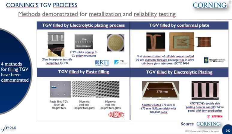
10 PANEL SCALE PACKAGING PLAFORM Key platforms identified to be considered as panel level packaging & manufacturing SUBSTRATE LESS ADVANCED SUBSTRATES FOWLP Silicon Interposer* Glass interposer Organic Interposer Hybrid Interposer Embedded die Key panel level packaging platforms INTERPOSER PLATFORM Embedded interposer EMIB (Intel) EIC (Unimicron) May move to panel Already on panel * Si interposer (2.5D) having fine features (<2/2um) for the high end applications will remain in the wafer format. There are some talks in industry to use the low cost polycrystalline silicon in panel format as the interposer. However, the activities on it are very limited. In this report, Si interposer is not covered in detail and we will give the brief overview of the potential and activities of low cost Si interposer to be used in panel format. 10


11 MOVING TO PANEL BENEFITS Moving to panel: higher economies of scale 695% 500 x500 panel 450% 3906 Moving from wafer to panel format has major cost and productivity advantages due to higher efficiency and economies of scale. 125% 172% 330mm x370 panel 2717 Figures not to scale. for representative purpose only. 100%


12 PANEL TECHNOLOGIES Key packages segments based on panel level integration Organic interposer Glass interposer 5 main available panel technologies for Advanced Packaging Panel Packages FO WLP Panel Hybrid interposer Embedded die Chip Laminated PCB 12


13 APPLICATION TARGETED BY THE PANEL TECHNOLOGY Applications targeted depending on the L/S resolution requirement Application The applications are driving the segmentation of the RDL technology requested FPGA, CPU/GPU, networking, servers RF, Power Management module IC, baseband Mobile, consumer, Wifi, RF, Transducers 2 µm 8 µm 20 µm Line/Space (L/S) 13


 Panel infrastructure Low cost")

14 TECHNICAL GAPS BETWEEN THE WAFER AND PCB INFRASTRUCTURES filled by the panel infrastructure There is a big gap in terms of technical features between the front-end and Back-end/PCB infrastructures Cost between the front-end and PCB areas Gap in terms of cost structure and technical features Front-end technologies Wafer size (300 mm) Panel infrastructure Low cost solution required FO WLP Panel Glass Panel interposer Organic Panel interposer PCB infrastructure 2 µm 5 µm 8 µm Line/Space (L/S) 20 µm 14
15 REVENUE FORECAST FOR PANEL LEVEL PACKAGING In M$ Revenue (in M$) Revenue forecast for panel level packaging (in M$) (Detailed breakdown includes glass panel interposer, embedded die and FO WLP Panel) 450,0 400,0 Yole Developpement November 2015 The panel packaging industry will reach $109M by ,0 300,0 250,0 200,0 150,0 100,0 50,0 0,

16 RESOLUTION TRENDS (L/S: LINE/SPACE): PACKAGING AREA ROADMAP Ready for HVM Ready for initial ramp-up or development Not ready 16

17 Business models PLAYERS POSITIONING INVOLVED IN THE PANEL LEVEL INFRASTRUCTURE Panel Packages Organic interposer Glass interposer Hybrid interposer FOWLP Panel Level Embedded die OSATs * Substrate makers R&D institute IDM * Amkor was actively involved in organic interposer but recently the interest has slowed down 17
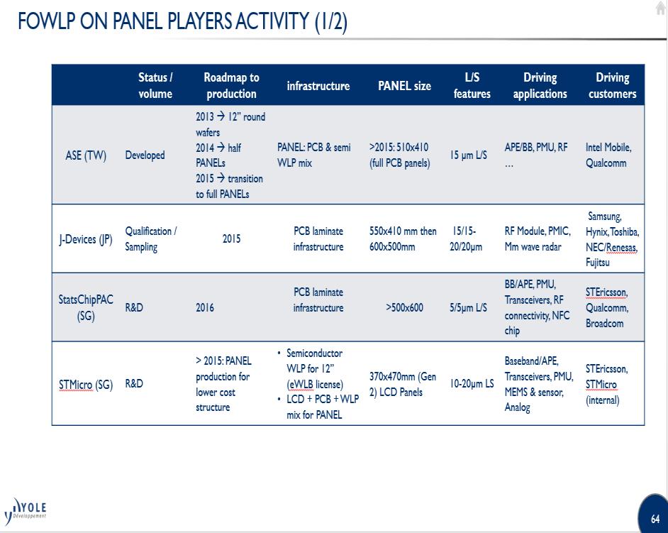
18 PANEL MANUFACTURING ADOPTION Key players pushing the panel manufacturing platform FOWLP on panel Fabless OSATs Substrate makers IDMs Embedded die Glass interposer Organic interposer Hybrid interposer 18


19 OVERVIEW OF EQUIPMENT VENDORS OFFERING TOOLS FOR PANEL PACKAGING Major competitors for Scanner & Laser ablation Major competitors for plating Major competitors for Laser Direct Imaging Major competitors for steppers Major competitors for PVD Major competitors for Pick & Place 19


20 EQUIPMENT LINE INSTALLED ALREADY Type of equipment available of the market Suppliers Panel Packages that can be processed Lithography Glass interposer Organic interposer FO WLP Plating Glass interposer PVD Organic interposer FO WLP 20

21 EQUIPMENT & MATERIALS SUPPLIERS INVOLVED IN THE PANEL INFRASTRUCTURE Embedded die 21


22 MORE SLIDES EXTRACTED 22


23 OUR LATEST REPORTS Coming Soon Coming Soon Coming Soon 23
24 Yole Développement From Technologies to Market 2016

25 FIELDS OF EXPERTISE Yole Développement s 30 analysts operate in the following areas Imaging Photonics MEMS & Sensors MedTech Compound Semi. LED Manufacturing Power Electronics Batteries / Energy Management Advanced Packaging About Yole Développement 25
26 4 BUSINESS MODELS o Consulting and Analysis Market data & research, marketing analysis Technology analysis Strategy consulting Reverse engineering & costing Patent analysis o Financial services M&A (buying and selling) Due diligence Fundraising Maturation of companies IP portfolio management & optimization o Reports o Media Market & Technology reports i-micronews.com website Patent Investigation and patent infringement e-newsletter analysis Communication & webcast services Teardowns & Reverse Costing Analysis Events Cost Simulation Tool


27 A GROUP OF COMPANIES M&A operations Due diligences Market, technology and strategy consulting Fundraising Maturation of companies IP portfolio management & optimization Manufacturing costs analysis Teardown and reverse engineering Cost simulation tools IP analysis Patent assessment 27

28 OUR GLOBAL ACTIVITY 28


29 SERVING THE ENTIRE SUPPLY CHAIN Integrators and end-users Our analysts provide market analysis, technology evaluation, and business plan along the entire supply chain Device makers Suppliers: material, equipment, OSAT, foundries Financial investors, R&D centers 29

30 CONTACT INFORMATION Consulting and Specific Analysis North America: Steve LaFerriere, Director of Northern America Business Development Japan: Yutaka Katano, General Manager, Yole Japan & President, Yole K.K. RoW: Jean-Christophe Eloy, CEO & President, Yole Développement Report business North America: Steve LaFerriere, Director of Northern America Business Development Europe: Fayçal El Khamassi, Headquarter Sales Coordination & Customer Service Japan & Asia: Takashi Onozawa, Sales Asia & General Manager, Yole K.K. Korea: Hailey Yang, Business Development Manager, Korean Office Follow us on Financial services Jean-Christophe Eloy, CEO & President General 30
Glass Substrates for Semiconductor Manufacturing
 Glass Substrates for Semiconductor Manufacturing The first REPORT analyzing in detail the glass wafer for wafer level packaging and micro structuring technologies applications 2013 Content of the report
Yole Developpement. Developpement-v2585/ Publisher Sample
 Yole Developpement http://www.marketresearch.com/yole- Developpement-v2585/ Publisher Sample Phone: 800.298.5699 (US) or +1.240.747.3093 or +1.240.747.3093 (Int'l) Hours: Monday - Thursday: 5:30am - 6:30pm
Photolithography for Advanced Packaging, MEMS & LEDs
 From Technologies to Market Photolithography for Advanced Packaging, MEMS & LEDs Report June 2015 ABOUT THE AUTHORS Biography & contact Amandine PIZZAGALLI, Market & Technology Analyst, Equipment and Materials
Photonique sur silicium: Tendances et perspectives de marché
 From Technologies to Market Photonique sur silicium: Tendances et perspectives de marché Eric MOUNIER, YOLE DEVELOPPEMENT 2017 FIELDS OF EXPERTISE Yole Développement s 30 analysts operate in the following
Fan-Out Wafer Level Packaging Patent Landscape Analysis
 Fan-Out Wafer Level Packaging Patent Landscape Analysis Source: Infineon Source: TSMC Source: ASE November 2016 Source: Deca Technologies Source: STATS ChipPAC Source: Nepes KnowMade Patent & Technology
Fan-Out Wafer Level Packaging Patent Landscape Analysis
 Fan-Out Wafer Level Packaging Patent Landscape Analysis Source: Infineon Source: TSMC Source: ASE November 2016 Source: Deca Technologies Source: STATS ChipPAC Source: Nepes KnowMade Patent & Technology
From Technologies to Market. Laser Technologies for. Semiconductor. Manufacturing. Sample. October 2017
 From Technologies to Market Laser Technologies for Semiconductor Manufacturing Sample October 2017 REPORT OBJECTIVES This report is the first research performed on the laser technologies in the field of
Consumer Physics SCiO Molecular Sensor
 Consumer Physics SCiO Molecular Sensor Pocket handheld spectrometer MEMS/Imaging report by Stéphane ELISABETH February 2017 21 rue la Noue Bras de Fer 44200 NANTES - FRANCE +33 2 40 18 09 16 info@systemplus.fr
TechSearch International, Inc. Corporate Overview E. Jan Vardaman, President
 TechSearch International, Inc. Corporate Overview E. Jan Vardaman, President Corporate Background Founded in 1987 and headquartered in Austin, Texas Recognized around the world as a leading consulting
Autoliv Night Vision System Safety Application Automotive IR Camera
 Autoliv Night Vision System Safety Application Automotive IR Camera Report by Farid HAMRANI & Sylvain HALLEREAU June 2017 21 rue la Noue Bras de Fer 44200 NANTES - FRANCE +33 2 40 18 09 16 info@systemplus.fr
The Future of Packaging ~ Advanced System Integration
 The Future of Packaging ~ Advanced System Integration Enabling a Microelectronic World R. Huemoeller SVP, Adv. Product / Platform Develop June 2013 Product Segments End Market % Share Summary 2 New Product
GaN Power Epitaxy, Devices, Applications and Technology Trends
 From Technologies to Market GaN Power Epitaxy, Devices, Applications and Technology Trends Sample October 2017 Biographies & contacts Dr. Ana Villamor Dr Ana Villamor serves as a Technology & Market Analyst
Semiconductor and LED Markets. Jon Sabol Vice President and General Manager Semiconductor and LED Division
 Semiconductor and LED Markets Jon Sabol Vice President and General Manager Semiconductor and LED Division Semiconductor & LED Investing in Semiconductor and LED $ Millions 300 200 27% CAGR 100 0 * FY06
Disruptive Developments for Advanced Die Attach to Tackle the Challenges of Heterogeneous Integration
 Disruptive Developments for Advanced Die Attach to Tackle the Challenges of Heterogeneous Integration Hugo Pristauz & Andreas Mayr, Besi Austria presented by: Stefan Behler, Besi Switzerland ECTC 2018
From Technologies to Market. LED Lighting Module. Technology, Industry. and Market Trends. Sample. Market & Technology Report
 From Technologies to Market LED Lighting Module Technology, Industry and Market Trends Sample Market & Technology Report TABLE OF CONTENT OF THE REPORT (1/4) o Authors of the Report P6 o Objectives of
FOR IMMEDIATE RELEASE. Yole s analysts believe in a wide adoption of gas sensors in consumer products
 FOR IMMEDIATE RELEASE Yole s analysts believe in a wide adoption of gas sensors in consumer products Gas Sensor Technology & Market report, February 2016 LYON, France February 11, 2016: The latest analysis
From Technologies to Market. Advanced RF SiP for Cell Phones
 From Technologies to Market Advanced RF SiP for Cell Phones 2017 2017 REPORT METHODOLOGY Market forecast methodology Market segmentation methodology 2017 www.yole.fr Advanced RF SiP for Cell Phones 2017
STMicroelectronics ToF Proximity Sensor & Flood Illuminator in the Apple iphone X
 STMicroelectronics ToF Proximity Sensor & Flood Illuminator in the Apple iphone X Patent-to-Product Mapping August 2018 KnowMade Patent & Technology Intelligence 2018 www.knowmade.com TABLE OF CONTENTS
SUSS MICROTEC INVESTOR PRESENTATION. February 2014
 SUSS MICROTEC INVESTOR PRESENTATION February 2014 DISCLAIMER This presentation contains forward-looking statements relating to the business, financial performance and earnings of SUSS MicroTec AG and its
SiP packaging technology of intelligent sensor module. Tony li
 SiP packaging technology of intelligent sensor module Tony li 2016.9 Contents What we can do with sensors Sensor market trend Challenges of sensor packaging SiP technology to overcome challenges Overview
Apple iphone X IR Dot Projector
 Apple iphone X IR Dot Projector Dot Projector bundle including Heptagon Imaging report by Sylvain HALLEREAU December 2017 21 rue la Noue Bras de Fer 44200 NANTES - FRANCE +33 2 40 18 09 16 info@systemplus.fr
ams Multi-Spectral Sensor True Color ambient light sensor from Apple iphone X
 ams Multi-Spectral Sensor True Color ambient light sensor from Apple iphone X IMAGING report by Stéphane ELISABETH December 2017 version 1 21 rue la Noue Bras de Fer 44200 NANTES - FRANCE +33 2 40 18 09
POSSUM TM Die Design as a Low Cost 3D Packaging Alternative
 POSSUM TM Die Design as a Low Cost 3D Packaging Alternative The trend toward 3D system integration in a small form factor has accelerated even more with the introduction of smartphones and tablets. Integration
Uncooled Infrared Imagers Technology & Market Trends 2017
 From Technologies to Market Uncooled Infrared Imagers Technology & Market Trends 2017 Sample August 2017 TABLE OF CONTENTS Glossary, definitions, scope & report objectives 4 Executive summary 9 Introduction
EMERGING SUBSTRATE TECHNOLOGIES FOR PACKAGING
 EMERGING SUBSTRATE TECHNOLOGIES FOR PACKAGING Henry H. Utsunomiya Interconnection Technologies, Inc. Suwa City, Nagano Prefecture, Japan henryutsunomiya@mac.com ABSTRACT This presentation will outline
MICRONEWS MEDIA
 www.i-micronews.com MICRONEWS MEDIA 2013 MediA Kit www.i-micronews.com "Yole Développement has a deep understanding of various technologies, and accounts for all economic parameters in its studies. Our
Lithography in our Connected World
 Lithography in our Connected World SEMI Austin Spring Forum TOP PAN P R INTING CO., LTD MATER IAL SOLUTIONS DIVISION Toppan Printing Co., LTD A Broad-Based Global Printing Company Foundation: January 17,
Organic Packaging Substrate Workshop Overview
 Organic Packaging Substrate Workshop Overview Organized by: International Electronics Manufacturing Initiative (inemi) Mario A. Bolanos November 17-18, 2009 1 Organic Packaging Substrate Workshop Work
The Development of the Semiconductor CVD and ALD Requirement
 The Development of the Semiconductor CVD and ALD Requirement 1 Linx Consulting 1. We create knowledge and develop unique insights at the intersection of electronic thin film processes and the chemicals
Recent Developments in Multifunctional Integration. Stephan Guttowski, Head of Technology Park»Heterointegration«, Fraunhofer FMD
 Recent Developments in Multifunctional Integration Stephan Guttowski, Head of Technology Park»Heterointegration«, Fraunhofer FMD Founding Participants 2 One-Stop-Shop for developments from wafer technologies
Fraunhofer IZM - ASSID
 FRAUNHOFER-INSTITUT FÜR Zuverlässigkeit und Mikrointegration IZM Fraunhofer IZM - ASSID All Silicon System Integration Dresden Heterogeneous 3D Wafer Level System Integration 3D system integration is one
New Wave SiP solution for Power
 New Wave SiP solution for Power Vincent Lin Corporate R&D ASE Group APEC March 7 th, 2018 in San Antonio, Texas. 0 Outline Challenges Facing Human Society Energy, Environment and Traffic Autonomous Driving
First Demonstration of Panel Glass Fan-out (GFO) Packages for High I/O Density and High Frequency Multi-Chip Integration
 Packages for High I/O Density and High Frequency Multi-Chip Integration") First Demonstration of Panel Glass Fan-out (GFO) Packages for High I/O Density and High Frequency Multi-Chip Integration Tailong Shi, Chintan Buch,Vanessa Smet, Yoichiro Sato, Lutz Parthier, Frank Wei
First Demonstration of Panel Glass Fan-out (GFO) Packages for High I/O Density and High Frequency Multi-Chip Integration Tailong Shi, Chintan Buch,Vanessa Smet, Yoichiro Sato, Lutz Parthier, Frank Wei
450mm patterning out of darkness Backend Process Exposure Tool SOKUDO Lithography Breakfast Forum July 10, 2013 Doug Shelton Canon USA Inc.
 450mm patterning out of darkness Backend Process Exposure Tool SOKUDO Lithography Breakfast Forum 2013 July 10, 2013 Doug Shelton Canon USA Inc. Introduction Half Pitch [nm] 2013 2014 2015 2016 2017 2018
HTC Vive VR (Model 0PJT100) Virtual Reality Headset
 Virtual Reality Headset") HTC Vive VR (Model 0PJT100) Virtual Reality Headset System report by Wilfried THERON February 2017 21 rue la Noue Bras de Fer 44200 NANTES - FRANCE +33 2 40 18 09 16 info@systemplus.fr www.systemplus.fr
HTC Vive VR (Model 0PJT100) Virtual Reality Headset System report by Wilfried THERON February 2017 21 rue la Noue Bras de Fer 44200 NANTES - FRANCE +33 2 40 18 09 16 info@systemplus.fr www.systemplus.fr
3D ICs: Recent Advances in the Industry
 3D ICs: Recent Advances in the Industry Suresh Ramalingam Senior Director, Advanced Packaging Outline 3D IC Background 3D IC Technology Development Summary Acknowledgements Stacked Silicon Interconnect
Packaging Roadmap: The impact of miniaturization. Bob Pfahl, inemi Celestica-iNEMI Technology Forum May 15, 2007
 Packaging Roadmap: The impact of miniaturization Bob Pfahl, inemi Celestica-iNEMI Technology Forum May 15, 2007 The Challenges for the Next Decade Addressing the consumer experience using the converged
WLP Probing Technology Opportunity and Challenge. Clark Liu
 WLP Probing Technology Opportunity and Challenge Founded Capital PTI Group Overview : May/15/97 : USD 246 Millions PTI HQ Total Assets : USD 2.2B Employees Major Services : 11,100 (Greatek included) :
Noel Technologies. Provider of Advanced Lithography and Semiconductor Thin Film Services
 Noel Technologies Provider of Advanced Lithography and Semiconductor Thin Film Services Noel Technologies Keith Best Biography Over the last 27 years, Keith Best has held a variety of semiconductor processing
Market and technology trends in advanced packaging
 Close Market and technology trends in advanced packaging Executive OVERVIEW Recent advances in device miniaturization trends have placed stringent requirements for all aspects of product manufacturing.
RF GaN Market. Applications, players, devices, and technologies
 RF GaN Market Applications, players, devices, and technologies 2018 2023 RF GaN Market Sample www.yole.fr 2018 REPORT OBJECTIVES Provide an overview of the RF GaN market. Analyze different players in different
Flexline - A Flexible Manufacturing Method for Wafer Level Packages (Extended Abstract)
") Flexline - A Flexible Manufacturing Method for Wafer Level Packages (Extended Abstract) by Tom Strothmann, *Damien Pricolo, **Seung Wook Yoon, **Yaojian Lin STATS ChipPAC Inc.1711 W Greentree Drive Tempe,
Flexline - A Flexible Manufacturing Method for Wafer Level Packages (Extended Abstract) by Tom Strothmann, *Damien Pricolo, **Seung Wook Yoon, **Yaojian Lin STATS ChipPAC Inc.1711 W Greentree Drive Tempe,
Application-Based Opportunities for Reused Fab Lines
 Application-Based Opportunities for Reused Fab Lines Semicon China, March 17 th 2010 Keith Best Simax Lithography S I M A X A L L I A N C E P A R T N E R S Outline Market: Exciting More than Moore applications
EPTC 2017 Panel Session Packaging Challenges & Opportunities of 5G-mm Wave Technology
 EPTC 2017 Panel Session Packaging Challenges & Opportunities of 5G-mm Wave Technology Moderator : Dr. Rick Sturdivant, Department of Engineering and Computer Science, Azusa Pacific University, USA. Dr.
The SEMATECH Model: Potential Applications to PV
 Continually cited as the model for a successful industry/government consortium Accelerating the next technology revolution The SEMATECH Model: Potential Applications to PV Dr. Michael R. Polcari President
Min Tao, Ph. D, Ashok Prabhu, Akash Agrawal, Ilyas Mohammed, Ph. D, Bel Haba, Ph. D Oct , IWLPC
 PACKAGE-ON-PACKAGE INTERCONNECT FOR FAN-OUT WAFER LEVEL PACKAGES Min Tao, Ph. D, Ashok Prabhu, Akash Agrawal, Ilyas Mohammed, Ph. D, Bel Haba, Ph. D Oct 18-20 2016, IWLPC 1 Outline Laminate to Fan-Out
Accelerating Growth and Cost Reduction in the PV Industry
 Accelerating Growth and Cost Reduction in the PV Industry PV Technology Roadmaps and Industry Standards An Association s Approach Bettina Weiss / SEMI PV Group July 29, 2009 SEMI : The Global Association
450mm and Moore s Law Advanced Packaging Challenges and the Impact of 3D
 450mm and Moore s Law Advanced Packaging Challenges and the Impact of 3D Doug Anberg VP, Technical Marketing Ultratech SOKUDO Lithography Breakfast Forum July 10, 2013 Agenda Next Generation Technology
SEMI Connects: An Overview of SEMI Worldwide. Theresia Fasinski - Manager Membership Relations, SEMI Europe
 SEMI Connects: An Overview of SEMI Worldwide Theresia Fasinski - Manager Membership Relations, SEMI Europe SEMI Connects to Advance a Global Industry Mission SEMI provides industry stewardship and engages
Innovations Push Package-on-Package Into New Markets. Flynn Carson. STATS ChipPAC Inc Kato Rd Fremont, CA 94538
 Innovations Push Package-on-Package Into New Markets by Flynn Carson STATS ChipPAC Inc. 47400 Kato Rd Fremont, CA 94538 Copyright 2010. Reprinted from Semiconductor International, April 2010. By choosing
Laminate Based Fan-Out Embedded Die Technologies: The Other Option
 Laminate Based Fan-Out Embedded Die Technologies: The Other Option Theodore (Ted) G. Tessier, Tanja Karila*, Tuomas Waris*, Mark Dhaenens and David Clark FlipChip International, LLC 3701 E University Drive
MEDIA RELEASE FOR IMMEDIATE RELEASE. 8 November 2017
 MEDIA RELEASE FOR IMMEDIATE RELEASE 8 November 2017 A*STAR IME S NEW MULTI-CHIP FAN-OUT WAFER LEVEL PACKAGING DEVELOPMENT LINE TO DRIVE INNOVATION AND GROWTH IN SEMICONDUCTOR INDUSTRY State-of-the-art
MEDIA RELEASE FOR IMMEDIATE RELEASE 26 JULY 2016
 MEDIA RELEASE FOR IMMEDIATE RELEASE 26 JULY 2016 A*STAR S IME KICKS OFF CONSORTIA TO DEVELOP ADVANCED PACKAGING SOLUTIONS FOR NEXT-GENERATION INTERNET OF THINGS APPLICATIONS AND HIGH-PERFORMANCE WIRELESS
15 APRIL 2015 A*STAR S IME SMART DEVICES. capabilities. Semiconductors, Technologies, multi-functional. Page 1 of
 MEDIA RELEASE FOR IMMEDIATE RELEASE 15 APRIL 2015 A*STAR S IME AND INDUSTRY PARTNERS TO ENABLE HIGH DENSITY / LOW-COST PACKAGINGG TECHNOLOGY FOR SYSTEM SCALING WITHIN SMART DEVICES New capabilities in
Phoenix Semiconductor Philippines Corp (PSPC) to be listed on December 1, Semiconductor historical billings report in 000 US$
 to be listed on December 1, Semiconductor historical billings report in 000 US$") Report date: November 10, 2014 Phoenix Semiconductor Philippines Corp (PSPC) to be listed on December 1, 2014 Recommendation: Cautious buy with target price of Php 3.81/share At the final offer price of
Report date: November 10, 2014 Phoenix Semiconductor Philippines Corp (PSPC) to be listed on December 1, 2014 Recommendation: Cautious buy with target price of Php 3.81/share At the final offer price of
Growing the Semiconductor Industry in New York: Challenges and Opportunities
 Accelerating the next technology revolution The SEMATECH New York Experience Growing the Semiconductor Industry in New York: Challenges and Opportunities Dan Armbrust President and CEO, SEMATECH April
The Collaboration Engine: Enabling Innovation in Microelectronics
 The Collaboration Engine: Enabling Innovation in Microelectronics Karen Savala President, SEMI Americas Outline About SEMI Semiconductors: A History of Collaboration Collaboration in other Microelectronics
Electronic Costing & Technology Experts
 Electronic Costing & Technology Experts 21 rue la Nouë Bras de Fer 44200 Nantes France Phone : +33 (0) 240 180 916 email : info@systemplus.fr www.systemplus.fr September 2016 Version 1 Written by Stéphane
TSV MEOL (Mid-End-Of-Line) and its Assembly/Packaging Technology for 3D/2.5D Solutions
 and its Assembly/Packaging Technology for 3D/2.5D Solutions") TSV MEOL (Mid-End-Of-Line) and its Assembly/Packaging Technology for 3D/2.5D Solutions Seung Wook YOON, D.J. Na, *K. T. Kang, W. K. Choi, C.B. Yong, *Y.C. Kim and Pandi C. Marimuthu STATS ChipPAC Ltd.
TSV MEOL (Mid-End-Of-Line) and its Assembly/Packaging Technology for 3D/2.5D Solutions Seung Wook YOON, D.J. Na, *K. T. Kang, W. K. Choi, C.B. Yong, *Y.C. Kim and Pandi C. Marimuthu STATS ChipPAC Ltd.
THE WAFER FAB CLEANS IN SEMICONDUCTOR INDUSTRY FROM A MATERIALS SUPPLIER PERSPECTIVE
 THE WAFER FAB CLEANS IN SEMICONDUCTOR INDUSTRY FROM A MATERIALS SUPPLIER PERSPECTIVE Tianniu Rick Chen, Ph.D. General Manager SP&C Business (Surface Preparation & Cleans) OUTLINE Market drivers and challenges
Session 4: Mixed Signal RF
 Sophia Antipolis October 5 th & 6 th 2005 Session 4: Mixed Signal RF Technology, Design and Manufacture of RF SiP Chris Barratt, Michel Beghin, Insight SiP Insight SiP Summary Introduction Definition of
Silicon Photonics Transceivers for Hyper Scale Datacenters: Deployment and Roadmap
 Silicon Photonics Transceivers for Hyper Scale Datacenters: Deployment and Roadmap Peter De Dobbelaere Luxtera Inc. 09/19/2016 Luxtera Proprietary www.luxtera.com Luxtera Company Introduction $100B+ Shift
inemi Substrate & Packaging Technology Workshop
 Presentation Program (April 22, 2014) 08:15 Welcome tea and coffee 08:30 Welcome and Workshop introduction Bill Bader, inemi CEO 09:00 09:45 Current Technologies and Future Developments in Advanced Packaging
Proceedings. BiTS Shanghai October 21, Archive - Session BiTS Workshop Image: Zhu Difeng/Dollar Photo Club
 Proceedings Archive - Session 2 2015 BiTS Workshop Image: Zhu Difeng/Dollar Photo Club Proceedings With Thanks to Our Sponsors! Premier Honored Distinguished Publication Sponsor 2 Proceedings Presentation
Photoresists & Ancillaries. Materials for Semiconductor Manufacturing A TECHCET Critical Materials Report
 2018-19 Photoresists & Ancillaries Materials for Semiconductor Manufacturing A TECHCET Critical Materials Report Prepared by Ed Korczynski Reviewed and Edited by Lita Shon-Roy TECHCET CA LLC PO Box 3814
2016 IEEE 66th Electronic Components and Technology Conference
 2016 IEEE 66th Electronic Components and Technology Conference Next Generation Panel-Scale RDL with Ultra Small Photo Vias and Ultra-fine Embedded Trenches for Low Cost 2.5D Interposers and High Density
"All in one Package The Packaging Solution of the Future?
 "All in one Package The Packaging Solution of the Future? Rainbow Yuan, AT&S SIP China 2017 AT&S (China) Company Limited 奥特斯 ( 中国 ) 有限公司 No.5000 Jin Du Road Xinzhuang Industry Park Shanghai 201108 P.R.
Advanced Wafer Level Packaging of RF-MEMS with RDL Inductor
 Advanced Wafer Level Packaging of RF-MEMS with RDL Inductor Paul Castillou, Roberto Gaddi, Rob van Kampen, Yaojian Lin*, Babak Jamshidi** and Seung Wook Yoon*** Cavendish Kinetics, 2960 North First Street,
Camera Module Industry 2017
 From Technologies to Market Camera Module Industry 2017 Sample November 2017 ABOUT THE AUTHORS OF THIS REPORT Biography & contact Pierre Cambou Pierre Cambou joined the imaging industry in 1999. Following
Technology Transfers Opportunities, Process and Risk Mitigation. Radhika Srinivasan, Ph.D. IBM
 Technology Transfers Opportunities, Process and Risk Mitigation Radhika Srinivasan, Ph.D. IBM Abstract Technology Transfer is quintessential to any technology installation or semiconductor fab bring up.
Trends in Advanced Packaging Technologies An IMAPS UK view
 Trends in Advanced Packaging Technologies An IMAPS UK view Andy Longford Chair IMAPS UK 2007 9 PandA Europe IMAPS UK IeMRC Interconnection event December 2008 1 International Microelectronics And Packaging
2010 IRI Annual Meeting R&D in Transition
 2010 IRI Annual Meeting R&D in Transition U.S. Semiconductor R&D in Transition Dr. Peter J. Zdebel Senior VP and CTO ON Semiconductor May 4, 2010 Some Semiconductor Industry Facts Founded in the U.S. approximately
A Low-cost Through Via Interconnection for ISM WLP
 A Low-cost Through Via Interconnection for ISM WLP Jingli Yuan, Won-Kyu Jeung, Chang-Hyun Lim, Seung-Wook Park, Young-Do Kweon, Sung Yi To cite this version: Jingli Yuan, Won-Kyu Jeung, Chang-Hyun Lim,
Update: SOI Wafer Market Continues Its Growth
 Gartner Dataquest Alert Update: SOI Wafer Market Continues Its Growth The results of Gartner Dataquest's latest survey of the silicon on insulator (SOI) wafer market indicate demand grew 16 percent in
LED Lighting Module Technology Industry and Market Trends
 From Technologies to Market LED Lighting Module Technology Industry and Market Trends Sample September 2017 TABLE OF CONTENT (1/6) o ACRONYM P8 o OBJECTIVES OF THE REPORT P9 o AUTHORS OF THE REPORT P10
Knowles MEMS Microphones in Apple iphone 7 Plus
 Knowles MEMS Microphones in Apple iphone 7 Plus Patent-to-Product Mapping March 2017 KnowMade Patent & Technology Intelligence 2017 www.knowmade.com TABLE OF CONTENTS INTRODUCTION 6 Company profile 7 Scope
2D to 3d architectures: back to the future
 2D to 3d architectures: back to the future Raja Swaminathan Package architect Intel Corporation 2018 IMAPS Device Packaging Keynote, 03/06/2018 acknowledgements Ravi Mahajan, Ram Viswanath, Bob Sankman,
Silicon Interposers enable high performance capacitors
 Interposers between ICs and package substrates that contain thin film capacitors have been used previously in order to improve circuit performance. However, with the interconnect inductance due to wire
ASML Market dynamics. Dave Chavoustie EVP Sales Analyst Day, September 30, 2004
 ASML Market dynamics Dave Chavoustie EVP Sales Analyst Day, September 30, 2004 Agenda! Market Overview! Growth Opportunities! 300mm Market! Asia Overview / Slide 2 ASML Unit Market Share Trend 60% 12 &
Integrated Photonics using the POET Optical InterposerTM Platform
 Integrated Photonics using the POET Optical InterposerTM Platform Dr. Suresh Venkatesan CIOE Conference Shenzhen, China Sept. 5, 2018 POET Technologies Inc. TSXV: PUBLIC POET PTK.V Technologies Inc. PUBLIC
Markets for On-Chip and Chip-to-Chip Optical Interconnects 2015 to 2024 January 2015
 Markets for On-Chip and Chip-to-Chip Optical Interconnects 2015 to 2024 January 2015 Chapter One: Introduction Page 1 1.1 Background to this Report CIR s last report on the chip-level optical interconnect
Embedded Image and Vision Processing
 From Technologies to Market Embedded Image and Vision Processing Sample November 2017 ABOUT THE AUTHORS Biographies and Contacts Yohann Tschudi As a Software & Market Analyst, Dr. Yohann Tschudi is a member
David B. Miller Vice President & General Manager September 28, 2005
 Electronic Technologies Business Overview David B. Miller Vice President & General Manager September 28, 2005 Forward Looking Statement During the course of this meeting we may make forward-looking statements.
GLOBAL MARKETS, TECHNOLOGIES AND MATERIALS FOR THIN AND ULTRATHIN FILMS
 GLOBAL MARKETS, TECHNOLOGIES AND MATERIALS FOR THIN AND ULTRATHIN FILMS SMC057C August Margareth Gagliardi Project Analyst ISBN: 1-62296-338-5 BCC Research 49 Walnut Park, Building 2 Wellesley, MA 02481
IMPACT OF 450MM ON CMP
 IMPACT OF 450MM ON CMP MICHAEL CORBETT MANAGING PARTNER LINX CONSULTING, LLC MCORBETT@LINX-CONSULTING.COM PREPARED FOR CMPUG JULY 2011 LINX CONSULTING Outline 1. Overview of Linx Consulting 2. CMP Outlook/Drivers
Thermal Management in the 3D-SiP World of the Future
 Thermal Management in the 3D-SiP World of the Future Presented by W. R. Bottoms March 181 th, 2013 Smaller, More Powerful Portable Devices Are Driving Up Power Density Power (both power delivery and power
Smart Devices of 2025
 Smart Devices of 2025 Challenges for Packaging of Future Device Technologies Steve Riches/Kevin Cannon Tribus-D Ltd CW Workshop 27 March 2018 E:mail: info@tribus-d.uk M: 07804 980 954 Assembly Technology
Advanced Packaging Solutions
 Advanced Packaging Solutions by USHIO INC. USHIO s UX Series Providing Advanced Packaging Solutions Page 2 USHIO s UX Series Models Featured @ SEMICON West 2013 Page 2 Large-Size Interposer Stepper UX7-3Di
Opportunities and challenges of silicon photonics based System-In-Package
 Opportunities and challenges of silicon photonics based System-In-Package ECTC 2014 Panel session : Emerging Technologies and Market Trends of Silicon Photonics Speaker : Stéphane Bernabé (Leti Photonics
Newsletter no. 01 / Nov. 2009
 www.hermes-ect.net Newsletter no. 01 / Nov. 2009 Content Issue No. 1: I. Why chip embedding? II. Objectives & aims III. Supply chain IV. Building up the business V. Embedded applications in HERMES HERMES
Electronic Costing & Technology Experts
 Electronic Costing & Technology Experts 21 rue la Nouë Bras de Fer 44200 Nantes France Phone : +33 (0) 240 180 916 email : info@systemplus.fr www.systemplus.fr October 2016 Preliminary Version Written
LED Cost and Technology Trends: How to enable massive adoption in general lighting
 LED Cost and Technology Trends: How to enable massive adoption in general lighting SEMICON West 2011 Moscone Center, San Francisco June 13 th 2011 Lumileds Lumileds OSRAM Aixtron CREE OSRAM OKI OSRAM 45
MEPTEC Roadmaps 2013 Session 1 Notes. Paul Werbaneth 3D InCites
 MEPTEC Roadmaps 2013 Session 1 Notes Paul Werbaneth 3D InCites www.3dincites.com Session 1: Product Drivers Panel Moderator: Joel Camarda, Amonix Panelists: Mudasir Ahmad, Cisco Farshad Ghahghahi, LSI
Image Sensor Advanced Package Solution. Prepared by : JL Huang & KingPak RD division
 Image Sensor Advanced Package Solution Prepared by : JL Huang & KingPak RD division Contents CMOS image sensor marketing overview Comparison between different type of CMOS image sensor package Overview
Technology for the MEMS processing and testing environment. SUSS MicroTec AG Dr. Hans-Georg Kapitza
 Technology for the MEMS processing and testing environment SUSS MicroTec AG Dr. Hans-Georg Kapitza 1 SUSS MicroTec Industrial Group Founded 1949 as Karl Süss KG GmbH&Co. in Garching/ Munich San Jose Waterbury
EUFANET. Full Wafer Level Stacking without TSV Applications to Memory-only and heterogeneous SiP
 EUFANET Full Wafer Level Stacking without TSV Applications to Memory-only and heterogeneous SiP Presented by Dr Christian Val Co-founder and CEO of 3D Plus 408 rue Hélène Boucher 78532 BUC (France) cval@3d-plus.com
A Perspective on Semiconductor Equipment. R. B. Herring March 4, 2004
 A Perspective on Semiconductor Equipment R. B. Herring March 4, 2004 Outline Semiconductor Industry Overview of circuit fabrication Semiconductor Equipment Industry Some equipment business strategies Product
DIGITAL POWER ICs High Growth Opportunities for IC and Foundry Vendors
 DIGITAL POWER ICs High Growth Opportunities for IC and Foundry Vendors ABSTRACT The purpose of this report is to deliver an up-to-date understanding of the digital power IC market landscape from five major
Advanced Stepper Lithography Technology to Enable Flexible AMOLED Displays. Keith Best Roger McCleary Elvino M da Silveira 5/19/17
 Advanced Stepper Lithography Technology to Enable Flexible AMOLED Displays Keith Best Roger McCleary Elvino M da Silveira 5/19/17 Agenda About Rudolph JetStep G System overview and performance Display
Display Materials and Components Report - Glass Slimming 2013
 Display Materials and Components Report - Glass Slimming 2013 May 2013 Doo.Kim@ihs.com www.displaybank.com 1/130 No material contained in this report may be reproduced in whole or in part without the express