LED Cost and Technology Trends: How to enable massive adoption in general lighting
|
|
|
- Stanley O’Neal’
- 6 years ago
- Views:
Transcription


1 LED Cost and Technology Trends: How to enable massive adoption in general lighting SEMICON West 2011 Moscone Center, San Francisco June 13 th 2011 Lumileds Lumileds OSRAM Aixtron CREE OSRAM OKI OSRAM 45 rue Sainte Geneviève, F Lyon, France Tel: Fax: Web:
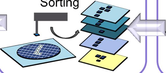
2 Content Rationale: why are cost reductions necessary? LED die singulation. Packaging substrates Conclusion


3 Packaged LED: Revenue by Application (Base Scenario) Sources: Yole Développement? General Lighting to take off only if cost/performance can beat incumbent technologies


4 Upfront Cost: Sticker Shock: All sources: ~ 800 lumens Warm White Tier 1 brand <$1 $3-5 $40 Need to reduce $/lumen!


5 Cumulated Cost of Light = Upfront Cost + Energy Cost + Maintenance Cost

6 Cumulated Cost: Examples Standard A19 Warm white Bulb 800 lumen No maintenance cost (residential use) Sources: Yole Développement $40 LED Bulb: LED cumulated cost remains higher than Fluorescent light sources


7 Cumulated Cost: Examples Sources: Yole Développement $10 LED Bulb: LED becomes significantly cheaper than other light source + upfront cost more acceptable trigger for massive market adoption
8 The Path to Cost Reduction Cost = $/Lumen Manufacturing Efficiency: Higher equipment throughput Higher yields Economy of scale LED performance: Higher Efficiency (lumen/w) More light per chip
9 20 Key Technologies & Research Areas Relative Impact on LED cost of ownership Manufacturing Cost Alternative substrates #2: Si Large Diameters Substrates: 4, 6, 8 Lithography: Dedicated tools, Higher Throughput Testing and Binning: Wafer Level, Higher throughputs Die Singulation Increased throughputs and yields Contacts/Electrodes: Transparent contacts/electrode materials and patterns Encapsulation Materials and Optics: Ageing and optical properties Contacts & Electrodes: p to n layer VIAS Epitaxy: Cluster tools - New Epi Technologies Substrate Separation: Laser Lift Off, other separation techniques Wafer Level Packaging: Silicon TSV, Wafer Level Optics Phosphors: Conversion efficiency, Color Rendering IP free phosphors Mirrors: Resonant Cavities Mirrors: Improve reflectivity/electrical properties Surface Texturation: Patterned substrates / Roughening Epitaxy MOCVD: Higher yields and Throughputs - Improved Material quality Phosphors: Quantum dots Phosphors Alternative substrates #1: GaN, ZnO, Si, Engineered substrates Thermal Management: New materials for packaging Surface Texturation: Photonic and Quasi Photonic Crystals Current Droop / Green Gap / LED Structures Sources: Yole Développement LED Performance


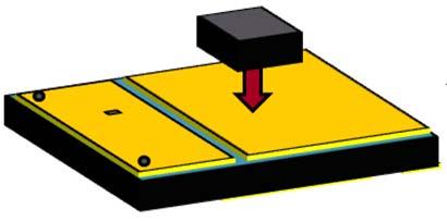
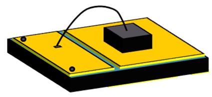
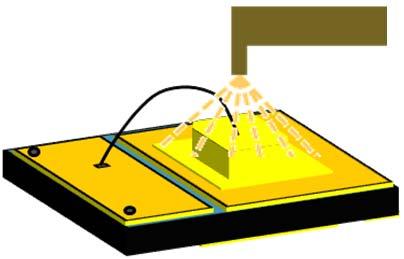
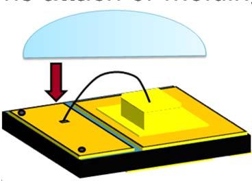
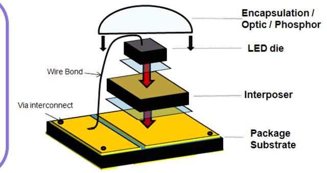
10 Typical Process Flow: Carrier wafer Carrier wafer Epitaxial substrate Epiwafer Die Lens Each step represents an opportunity for cost improvement


11 Typical Process Flow: Die

 Blade Dicing 2)")


12 LED Singulation: 4 different processes can be used for LED die singulation: Dicing Process 1) Blade Dicing 2) Laser Dicing LED Epiwafer 3) Diamond Scribing Breaking Scribe & Break 4) Laser Scribing Scribed Epiwafer LED dice


13 Critical Parameters: Dicing and LED Cost Reducing street width increase die/wafers count. Cutting speed increase equipment throughput Cutting yields good die per wafers Performance some processes reduce brightness: lower die value Street Width Scribing Depth Kerf Loss Picture: JPSA Picture: JPSA Picture: A.L.S.I


14 Improving Throughput: Main Factors influencing Dicing Speed: Materials: GaN Sapphire GaAs SiC Si, Ge Cu, CuW, Mo Scribing depth: Indexing speed: Vertical LED chip bonded on metal substrate Scribe depth versus scribe speed for a 266nm laser using 1W average power at 30kHz (source: Oxford Lasers) Recasting effect on metal after laser scribing Trade off between speed and depth Indexing / alignment times are critical to throughput


15 Increasing Speed (1): Serial Multibeam Laser Dicing Increasing laser dicing speed requires higher laser energy: damages the components. Solution: Serial Multibeams Expander Diffractive Optical Element Laser Beams Multibeam vs. high energy single beam (right) beam splitting technique (ALSI) Wafer 1 st pulse n th pulse Side view of a 650 um thick GaAs wafer scribed with a mutibeam laser (ALSI) Illustration of Multibeam laser dicing process (source: ALSI)

 Wafer/ hour 50 100 150 300 x2 9 13 15 18 Increase factor 6 5 4 3 2 1 Speed increase")


16 Increasing Speed (2): Parallel cuts Comparison of wafer throughput vs. scribing speed: Hypothesis: 2 wafer, 350 um die, 20 um x6street width. 7 Results: a 6x speed increase would lead to a 2x improvement in wafer throughput: Speed (mm/s) Wafer/ hour x Increase factor Speed increase Wafer Throughput increase Source: Yole Scribing Speed (mm/s) Due to high alignment and indexing time, increasing the scribing speed has a comparatively limited impact on system throughput: For small die sizes, significant throughput improvements are possible with parallel cuts systems. Mechanical: Dual Spindle (available) Laser: Multibeam (coming soon) Concept for a parallel multibeam scribing system
")


17 Reducing Street Width: Stealth dicing Short-pulse, high-power laser beam weakens the material under the surface wafer is diced from the inside Wafer Process overview (Hamamatsu photonics) Benefits: Much reduced kerf loss small street width No debris on wafer or contamination on the optics Clean edges: little/no loss in brightness Drawbacks: Sapphire breaking after stealth dicing (Disco) Higher capital cost. Despite the name dicing, a breaking step is still required for LED due to the small die size. Not available for all materials. Si and Sapphire OK


 and SEM Image of separated chip")
18 Alternative Die Singulation Method: Etching Startup Verticle developed hexagonal shaped LED chips: Improved current spreading Almost circular beam profile Increased die count Die separation is achieved by chemical etching after removal of the initial sapphire substrate Allows the processing of multiple wafers simultaneously. Honeycomb chips before separation ( Top) and SEM Image of separated chip (Bottom). Singulated chips
19 Singulation: Conclusions Tremendous growth of laser based dicing since 2005: high capital cost but high throughput. Laser solutions keep improving are not (yet?) suitable for all structures/materials. Choice is application/material dependent and made on a case by case basis. Singulation techniques improving constantly to respond to new challenges and reduce LED manufacturing cost down

20 Performance: Package Substrate Die


21 LED Thermal Management: Why? LED: up to 40% of the of the energy turned into heat! Electric Loss Quantum Loss Light Extraction Loss Source: Osram LED DON T like heat, performance decrease: Brightness, Efficiency Lifetime Color stability

22 Thermal Management Stay cool!


")


23 Thermal Management Main design options for high power LEDs ( 1 W) LED Die Substrate Only Heat slug Ceramic Silicon (Wafer Level Packaging) Organic / Heat slug Si Submount Substrate Ceramic Chip on Board Optek Lednium Lumileds Luxeon Rebel Viscera Technology Lumileds Luxeon Cree-X-lamp PCB / MCPCB MCPCB


 Multiple")


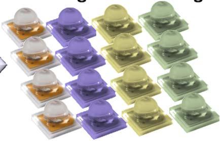
24 High-Power LED Packages Examples Single Large Die (1 die, typical dimension: 0.5 to 1.5 mm) Multiple Large Dice (3 to 25 dice, typical dimension: 0.5 to 1.5 mm each) Small/medium dice Array (20 to 100 dice, typical dimension: 250 to 500 um each) Single or Multi Jumbo Die 1 to 6 dice, typical dimension 2 to 5 mm each) Lumileds Cree Luminus Device Lumileds Luminus Device Osram Osram Cree Osram Edison Opto Luminus Device


 LED die Phosphor Wafer Level Optic")
 Chip to wafer 3)")
 LED package separation.")
25 Wafer Level Packaging (WLP): Packaging of an LED at wafer level, rather than assembling the package of each individual unit after wafer dicing. Packaging wafer LED wafer Note: in this example, the LED chips are singulated before being positioned onto the package wafer (= Chip to Wafer packaging) LED die Phosphor Wafer Level Optic Mirror coating Solder Bump Solder / Metallization 1) Wafer level preparation of the package substrate 2) Chip to wafer 3) Wafer level interconnect, phosphor deposition, encapsulation, optic. 4) LED package separation. Overview of Chip to Wafer LED WLP process Wafer Semicon Level West Packaging 2011


26 Wafer Level Packaging Hymite (technology acquired by Touch Microsystem Technology in 2010) Courtesy of Hymite


27 Wafer Level Packaging Silicon Base Development Inc VisEra Technology Pictures: Company Pictures: Company, System Plus consulting
28 WLP operations for high power LEDs Many LED packaging operations could be carried out at the wafer level: Wafer level Optics 3D Silicon substrates Embedded Zener diodes Wafer level Phosphor coating WLP operations for High Power LEDs Wafer level coating of reflective layer Bumping at the wafer level Wafer to wafer bonding (LED on package substrate)

29 Silicon Substrates and WLP Benefits: Silicon: thermal conductivity, further improved by the use of copper-filled Through Silicon Vias (TSV) Reliability: monolithic assembly, reduced wire interconnect, good CTE match with GaN Wafer level testing Cost: Wafer Level Manufacturing: cost effective. but: Copper-filled TSVs for 3D electrical redistribution and heat dissipation are still expensive. So far only for high performance LEDs Other options: WLP on ceramic substrates. EMC3D TSV Cost of ownership roadmap (courtesy: EVG / EMC3D)


 LED")
30 High Power LED Substrate Market Penetration Forecast by substrate type Yole Développement Note: technology adoption rates for High Power (>1W) LED package only
31 Conclusion: The Path to Cost Reduction Lack of standards: Technology choices application and manufacturer dependent. 10x cost reduction in packaged LEDs cost? Not easy but achievable through a combination of: Technology improvements: efficiency + more lumens per chip. Manufacturing improvements: dedicated LED tools, automation, inline testing. Economies of scale Higher integration Standardization LED industry maturing and reaching critical mass to enable development of dedicated tools. Semiconductor veteran companies bring additional expertise and best practices
Chapter 11 Testing, Assembly, and Packaging
 Chapter 11 Testing, Assembly, and Packaging Professor Paul K. Chu Testing The finished wafer is put on a holder and aligned for testing under a microscope Each chip on the wafer is inspected by a multiple-point
Hermetic Packaging Solutions using Borosilicate Glass Thin Films. Lithoglas Hermetic Packaging Solutions using Borosilicate Glass Thin Films
 Hermetic Packaging Solutions using Borosilicate Glass Thin Films 1 Company Profile Company founded in 2006 ISO 9001:2008 qualified since 2011 Headquarters and Production in Dresden, Germany Production
Diverse Lasers Support Key Microelectronic Packaging Tasks
 Diverse Lasers Support Key Microelectronic Packaging Tasks Written by D Muller, R Patzel, G Oulundsen, H Halou, E Rea 23 July 2018 To support more sophisticated and compact tablets, phones, watches and
Laser Application DAL7020 DFL7020 DFL7161 DFL7160 DFL7341 DFL7360FH DFL7361 DFL7560L. Ablation Process. Stealth Dicing.
 Laser Application Ablation Process Stealth Dicing Laser Lift Off DAL7020 DFL7020 DFL7161 DFL7160 DFL7341 DFL7360FH DFL7361 DFL7560L ABLATION PROCESS DISCO s laser application lineup supports miniaturized
Advanced Packaging Solutions
 Advanced Packaging Solutions by USHIO INC. USHIO s UX Series Providing Advanced Packaging Solutions Page 2 USHIO s UX Series Models Featured @ SEMICON West 2013 Page 2 Large-Size Interposer Stepper UX7-3Di
Lecture: Integration of silicon photonics with electronics. Prepared by Jean-Marc FEDELI CEA-LETI
 Lecture: Integration of silicon photonics with electronics Prepared by Jean-Marc FEDELI CEA-LETI Context The goal is to give optical functionalities to electronics integrated circuit (EIC) The objectives
Advances in Laser Micro-machining for Wafer Probing and Trimming
 Advances in Laser Micro-machining for Wafer Probing and Trimming M.R.H. Knowles, A.I.Bell, G. Rutterford & A. Webb Oxford Lasers June 10, 2002 Oxford Lasers June 2002 1 Introduction to Laser Micro-machining
FLIP CHIP LED SOLDER ASSEMBLY
 As originally published in the SMTA Proceedings FLIP CHIP LED SOLDER ASSEMBLY Gyan Dutt, Srinath Himanshu, Nicholas Herrick, Amit Patel and Ranjit Pandher, Ph.D. Alpha Assembly Solutions South Plainfield,
Yole Developpement. Developpement-v2585/ Publisher Sample
 Yole Developpement http://www.marketresearch.com/yole- Developpement-v2585/ Publisher Sample Phone: 800.298.5699 (US) or +1.240.747.3093 or +1.240.747.3093 (Int'l) Hours: Monday - Thursday: 5:30am - 6:30pm
POSSUM TM Die Design as a Low Cost 3D Packaging Alternative
 POSSUM TM Die Design as a Low Cost 3D Packaging Alternative The trend toward 3D system integration in a small form factor has accelerated even more with the introduction of smartphones and tablets. Integration
CHAPTER 11: Testing, Assembly, and Packaging
 Chapter 11 1 CHAPTER 11: Testing, Assembly, and Packaging The previous chapters focus on the fabrication of devices in silicon or the frontend technology. Hundreds of chips can be built on a single wafer,
Enabling concepts: Packaging Technologies
 Enabling concepts: Packaging Technologies Ana Collado / Liam Murphy ESA / TEC-EDC 01/10/2018 ESA UNCLASSIFIED - For Official Use Enabling concepts: Packaging Technologies Drivers for the future: Higher
Semiconductor Optical Communication Components and Devices Lecture 18: Introduction to Diode Lasers - I
 Semiconductor Optical Communication Components and Devices Lecture 18: Introduction to Diode Lasers - I Prof. Utpal Das Professor, Department of lectrical ngineering, Laser Technology Program, Indian Institute
9 rue Alfred Kastler - BP Nantes Cedex 3 - France Phone : +33 (0) website :
 website :") 9 rue Alfred Kastler - BP 10748-44307 Nantes Cedex 3 - France Phone : +33 (0) 240 180 916 - email : info@systemplus.fr - website : www.systemplus.fr April 2012 - Version 1 Written by: Romain FRAUX DISCLAIMER
9 rue Alfred Kastler - BP 10748-44307 Nantes Cedex 3 - France Phone : +33 (0) 240 180 916 - email : info@systemplus.fr - website : www.systemplus.fr April 2012 - Version 1 Written by: Romain FRAUX DISCLAIMER
Laminate Based Fan-Out Embedded Die Technologies: The Other Option
 Laminate Based Fan-Out Embedded Die Technologies: The Other Option Theodore (Ted) G. Tessier, Tanja Karila*, Tuomas Waris*, Mark Dhaenens and David Clark FlipChip International, LLC 3701 E University Drive
Flexline - A Flexible Manufacturing Method for Wafer Level Packages (Extended Abstract)
") Flexline - A Flexible Manufacturing Method for Wafer Level Packages (Extended Abstract) by Tom Strothmann, *Damien Pricolo, **Seung Wook Yoon, **Yaojian Lin STATS ChipPAC Inc.1711 W Greentree Drive Tempe,
Flexline - A Flexible Manufacturing Method for Wafer Level Packages (Extended Abstract) by Tom Strothmann, *Damien Pricolo, **Seung Wook Yoon, **Yaojian Lin STATS ChipPAC Inc.1711 W Greentree Drive Tempe,
Semiconductor and LED Markets. Jon Sabol Vice President and General Manager Semiconductor and LED Division
 Semiconductor and LED Markets Jon Sabol Vice President and General Manager Semiconductor and LED Division Semiconductor & LED Investing in Semiconductor and LED $ Millions 300 200 27% CAGR 100 0 * FY06
White Light Emitting Diodes. Erick J. Michel Energy Law Spring 2009 Professor Bosselman
 White Light Emitting Diodes Erick J. Michel emichel@kentlaw.edu Energy Law Spring 2009 Professor Bosselman Outline Lighting Energy Use Types of Lighting Some Physics Generating White Light Issues/ Features
TWINSCAN XT:1950i Water-based immersion taken to the max Enabling fast, single-exposure lithography at sub 40 nm
 TWINSCAN XT:1950i Water-based immersion taken to the max Enabling fast, single-exposure lithography at sub 40 nm SEMICON West, San Francisco July 14-18, 2008 Slide 1 The immersion pool becomes an ocean
LEDs A BASIC INTRODUCTION
 LEDs A BASIC INTRODUCTION High Power LEDs Function and construction History Power, flux and luminous efficiency Color and binning LED optics LED: Solid State Lighting Electroluminescence The light is emitted
3D TSV Micro Cu Column Chip-to-Substrate/Chip Assmbly/Packaging Technology
 3D TSV Micro Cu Column Chip-to-Substrate/Chip Assmbly/Packaging Technology by Seung Wook Yoon, *K. T. Kang, W. K. Choi, * H. T. Lee, Andy C. B. Yong and Pandi C. Marimuthu STATS ChipPAC LTD, 5 Yishun Street
New Wave SiP solution for Power
 New Wave SiP solution for Power Vincent Lin Corporate R&D ASE Group APEC March 7 th, 2018 in San Antonio, Texas. 0 Outline Challenges Facing Human Society Energy, Environment and Traffic Autonomous Driving
64 Channel Flip-Chip Mounted Selectively Oxidized GaAs VCSEL Array
 64 Channel Flip-Chip Mounted Selectively Oxidized GaAs VCSEL Array 69 64 Channel Flip-Chip Mounted Selectively Oxidized GaAs VCSEL Array Roland Jäger and Christian Jung We have designed and fabricated
Image Sensor Advanced Package Solution. Prepared by : JL Huang & KingPak RD division
 Image Sensor Advanced Package Solution Prepared by : JL Huang & KingPak RD division Contents CMOS image sensor marketing overview Comparison between different type of CMOS image sensor package Overview
SUPPLEMENTARY INFORMATION
 Room-temperature continuous-wave electrically injected InGaN-based laser directly grown on Si Authors: Yi Sun 1,2, Kun Zhou 1, Qian Sun 1 *, Jianping Liu 1, Meixin Feng 1, Zengcheng Li 1, Yu Zhou 1, Liqun
450mm and Moore s Law Advanced Packaging Challenges and the Impact of 3D
 450mm and Moore s Law Advanced Packaging Challenges and the Impact of 3D Doug Anberg VP, Technical Marketing Ultratech SOKUDO Lithography Breakfast Forum July 10, 2013 Agenda Next Generation Technology
Laser Experts in Semiconductor Manufacturing
 Laser Experts in Semiconductor Manufacturing Backed by more than three decades of experience in laser material processing, ROFIN is one of the best established companies in this field. The company has
Fabricating 2.5D, 3D, 5.5D Devices
 Fabricating 2.5D, 3D, 5.5D Devices Bob Patti, CTO rpatti@tezzaron.com Tezzar on Semiconduct or 04/15/2013 1 Gen4 Dis-Integrated 3D Memory DRAM layers 42nm node 2 million vertical connections per lay per
Silicon Interposers enable high performance capacitors
 Interposers between ICs and package substrates that contain thin film capacitors have been used previously in order to improve circuit performance. However, with the interconnect inductance due to wire
Vertical External Cavity Surface Emitting Laser
 Chapter 4 Optical-pumped Vertical External Cavity Surface Emitting Laser The booming laser techniques named VECSEL combine the flexibility of semiconductor band structure and advantages of solid-state
Silicon Photonics Transceivers for Hyper Scale Datacenters: Deployment and Roadmap
 Silicon Photonics Transceivers for Hyper Scale Datacenters: Deployment and Roadmap Peter De Dobbelaere Luxtera Inc. 09/19/2016 Luxtera Proprietary www.luxtera.com Luxtera Company Introduction $100B+ Shift
ESCC2006 European Supply Chain Convention
 ESCC2006 European Supply Chain Convention PCB Paper 20 Laser Technology for cutting FPC s and PCB s Mark Hüske, Innovation Manager, LPKF Laser & Electronics AG, Germany Laser Technology for cutting FPCs
Basic Guidelines for LED Lamp Package Design
 International Journal of Sustainable and Green Energy 2015; 4(5): 187-194 Published online September 11, 2015 (http://www.sciencepublishinggroup.com/j/ijsge) doi: 10.11648/j.ijrse.20150405.13 Basic Guidelines
Die Prep Considerations for IC Device Applications CORWIL Technology 1635 McCarthy Blvd Milpitas, CA 95035
 Die Prep Considerations for IC Device Applications CORWIL Technology 1635 McCarthy Blvd Milpitas, CA 95035 Jonny Corrao Die Prep While quality, functional parts are the end goal for all semiconductor companies,
The Future of Packaging ~ Advanced System Integration
 The Future of Packaging ~ Advanced System Integration Enabling a Microelectronic World R. Huemoeller SVP, Adv. Product / Platform Develop June 2013 Product Segments End Market % Share Summary 2 New Product
Vixar High Power Array Technology
 Vixar High Power Array Technology I. Introduction VCSELs arrays emitting power ranging from 50mW to 10W have emerged as an important technology for applications within the consumer, industrial, automotive
Through Glass Via (TGV) Technology for RF Applications
 Technology for RF Applications") Through Glass Via (TGV) Technology for RF Applications C. H. Yun 1, S. Kuramochi 2, and A. B. Shorey 3 1 Qualcomm Technologies, Inc. 5775 Morehouse Dr., San Diego, California 92121, USA Ph: +1-858-651-5449,
Through Glass Via (TGV) Technology for RF Applications C. H. Yun 1, S. Kuramochi 2, and A. B. Shorey 3 1 Qualcomm Technologies, Inc. 5775 Morehouse Dr., San Diego, California 92121, USA Ph: +1-858-651-5449,
CMP for More Than Moore
 2009 Levitronix Conference on CMP Gerfried Zwicker Fraunhofer Institute for Silicon Technology ISIT Itzehoe, Germany gerfried.zwicker@isit.fraunhofer.de Contents Moore s Law and More Than Moore Comparison:
Integrated Photonics using the POET Optical InterposerTM Platform
 Integrated Photonics using the POET Optical InterposerTM Platform Dr. Suresh Venkatesan CIOE Conference Shenzhen, China Sept. 5, 2018 POET Technologies Inc. TSXV: PUBLIC POET PTK.V Technologies Inc. PUBLIC
LED technology: MOCVD for SSL. Challenges & Solutions
 SEMICON Europe 2009 Emerging Markets LED technology: MOCVD for SSL Challenges & Solutions Dr. Frank Schulte AIXTRON AG Outline The LED market and its requirements Productivity and cost challenges Solutions
Packaging Roadmap: The impact of miniaturization. Bob Pfahl, inemi Celestica-iNEMI Technology Forum May 15, 2007
 Packaging Roadmap: The impact of miniaturization Bob Pfahl, inemi Celestica-iNEMI Technology Forum May 15, 2007 The Challenges for the Next Decade Addressing the consumer experience using the converged
Innovative Technologies for RF & Power Applications
 Innovative Technologies for RF & Power Applications > Munich > Nov 14, 2017 1 Key Technologies Key Technologies Veeco Market Focus Advanced Packaging, MEMS & RF Lighting, Display & Power Electronics Lithography
Application Note AN-1011
 AN-1011 Board Mounting Application Note for 0.800mm Pitch Devices For part numbers IRF6100, IRF6100PBF, IR130CSP, IR130CSPPBF, IR140CSP, IR140CSPPBF, IR1H40CSP, IR1H40CSPPBF By Hazel Schofield and Philip
Semiconductor Back-Grinding
 Semiconductor Back-Grinding The silicon wafer on which the active elements are created is a thin circular disc, typically 150mm or 200mm in diameter. During diffusion and similar processes, the wafer may
Processes for Flexible Electronic Systems
 Processes for Flexible Electronic Systems Michael Feil Fraunhofer Institut feil@izm-m.fraunhofer.de Outline Introduction Single sheet versus reel-to-reel (R2R) Substrate materials R2R printing processes
Features. Applications. Optional Features
 Features Compact, Rugged Design TEM Beam with M 2 < 1.2 Pulse Rates from Single Shot to 15 khz IR, Green, UV, and Deep UV Wavelengths Available RS232 Computer Control Patented Harmonic Generation Technology
Innovations Push Package-on-Package Into New Markets. Flynn Carson. STATS ChipPAC Inc Kato Rd Fremont, CA 94538
 Innovations Push Package-on-Package Into New Markets by Flynn Carson STATS ChipPAC Inc. 47400 Kato Rd Fremont, CA 94538 Copyright 2010. Reprinted from Semiconductor International, April 2010. By choosing
Innovative Mask Aligner Lithography for MEMS and Packaging
 Innovative Mask Aligner Lithography for MEMS and Packaging Dr. Reinhard Voelkel CEO SUSS MicroOptics SA September 9 th, 2010 1 SUSS Micro-Optics SUSS MicroOptics is a leading supplier for high-quality
Midaz Micro-Slab DPSS Lasers:
 Midaz Micro-Slab DPSS Lasers: Higher power & pulse rate for higher speed micromachining Professor Mike Damzen Midaz Laser Ltd 4 June 2008 AILU Meeting Industrial opportunities in laser micro and nano processing
Semiconductor Lasers Semiconductors were originally pumped by lasers or e-beams First diode types developed in 1962: Create a pn junction in
 Semiconductor Lasers Semiconductors were originally pumped by lasers or e-beams First diode types developed in 1962: Create a pn junction in semiconductor material Pumped now with high current density
Index. Cambridge University Press Silicon Photonics Design Lukas Chrostowski and Michael Hochberg. Index.
 absorption, 69 active tuning, 234 alignment, 394 396 apodization, 164 applications, 7 automated optical probe station, 389 397 avalanche detector, 268 back reflection, 164 band structures, 30 bandwidth
IEEE JOURNAL OF SELECTED TOPICS IN QUANTUM ELECTRONICS 2010 Silicon Photonic Circuits: On-CMOS Integration, Fiber Optical Coupling, and Packaging
 IEEE JOURNAL OF SELECTED TOPICS IN QUANTUM ELECTRONICS 2010 Silicon Photonic Circuits: On-CMOS Integration, Fiber Optical Coupling, and Packaging Christophe Kopp, St ephane Bernab e, Badhise Ben Bakir,
Integrated High Speed VCSELs for Bi-Directional Optical Interconnects
 Integrated High Speed VCSELs for Bi-Directional Optical Interconnects Volodymyr Lysak, Ki Soo Chang, Y ong Tak Lee (GIST, 1, Oryong-dong, Buk-gu, Gwangju 500-712, Korea, T el: +82-62-970-3129, Fax: +82-62-970-3128,
Low Thermal Resistance Flip-Chip Bonding of 850nm 2-D VCSEL Arrays Capable of 10 Gbit/s/ch Operation
 Low Thermal Resistance Flip-Chip Bonding of 85nm -D VCSEL Arrays Capable of 1 Gbit/s/ch Operation Hendrik Roscher In 3, our well established technology of flip-chip mounted -D 85 nm backside-emitting VCSEL
B. Flip-Chip Technology
 B. Flip-Chip Technology B1. Level 1. Introduction to Flip-Chip techniques B1.1 Why flip-chip? In the development of packaging of electronics the aim is to lower cost, increase the packaging density, improve
Trends in Optical Transceivers:
 Trends in Optical Transceivers: Light sources for premises networks Peter Ronco Corning Optical Fiber Asst. Product Line Manager Premises Fibers January 24, 2006 Outline: Introduction: Transceivers and
Innovative ultra-broadband ubiquitous Wireless communications through terahertz transceivers ibrow
 Project Overview Innovative ultra-broadband ubiquitous Wireless communications through terahertz transceivers ibrow Mar-2017 Presentation outline Project key facts Motivation Project objectives Project
Silicon Photonics Technology Platform To Advance The Development Of Optical Interconnects
 Silicon Photonics Technology Platform To Advance The Development Of Optical Interconnects By Mieke Van Bavel, science editor, imec, Belgium; Joris Van Campenhout, imec, Belgium; Wim Bogaerts, imec s associated
IMAPS NE 45 A HETEROGENEOUS SIP SOLUTION FOR RF APPLICATIONS
 IMAPS NE 45 A HETEROGENEOUS SIP SOLUTION FOR RF APPLICATIONS May 1st 2018 Justin C. Borski i3 Microsystems Inc. justin.borski@i3microsystems.com A HETEROGENEOUS SIP SOLUTION FOR RF APPLICATIONS Presentation
Plan Optik AG. Plan Optik AG PRODUCT CATALOGUE
 Plan Optik AG Plan Optik AG PRODUCT CATALOGUE 2 In order to service the high demand of wafers more quickly, Plan Optik provides off the shelf products in sizes from 2 up to 300mm diameter. Therefore Plan
450mm patterning out of darkness Backend Process Exposure Tool SOKUDO Lithography Breakfast Forum July 10, 2013 Doug Shelton Canon USA Inc.
 450mm patterning out of darkness Backend Process Exposure Tool SOKUDO Lithography Breakfast Forum 2013 July 10, 2013 Doug Shelton Canon USA Inc. Introduction Half Pitch [nm] 2013 2014 2015 2016 2017 2018
Flip chip Assembly with Sub-micron 3D Re-alignment via Solder Surface Tension
 Flip chip Assembly with Sub-micron 3D Re-alignment via Solder Surface Tension Jae-Woong Nah*, Yves Martin, Swetha Kamlapurkar, Sebastian Engelmann, Robert L. Bruce, and Tymon Barwicz IBM T. J. Watson Research
Backplane Considerations for an RGB 3D Display Device
 by Daniel Browning, 7.10.14.v.1 0. Introduction This is the third paper in a series that describes a futuristic design for a 3D display device. The first paper introduced the subject and looked at invisibility
Laser MicroJet Technology. Cool Laser Machining.
 Laser MicroJet Technology Cool Laser Machining www.synova.ch Synova S.A., headquartered in Duillier, Switzerland, manufactures leading-edge laser cutting systems since 1997 that incorporate the proprietary
REVISION #25, 12/12/2012
 HYPRES NIOBIUM INTEGRATED CIRCUIT FABRICATION PROCESS #03-10-45 DESIGN RULES REVISION #25, 12/12/2012 Direct all inquiries, questions, comments and suggestions concerning these design rules and/or HYPRES
200mm and 300mm Test Patterned Wafers for Bonding Process Applications SKW ASSOCIATES, INC.
 C M P C h a r a c t e r I z a t I o n S o l u t I o n s 200mm and 300mm Test Patterned Wafers for Bonding Process Applications SKW ASSOCIATES, INC. 2920 Scott Blvd., Santa Clara, CA 95054 Tel: 408-919-0094,
Min Tao, Ph. D, Ashok Prabhu, Akash Agrawal, Ilyas Mohammed, Ph. D, Bel Haba, Ph. D Oct , IWLPC
 PACKAGE-ON-PACKAGE INTERCONNECT FOR FAN-OUT WAFER LEVEL PACKAGES Min Tao, Ph. D, Ashok Prabhu, Akash Agrawal, Ilyas Mohammed, Ph. D, Bel Haba, Ph. D Oct 18-20 2016, IWLPC 1 Outline Laminate to Fan-Out
True Three-Dimensional Interconnections
 True Three-Dimensional Interconnections Satoshi Yamamoto, 1 Hiroyuki Wakioka, 1 Osamu Nukaga, 1 Takanao Suzuki, 2 and Tatsuo Suemasu 1 As one of the next-generation through-hole interconnection (THI) technologies,
Application-Based Opportunities for Reused Fab Lines
 Application-Based Opportunities for Reused Fab Lines Semicon China, March 17 th 2010 Keith Best Simax Lithography S I M A X A L L I A N C E P A R T N E R S Outline Market: Exciting More than Moore applications
SUPPLEMENTARY INFORMATION
 Electrically pumped continuous-wave III V quantum dot lasers on silicon Siming Chen 1 *, Wei Li 2, Jiang Wu 1, Qi Jiang 1, Mingchu Tang 1, Samuel Shutts 3, Stella N. Elliott 3, Angela Sobiesierski 3, Alwyn
A Low-cost Through Via Interconnection for ISM WLP
 A Low-cost Through Via Interconnection for ISM WLP Jingli Yuan, Won-Kyu Jeung, Chang-Hyun Lim, Seung-Wook Park, Young-Do Kweon, Sung Yi To cite this version: Jingli Yuan, Won-Kyu Jeung, Chang-Hyun Lim,
EMERGING SUBSTRATE TECHNOLOGIES FOR PACKAGING
 EMERGING SUBSTRATE TECHNOLOGIES FOR PACKAGING Henry H. Utsunomiya Interconnection Technologies, Inc. Suwa City, Nagano Prefecture, Japan henryutsunomiya@mac.com ABSTRACT This presentation will outline
Envisioning the Future of Optoelectronic Interconnects:
 Envisioning the Future of Optoelectronic Interconnects: The Production Economics of InP and Si Platforms for 100G Ethernet LAN Transceivers Shan Liu Dr. Erica Fuchs Prof. Randolph Kirchain MIT Microphotonics
SOLDER BUMP FLIP CHIP BONDING FOR PIXEL DETECTOR HYBRIDIZATION
 SOLDER BUMP FLIP CHIP BONDING FOR PIXEL DETECTOR HYBRIDIZATION Jorma Salmi and Jaakko Salonen VTT Information Technology Microelectronics P.O. Box 1208 FIN-02044 VTT, Finland (visiting: Micronova, Tietotie
Introduction to Optoelectronic Devices
 Introduction to Optoelectronic Devices Dr. Jing Bai Assistant Professor Department of Electrical and Computer Engineering University of Minnesota Duluth October 30th, 2012 1 Outline What is the optoelectronics?
Generation of a Line Focus for Material Processing from an Array of High Power Diode Laser Bars R. Baettig, N. Lichtenstein, R. Brunner, J.
 Generation of a Line Focus for Material Processing from an Array of High Power Diode Laser Bars R. Baettig, N. Lichtenstein, R. Brunner, J. Müller, B. Valk, M. Kreijci, S. Weiss Overview This slidepack
TSV MEOL (Mid-End-Of-Line) and its Assembly/Packaging Technology for 3D/2.5D Solutions
 and its Assembly/Packaging Technology for 3D/2.5D Solutions") TSV MEOL (Mid-End-Of-Line) and its Assembly/Packaging Technology for 3D/2.5D Solutions Seung Wook YOON, D.J. Na, *K. T. Kang, W. K. Choi, C.B. Yong, *Y.C. Kim and Pandi C. Marimuthu STATS ChipPAC Ltd.
TSV MEOL (Mid-End-Of-Line) and its Assembly/Packaging Technology for 3D/2.5D Solutions Seung Wook YOON, D.J. Na, *K. T. Kang, W. K. Choi, C.B. Yong, *Y.C. Kim and Pandi C. Marimuthu STATS ChipPAC Ltd.
32nm High-K/Metal Gate Version Including 2nd Generation Intel Core processor family
 From Sand to Silicon Making of a Chip Illustrations 32nm High-K/Metal Gate Version Including 2nd Generation Intel Core processor family April 2011 1 The illustrations on the following foils are low resolution
New fabrication and packaging technologies for CMOS pixel sensors: closing gap between hybrid and monolithic
 New fabrication and packaging technologies for CMOS pixel sensors: closing gap between hybrid and monolithic Outline Short history of MAPS development at IPHC Results from TowerJazz CIS test sensor Ultra-thin
(a) All-SiC 2-in-1 module
 All-SiC 2-in-1 module") All-SiC -in- Module CHONABAYASHI, Mikiya * OTOMO, Yoshinori * KARASAWA, Tatsuya * A B S T R A C T Fuji Electric has developed an utilizing a SiC device that has been adopted in the development of a high-performance
All-SiC -in- Module CHONABAYASHI, Mikiya * OTOMO, Yoshinori * KARASAWA, Tatsuya * A B S T R A C T Fuji Electric has developed an utilizing a SiC device that has been adopted in the development of a high-performance
SUSS MA/BA Gen4 Series COMPACT MASK ALIGNER PLATFORM FOR RESEARCH AND LOW-VOLUME PRODUCTION
 SEMI-AUTOMATED MASK ALIGNER SUSS MA/BA Gen4 Series COMPACT MASK ALIGNER PLATFORM FOR RESEARCH AND LOW-VOLUME PRODUCTION SEMI-AUTOMATED MASK ALIGNER SUSS MA/BA Gen4 Series SMART FULL-FIELD EXPOSURE TOOL
Technology for the MEMS processing and testing environment. SUSS MicroTec AG Dr. Hans-Georg Kapitza
 Technology for the MEMS processing and testing environment SUSS MicroTec AG Dr. Hans-Georg Kapitza 1 SUSS MicroTec Industrial Group Founded 1949 as Karl Süss KG GmbH&Co. in Garching/ Munich San Jose Waterbury
Cree TR5050M LEDs CxxxTR5050M-Sxx000
 Cree TR55M LEDs CxxxTR55M-Sxx Data Sheet Cree s TR55M LEDs are the next generation of solid-state LED emitters that combine highly efficient InGaN materials with Cree s proprietary device technology and
Semiconductor Materials for Power Electronics (SEMPEL) GaN power electronics materials
 GaN power electronics materials") Semiconductor Materials for Power Electronics (SEMPEL) GaN power electronics materials Kjeld Pedersen Department of Physics and Nanotechnology, AAU SEMPEL Semiconductor Materials for Power Electronics
Semiconductor Materials for Power Electronics (SEMPEL) GaN power electronics materials Kjeld Pedersen Department of Physics and Nanotechnology, AAU SEMPEL Semiconductor Materials for Power Electronics
UNIVERSITY OF CAMBRIDGE INTERNATIONAL EXAMINATIONS Cambridge International Level 3 Pre-U Certificate Principal Subject
 UNIVERSITY OF CAMBRIDGE INTERNATIONAL EXAMINATIONS Cambridge International Level 3 Pre-U Certificate Principal Subject PHYSICS 9792/02 Paper 2 Part A Written Paper October/November 2013 INSERT The question
Luxeon V Portable. power light source. Technical Data DS40
 power light source TM Luxeon V Portable Technical Data DS4 Luxeon TM is a revolutionary, energy efficient and ultra compact new light source, combining the lifetime and reliability advantages of Light
Chapter 7 Introduction to 3D Integration Technology using TSV
 Chapter 7 Introduction to 3D Integration Technology using TSV Jin-Fu Li Department of Electrical Engineering National Central University Jungli, Taiwan Outline Why 3D Integration An Exemplary TSV Process
Triple i - The key to your success
 Triple i - The key to your success The needs and challenges of today s world are becoming ever more demanding. Standards are constantly rising. Creativity, reliability and high performance are basic prerequisites
IWORID J. Schmitz page 1. Wafer-level CMOS post-processing Jurriaan Schmitz
 IWORID J. Schmitz page 1 Wafer-level CMOS post-processing Jurriaan Schmitz IWORID J. Schmitz page 2 Outline Introduction on wafer-level post-proc. CMOS: a smart, but fragile substrate Post-processing steps
Application Note #15. High Density Pulsed Laser Diode Arrays for SSL Pumping
 Northrop Grumman Cutting Edge Optronics Application Note #15 High Density Pulsed Laser Diode Arrays for SSL Pumping Northrop Grumman Cutting Edge Optronics has developed a new laser diode array package
Application of EOlite Flexible Pulse Technology. Matt Rekow Yun Zhou Nicolas Falletto
 Application of EOlite Flexible Pulse Technology Matt Rekow Yun Zhou Nicolas Falletto 1 Topics Company Background What is a Flexible Pulse Laser? Why Tailored or Flexible Pulse? Application of Flexible
Piezoelectric MEMS: High Performance Oscillators
 Piezoelectric MEMS: High Performance Oscillators March 6 th 2013 Harmeet.Bhugra@idt.com Managing Director MEMS Division, IDT Inc. 2012 Integrated Device Technology, Inc. 1 Introduction to IDT Overview:
SOLDERABLE ANISOTROPIC CONDUCTIVE ADHESIVES FOR 3D PACKAGE APPLICATIONS
 SOLDERABLE ANISOTROPIC CONDUCTIVE ADHESIVES FOR 3D PACKAGE APPLICATIONS ABSTRACT: Dr. Mary Liu and Dr. Wusheng Yin YINCAE Advanced Materials, LLC Albany, NY 3D packaging has recently become very attractive
Lecture 4 INTEGRATED PHOTONICS
 Lecture 4 INTEGRATED PHOTONICS What is photonics? Photonic applications use the photon in the same way that electronic applications use the electron. Devices that run on light have a number of advantages
A new tool for next generation power semiconductors
 A new tool for next generation power semiconductors Cassandra Melvin / SEMICON China / Mach 16, 2018 Technology for tomorrow's solutions Contents 1. HEV/EV market growth 2. Power module packaging 3. EmPower
Strip Detectors. Principal: Silicon strip detector. Ingrid--MariaGregor,SemiconductorsasParticleDetectors. metallization (Al) p +--strips
 p +--strips") Strip Detectors First detector devices using the lithographic capabilities of microelectronics First Silicon detectors -- > strip detectors Can be found in all high energy physics experiments of the last
Strip Detectors First detector devices using the lithographic capabilities of microelectronics First Silicon detectors -- > strip detectors Can be found in all high energy physics experiments of the last
PRESS KIT. High Accuracy Device Bonder with Robotics.
 PRESS KIT High Accuracy Device Bonder with Robotics Press Announcement SET Introduces FC300R High Accuracy Device Bonder with Robotics FC300R: an Easy-to-Use Production Platform Ideal for High Accuracy
CST-90 LEDs. CST-90 Product Datasheet. Features: Table of Contents. Applications
 CST-90 LEDs Features: Extremely high optical output: Over 2,600 lumens from a single chip (White) Table of Contents Technology Overview...2 Test Specifications...2 White Binning Structure...3 Chromaticity
SST-50 W LEDs. SST-50 W Product Datasheet. Features: Table of Contents. Applications
 SST-50 W LEDs Features: Table of Contents Technology Overview...2 Test Specifications...2 White Binning Structure...3 Chromaticity Bins...4 Product Shipping & Labeling Information...7 Electrical Characteristics...8
Applications of Maskless Lithography for the Production of Large Area Substrates Using the SF-100 ELITE. Jay Sasserath, PhD
 Applications of Maskless Lithography for the Production of Large Area Substrates Using the SF-100 ELITE Executive Summary Jay Sasserath, PhD Intelligent Micro Patterning LLC St. Petersburg, Florida Processing