Outline. Introduction on IMEC & IMEC cooperation model. Program Challenges in CMOS scaling
|
|
|
- Alban Powell
- 6 years ago
- Views:
Transcription
1 imec
2 The Role of European Research Institutes in the 450mm Wafer Transition Process IMEC nanoelectronics platform A Collaborative approach towards 450mm R&D IMEC March 2009
3 Outline Introduction on IMEC & IMEC cooperation model Program Challenges in CMOS scaling imec: Today, and path into the future for 450mm European landscape 450mm Conclusions imec
![Resolution, "Shrink" [nm] 200 100 80 60 50 40 30 20 Jan-02 Jan-03 Jan-04 Jan-05 Huge R&D challenge Year of Production Start Jan-06 DRAM Jan-07 Jan-08 Jan-09 Logic Jan-10 Jan-11 Jan-12 NAND Flash](/docs-images/72/66461089/images/4-1.jpg "Jan-13 Jan-14 Relentless reduction of feature size 2D scaling Need for R&D has never been as high Cost of R&D is rapidly increasing Explosion of CAGR New Materials semiconductor industry: 5-7% in")
4 Resolution, "Shrink" [nm] Jan-02 Jan-03 Jan-04 Jan-05 Huge R&D challenge Year of Production Start Jan-06 DRAM Jan-07 Jan-08 Jan-09 Logic Jan-10 Jan-11 Jan-12 NAND Flash Jan-13 Jan-14 Relentless reduction of feature size 2D scaling Need for R&D has never been as high Cost of R&D is rapidly increasing Explosion of CAGR New Materials semiconductor industry: 5-7% in Advanced R&D Devices cost increase per node: 20-30% Outsourcing of R&D to shared R&D platforms Increased use of 3 rd dimension 3D scaling Luc Van den hove imec
5 Partnering for Cost-effective Research Logic IDM Memory IDM Foundries Equipment Suppliers World-wide Build critical mass Centralized Research Share R&D Platform cost Fablite Fabless Regional Government Europe Material Suppliers Luc Van den hove imec
6 IMEC Partner Update 2009Q1 Luc Van den hove imec
7 IMEC Partner Update 2009Q1 Partnerships in core Program IIAP s The World s Largest Industry Commitment to Semiconductor Research in Partnership Lam RESEARCH Luc Van den hove imec
8 IMEC s total revenue (P&L) versus research grant 250 M 2008 revenue: 270 M (est.) 270M Estimated for M Flemish Government Revenue (P&L) imec
9 Outline Introduction on IMEC & IMEC cooperation model Program Challenges in CMOS scaling imec: Today, and path into the future for 450mm European landscape 450mm Conclusions Luc Van den hove imec
10 CMOS scaling Scaling ArF + RET ArF immersion Double Patterning time EUVL Luc Van den hove imec


11 Full field scanner plan ASML XT:1250i NA=0.85 ASML XT:1250 dry NA=0.85 Immersion DPT ASML XT:1700i, NA=1.2 ASML XT:1900i, NA=1.35 Interference printer, NA>1.4 EUVL ASML EUVL α-tool, NA=0.25 ASML EUV Pre-Prod-Tool IMEC intends to continue its leadership in advanced lithography, in immersion as well as EUV, based on an early tool roadmap and proximity collaboration with ASML Luc Van den hove imec

12 EUV lithography Luc Van den hove imec
13 CMOS scaling Ge/IIIV nanowires graphene ArF + RET FinFET metal gate ArF immersion 25 nm HfO 2 high -κ NiSi NiSi FUSI USJ strain Double Patterning silicide time EUVL Luc Van den hove imec
14 CMOS scaling graphene nanowires Ge/IIIV ArF + RET USJ ArF immersion strain NiSi NiSi FUSI 25 nm HfO 2 high -κ metal gate Double Patterning FinFET High-κ, Metal Gate Non-planar devices 16 and beyond High-µ materials, New devices silicide >= Strain, USJ time EUVL Luc Van den hove imec


![E-04 Double Patterning FinFET High-κ, P static [W/stage] Metal Gate RO performance MIPS SMDD (Bulk](/docs-images/72/66461089/images/15-18.jpg "Planar) MIPS psmdd (Bulk Planar) 22-16 Non-planar devices NMOS nmos pmos RO (SMDD) 16 and beyond High-µ")
15 CMOS scaling graphene nanowires 32nm: High-k / metal gate integration Ge/IIIV ArF + RET Gate first Lg=32nm USJ ArF immersion strain Delay/stage [ps] NiSi NiSi 18 FUSI nm HfO 2 high -κ metal gate FET65 (Poly/SiON) FUSI_HiK 8 1.E-10 1.E-09 1.E-08 1.E-07 1.E-06 1.E-05 1.E-04 Double Patterning FinFET High-κ, P static [W/stage] Metal Gate RO performance MIPS SMDD (Bulk Planar) MIPS psmdd (Bulk Planar) Non-planar devices NMOS nmos pmos RO (SMDD) 16 and beyond High-µ materials, New PMOS devices silicide >= Strain, USJ time EUVL Luc Van den hove imec


16 CMOS scaling NiSi poly-si Fin 22nm: FinFET Device graphene 50 nm SOI FF Ge/IIIV nanowires ArF + RET USJ ArF immersion strain NiSi NiSi FUSI 25 nm HfO 2 high -κ metal gate Double Patterning FinFET High-κ, Metal Gate Bulk FF Non-planar devices 16 and beyond High-µ materials, 10 New devices silicide >= Strain, USJ time EUVL Luc Van den hove imec
17 CMOS scaling New materials and devices will be needed to continue the performance scaling Ge/IIIV nanowires graphene ArF + RET USJ ArF immersion strain NiSi NiSi FUSI 25 nm HfO 2 high -κ metal gate Double Patterning FinFET High-κ, Metal Gate Non-planar devices 16 and beyond High-µ materials, New devices silicide >= Strain, USJ time EUVL Luc Van den hove imec
![NVM Roadmap Cell size [F 2 ] Phase Change Memory](/docs-images/72/66461089/images/18-0.jpg "evolutionary disruptive 100 Most mature Embedded memory -")

 RRAM?")

18 NVM Roadmap Cell size [F 2 ] Phase Change Memory evolutionary disruptive 100 Most mature Embedded memory - NOR replacement? FeRAM MRAM niche and embedded applications Spin-based probe memories 10 NOR-Flash (FG/NROM) PCM code 5 TANOS NAND-Flash (FG) RRAM? data x 4x 3x Resistive Switching RAM 2x 1x Technology node F [nm] note: PCM may be applied in embedded applications as well (65nm) OFF R High ON R Low Luc Low Van den hove imec

19 CMOS scaling CNT Air gap 3D TSV graphene 3D SIP Ge/IIIV nanowires Low k k=2.7 Low k k=2.5 metal gate FinFET Low k k= nm HfO 2 high -κ Cu NiSi NiSi FUSI strain USJ silicide time Luc Van den hove imec


20 3D Integration Carrier R&D die Roadmap 3 rd stacked die 3D Interconnect Complexity 3D-SIC 3D-WLP Face-to-Face Flip-Chip Stacked-IC Package 2 nd stacked die 1 st stacked die Landing die Ultra-Thin-Chip Embedding 2-layer UTCS Face-to-Face Micro-bumps 3D-SIP BGA 3D-SIC 2-layer Chip-in-Flex UTCF 3D-WLP 2-layer Through-Si 3D-SIP CSP 3D-SIC N-layer N-layer UTCS 3D-WLP N-layer 3DSIP Die-in-board N-layer UTCS 3D-SIC N-layer UTCS 3D-WLP 3D-SIP A D V A N C E D P A C K A G I N G A N D I N T E R C O N N E C T Research Roadmap 2010 Luc Van den hove imec
21 Global R&D platforms Providing focus for universities and basic insight and solutions for industrial partners Time frame Longer term, many options Shorter term, applications Universities Shared R&D Platforms Industry Lower R&D cost Higher imec
22 Outline Introduction on IMEC & IMEC cooperation model Program Challenges in CMOS scaling imec: Today, and path into the future for 450mm European landscape 450mm Conclusions imec


23 One of the world s most advanced state-of-the-art research facilities Fully operational since July 2006 (~ 500M ) imec
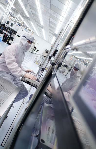
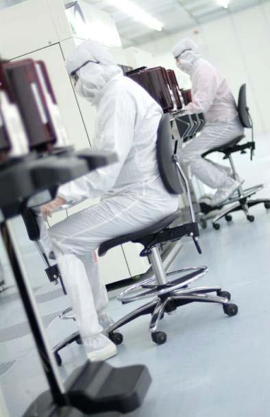
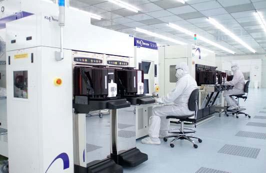
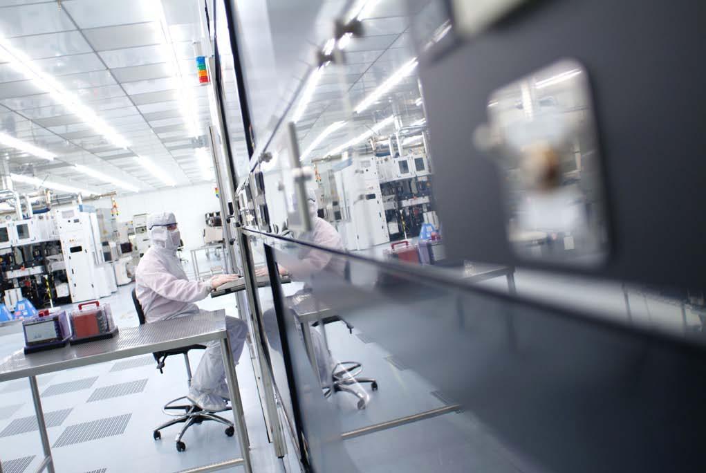
24 Clean Room m 2 Clean Room 300 mm pilot line Ball Room, Clean sub-fab Continuous operation: 24hrs / 7 days IMECAMPUS Clean Room m 2 Clean Room 1750 m 2 Class mm pilot line Continuous operation: 24hrs / 7 days Total: 8000 m 2 Clean Room imec

25 Clean Room m 2 Clean Room 300 mm pilot line Ball Room, Clean sub-fab Continuous operation: 24hrs / 7 days 300mm most advanced scaling R&D IMECAMPUS Total: 8000 m 2 Clean Room imec


26 IMECAMPUS R&D and Prototyping Facility Heterogeneous SOC & SIP Clean Room m 2 Clean Room 1750 m 2 Class mm pilot line Continuous operation: 24hrs / 7 days Total: 8000 m 2 Clean Room imec

27 R&D benefits from gradual transistions example: IIAP processing 200 > 300mm imec
28 An affordable path to 450 mm IMEC s core competence is Process and Device R&D using state-of-the-art processing equipment, including several α- and β-type tools; with world-class operational excellence (cycle time, process quality, process stability, ) with best-in-class fundamental research (materials research, physical characterization, advanced electrical characterziation, ) IMEC plans to continue full integrated process R&D using its 300mm infrastructure during the following years and will therefore further expand its 300mm research infrastructure accordingly IMEC is also expanding its infrastructure to test early 450mm equipment, as soon as requested by its leading partners (preparing for partner pilot lines in 2012) imec
29 FAB m 2 Clean Room 300 mm pilot line Ball Room, Clean sub-fab Continuous operation: 24hrs / 7 days IMECAMPUS Expansion project Clean room Office building (First phase initiated) FAB m 2 Clean Room 1750 m 2 Class mm pilot line Continuous operation: 24hrs / 7 days Total: 8000 m 2 Clean Room imec
30 Concept view Expansion CMORE program Expansion Bio-electronics Lab Expansion Energy (PV) program Expansion 450mm test facility Office Building imec
31 An affordable path to 450 mm IMEC has received approval from the local government for financial support for FAB2 build-out on November 7 th, 2008; Board approval was obtained on November 26 th, 2008: IMEC will start construction in March 2009 (Central Utility Building is available) Timing construction project: Start engineering study: Jan 1, 2008 Start construction: March 2009 End construction: April 2010 imec

32 Construction started on March 17 th, 2009 imec


33 IMEC Clean Room Extension Existing Building Extension clean elevator EUV tool height Plenum 2800 Corridor - Steel Plattform 5800 Lab Cleanroom Make Up Air duct Option: Hoist in the corridor imec
34 An affordable path to 450 mm Planning & decision process Building construction & Facility Preparation Jan 2008 March 2009: Start construction Mid 2010: Construction ready imec
35 An affordable path to 450 mm Engineering Phase 1 Engineering Phase 2 Building construction & Facility Preparation 300 mm process & device research Generic 450 mm modules 450mm Module 1 450mm Module 2 450mm Module 3 imec
36 3-phase program concept for worldwide cooperation towards viable 450mm Assumptions: Economical downturn will affect timeline; timeline will depend on initiative of key IC industry players; R&D should be ready to respond; More than ever, precompetitive R&D is best and most efficient to be done on a central location, shielded from development or production targets 450mm will require new models regarding infrastructure related cooperation; IMEC is interested to take part in this discussion imec
37 3-phase program concept for worldwide cooperation towards viable 450mm mm+ process & device Leuven Leuven-based IMEC network with partners Including build-up of Generic 450 mm modules + + IMEC IMEC Company A? Company B? Program based 300/450 oriented cooperation with industrial partner (or JV, cluster ) and supporting government in locally hosted infrastructure Leuven-based IMEC network with partners 450mm fab with interested partners R&D in new dedicated 450mm infrastructure (EU, TW, JP, US ) 450mm R&D platform requiring new concept - integrated cooperative program Luc Van den hove imec
38 Outline Introduction on IMEC & IMEC cooperation model Program Challenges in CMOS scaling imec: Today, and path into the future for 450mm European landscape 450mm Conclusions imec

39 450mm Views from European R&D
40 Fraunhofer views 42

41 CEA-LETI & 450mm Michel BRILLOUËT CEA Tous droits réservés. Toute reproduction totale ou partielle sur quelque support que ce soit ou utilisation du contenu de ce document est interditesans l autorisation écrite préalable du CEA All rights reserved. Any reproduction in whole or in part on any medium or use of the information contained herein is prohibited without the prior written consent of CEA 450mm, Brussels - Dec. 19, M Brillouët 43

 use for a later development phase when our industrial partners need 450mm")


42 CEA-LETI ready to contribute in 450mm CEA-LETI active in the whole value chain engineered substrates process devices applications which translates 2007 for 450mm in a strong involvement significant contribution (esp. in FEOL & ML2) use for a later development phase when our industrial partners need 450mm independent of wafer diameter CEA Tous droits réservés. Toute reproduction totale ou partielle sur quelque support que ce soit ou utilisation du contenu de ce document est interditesans l autorisation écrite préalable du CEA All rights reserved. Any reproduction in whole or in part on any medium or use of the information contained herein is prohibited without the prior written consent of CEA 450mm, Brussels - Dec. 19, M Brillouët 44


43 with the associated research infrastructure Planned extension for large area substrates 2007 Potential doubling Present mm clean rooms buildings CEA Tous droits réservés. Toute reproduction totale ou partielle sur quelque support que ce soit ou utilisation du contenu de ce document est interditesans l autorisation écrite préalable du CEA All rights reserved. Any reproduction in whole or in part on any medium or use of the information contained herein is prohibited without the prior written consent of CEA 450mm, Brussels - Dec. 19, M Brillouët 45


44 as a part of the project 3,500 6,000 + m² clean rooms 2007 CEA Tous droits réservés. Toute reproduction totale ou partielle sur quelque support que ce soit ou utilisation du contenu de ce document est interditesans l autorisation écrite préalable du CEA All rights reserved. Any reproduction in whole or in part on any medium or use of the information contained herein is prohibited without the prior written consent of CEA 450mm, Brussels - Dec. 19, M Brillouët 46
45 Outline Introduction on IMEC & IMEC cooperation model Program Challenges in CMOS scaling imec: Today, and path into the future for 450mm European landscape 450mm Conclusions imec

46 View from European R&D on 450mm R&D institutes are preparing to be ready will carefully listen and interact with industry for timelines and priority setting R&D institutes discuss cooperation Will share key infrastructure and run complementary programs R&D institutes have role for local industry To help European semiconductor industry in their strategy to be part of worldwide 450mm effort when it happens 2007 R&D institutes will strive for efficiency Via efficient R&D models combining 300mm/450mm 450mm sets for New Cooperation models CEA Tous droits réservés. Toute reproduction totale ou partielle sur quelque support que ce soit ou utilisation du contenu de ce document est interditesans l autorisation écrite préalable du CEA All rights reserved. Any reproduction in whole or in part on any medium or use of the information contained herein is prohibited without the prior written consent of CEA 450mm, Brussels - Dec. 19, M Brillouët 48

47 Concept view 450mm READY imec

48 imec
HOW TO CONTINUE COST SCALING. Hans Lebon
 HOW TO CONTINUE COST SCALING Hans Lebon OUTLINE Scaling & Scaling Challenges Imec Technology Roadmap Wafer size scaling : 450 mm 2 COST SCALING IMPROVED PERFORMANCE 3 GLOBAL TRAFFIC FORECAST Cloud Traffic
PUSHING LITHOGRAPHY TO ENABLE ULTIMATE NANO-ELECTRONICS. LUC VAN DEN HOVE President & CEO imec
 PUSHING LITHOGRAPHY TO ENABLE ULTIMATE NANO-ELECTRONICS LUC VAN DEN HOVE President & CEO imec OUTLINE! Industry drivers! Roadmap extension! Lithography options! Innovation through global collaboration
Competitive in Mainstream Products
 Competitive in Mainstream Products Bert Koek VP, Business Unit manager 300mm Fabs Analyst Day 20 September 2005 ASML Competitive in mainstream products Introduction Market share Device layers critical
IMPACT OF 450MM ON CMP
 IMPACT OF 450MM ON CMP MICHAEL CORBETT MANAGING PARTNER LINX CONSULTING, LLC MCORBETT@LINX-CONSULTING.COM PREPARED FOR CMPUG JULY 2011 LINX CONSULTING Outline 1. Overview of Linx Consulting 2. CMP Outlook/Drivers
IMEC's Collaboration Models for Nanoelectronics Research and Role of the PRINS Research Infrastructure
 IMEC's Collaboration Models for Nanoelectronics Research and Role of the PRINS Research Infrastructure * IMEC, Kapeldreef 75, 3001 Leuven, Belgium *Also E.E. Dept, KU Leuven, Kasteelpark Arenberg 10, 3001
450mm and Moore s Law Advanced Packaging Challenges and the Impact of 3D
 450mm and Moore s Law Advanced Packaging Challenges and the Impact of 3D Doug Anberg VP, Technical Marketing Ultratech SOKUDO Lithography Breakfast Forum July 10, 2013 Agenda Next Generation Technology
TWINSCAN XT:1950i Water-based immersion taken to the max Enabling fast, single-exposure lithography at sub 40 nm
 TWINSCAN XT:1950i Water-based immersion taken to the max Enabling fast, single-exposure lithography at sub 40 nm SEMICON West, San Francisco July 14-18, 2008 Slide 1 The immersion pool becomes an ocean
NANOELECTRONIC TECHNOLOGY: CHALLENGES IN THE 21st CENTURY
 NANOELECTRONIC TECHNOLOGY: CHALLENGES IN THE 21st CENTURY S. M. SZE National Chiao Tung University Hsinchu, Taiwan And Stanford University Stanford, California ELECTRONIC AND SEMICONDUCTOR INDUSTRIES
Lithography Industry Collaborations
 Accelerating the next technology revolution Lithography Industry Collaborations SOKUDO Breakfast July 13, 2011 Stefan Wurm SEMATECH Copyright 2009 SEMATECH, Inc. SEMATECH, and the SEMATECH logo are registered
EUV Supporting Moore s Law
 EUV Supporting Moore s Law Marcel Kemp Director Investor Relations - Europe DB 2014 TMT Conference London September 4, 2014 Forward looking statements This document contains statements relating to certain
Beyond Moore the challenge for Europe
 Beyond Moore the challenge for Europe Dr. Alfred J. van Roosmalen Vice-President Business Development, NXP Semiconductors Company member of MEDEA+/CATRENE/AENEAS/Point-One FIT-IT 08 Spring Research Wien,
Fin-Shaped Field Effect Transistor (FinFET) Min Ku Kim 03/07/2018
 Min Ku Kim 03/07/2018") Fin-Shaped Field Effect Transistor (FinFET) Min Ku Kim 03/07/2018 ECE 658 Sp 2018 Semiconductor Materials and Device Characterizations OUTLINE Background FinFET Future Roadmap Keeping up w/ Moore s Law
Fin-Shaped Field Effect Transistor (FinFET) Min Ku Kim 03/07/2018 ECE 658 Sp 2018 Semiconductor Materials and Device Characterizations OUTLINE Background FinFET Future Roadmap Keeping up w/ Moore s Law
Technology & Manufacturing
 Technology & Manufacturing Jean-Marc Chery Chief Operating Officer Front-End Manufacturing Unique capability 2 Technology portfolio aligned with application focus areas Flexible IDM model with foundry
45nm Foundry CMOS with Mask-Lite Reduced Mask Costs
 This work is sponsored in part by the Air Force Research Laboratory (AFRL/RVSE) 45nm Foundry CMOS with Mask-Lite Reduced Mask Costs 21 March 2012 This work is sponsored in part by the National Aeronautics
IC Knowledge LLC, PO Box 20, Georgetown, MA Ph: (978) , Fx: (978)
 , Fx: (978)") IC Knowledge LLC, PO Box 20, Georgetown, MA 01833 www.icknowledge.com Ph: (978) 352 7610, Fx: (978) 352 3870 Linx Consulting, PO Box 384, Mendon, MA 01756 0384 www.linxconsulting.com Ph: (617) 273 8837
IC Knowledge LLC, PO Box 20, Georgetown, MA 01833 www.icknowledge.com Ph: (978) 352 7610, Fx: (978) 352 3870 Linx Consulting, PO Box 384, Mendon, MA 01756 0384 www.linxconsulting.com Ph: (617) 273 8837
Chapter 15 Summary and Future Trends
 Chapter 15 Summary and Future Trends Hong Xiao, Ph. D. hxiao89@hotmail.com www2.austin.cc.tx.us/hongxiao/book.htm Hong Xiao, Ph. D. www2.austin.cc.tx.us/hongxiao/book.htm 1 The 1960s First IC product Bipolar
Enabling Breakthroughs In Technology
 Enabling Breakthroughs In Technology Mike Mayberry Director of Components Research VP, Technology and Manufacturing Group Intel Corporation June 2011 Defined To be defined Enabling a Steady Technology
The SEMATECH Model: Potential Applications to PV
 Continually cited as the model for a successful industry/government consortium Accelerating the next technology revolution The SEMATECH Model: Potential Applications to PV Dr. Michael R. Polcari President
Extending The Life Of 200mm Fabs And The Re-use of Second Hand Tools
 Extending The Life Of 200mm Fabs And The Re-use of Second Hand Tools Gareth Bignell, FE Equipment Procurement Director SEMICON Europa 2012 Presentation Summary 2 An introduction to STMicroelectronics The
Holistic View of Lithography for Double Patterning. Skip Miller ASML
 Holistic View of Lithography for Double Patterning Skip Miller ASML Outline Lithography Requirements ASML Holistic Lithography Solutions Conclusions Slide 2 Shrink Continues Lithography keeps adding value
Lithography Roadmap. without immersion lithography. Node Half pitch. 248nm. 193nm. 157nm EUVL. 3-year cycle: 2-year cycle: imec 2005
 Lithography Roadmap without immersion lithography Node Half pitch 180 nm 130 nm 90 nm 65 nm 45 nm 32 nm 22 nm 250 nm 180 nm 130 nm 90 nm 65 nm 45 nm 32 nm 248nm 193nm 157nm EUVL 3-year cycle: 2-year cycle:
EMERGING SUBSTRATE TECHNOLOGIES FOR PACKAGING
 EMERGING SUBSTRATE TECHNOLOGIES FOR PACKAGING Henry H. Utsunomiya Interconnection Technologies, Inc. Suwa City, Nagano Prefecture, Japan henryutsunomiya@mac.com ABSTRACT This presentation will outline
Innovation to Advance Moore s Law Requires Core Technology Revolution
 Innovation to Advance Moore s Law Requires Core Technology Revolution Klaus Schuegraf, Ph.D. Chief Technology Officer Silicon Systems Group Applied Materials UC Berkeley Seminar March 9 th, 2012 Innovation
Advanced PDK and Technologies accessible through ASCENT
 Advanced PDK and Technologies accessible through ASCENT MOS-AK Dresden, Sept. 3, 2018 L. Perniola*, O. Rozeau*, O. Faynot*, T. Poiroux*, P. Roseingrave^ olivier.faynot@cea.fr *Cea-Leti, Grenoble France;
Thermal Management in the 3D-SiP World of the Future
 Thermal Management in the 3D-SiP World of the Future Presented by W. R. Bottoms March 181 th, 2013 Smaller, More Powerful Portable Devices Are Driving Up Power Density Power (both power delivery and power
The Development of the Semiconductor CVD and ALD Requirement
 The Development of the Semiconductor CVD and ALD Requirement 1 Linx Consulting 1. We create knowledge and develop unique insights at the intersection of electronic thin film processes and the chemicals
EUROSOI+- FP of 38 30/06/ FINAL PUBLISHABLE SUMMARY REPORT
 EUROSOI+- FP7-216373 3 of 38 30/06/2011 1. FINAL PUBLISHABLE SUMMARY REPORT EUROSOI+- FP7-216373 4 of 38 30/06/2011 EUROSOI+- FP7-216373 5 of 38 30/06/2011 The main and last objective of EUROSOI Network
Chapter 7 Introduction to 3D Integration Technology using TSV
 Chapter 7 Introduction to 3D Integration Technology using TSV Jin-Fu Li Department of Electrical Engineering National Central University Jungli, Taiwan Outline Why 3D Integration An Exemplary TSV Process
The Future of Packaging ~ Advanced System Integration
 The Future of Packaging ~ Advanced System Integration Enabling a Microelectronic World R. Huemoeller SVP, Adv. Product / Platform Develop June 2013 Product Segments End Market % Share Summary 2 New Product
Lithography in our Connected World
 Lithography in our Connected World SEMI Austin Spring Forum TOP PAN P R INTING CO., LTD MATER IAL SOLUTIONS DIVISION Toppan Printing Co., LTD A Broad-Based Global Printing Company Foundation: January 17,
ITRS MOSFET Scaling Trends, Challenges, and Key Technology Innovations
 Workshop on Frontiers of Extreme Computing Santa Cruz, CA October 24, 2005 ITRS MOSFET Scaling Trends, Challenges, and Key Technology Innovations Peter M. Zeitzoff Outline Introduction MOSFET scaling and
MAPPER: High throughput Maskless Lithography
 MAPPER: High throughput Maskless Lithography Marco Wieland CEA- Leti Alterative Lithography workshop 1 Today s agenda Introduction Applications Qualification of on-tool metrology by in-resist metrology
Used Semiconductor Manufacturing Equipment: Looking for Sales in All the Right Places. Study Number MA108-09
 Study Number MA108-09 August 2009 Copyright Semico Research, 2009. All rights reserved. Reproduction in whole or part is prohibited without permission of Semico. The contents of this report represent
POSSUM TM Die Design as a Low Cost 3D Packaging Alternative
 POSSUM TM Die Design as a Low Cost 3D Packaging Alternative The trend toward 3D system integration in a small form factor has accelerated even more with the introduction of smartphones and tablets. Integration
Technology Transfers Opportunities, Process and Risk Mitigation. Radhika Srinivasan, Ph.D. IBM
 Technology Transfers Opportunities, Process and Risk Mitigation Radhika Srinivasan, Ph.D. IBM Abstract Technology Transfer is quintessential to any technology installation or semiconductor fab bring up.
IMI Labs Semiconductor Applications. June 20, 2016
 IMI Labs Semiconductor Applications June 20, 2016 Materials Are At the Core of Innovation in the 21st Century Weight Space Flexibility Heat Management Lightweight Energy Efficient Temperature Energy Efficient
Newer process technology (since 1999) includes :
 includes :") Newer process technology (since 1999) includes : copper metalization hi-k dielectrics for gate insulators si on insulator strained silicon lo-k dielectrics for interconnects Immersion lithography for masks
Newer process technology (since 1999) includes : copper metalization hi-k dielectrics for gate insulators si on insulator strained silicon lo-k dielectrics for interconnects Immersion lithography for masks
NEXT GENERATION SILICON PHOTONICS FOR COMPUTING AND COMMUNICATION PHILIPPE ABSIL
 NEXT GENERATION SILICON PHOTONICS FOR COMPUTING AND COMMUNICATION PHILIPPE ABSIL OUTLINE Introduction Platform Overview Device Library Overview What s Next? Conclusion OUTLINE Introduction Platform Overview
Integration of 3D detector systems
 Integration of 3D detector systems Piet De Moor Introduction Evolution in radiation detection/imaging: single pixel linear array 2D array increase in resolution = decrease in pitch (down to few um) = thanks
Intel Technology Journal
 Volume 06 Issue 02 Published, May 16, 2002 ISSN 1535766X Intel Technology Journal Semiconductor Technology and Manufacturing The Intel Lithography Roadmap A compiled version of all papers from this issue
research in the fields of nanoelectronics
 FRAUNHOFEr center Nanoelectronic Technologies research in the fields of nanoelectronics 1 contents Fraunhofer CNT in Profile 3 Competence Areas Analytics 4 Functional Electronic Materials 5 Device & Integration
Intel's 65 nm Logic Technology Demonstrated on 0.57 µm 2 SRAM Cells
 Intel's 65 nm Logic Technology Demonstrated on 0.57 µm 2 SRAM Cells Mark Bohr Intel Senior Fellow Director of Process Architecture & Integration Intel 1 What are We Announcing? Intel has fabricated fully-functional
45nm Foundry CMOS with Mask-Lite Reduced Mask Costs
 This work is sponsored by the Air Force Research Laboratory (AFRL/RVSE) TPOC: Mr. Kenneth Hebert 45nm Foundry CMOS with Mask-Lite Reduced Mask Costs 25 October 2011 www.americansemi.com 2011 American Semiconductor,
Fraunhofer IZM - ASSID
 FRAUNHOFER-INSTITUT FÜR Zuverlässigkeit und Mikrointegration IZM Fraunhofer IZM - ASSID All Silicon System Integration Dresden Heterogeneous 3D Wafer Level System Integration 3D system integration is one
IMEC update. A.M. Goethals. IMEC, Leuven, Belgium
 IMEC update A.M. Goethals IMEC, Leuven, Belgium Outline IMEC litho program overview ASML ADT status 1 st imaging Tool description Resist projects Screening using interference litho K LUP / Novel resist
Transistor Scaling in the Innovation Era. Mark Bohr Intel Senior Fellow Logic Technology Development August 15, 2011
 Transistor Scaling in the Innovation Era Mark Bohr Intel Senior Fellow Logic Technology Development August 15, 2011 MOSFET Scaling Device or Circuit Parameter Scaling Factor Device dimension tox, L, W
ICT Micro- and nanoelectronics technologies
 EPoSS Proposers' Day, 2 Feb 2017, Brussels ICT 31-2017 Micro- and nanoelectronics technologies Eric Fribourg-Blanc, Henri Rajbenbach, Andreas Lymberis European Commission DG CONNECT (Communications Networks,
Status and Perspectives of the European Semiconductor Industry. Andreas Wild
 Status and Perspectives of the European Semiconductor Industry Andreas Wild Content 1. 2011 for the European Semiconductors Industry 2. Public-Private Partnership 3. Key Enabling Technologies: Pilot Lines
EUV lithography: today and tomorrow
 EUV lithography: today and tomorrow Vadim Banine, Stuart Young, Roel Moors Dublin, October 2012 Resolution/half pitch, "Shrink" [nm] EUV DPT ArFi ArF KrF Industry roadmap towards < 10 nm resolution Lithography
DUV. Matthew McLaren Vice President Program Management, DUV. 24 November 2014
 DUV Matthew McLaren Vice President Program Management, DUV 24 Forward looking statements This document contains statements relating to certain projections and business trends that are forward-looking,
3D Integration developments & manufacturing CEA-LETI. D. Henry CEA-Leti-Minatec
 3D Integration developments & manufacturing offer @ CEA-LETI D. Henry CEA-Leti-Minatec Outline Introduction 3D Integration R&D activities overview 3D integration Manufacturing offer : Open 3D platform
Advanced Digital Integrated Circuits. Lecture 2: Scaling Trends. Announcements. No office hour next Monday. Extra office hour Tuesday 2-3pm
 EE241 - Spring 20 Advanced Digital Integrated Circuits Lecture 2: Scaling Trends and Features of Modern Technologies Announcements No office hour next Monday Extra office hour Tuesday 2-3pm 2 1 Outline
Organic Packaging Substrate Workshop Overview
 Organic Packaging Substrate Workshop Overview Organized by: International Electronics Manufacturing Initiative (inemi) Mario A. Bolanos November 17-18, 2009 1 Organic Packaging Substrate Workshop Work
TechSearch International, Inc. Corporate Overview E. Jan Vardaman, President
 TechSearch International, Inc. Corporate Overview E. Jan Vardaman, President Corporate Background Founded in 1987 and headquartered in Austin, Texas Recognized around the world as a leading consulting
«Single European Semiconductor Strategy: Industry s Vision for Europe»
 «Single European Semiconductor Strategy: Industry s Vision for Europe» Alain Astier STMicroelectronics Silicon Technology & Manufacturing Group Vice-President Strategic Programs SEMI BRUSSELS FORUM, MAY
Recent Developments in Multifunctional Integration. Stephan Guttowski, Head of Technology Park»Heterointegration«, Fraunhofer FMD
 Recent Developments in Multifunctional Integration Stephan Guttowski, Head of Technology Park»Heterointegration«, Fraunhofer FMD Founding Participants 2 One-Stop-Shop for developments from wafer technologies
Multiple Patterning for Immersion Extension and EUV Insertion. Chris Bencher Distinguished Member of Technical Staff Applied Materials CTO group
 Multiple Patterning for Immersion Extension and EUV Insertion Chris Bencher Distinguished Member of Technical Staff Applied Materials CTO group Abstract Multiple Patterning for Immersion Extension and
Collaboration: The Semiconductor Industry s Path to Survival and Growth
 Collaboration: The Semiconductor Industry s Path to Survival and Growth Dr. Michael R. Polcari President and CEO SEMATECH 15 March 2005 3/17/2005 J:\ADMCTR\OCE\M_Polcari\ITPC 10-04 1 Outline Environment
ISSCC 2003 / SESSION 1 / PLENARY / 1.1
 ISSCC 2003 / SESSION 1 / PLENARY / 1.1 1.1 No Exponential is Forever: But Forever Can Be Delayed! Gordon E. Moore Intel Corporation Over the last fifty years, the solid-state-circuits industry has grown
Progress in full field EUV lithography program at IMEC
 Progress in full field EUV lithography program at IMEC A.M. Goethals*, G.F. Lorusso*, R. Jonckheere*, B. Baudemprez*, J. Hermans*, F. Iwamoto 1, B.S. Kim 2, I.S. Kim 2, A. Myers 3, A. Niroomand 4, N. Stepanenko
EUVL getting ready for volume introduction
 EUVL getting ready for volume introduction SEMICON West 2010 Hans Meiling, July 14, 2010 Slide 1 public Outline ASML s Lithography roadmap to support Moore s Law Progress on 0.25NA EUV systems Progress
Fabricating 2.5D, 3D, 5.5D Devices
 Fabricating 2.5D, 3D, 5.5D Devices Bob Patti, CTO rpatti@tezzaron.com Tezzar on Semiconduct or 04/15/2013 1 Gen4 Dis-Integrated 3D Memory DRAM layers 42nm node 2 million vertical connections per lay per
Bank of America Merrill Lynch Taiwan, Technology and Beyond Conference
 Bank of America Merrill Lynch Taiwan, Technology and Beyond Conference Craig De Young Vice President Investor Relations Taipei, Taiwan March 12, 2013 Forward looking statements Slide 2 Safe Harbor Statement
Low-Power VLSI. Seong-Ook Jung VLSI SYSTEM LAB, YONSEI University School of Electrical & Electronic Engineering
 Low-Power VLSI Seong-Ook Jung 2013. 5. 27. sjung@yonsei.ac.kr VLSI SYSTEM LAB, YONSEI University School of Electrical & Electronic Engineering Contents 1. Introduction 2. Power classification & Power performance
ECE 5745 Complex Digital ASIC Design Topic 2: CMOS Devices
 ECE 5745 Complex Digital ASIC Design Topic 2: CMOS Devices Christopher Batten School of Electrical and Computer Engineering Cornell University http://www.csl.cornell.edu/courses/ece5950 Simple Transistor
Noel Technologies. Provider of Advanced Lithography and Semiconductor Thin Film Services
 Noel Technologies Provider of Advanced Lithography and Semiconductor Thin Film Services Noel Technologies Keith Best Biography Over the last 27 years, Keith Best has held a variety of semiconductor processing
Sustaining the Si Revolution: From 3D Transistors to 3D Integration
 Sustaining the Si Revolution: From 3D Transistors to 3D Integration Tsu Jae King Liu Department of Electrical Engineering and Computer Sciences University of California, Berkeley, CA USA February 23, 2015
High-Performance Si Nanowire FET with a Semi Gate-Around Structure Suitable for Integration
 High-Performance Si Nanowire FET with a Semi Gate-Around Structure Suitable for Integration Soshi Sato 1, Hideyuki Kamimura 1, Hideaki Arai 1, Kuniyuki Kakushima 2, Parhat Ahmet 1, Kenji Ohmori 3, Keisaku
BCD Smart Power Roadmap Trends and Challenges. Giuseppe Croce NEREID WORKSHOP Smart Energy Bertinoro, October 20 th
 BCD Smart Power Roadmap Trends and Challenges Giuseppe Croce NEREID WORKSHOP Smart Energy Bertinoro, October 20 th Outline 2 Introduction Major Trends in Smart Power ASICs An insight on (some) differentiating
New Process Technologies Will silicon CMOS carry us to the end of the Roadmap?
 HPEC Workshop 2006 New Process Technologies Will silicon CMOS carry us to the end of the Roadmap? Craig L. Keast, Chenson Chen, Mike Fritze, Jakub Kedzierski, Dave Shaver HPEC 2006-1 Outline A brief history
The future of lithography and its impact on design
 The future of lithography and its impact on design Chris Mack www.lithoguru.com 1 Outline History Lessons Moore s Law Dennard Scaling Cost Trends Is Moore s Law Over? Litho scaling? The Design Gap The
Limitations and Challenges to Meet Moore's Law
 Limitations and Challenges to Meet Moore's Law Sept 10, 2015 Sung Kim sung_kim@amat.com State of the art: cleanroom toolsets metrology analysis module development test & reliability Introduction Why do
Packaging Roadmap: The impact of miniaturization. Bob Pfahl, inemi Celestica-iNEMI Technology Forum May 15, 2007
 Packaging Roadmap: The impact of miniaturization Bob Pfahl, inemi Celestica-iNEMI Technology Forum May 15, 2007 The Challenges for the Next Decade Addressing the consumer experience using the converged
SAMPLE SLIDES & COURSE OUTLINE. Core Competency In Semiconductor Technology: 2. FABRICATION. Dr. Theodore (Ted) Dellin
 Dellin") & Digging Deeper Devices, Fabrication & Reliability For More Info:.com or email Dellin@ieee.org SAMPLE SLIDES & COURSE OUTLINE In : 2. A Easy, Effective, of How Devices Are.. Recommended for everyone who
& Digging Deeper Devices, Fabrication & Reliability For More Info:.com or email Dellin@ieee.org SAMPLE SLIDES & COURSE OUTLINE In : 2. A Easy, Effective, of How Devices Are.. Recommended for everyone who
Beyond Immersion Patterning Enablers for the Next Decade
 Beyond Immersion Patterning Enablers for the Next Decade Colin Brodsky Manager and Senior Technical Staff Member Patterning Process Development IBM Semiconductor Research & Development Center Hopewell
Programmi di ricerca del VII Framework
 Programmi di ricerca del VII Framework 24 Novembre 2007 Research Lines Ultimate CMOS Beyond CMOS Non-volatile Memories Ultimate F/G and Emerging - 2 - More Moore Beyond CMOS - 3 - Flash cell evolution
Scaling of Semiconductor Integrated Circuits and EUV Lithography
 Scaling of Semiconductor Integrated Circuits and EUV Lithography ( 半導体集積回路の微細化と EUV リソグラフィー ) December 13, 2016 EIDEC (Emerging nano process Infrastructure Development Center, Inc.) Hidemi Ishiuchi 1 OUTLINE
A New Era in Nanotechnology Research: The Industry-University-Government Cooperative Model
 A New Era in Nanotechnology Research: The Industry-University-Government Cooperative Model May 18, 2010 AVP Business Development, Alliances and Consortia Professor of Nanoengineering IBM Distinguished
Plan Optik AG. Plan Optik AG PRODUCT CATALOGUE
 Plan Optik AG Plan Optik AG PRODUCT CATALOGUE 2 In order to service the high demand of wafers more quickly, Plan Optik provides off the shelf products in sizes from 2 up to 300mm diameter. Therefore Plan
EUVL Scanners Operational at Chipmakers. Skip Miller Semicon West 2011
 EUVL Scanners Operational at Chipmakers Skip Miller Semicon West 2011 Outline ASML s Lithography roadmap to support Moore s Law Progress on NXE:3100 (0.25NA) EUV systems Progress on NXE:3300 (0.33NA) EUV
Disruptive Developments for Advanced Die Attach to Tackle the Challenges of Heterogeneous Integration
 Disruptive Developments for Advanced Die Attach to Tackle the Challenges of Heterogeneous Integration Hugo Pristauz & Andreas Mayr, Besi Austria presented by: Stefan Behler, Besi Switzerland ECTC 2018
Process Variability and the SUPERAID7 Approach
 Process Variability and the SUPERAID7 Approach Jürgen Lorenz Fraunhofer Institut für Integrierte Systeme und Bauelementetechnologie IISB, Erlangen, Germany ESSDERC/ ESSCIRC Workshop Process Variations
Device architectures for the 5nm technology node and beyond Nadine Collaert
 Device architectures for the 5nm technology node and beyond Nadine Collaert Distinguished member of technical staff, imec Outline Introduction Beyond FinFET: lateral nanowires and vertical transistors
Lecture: Integration of silicon photonics with electronics. Prepared by Jean-Marc FEDELI CEA-LETI
 Lecture: Integration of silicon photonics with electronics Prepared by Jean-Marc FEDELI CEA-LETI Context The goal is to give optical functionalities to electronics integrated circuit (EIC) The objectives
Market and technology trends in advanced packaging
 Close Market and technology trends in advanced packaging Executive OVERVIEW Recent advances in device miniaturization trends have placed stringent requirements for all aspects of product manufacturing.
Innovations Push Package-on-Package Into New Markets. Flynn Carson. STATS ChipPAC Inc Kato Rd Fremont, CA 94538
 Innovations Push Package-on-Package Into New Markets by Flynn Carson STATS ChipPAC Inc. 47400 Kato Rd Fremont, CA 94538 Copyright 2010. Reprinted from Semiconductor International, April 2010. By choosing
Trends in Advanced Packaging Technologies An IMAPS UK view
 Trends in Advanced Packaging Technologies An IMAPS UK view Andy Longford Chair IMAPS UK 2007 9 PandA Europe IMAPS UK IeMRC Interconnection event December 2008 1 International Microelectronics And Packaging
Value Creation of AI in the Manufacturing Industry
 Value Creation of AI in the Manufacturing Industry Janet George Fellow/Chief Data Scientist Western Digital Corporation September 28 th, 2016 2016 Western Digital Corporation or its affiliates. All rights
Status and challenges of EUV Lithography
 Status and challenges of EUV Lithography SEMICON Europa Dresden, Germany Jan-Willem van der Horst Product Manager EUV October 10 th, 2013 Slide 2 Contents Introduction NXE:3100 NXE:3300B Summary and acknowledgements
Opportunities and Challenges for Nanoelectronic Devices and Processes
 The Sixth U.S.-Korea Forum on Nanotechnology, April 28-29, 2009, Las Vegas, NV Opportunities and Challenges for Nanoelectronic Devices and Processes Yoshio Nishi Professor, Electrical Engineering, Material
Legacy & Leading Edge Both are Winners
 Legacy & Leading Edge Both are Winners Semicon CMP User Group July 16, 2015 Sue Davis 408-833-5905 CMP Team Contributors: Mike Fury, Ph.D. Karey Holland, Ph.D. Jerry Yang, Ph.D. www.techcet.com 1 Outline
Manufacturing Case Studies: Copy Exactly (CE!) and the two-year cycle at Intel
 and the two-year cycle at Intel") Manufacturing Case Studies: Copy Exactly (CE!) and the two-year cycle at Intel Paolo A. Gargini Director Technology Strategy Intel Fellow 1 Agenda 2-year cycle Copy Exactly Conclusions 2 I see no reason
Manufacturing Case Studies: Copy Exactly (CE!) and the two-year cycle at Intel Paolo A. Gargini Director Technology Strategy Intel Fellow 1 Agenda 2-year cycle Copy Exactly Conclusions 2 I see no reason
Introduction to CMC 3D Test Chip Project
 Introduction to CMC 3D Test Chip Project Robert Mallard CMC Microsystems Apr 20, 2011 1 Overview of today s presentation Introduction to the project objectives CMC Why 3D chip stacking? The key to More
EMT 251 Introduction to IC Design
 EMT 251 Introduction to IC Design (Pengantar Rekabentuk Litar Terkamir) Semester II 2011/2012 Introduction to IC design and Transistor Fundamental Some Keywords! Very-large-scale-integration (VLSI) is
IDeAL program : DSA activity at LETI. S. Tedesco R. Tiron L. Pain
 IDeAL program : DSA activity at LETI S. Tedesco R. Tiron L. Pain Outline Why DSA for microelectronics The IDeAL progam Graphoepitaxy of BCP Contact hole application 300 mm pilot line in LETI Conclusion
EUV lithography: status, future requirements and challenges
 EUV lithography: status, future requirements and challenges EUVL Dublin Vadim Banine with the help of Rudy Peters, David Brandt, Igor Fomenkov, Maarten van Kampen, Andrei Yakunin, Vladimir Ivanov and many
A Perspective on Semiconductor Equipment. R. B. Herring March 4, 2004
 A Perspective on Semiconductor Equipment R. B. Herring March 4, 2004 Outline Semiconductor Industry Overview of circuit fabrication Semiconductor Equipment Industry Some equipment business strategies Product
Credit Suisse European Technology Conference 2008
 Credit Suisse European Technoogy Conference 2008 ASML continues to execute its eadership strategy and expects gradua order pick-up Franki D Hoore Director European Investor Reations London, 15 May 2008
Yole Developpement. Developpement-v2585/ Publisher Sample
 Yole Developpement http://www.marketresearch.com/yole- Developpement-v2585/ Publisher Sample Phone: 800.298.5699 (US) or +1.240.747.3093 or +1.240.747.3093 (Int'l) Hours: Monday - Thursday: 5:30am - 6:30pm
G450C. Global 450mm Consortium at CNSE. Michael Liehr, General Manager G450C, Vice President for Research
 Global 450mm Consortium at CNSE Michael Liehr, General Manager G450C, Vice President for Research - CNSE Overview - G450C Vision - G450C Mission - Org Structure - Scope - Timeline The Road Ahead for Nano-Fabrication