Wide Band-Gap Power Device
|
|
|
- Abigail Jenkins
- 5 years ago
- Views:
Transcription
1 Wide Band-Gap Power Device 1 Contents Revisit silicon power MOSFETs Silicon limitation Silicon solution Wide Band-Gap material Characteristic of SiC Power Device Characteristic of GaN Power Device 2 1
2 Power semiconductor Voltage Range 3 MOSFET 4 2
 is independent of drain current, but depends on gate voltage and so")
3 DMOS in the forward blocking state 5 On-state Losses In the On-state the resistance R DS(ON) is a key figure of merit (FOM) for a MOSFET The value naturally depends on the voltage rating of a device since the epi-layer will have a higher resistance for higher voltage devices For high values of gate voltage the value of R DS(ON) is independent of drain current, but depends on gate voltage and so is usually given for R DS(ON) =10 V or above The value can range from 1mΩ (20V device) to 10Ω This figure alone is not fair comparison, a better FOM is the product of area and R DS(ON) the specific on-state resistance 6 3
 come from? 8 4")
4 R DS(ON) measurement 7 Where does R DS(ON) come from? 8 4

5 Limit for high voltage devices When R DS(ON) is dominated by the resistance of the epitaxial layer R drift then there is a physical limit beyond which it is not possible to exceed, given by This increase rapidly and makes the use of MOSFETs above 700V impractical R on specific 4V 2 BR = W epi = qμ n N 3 D ε S μ n E = V BR C 2.5 Silicon 9 The Power MOSFET The table below shows the approximate contribution of each of these resistances for two extreme devices, one designed for a 30 V and one designed for 600 V device. 10 5
 or package size Another advantage is that the input capacitance can be reduced giving higher switching speeds Finally the Ruggedness of the")
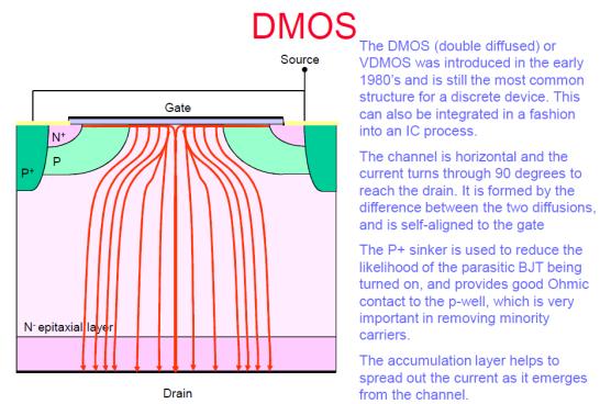
6 Solutions for Silicon Device Trench MOS technology derives from VLSI memory technology The sidewalls are made using dry etching techniques The main advantage is that more cells per unit area can be packed in thus drastically lowering the specific R DS(ON) or package size Another advantage is that the input capacitance can be reduced giving higher switching speeds Finally the Ruggedness of the device is improved; making these devices suitable for harsh environments *VLSI is shorthand for Very Large Scale Integration 11 Switching Characteristic 12 6


7 Trench MOSFET 13 Trench MOSFET 14 7
8 CoolMOS with super junction technology 15 The trench CoolMOS The ultimate power MOS structure combine both superjunction technology and trench technology The trench variant of the CoolMOS could possibly offer even lower onstate voltage drops (especially for low voltage ratings) due to the reduction in the channel resistance and the 1D natural flow of the current 16 8
")
9 IGBT Punch-through (PT) and Non-punch-through (NPT) IGBTs Higher switching rate Negative temperature coefficient Lower on-state voltage drop 17 The Field Stop (or Soft Punch-Through) 18 9


10 The Field Stop, PT and NPT comparison 19 The ultimate IGBT device--superjunction Trench IGBT Superjunction Trench IGBT 20 10
 No established technology at present Other WBG materials like diamond and III/V nitrides suffer from the lack of")
11 Alternatives to Silicon Technology Wide Band Gap Semiconductors Stronger Atomic Bonds Larger breakdown voltage Lower intrinsic carrier concentration SiC Relatively mature technology, native oxide, blue light GaN Poor thermal conductivity, no native oxide, high frequency C (diamond) No established technology at present Other WBG materials like diamond and III/V nitrides suffer from the lack of suitable substrates for epitaxial growth. 21 Physical Properties of Various Semiconductors for Power Devices 22 11

12 Properties of SiC compared to Si 23 Band Gap Electron energy level 24 12


13 Theoretical Limits 25 Power Electronics for Grid Storage 26 13

14 SiC Material What do they look like? 27 What is Silicon Carbide? 28 14

15 History of SiC First observed in 1824 by Jons Jacob Berzelius Acheson process produced an abrasive material LED was made from SiC in 1907 In 1955, Lely presented a new concept of growing high quality crystals 1978, discovery of seeded sublimation growth process by Tairov and Tsvetkov to produce substrates 1987, Cree Research was founded Cree produces 85% of material New producer now entering market 29 SiC Key Technology Problems 30 15

16 SiC Power Devices 31 Example-MOSFET Drift Region 32 16


17 Commercial SiC Diodes 33 Reverse Recovery Comparison 34 17


18 Commercial application 35 SiC PiN Diodes 36 18

19 JBS 37 State of the art SiC Diodes 38 19

20 SiC IGBT Problems of MOSFETs (Channel mobility, reliability) +Problems of Bipolar (current gain, degradation) +Problems of Highly doped P substrate growth September 2006: Cree 10kV P-channel IGBT 3V+20 mω x cm² V F =3.9 V at 10A instead of 4.4V for the VDMOS Improvement of channel mobility and conductivity modulation possible 39 SiC JFETs 40 20

21 SiC JFET state-of-the-art 41 SiC MOSFETs Recent advances in the SiC gate oxidation and device design have enabled the MOSFET to emerge as an attractive transistor for high power switching applications Previous attempts to fabricate 4H-SiC MOSFETs have suffered from poor quality of the silicon dioxide/4h-sic interface This leads to very low inversion channel mobility and large shifts in threshold voltage at elevated temperatures 42 21


22 SiC MOSFETs Unipolar limit 43 Physical Properties: comparison 44 22


23 Applications for GaN-based Devices 45 GaN High Electron Mobility Transistor (HEMT) 46 23

24 GaN HEMTs---Field Plates 47 Heterojunctions: band diagram 48 24

25 Physics of group III-Nitride Piezoelectric Polarization 49 Physics of group III-Nitride Piezoelectric Polarization 50 25

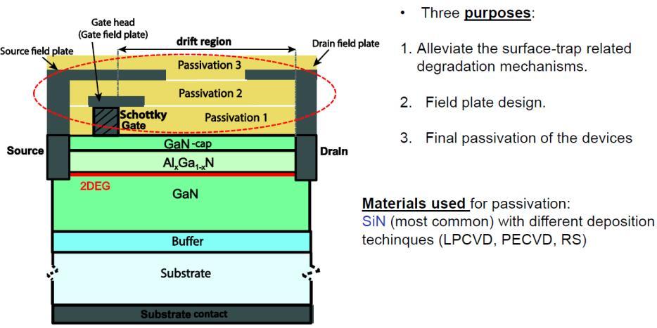
26 2DEG Formation 51 GaN HEMTs---Passivation Layers 52 26


27 GaN HEMTs---AlGaN/GaN heterostructure 53 GaN HEMTs---Buffer 54 27
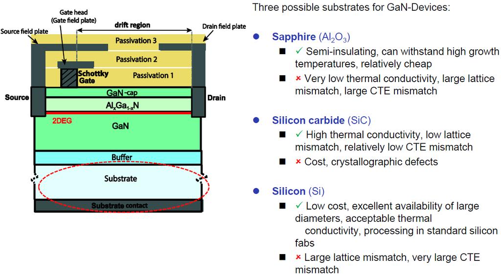
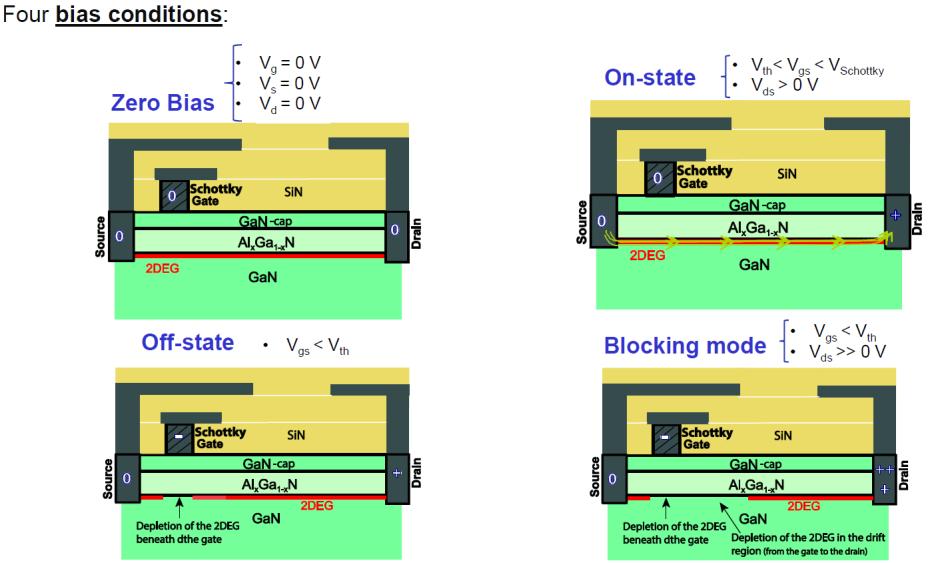
28 GaN HEMTs---Substrate 55 GaN HEMT Operation mode 56 28


29 HEMT Operation mode: Blocking mode 57 E-Mode HEMT (Enhancement mode) 58 29
 MISFET stand for")

30 E-Mode HEMT (Enhancement mode) MISFET stand for Metal Insulation Semiconductor Field Effect Transistor 59 30
Some Key Researches on SiC Device Technologies and their Predicted Advantages
 18 POWER SEMICONDUCTORS www.mitsubishichips.com Some Key Researches on SiC Device Technologies and their Predicted Advantages SiC has proven to be a good candidate as a material for next generation power
Fundamentals of Power Semiconductor Devices
 В. Jayant Baliga Fundamentals of Power Semiconductor Devices 4y Spri ringer Contents Preface vii Chapter 1 Introduction 1 1.1 Ideal and Typical Power Switching Waveforms 3 1.2 Ideal and Typical Power Device
1200 V SiC Super Junction Transistors operating at 250 C with extremely low energy losses for power conversion applications
 1200 V SiC Super Junction Transistors operating at 250 C with extremely low energy losses for power conversion applications Ranbir Singh, Siddarth Sundaresan, Eric Lieser and Michael Digangi GeneSiC Semiconductor,
Power MOSFET Zheng Yang (ERF 3017,
 ECE442 Power Semiconductor Devices and Integrated Circuits Power MOSFET Zheng Yang (ERF 3017, email: yangzhen@uic.edu) Evolution of low-voltage (
Impact of Basal Plane Dislocations and Ruggedness of 10 kv 4H-SiC Transistors
 11th International MOS-AK Workshop (co-located with the IEDM and CMC Meetings) Silicon Valley, December 5, 2018 Impact of Basal Plane Dislocations and Ruggedness of 10 kv 4H-SiC Transistors *, A. Kumar,
How GaN-on-Si can help deliver higher efficiencies in power conversion and power management
 White Paper How GaN-on-Si can help deliver higher efficiencies in power conversion and power management Introducing Infineon's CoolGaN Abstract This paper describes the benefits of gallium nitride on silicon
Power Semiconductor Devices - Silicon vs. New Materials. Si Power Devices The Dominant Solution Today
 Power Semiconductor Devices - Silicon vs. New Materials Jim Plummer Stanford University IEEE Compel Conference July 10, 2017 Market Opportunities for Power Devices Materials Advantages of SiC and GaN vs.
Semiconductor Materials for Power Electronics (SEMPEL) GaN power electronics materials
 GaN power electronics materials") Semiconductor Materials for Power Electronics (SEMPEL) GaN power electronics materials Kjeld Pedersen Department of Physics and Nanotechnology, AAU SEMPEL Semiconductor Materials for Power Electronics
Semiconductor Materials for Power Electronics (SEMPEL) GaN power electronics materials Kjeld Pedersen Department of Physics and Nanotechnology, AAU SEMPEL Semiconductor Materials for Power Electronics
ELEC-E8421 Components of Power Electronics
 ELEC-E8421 Components of Power Electronics MOSFET 2015-10-04 Metal-Oxide-Semiconductor Field-Effect-Transistor (MOSFET) Vertical structure makes paralleling of many small MOSFETs on the chip easy. Very
EE 5611 Introduction to Microelectronic Technologies Fall Thursday, September 04, 2014 Lecture 02
 EE 5611 Introduction to Microelectronic Technologies Fall 2014 Thursday, September 04, 2014 Lecture 02 1 Lecture Outline Review on semiconductor materials Review on microelectronic devices Example of microelectronic
Talk1: Overview of Power Devices and Technology Trends. Talk 2: Devices and Technologies for HVIC
 Talk1: Overview of Power Devices and Technology Trends Talk 2: Devices and Technologies for HVIC Prof. Florin Udrea Cambridge University Taiwan, January 2010 1 Outline Talk 1: Overview of Power Devices
CHAPTER I INTRODUCTION
 CHAPTER I INTRODUCTION High performance semiconductor devices with better voltage and current handling capability are required in different fields like power electronics, computer and automation. Since
Improving Totem-Pole PFC and On Board Charger performance with next generation components
 Improving Totem-Pole PFC and On Board Charger performance with next generation components Anup Bhalla 1) 1) United Silicon Carbide, Inc., 7 Deer Park Drive, Monmouth Jn., NJ USA E-mail: abhalla@unitedsic.com
Gallium nitride (GaN)
") 80 Technology focus: GaN power electronics Vertical, CMOS and dual-gate approaches to gallium nitride power electronics US research company HRL Laboratories has published a number of papers concerning
80 Technology focus: GaN power electronics Vertical, CMOS and dual-gate approaches to gallium nitride power electronics US research company HRL Laboratories has published a number of papers concerning
Safari, Saeed (2015) Impact of silicon carbide device technologies on matrix converter design and performance. PhD thesis, University of Nottingham.
 Impact of silicon carbide device technologies on matrix converter design and performance. PhD thesis, University of Nottingham.") Safari, Saeed (2015) Impact of silicon carbide device technologies on matrix converter design and performance. PhD thesis, University of Nottingham. Access from the University of Nottingham repository:
Safari, Saeed (2015) Impact of silicon carbide device technologies on matrix converter design and performance. PhD thesis, University of Nottingham. Access from the University of Nottingham repository:
Semiconductor Physics and Devices
 Metal-Semiconductor and Semiconductor Heterojunctions The Metal-Oxide-Semiconductor Field-Effect Transistor (MOSFET) is one of two major types of transistors. The MOSFET is used in digital circuit, because
(a) All-SiC 2-in-1 module
 All-SiC 2-in-1 module") All-SiC -in- Module CHONABAYASHI, Mikiya * OTOMO, Yoshinori * KARASAWA, Tatsuya * A B S T R A C T Fuji Electric has developed an utilizing a SiC device that has been adopted in the development of a high-performance
All-SiC -in- Module CHONABAYASHI, Mikiya * OTOMO, Yoshinori * KARASAWA, Tatsuya * A B S T R A C T Fuji Electric has developed an utilizing a SiC device that has been adopted in the development of a high-performance
Advanced Power MOSFET Concepts
 В. Jayant Baliga Advanced Power MOSFET Concepts Springer Contents 1 Introduction 1 1.1 Ideal Power Switching Waveforms 2 1.2 Ideal and Typical Power MOSFET Characteristics 3 1.3 Typical Power MOSFET Structures
Review of Power IC Technologies
 Review of Power IC Technologies Ettore Napoli Dept. Electronic and Telecommunication Engineering University of Napoli, Italy Introduction The integration of Power and control circuitry is desirable for
Power Semiconductors technologies trends for E-Mobility
 1 Power Semiconductors technologies trends for E-Mobility Gianni Vitale Power Conversion & Drives Section Manager System Lab, STMicroelectronics NESEM 2013, Toulouse All trademarks and logos are property
Driving LEDs with SiC MOSFETs
 Power & Energy Efficiency POWERELECTRONICTIPS.COM Driving LEDs with SiC MOSFETs ADAM BARKLEY VIPINDAS PALA SiC Power Device Application Engineer Wolfspeed, a Cree Company Research Scientist Wolfspeed,
All-SiC Modules Equipped with SiC Trench Gate MOSFETs
 All-SiC Modules Equipped with SiC Trench Gate MOSFETs NAKAZAWA, Masayoshi * DAICHO, Norihiro * TSUJI, Takashi * A B S T R A C T There are increasing expectations placed on products that utilize SiC modules
4H-SiC V-Groove Trench MOSFETs with the Buried p + Regions
 ELECTRONICS 4H-SiC V-Groove Trench MOSFETs with the Buried p + Regions Yu SAITOH*, Toru HIYOSHI, Keiji WADA, Takeyoshi MASUDA, Takashi TSUNO and Yasuki MIKAMURA ----------------------------------------------------------------------------------------------------------------------------------------------------------------------------------------------------------------------------------------------------------
IGBT Module Chip Improvements for Industrial Motor Drives
 IGBT Module Chip Improvements for Industrial Motor Drives John F. Donlon Powerex, Inc. 173 Pavilion Lane Youngwood, PA USA Katsumi Satoh Mitsubishi Electric Corporation Power Semiconductor Device Works
21 rue La Noue Bras de Fer Nantes - France Phone : +33 (0) w7-foldite :
 w7-foldite :") 21 rue La Noue Bras de Fer 44200 - Nantes - France Phone : +33 (0) 240 180 916 - email : info@systemplus.fr - w7-foldite : www.systemplus.fr February 2013 Version 1 Written by: Sylvain HALLEREAU DISCLAIMER
21 rue La Noue Bras de Fer 44200 - Nantes - France Phone : +33 (0) 240 180 916 - email : info@systemplus.fr - w7-foldite : www.systemplus.fr February 2013 Version 1 Written by: Sylvain HALLEREAU DISCLAIMER
Comparison of Different Cell Concepts for 1200V- NPT-IGBT's
 Comparison of Different Cell Concepts for 12V- NPT-IGBT's R.Siemieniec, M.Netzel, R. Herzer, D.Schipanski Abstract - IGBT's are relatively new power devices combining bipolar and unipolar properties. In
SuperFAP-G Series of Power MOSFETs
 SuperFAP-G Series of Power s Hiroyuki Tokunishi Tadanori Yamada Masanori Inoue 1. Introduction In recent years, shipments of information and communication equipment, mainly network related equipment such
MOSFET & IC Basics - GATE Problems (Part - I)
") MOSFET & IC Basics - GATE Problems (Part - I) 1. Channel current is reduced on application of a more positive voltage to the GATE of the depletion mode n channel MOSFET. (True/False) [GATE 1994: 1 Mark]
MOSFET & IC Basics - GATE Problems (Part - I) 1. Channel current is reduced on application of a more positive voltage to the GATE of the depletion mode n channel MOSFET. (True/False) [GATE 1994: 1 Mark]
A new Vertical JFET Technology for Harsh Radiation Applications
 A New Vertical JFET Technology for Harsh Radiation Applications ISPS 2016 1 A new Vertical JFET Technology for Harsh Radiation Applications A Rad-Hard switch for the ATLAS Inner Tracker P. Fernández-Martínez,
Customized probe card for on-wafer testing of AlGaN/GaN power transistors
 Customized probe card for on-wafer testing of AlGaN/GaN power transistors R. Venegas 1, K. Armendariz 2, N. Ronchi 1 1 imec, 2 Celadon Systems Inc. Outline Introduction GaN for power switching applications
Introduction Device Achievements & Needs Future Prospects of SiC Power Devices Conclusion
 Present Present Status Status And And Future Future Prospects of of SiC SiC Power Power Devices Devices Contributors : Gourab Majumdar Chief Engineer, Power Device Works, Mitsubishi Electric Corporation,
Power Semiconductors Key Enablers for Energy Efficiency
 Power Semiconductors Key Enablers for Energy Efficiency Oliver Häberlen Senior Principal Technology Development Infineon Technologies Austria AG, 9500 Villach, Austria Introduction The world wide increase
Power Matters Microsemi SiC Products
 Microsemi SiC Products James Kerr Director of Marketing Power Discrete Products Microsemi Power Products MOSFETs (100V-1200V) Highest Performance SiC MOSFETs 1200V MOSFETs FREDFETs (MOSFET with fast body
Progress Energy Distinguished University Professor Jay Baliga. April 11, Acknowledgements
 Progress Energy Distinguished University Professor Jay Baliga April 11, 2019 Acknowledgements 1 Outline SiC Power MOSFET Breakthroughs achieved at NCSU PRESiCE: SiC Power Device Manufacturing Technology
Design considerations for chargecompensated. medium-voltage range. Ralf Siemieniec, Cesar Braz, Oliver Blank Infineon Technologies Austria AG
 Design considerations for chargecompensated power MOSFET in the medium-voltage range Ralf Siemieniec, Cesar Braz, Oliver Blank Infineon Technologies Austria AG Outline 1 Introduction 2 Application requirements
PHYSICS OF SEMICONDUCTOR DEVICES
 PHYSICS OF SEMICONDUCTOR DEVICES PHYSICS OF SEMICONDUCTOR DEVICES by J. P. Colinge Department of Electrical and Computer Engineering University of California, Davis C. A. Colinge Department of Electrical
Customized probe card for on wafer testing of AlGaN/GaN power transistors
 Customized probe card for on wafer testing of AlGaN/GaN power transistors R. Venegas 1, K. Armendariz 2, N. Ronchi 1 1 imec, 2 Celadon Systems Inc. Presented by Bryan Root 2 Outline Introduction GaN for
CONTENTS. 2.2 Schrodinger's Wave Equation 31. PART I Semiconductor Material Properties. 2.3 Applications of Schrodinger's Wave Equation 34
 CONTENTS Preface x Prologue Semiconductors and the Integrated Circuit xvii PART I Semiconductor Material Properties CHAPTER 1 The Crystal Structure of Solids 1 1.0 Preview 1 1.1 Semiconductor Materials
T-series and U-series IGBT Modules (600 V)
") T-series and U-series IGBT Modules (6 V) Seiji Momota Syuuji Miyashita Hiroki Wakimoto 1. Introduction The IGBT (insulated gate bipolar transistor) module is the most popular power device in power electronics
T-series and U-series IGBT Modules (6 V) Seiji Momota Syuuji Miyashita Hiroki Wakimoto 1. Introduction The IGBT (insulated gate bipolar transistor) module is the most popular power device in power electronics
Design and Optimization of Superjunction Vertical DMOS Power Transistors using Sentaurus Device Simulation
 University of Central Florida Electronic Theses and Dissertations Masters Thesis (Open Access) Design and Optimization of Superjunction Vertical DMOS Power Transistors using Sentaurus Device Simulation
International Workshop on Nitride Semiconductors (IWN 2016)
") International Workshop on Nitride Semiconductors (IWN 2016) Sheng Jiang The University of Sheffield Introduction The 2016 International Workshop on Nitride Semiconductors (IWN 2016) conference is held
International Workshop on Nitride Semiconductors (IWN 2016) Sheng Jiang The University of Sheffield Introduction The 2016 International Workshop on Nitride Semiconductors (IWN 2016) conference is held
Solid State Device Fundamentals
 Solid State Device Fundamentals 4.4. Field Effect Transistor (MOSFET) ENS 463 Lecture Course by Alexander M. Zaitsev alexander.zaitsev@csi.cuny.edu Tel: 718 982 2812 4N101b 1 Field-effect transistor (FET)
ENHANCING POWER ELECTRONIC DEVICES WITH WIDE BANDGAP SEMICONDUCTORS
 ENHANCING POWER ELECTRONIC DEVICES WITH WIDE BANDGAP SEMICONDUCTORS BURAK OZPINECI Oak Ridge National Laboratory Oak Ridge, TN 37831-6472 USA ozpinecib@ornl.gov MADHU SUDHAN CHINTHAVALI Oak Ridge Institute
Temperature-Dependent Characterization of SiC Power Electronic Devices
 Temperature-Dependent Characterization of SiC Power Electronic Devices Madhu Sudhan Chinthavali 1 chinthavalim@ornl.gov Burak Ozpineci 2 burak@ieee.org Leon M. Tolbert 2, 3 tolbert@utk.edu 1 Oak Ridge
Characterization and Modeling of 4H-SiC Low Voltage MOSFETs and Power MOSFETs
 University of Arkansas, Fayetteville ScholarWorks@UARK Theses and Dissertations 5-2012 Characterization and Modeling of 4H-SiC Low Voltage MOSFETs and Power MOSFETs Mihir Mudholkar University of Arkansas,
SiC Cascodes and its advantages in power electronic applications
 SiC Cascodes and its advantages in power electronic applications WBG Power Conference, Munich, 5 th December 2017 Christopher Rocneanu Director Sales Europe and North America cro@unitedsic.com +4915121063411
Study on Fabrication and Fast Switching of High Voltage SiC JFET
 Advanced Materials Research Online: 2013-10-31 ISSN: 1662-8985, Vol. 827, pp 282-286 doi:10.4028/www.scientific.net/amr.827.282 2014 Trans Tech Publications, Switzerland Study on Fabrication and Fast Switching
MOSFET Modeling, Simulation and Parameter Extraction in 4H- and 6H- Silicon Carbide
 University of Tennessee, Knoxville Trace: Tennessee Research and Creative Exchange Doctoral Dissertations Graduate School 5-2005 MOSFET Modeling, Simulation and Parameter Extraction in 4H- and 6H- Silicon
Semiconductor Physics and Devices
 Nonideal Effect The experimental characteristics of MOSFETs deviate to some degree from the ideal relations that have been theoretically derived. Semiconductor Physics and Devices Chapter 11. MOSFET: Additional
GaN: Applications: Optoelectronics
 GaN: Applications: Optoelectronics GaN: Applications: Optoelectronics - The GaN LED industry is >10 billion $ today. - Other optoelectronic applications of GaN include blue lasers and UV emitters and detectors.
The Next Generation of Power Conversion Systems Enabled by SiC Power Devices
 Innovations Embedded The Next Generation of Power Conversion Systems Enabled by SiC Power Devices White Paper The world has benefitted from technology innovations and continued advancements that have contributed
value of W max for the device. The at band voltage is -0.9 V. Problem 5: An Al-gate n-channel MOS capacitor has a doping of N a = cm ;3. The oxi
 Prof. Jasprit Singh Fall 2001 EECS 320 Homework 10 This homework is due on December 6 Problem 1: An n-type In 0:53 Ga 0:47 As epitaxial layer doped at 10 16 cm ;3 is to be used as a channel in a FET. A
INTRODUCTION: Basic operating principle of a MOSFET:
 INTRODUCTION: Along with the Junction Field Effect Transistor (JFET), there is another type of Field Effect Transistor available whose Gate input is electrically insulated from the main current carrying
Semiconductor Devices
 Semiconductor Devices Modelling and Technology Source Electrons Gate Holes Drain Insulator Nandita DasGupta Amitava DasGupta SEMICONDUCTOR DEVICES Modelling and Technology NANDITA DASGUPTA Professor Department
ECE520 VLSI Design. Lecture 2: Basic MOS Physics. Payman Zarkesh-Ha
 ECE520 VLSI Design Lecture 2: Basic MOS Physics Payman Zarkesh-Ha Office: ECE Bldg. 230B Office hours: Wednesday 2:00-3:00PM or by appointment E-mail: pzarkesh@unm.edu Slide: 1 Review of Last Lecture Semiconductor
Integrated diodes. The forward voltage drop only slightly depends on the forward current. ELEKTRONIKOS ĮTAISAI
 1 Integrated diodes pn junctions of transistor structures can be used as integrated diodes. The choice of the junction is limited by the considerations of switching speed and breakdown voltage. The forward
Department of Electrical Engineering IIT Madras
 Department of Electrical Engineering IIT Madras Sample Questions on Semiconductor Devices EE3 applicants who are interested to pursue their research in microelectronics devices area (fabrication and/or
Power Devices and ICs Chapter 15
 Power Devices and ICs Chapter 15 Syed Asad Alam DA, ISY 4/28/2015 1 Overview 4/28/2015 2 Overview Types of Power Devices PNPN Thyristor TRIAC (Triode Alternating Current) GTO (Gate Turn-Off Thyristor)
Difference between BJTs and FETs. Junction Field Effect Transistors (JFET)
") Difference between BJTs and FETs Transistors can be categorized according to their structure, and two of the more commonly known transistor structures, are the BJT and FET. The comparison between BJTs
Difference between BJTs and FETs Transistors can be categorized according to their structure, and two of the more commonly known transistor structures, are the BJT and FET. The comparison between BJTs
Power Bipolar Junction Transistors (BJTs)
") ECE442 Power Semiconductor Devices and Integrated Circuits Power Bipolar Junction Transistors (BJTs) Zheng Yang (ERF 3017, email: yangzhen@uic.edu) Power Bipolar Junction Transistor (BJT) Background The
ECE442 Power Semiconductor Devices and Integrated Circuits Power Bipolar Junction Transistors (BJTs) Zheng Yang (ERF 3017, email: yangzhen@uic.edu) Power Bipolar Junction Transistor (BJT) Background The
ELECTRONIC DEVICES AND CIRCUITS
 ELECTRONIC DEVICES AND CIRCUITS 1. At room temperature the current in an intrinsic semiconductor is due to A. holes B. electrons C. ions D. holes and electrons 2. Work function is the maximum energy required
DEVELOPMENT OF 4H SILICON CARBIDE JFET-BASED POWER INTEGRATED CIRCUITS YONGXI ZHANG. A Dissertation submitted to the Graduate School-New Brunswick
 DEVELOPMENT OF 4H SILICON CARBIDE JFET-BASED POWER INTEGRATED CIRCUITS by YONGXI ZHANG A Dissertation submitted to the Graduate School-New Brunswick Rutgers, The State University of New Jersey In partial
Evolution of SiC MOSFETs at Cree Performance and Reliability
 Evolution of SiC MOSFETs at Cree Performance and Reliability Brett Hull :: August 13, 2015 Dan Lichtenwalner, Vipin Pala, Edward VanBrunt, Sei- Hyung Ryu, Jim Richmond, Leo Wang, Philip Butler, Don Gajewski,
Lesson 5. Electronics: Semiconductors Doping p-n Junction Diode Half Wave and Full Wave Rectification Introduction to Transistors-
 Lesson 5 Electronics: Semiconductors Doping p-n Junction Diode Half Wave and Full Wave Rectification Introduction to Transistors- Types and Connections Semiconductors Semiconductors If there are many free
Advanced Silicon Devices Applications and Technology Trends
 Advanced Silicon Devices Applications and Technology Trends Gerald Deboy Winfried Kaindl, Uwe Kirchner, Matteo Kutschak, Eric Persson, Michael Treu APEC 2015 Content Silicon devices versus GaN devices:
Chapter 3: Basics Semiconductor Devices and Processing 2006/9/27 1. Topics
 Chapter 3: Basics Semiconductor Devices and Processing 2006/9/27 1 Topics What is semiconductor Basic semiconductor devices Basics of IC processing CMOS technologies 2006/9/27 2 1 What is Semiconductor
Power MOSFET Basics: Understanding Superjunction Technology
 Originally developed for EDN. For more related features, blogs and insight from the EE community, go to www.edn.com Power MOSFET Basics: Understanding Superjunction Technology Sanjay Havanur and Philip
Three Terminal Devices
 Three Terminal Devices - field effect transistor (FET) - bipolar junction transistor (BJT) - foundation on which modern electronics is built - active devices - devices described completely by considering
Normally-Off Operation of AlGaN/GaN Heterojunction Field-Effect Transistor with Clamping Diode
 JOURNAL OF SEMICONDUCTOR TECHNOLOGY AND SCIENCE, VOL.16, NO.2, APRIL, 2016 ISSN(Print) 1598-1657 http://dx.doi.org/10.5573/jsts.2016.16.2.221 ISSN(Online) 2233-4866 Normally-Off Operation of AlGaN/GaN
Fig. 1 - Enhancement mode GaN has a circuiut schematic similar to silicon MOSFETs with Gate (G), Drain (D), and Source (S).
, Drain (D), and Source (S).") GaN Basics: FAQs Sam Davis; Power Electronics Wed, 2013-10-02 Gallium nitride transistors have emerged as a high-performance alternative to silicon-based transistors, thanks to the technology's ability
GaN Basics: FAQs Sam Davis; Power Electronics Wed, 2013-10-02 Gallium nitride transistors have emerged as a high-performance alternative to silicon-based transistors, thanks to the technology's ability
A new compact power modules range for efficient solar inverters
 A new compact power modules range for efficient solar inverters Serge Bontemps, Pierre-Laurent Doumergue Microsemi PPG power module Products, Chemin de Magret, F-33700 Merignac Abstract The decrease of
Wide Band-Gap (SiC and GaN) Devices Characteristics and Applications. Richard McMahon University of Cambridge
 Devices Characteristics and Applications. Richard McMahon University of Cambridge") Wide Band-Gap (SiC and GaN) Devices Characteristics and Applications Richard McMahon University of Cambridge Wide band-gap power devices SiC : MOSFET JFET Schottky Diodes Unipolar BJT? Bipolar GaN : FET
Wide Band-Gap (SiC and GaN) Devices Characteristics and Applications Richard McMahon University of Cambridge Wide band-gap power devices SiC : MOSFET JFET Schottky Diodes Unipolar BJT? Bipolar GaN : FET
Comparison of SiC and Si Power Semiconductor Devices to Be Used in 2.5 kw DC/DC Converter
 Comparison of SiC and Si Power Semiconductor Devices to Be Used in 2.5 kw DC/DC Converter M. G. Hosseini Aghdam Division of Electric Power Engineering Department of Energy and Environment Chalmers University
Lecture 19 Real Semiconductor Switches and the Evolution of Power MOSFETS A.. Real Switches: I(D) through the switch and V(D) across the switch
 through the switch and V(D) across the switch") Lecture 19 Real Semiconductor Switches and the Evolution of Power MOSFETS 1 A.. Real Switches: I(D) through the switch and V(D) across the switch 1. Two quadrant switch implementation and device choice
Lecture 19 Real Semiconductor Switches and the Evolution of Power MOSFETS 1 A.. Real Switches: I(D) through the switch and V(D) across the switch 1. Two quadrant switch implementation and device choice
Unit III FET and its Applications. 2 Marks Questions and Answers
 Unit III FET and its Applications 2 Marks Questions and Answers 1. Why do you call FET as field effect transistor? The name field effect is derived from the fact that the current is controlled by an electric
Wide Band Gap Power Semiconductor Devices and their Applications
 Bilal Ahmad Wide Band Gap Power Semiconductor Devices and their Applications School of Electrical Engineering Master s Thesis submitted in partial fulfilment of the requirement for the degree of Master
EDC UNIT IV- Transistor and FET Characteristics EDC Lesson 9- ", Raj Kamal, 1
 EDC UNIT IV- Transistor and FET Characteristics Lesson-9: JFET and Construction of JFET 2008 EDC Lesson 9- ", Raj Kamal, 1 1. Transistor 2008 EDC Lesson 9- ", Raj Kamal, 2 Transistor Definition The transferred-resistance
Study of Static and Dynamic Characteristics of Silicon and Silicon Carbide Devices
 Study of Static and Dynamic Characteristics of Silicon and Silicon Carbide Devices Sreenath S Dept. of Electrical & Electronics Engineering Manipal University Jaipur Jaipur, India P. Ganesan External Guide
ADVANCED POWER RECTIFIER CONCEPTS
 ADVANCED POWER RECTIFIER CONCEPTS B. Jayant Baliga ADVANCED POWER RECTIFIER CONCEPTS B. Jayant Baliga Power Semiconductor Research Center North Carolina State University Raleigh, NC 27695-7924, USA bjbaliga@unity.ncsu.edu
USING F-SERIES IGBT MODULES
 .0 Introduction Mitsubishi s new F-series IGBTs represent a significant advance over previous IGBT generations in terms of total power losses. The device remains fundamentally the same as a conventional
Gallium Nitride (GaN) Technology Overview
 Technology Overview") The following chapter is from the First Edition of "GaN Transistors for Efficient Power Conversion" Purchase Second Edition CHAPTER 1: Gallium Nitride (GaN) Technology Overview Silicon Power MOSFETs from
The following chapter is from the First Edition of "GaN Transistors for Efficient Power Conversion" Purchase Second Edition CHAPTER 1: Gallium Nitride (GaN) Technology Overview Silicon Power MOSFETs from
Pitch Pack Microsemi full SiC Power Modules
 Pitch Pack Microsemi full SiC Power Modules October 2014 SiC Main Characteristics vs. Si Characteristics SiC vs. Si Results Benefits Breakdown field (MV/cm) Electron sat. velocity (cm/s) Bandgap energy
EE70 - Intro. Electronics
 EE70 - Intro. Electronics Course website: ~/classes/ee70/fall05 Today s class agenda (November 28, 2005) review Serial/parallel resonant circuits Diode Field Effect Transistor (FET) f 0 = Qs = Qs = 1 2π
Today s subject MOSFET and IGBT
 Today s subject MOSFET and IGBT 2018-05-22 MOSFET metal oxide semiconductor field effect transistor Drain Gate n-channel Source p-channel The MOSFET - Source Gate G D n + p p n + S body body n - drift
Solid State Devices- Part- II. Module- IV
 Solid State Devices- Part- II Module- IV MOS Capacitor Two terminal MOS device MOS = Metal- Oxide- Semiconductor MOS capacitor - the heart of the MOSFET The MOS capacitor is used to induce charge at the
Analysis of Lattice Temperature in Super Junction Trench Gate Power MOSFET as Changing Degree of Trench Etching
 JOURNAL OF SEMICONDUCTOR TECHNOLOGY AND SCIENCE, VOL.14, NO.3, JUNE, 2014 http://dx.doi.org/10.5573/jsts.2014.14.3.263 Analysis of Lattice Temperature in Super Junction Trench Gate Power MOSFET as Changing
Power Semiconductor Devices
 TRADEMARK OF INNOVATION Power Semiconductor Devices Introduction This technical article is dedicated to the review of the following power electronics devices which act as solid-state switches in the circuits.
SiC Transistor Basics: FAQs
 SiC Transistor Basics: FAQs Silicon Carbide (SiC) MOSFETs exhibit higher blocking voltage, lower on state resistance and higher thermal conductivity than their silicon counterparts. Oct. 9, 2013 Sam Davis
Appendix: Power Loss Calculation
 Appendix: Power Loss Calculation Current flow paths in a synchronous buck converter during on and off phases are illustrated in Fig. 1. It has to be noticed that following parameters are interrelated:
GaN power electronics
 GaN power electronics The MIT Faculty has made this article openly available. Please share how this access benefits you. Your story matters. Citation As Published Publisher Lu, Bin, Daniel Piedra, and
Testing modern Silicon Carbide MOSFET devices against short-circuit
 MSc. Thesis Testing modern Silicon Carbide MOSFET devices against short-circuit Pablo Rodriguez de Mora PED 141 supervised by Lorenzo Ceccarelli 1, Paula Diaz Reigosa 1 and Francesco Iannuzzo 1 1 Aalborg
USCi MOSFET progress (ARL HVPT program)
") USCi MOSFET progress (ARL HVPT program) L. Fursin, X. Huang, W. Simon, M. Fox, J. Hostetler, X. Li, A. Bhalla Aug 18, 2016 Contents USCi product line 1200V MOSFET progress 10kV IGBT and MPS progress 2
USCi MOSFET progress (ARL HVPT program) L. Fursin, X. Huang, W. Simon, M. Fox, J. Hostetler, X. Li, A. Bhalla Aug 18, 2016 Contents USCi product line 1200V MOSFET progress 10kV IGBT and MPS progress 2
Chapter 3 Basics Semiconductor Devices and Processing
 Chapter 3 Basics Semiconductor Devices and Processing 1 Objectives Identify at least two semiconductor materials from the periodic table of elements List n-type and p-type dopants Describe a diode and
Chapter 9 SiC Planar MOSFET Structures
 Chapter 9 SiC Planar MOSFET Structures In Chap. 1, it was demonstrated that the specific on-resistance of power MOSFET devices can be greatly reduced by replacing silicon with wide band gap semiconductors.
High-Temperature and High-Frequency Performance Evaluation of 4H-SiC Unipolar Power Devices
 High-Temperature and High-Frequency Performance Evaluation of H-SiC Unipolar Power Devices Madhu Sudhan Chinthavali Oak Ridge Institute for Science and Education Oak Ridge, TN 37831-117 USA chinthavalim@ornl.gov
L MOSFETS, IDENTIFICATION, CURVES. PAGE 1. I. Review of JFET (DRAW symbol for n-channel type, with grounded source)
") L.107.4 MOSFETS, IDENTIFICATION, CURVES. PAGE 1 I. Review of JFET (DRAW symbol for n-channel type, with grounded source) 1. "normally on" device A. current from source to drain when V G = 0 no need to
L.107.4 MOSFETS, IDENTIFICATION, CURVES. PAGE 1 I. Review of JFET (DRAW symbol for n-channel type, with grounded source) 1. "normally on" device A. current from source to drain when V G = 0 no need to
NAME: Last First Signature
 UNIVERSITY OF CALIFORNIA, BERKELEY College of Engineering Department of Electrical Engineering and Computer Sciences EE 130: IC Devices Spring 2003 FINAL EXAMINATION NAME: Last First Signature STUDENT
(Original signatures are on file with official student records.)
") To the Graduate Council: I am submitting herewith a dissertation written by Hui Zhang entitled Electro-Thermal Modeling of SiC Power Electronic Systems. I have examined the final electronics copy of this
To the Graduate Council: I am submitting herewith a dissertation written by Hui Zhang entitled Electro-Thermal Modeling of SiC Power Electronic Systems. I have examined the final electronics copy of this
Power Semiconductor Devices for Variable Frequency Drives
 B. Jayant Baliga Chapter 1 Power Semiconductor Devices for Variable Frequency Drives 1.1. INTRODUCTION Improvements in the performance of variable frequency drives have been directly related to the availability
UNIT 3 Transistors JFET
 UNIT 3 Transistors JFET Mosfet Definition of BJT A bipolar junction transistor is a three terminal semiconductor device consisting of two p-n junctions which is able to amplify or magnify a signal. It