Advances in Averaged Switch Modeling
|
|
|
- Donna Davidson
- 5 years ago
- Views:
Transcription
1 Advances in Averaged Switch Modeling Robert W. Erickson Power Electronics Group University of Colorado Boulder, Colorado USA
2 Outline of tutorial presentation 1. Introduction: Objectives of converter modeling via averaged switch approach 2. Averaged switch modeling of PWM converters operating in continuous conduction mode 2.1 Basics of averaged switch modeling 2.2 Modeling switching loss 2.3 Modeling converter dynamics 3. Discontinuous conduction mode in PWM converters 3.1 Averaged switch model 3.2 Properties of the dependent power source 3.3 Solution of converter characteristics 3.4 Modeling converter dynamics 2
3 Outline of tutorial presentation continued 4. Current programmed control of PWM converters 4.1 Averaged switch model, CCM 4.2 Ac model, CCM 4.3 DCM models 5. Single-phase low-harmonic rectifiers 5.1 The ideal rectifier 5.2 Integrated High-Quality Rectifier-Regulators 6. Single-switch three-phase low-harmonic rectifiers 6.1 The ideal 3ø rectifier 6.2 Single-switch approaches to three-phase rectification 7. Summary 3
4 1. Introduction Objectives of converter modeling via the averaged switch approach 4
5
6 Objectives of converter modeling Dc-dc converter system: modeling of efficiency and losses Boost converter example i L i C Develop loss model Solve for steady-state losses and efficiency V g DT s T s C R v Specify component requirements such that efficiency specifications are met Steady-state model R L DRon D'V D D'R D D' : 1 V g I V R 5
7 Objectives of converter modeling Dc-dc converter system: modeling of dynamics Develop block diagram of system Determine the relevant small-signal transfer functions Control-to-output Disturbance-to-output Design system to meet specifications Reference input Error signal Compensator G c (s) Pulse-width modulator ac line variation Duty cycle variation G vg (s) G vd (s) Z out (s) Load current variation Converter power stage Output voltage variation H(s) Sensor gain 6
8 Objectives of converter modeling Ac-dc low-harmonic rectifier system: efficiency and losses Boost rectifier example i g i ac v ac v g R L L Controller Q 1 D 1 i d C i v R Develop loss model Solve for steady-state losses and efficiency Specify component requirements such that efficiency specifications are met Low-frequency averaged model η i g R L dr on d' : 1 V F i d i = I 0.9 v g C R (Large) v = V V M /V 7
9 Objectives of converter modeling Ac-dc low-harmonic rectifier system: dynamic modeling v ac i g i ac v g Boost converter L D 1 Q 1 i 2 v C C DCDC Converter i Load v v control Multiplier X v g R s i g v a PWM d v v ref1 = k x v g v control v err G c (s) Compensator Compensator and modulator v ref3 Wide-bandwidth input current controller Wide-bandwidth output voltage controller Model inner and outer loops of rectifier control system Design to meet specifications v C Compensator v ref2 Low-bandwidth energy-storage capacitor voltage controller 8
10
11 Averaged switch modeling Switch network is replaced by averaged circuit model. Switching harmonics are removed, and low-frequency components of waveforms are modeled in a simple way. A very general approach to modeling converter losses, efficiency, and dynamics. Easily taught to students. Yields an intuitive understanding of converter behavior in CCM, DCM, current-programmed mode, etc. Results are easy to generalize to other converters. Well-suited to simulation using PSPICE. Applicable to dc-dc converters, as well as dc-ac inverters, ac-dc low-harmonic rectifiers, ac-ac matrix converters. 9
12 2. Averaged switch modeling of PWM converters operating in the continuous conduction mode 2.1 Basics of averaged switch modeling 2.2 Modeling switching loss 2.3 Modeling converter dynamics 10
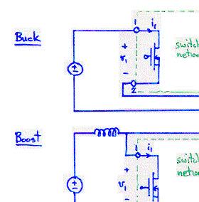
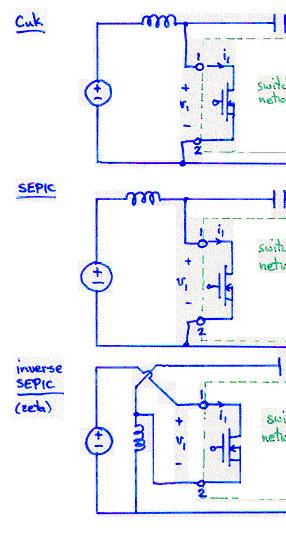
13 2.1. Averaged switch modeling Basic approach Given a PWM converter operating in continuous conduction mode: L 1 C 1 D 1 V g L 2 C 2 R v SEPIC example Q 1 Separate the switching elements from the remainder of the converter... 11
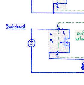
14 Definition of switch network, SEPIC example Define a switch network, containing all of the converter switching elements. The remainder of the converter is linear and timeinvariant. The terminal voltages and currents of the switch network can be arbitrarily defined. v g i L1 L 1 i 1 v 1 C 1 v C1 Q 1 L 2 i L2 Switch network Duty cycle D 1 d v 2 i 2 C 2 v C2 R 12
15 Switching converter system with switch network explicitly defined Power input Time-invariant network containing converter reactive elements Load v g C L R v v C i L i 1 v 1 Switch network i 2 v 2 Control input d 13
16 Discussion The number of ports in the switch network is less than or equal to the number of SPST switches in the converter Simple dc-dc case, in which converter contains two SPST switches: switch network contains two ports The switch network terminal waveforms are then the port voltages and currents: v 1, i 1, v 2, and i 2. Two of these waveforms can be taken as independent inputs to the switch network; the remaining two waveforms are then viewed as dependent outputs of the switch network. Switch network also includes control input d Definition of the switch network terminal quantities is not unique. Different definitions lead equivalent results having different forms 14
17 A few points regarding averaged switch modeling The switch network can be defined arbitrarily, as long as its terminal voltages and currents are independent, and the switch network contains no reactive elements. It is not necessary that some of the switch network terminal quantities coincide with inductor currents or capacitor voltages of the converter, or be nonpulsating. The object is simply to write the averaged equations of the switch network; i.e., to express the average values of half of the switch network terminal waveforms as functions of the average values of the remaining switch network terminal waveforms, and the control input. 15
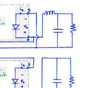
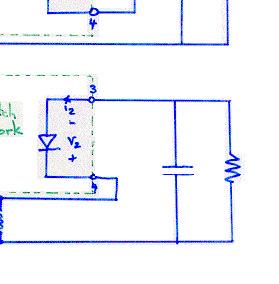
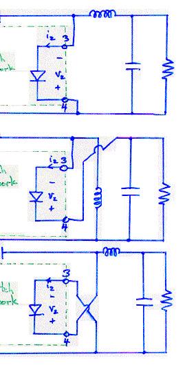
18 Terminal waveforms of the switch network v 1 v C1 v C2 L 1 C dt s T s t v g i L1 v C1 L 2 C 2 v C2 R i 1 i L1 i L2 i L dt s v 2 v C1 v C2 T s t i 1 v 1 Switch network Q 1 D 1 v 2 i dt s T s t Duty cycle d i 2 i L1 i L dt s T s t 16
19 The averaging step x Ts = 1 T s t t Ts xdt Now average all waveforms over one switching period: Power input Averaged time-invariant network containing converter reactive elements Load v g Ts C L R v Ts v C Ts i L Ts i 1 Ts i 2 Ts v 1 Ts Averaged switch network v 2 Ts Control input d 17
20 The averaging step The basic assumption is made that the natural time constants of the converter are much longer than the switching period, so that the converter contains low-pass filtering of the switching harmonics: One may average the waveforms over an interval that is short compared to the system natural time constants, without significantly altering the system response. In particular, averaging over the switching period T s removes the switching harmonics, while preserving the low-frequency components of the waveforms. This step removes the small but mathematically-complicated switching harmonics, leading to a relatively simple and tractable converter model. In practice, the only work needed for this step is to average the switch dependent waveforms. 18
21 Averaged terminal equations of the switch network (small switching ripple is neglected) v 1 v C1 v C2 v 2 v C1 v C dt s T s t dt s T s t i 1 i L1 i L2 i 2 i L1 i L dt s T s t dt s T s t 19
22 Derivation of switch network equations (Algebra steps) We can write Result i 1 Ts v 1 Ts v 2 Ts Hence i 2 Ts Averaged switch network Modeling the switch network via averaged dependent sources 20
23
24 Steady-state switch model: Dc transformer model Original switch network i 1 Switch network i 2 v 1 Q 1 D 1 v 2 Averaged steady-state model: DC transformer Correctly represents the relationships between the dc and low-frequency components of the terminal waveforms of the switch network V 1 I 1 Duty cycle d D' : D I 2 V 2 21
25 Steady-state CCM SEPIC model Replace switch network with dc transformer model L 1 C 1 I L1 V C1 V g L 2 C 2 V C2 R I L2 I 1 V 1 D' : D V 2 Can now let inductors become short circuits, capacitors become open circuits, and solve for dc conditions. I 2 Can simulate this model using PSPICE, to find transient waveforms 22
26 The ideal dc transformer model Switch network Averaged switch model i 1 i 2 1 : d CCM v 1 v 2 Correctly represents the basic properties of the ideal CCM PWM switch network: 100% efficiency Voltage and current conversion ratios, controllable by duty cycle d 23
27
28
29 Several ways to define the PWM switch network, and the corresponding CCM models i 1 i 2 i 1 Ts 1 : D i 2 Ts v 1 v 2 v 1 Ts v 2 Ts i 1 i 2 i 1 Ts D' : 1 i 2 Ts v 1 v 2 v 1 Ts v 2 Ts i 1 i 2 i 1 Ts D' : D i 2 Ts v 1 v 2 v 1 Ts v 2 Ts 24
30 PSPICE simulation of the dc transformer model Use dependent sources: Switch network Averaged switch model PSPICE switch model i 1 i 2 1 : d v 1 v 2 d i 2 Ts d v 1 T s Polynomial dependent sources can be used to simulate the terminal equations of the ideal dc transformer model 25
31 2.2. Modeling switching loss Example: diode stored charge in boost converter i L L i 1 i 2 v g v 1 v 2 C R v v 1 Waveforms: v 2 v 2 i 2 t r 0 dt s T s 0 t Other switching loss mechanisms are ignored in this example; one can include other losses if desired, using a similar procedure i 1 i 1 Determine averaged terminal waveforms of switch network 0 0 t Construct averaged equivalent circuit model Area Q r 26
32 Expressions for average terminal waveforms Boost converter, switching loss example v 1 v 1 T s = 1 T s t r (1 d)t s v 2 Ts v 2 v 2 i 2 Ts = 1 T s Q r i 1 Ts t r (1 d)t s t r = diode reverse recovery time Q r = diode recovered charge i 2 i 1 t r 0 dt s T s 0 i 1 t 0 0 t Area Q r 27
33 Averaged equivalent circuit of switch network v 1 Ts = t r T s (1 d) v 2 Ts i 2 Ts = Q r T s t r T s (1 d) i 1 T s i 1 i 2 i 1 Ts i 2 Ts v 1 v 2 v 1 Ts v 2 Ts Diode reverse recovery time affects conversion ratio Stored charge leads to power loss, modeled by current sink 28
34 Insert averaged switch model into converter circuit Original converter v g i L L i 1 v 1 i 2 v 2 C R v Averaged model v g Ts i L Ts L i 1 Ts i 2 Ts v 1 Ts v 2 Ts C R v Ts Steadystate solution: 29
35
36 2.3. Modeling converter dynamics: Small-signal linearization of model Perturb and linearize the switch network averaged waveforms about a quiescent operating point. Let: Voltage equation becomes Eliminate nonlinear terms and solve for v 1 terms: 30
37 Linearization, continued Current equation becomes Eliminate nonlinear terms and solve for i 2 terms: 31
38
39 Switch network: Small-signal ac model Reconstruct an equivalent circuit that corresponds to these smallsignal equations: D' : D Transistor port Diode port A general small-signal ac model for the PWM switch network operating in CCM. 32
40 Small-signal ac model of the CCM SEPIC Replace switch network with small-signal ac model: L 1 C 1 L 2 C 2 R D' : D Can now solve this model to determine ac transfer functions 33
41
42 Small-signal models of several basic switch networks i 1 i 2 1 : D v 1 v 2 i 1 i 2 D' : 1 v 1 v 2 i 1 i 2 D' : D v 1 v 2 34
43 Table of results Transfer functions of the basic buck, boost, and buck-boost converters Control-to-output and line-to-output transfer functions G vd (s) and G vg (s) Converter G g0 G d0 ω 0 Q ω z V 1 buck D D R C LC L 1 V D' boost D' D' D'R C D' 2 R LC L L buck-boost D' D V D' D D' 2 D'R C D' 2 R LC L D L where the transfer functions are written in the standard forms 35
44 3. Discontinuous conduction mode in PWM converters 3.1 Averaged switch model 3.2 Properties of the dependent power source 3.3 Solution of averaged model 3.4 Modeling converter dynamics 36
45 Equivalent circuit modeling of discontinuous conduction mode converters DC AC 1 : M(D) 1 : M(D) L e CCM V g R V C R DCM V g? R V? R 37
46 Change in characteristics at the CCM/DCM boundary Steady-state output voltage becomes strongly load-dependent Simpler dynamics: one pole and the RHP zero are moved to very high frequency, and can normally be ignored Traditionally, boost and buck-boost converters are designed to operate in DCM at full load All converters may operate in DCM at light load So we need equivalent circuits that model the steady-state and smallsignal ac models of converters operating in DCM The averaged switch approach yields an intuitive result that is relatively easy to solve 38
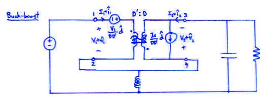
47 3.1. Derivation of DCM averaged switch model Buck-boost example Define switch terminal quantities v 1, i 1, v 2, i 2, as shown Let us find the averaged quantities v 1, i 1, v 2, i 2, for operation in DCM, and determine the relations between them v g Switch network i 1 i 2 v 1 v L L i L v 2 C R v 39
48 DCM waveforms i L i pk i 1 Area q 1 i pk 0 v L v g t v 1 v g v 0 0 v g v i 2 i pk Area q 2 Switch network i 1 i 2 v g v 1 v L L i L v 2 C R v v 2 T s v g v v 0 d 1 T s d 2 T s d 3 T s t 40
49 Basic DCM equations Peak inductor current: i 1 Area q 1 i pk Average inductor voltage: v 1 v g v v g In DCM, the diode switches off when the inductor current reaches zero. Hence, i(0) = i(t s ) = 0, and the average inductor voltage is zero. This is true even during transients. i 2 0 i pk Area q 2 v 2 v g v Solve for d 2 : T s v 0 d 1 T s d 2 T s d 3 T s t 41
50 Average switch network terminal voltages Average the v 1 waveform: i 1 Area q 1 i pk Eliminate d 2 and d 3 : v 1 v g v v g Similar analysis for v 2 waveform leads to i 2 0 i pk Area q 2 v 2 v g v T s v 0 d 1 T s d 2 T s d 3 T s t 42
51 Average switch network terminal currents Average the i 1 waveform: i 1 Area q 1 i pk The integral q 1 is the area under the i 1 waveform during first subinterval. Use triangle area formula: v 1 v g v v g 0 i 2 Eliminate i pk : i pk Area q 2 Note i 1 Ts is not equal to d i L Ts! Similar analysis for i 2 waveform leads to v 2 T s v g v v 0 d 1 T s d 2 T s d 3 T s t 43
52 Input port: Averaged equivalent circuit R e (d 1 ) Low-frequency components of input port waveforms obey Ohm s law 44
53 Output port: Averaged equivalent circuit i p v Output port is a source of power p Power p is independent of load characteristics Power p is dependent on (equal to) the power apparently consumed by the switch network input port 45
54 3.2. The dependent power source i i vi = p p v v Must avoid open- and short-circuit connections of power sources Power sink: negative p 46
55 How the power source arises in lossless two-port networks In a lossless two-port network without internal energy storage: instantaneous input power is equal to instantaneous output power In all but a small number of special cases, the instantaneous power throughput is dependent on the applied external source and load If the instantaneous power depends only on the external elements connected to one port, then the power is not dependent on the characteristics of the elements connected to the other port. The other port becomes a source of power, equal to the power flowing through the first port A power source (or power sink) element is obtained 47
56 Properties of power sources Series and parallel connection of power sources P 1 P 1 P 2 P 3 P 2 P 3 Reflection of power source through a transformer P 1 n 1 : n 2 P 1 48
57 The loss-free resistor (LFR) R e (d 1 ) A two-port lossless network Input port obeys Ohm s Law Power entering input port is transferred to output port 49
58 Averaged modeling of CCM and DCM switch networks Switch network Averaged switch model i 1 i 2 1 : d CCM v 1 v 2 i 1 i 2 DCM v 1 v 2 R e (d 1 ) 50
59 Averaged switch model: buck-boost example Original circuit Switch network i 1 i 2 v 1 v 2 v g v L L i L C R v Averaged model R e (d) C R L 51
60 3.3. Solution of averaged model: steady state Let L short circuit I 1 P C open circuit V g R e (D) R V Converter input power: Equate and solve: Converter output power: 52
61 Steady-state LFR solution is a general result, for any system that can be modeled as an LFR. For the buck-boost converter, we have Eliminate R e : which agrees with the results of previous steady-state analyses. 53
62 Steady-state LFR solution with ac terminal waveforms v g i 1 i 2 p C R R e v Converter average input power: Converter average output power: Note that no average power flows into capacitor Equate and solve: 54
63 Averaged models of other DCM converters Determine averaged terminal waveforms of switch network In each case, averaged transistor waveforms obey Ohm s law, while averaged diode waveforms behave as dependent power source Can simply replace transistor and diode with the averaged model as follows: i 1 i 2 v 1 v 2 R e (d 1 ) 55
64 DCM buck, boost Buck R e (d) L C R Boost L R e (d) C R 56
65 DCM Cuk, SEPIC Cuk L 1 C 1 L 2 R e (d) C 2 R SEPIC L 1 C 1 R e (d) L 2 C 2 R 57
66 Steady-state solution: DCM buck, boost Let L short circuit C open circuit Buck V g R e (D) P R V Boost V g R e (D) P R V 58
67 Steady-state solution of DCM/LFR models Converter M, CCM M, DCM Buck D R e /R Boost Buck-boost, Cuk SEPIC 1 1 D D 1 D D 1 D 1 1 4R/R e 2 R R e R R e 59
68
69 3.4. Small-signal ac modeling of the DCM switch network Large-signal averaged model Perturb and linearize: let R e (d) d 60
70 Linearization via Taylor series Given the nonlinear equation Expand in three-dimensional Taylor series about the quiescent operating point: (for simple notation, drop angle brackets) 61
71 Equate dc and first-order ac terms AC DC 62
72 Output port same approach DC terms Small-signal ac linearization 63
73 Output resistance parameter r 2 Power source characteristic Quiescent operating point Load characteristic Linearized model 64
74 Small-signal DCM switch model parameters Switch type g 1 j 1 r 1 g 2 j 2 r 2 Buck, Fig (a) 1 R e 2(1 M)V 1 DR e R e 2 M MR e 2(1 M)V 1 DMR e M 2 R e Boost, Fig (b) 1 2 (M 1) 2 2MV (M 1) R 1 e M D(M 1)R e R e 2M 1 (M 1) 2 R e 2V 1 D(M 1)R e (M 1) 2 R e Buck-boost, Fig. 10.7(b) 0 2V 1 DR e R e 2M R e 2V 1 DMR e M 2 R e 65
75 Small-signal ac model, DCM buck-boost example Switch network small-signal ac model C R L 66
76 A more convenient way to model the buck and boost small-signal DCM switch networks i 1 i 2 i 1 i 2 v 1 v 2 v 1 v 2 In any event, a small-signal two-port model is used, of the form 67
77 Small-signal ac models of the DCM buck and boost converters (more convenient forms) DCM buck switch network small-signal ac model L C R L DCM boost switch network small-signal ac model C R 68
78 DCM small-signal transfer functions When expressed in terms of R, L, C, and M (not D), the smallsignal transfer functions are the same in DCM as in CCM Hence, DCM boost and buck-boost converters exhibit two poles and one RHP zero in control-to-output transfer functions But, value of L is small in DCM. Hence RHP zero appears at high frequency, usually greater than switching frequency Pole due to inductor dynamics appears at high frequency, near to or greater than switching frequency So DCM buck, boost, and buck-boost converters exhibit essentially a single-pole response A simple approximation: let L 0 69
79 The simple approximation L 0 Buck, boost, and buck-boost converter models all reduce to DCM switch network small-signal ac model C R Transfer functions control-to-output with line-to-output 70
80 Transfer function salient features Converter G d0 G g0 ω p Buck 2V D 1 M 2 M M 2 M (1 M)RC Boost 2V D M 1 2M 1 M 2M 1 (M 1)RC Buck-boost V D M 2 RC 71
81 DCM boost example Control-to-output transfer function G vd (s) R = 12 Ω i L v L D 1 i D i C L = 5 µh V g Q 1 C R v C = 470 µf f s = 100 khz The output voltage is regulated to be V = 36 V. It is desired to determine G vd (s) at the operating point where the load current is I = 3 A and the dc input voltage is V g = 24 V. 72
82 Evaluate simple model parameters 73
83 Control-to-output transfer function, boost example 60 dbv G vd G vd 40 dbv G d0 37 dbv 20 dbv 0 dbv 20 dbv 40 dbv G vd 0 G vd f p 112 Hz 20 db/decade Hz 100 Hz 1 khz 10 khz 100 khz 74 f
84 4. Current programmed control of PWM converters 4.1. Averaged switch model, CCM 4.2. Ac model, CCM 4.3. DCM models 75
85 Current-programmed control Buck converter v g i s Q 1 D 1 L i L C v R The peak transistor current replaces the duty cycle as the converter control input. Measure switch current i s R f i c R f R f i s Clock Analog comparator 0 T s S Q R Latch m 1 Switch current i s Control signal i c Control input Current-programmed controller 0 dt s T s Transistor status: on off t Compensator v Clock turns transistor on Comparator turns transistor off v ref Conventional output voltage controller 76
86 A simple approximation Neglects switching ripple and artificial ramp (slope compensation) Yields physical insight and simple first-order model Accurate when converter operates well into CCM (so that switching ripple is small) and when the magnitude of the artificial ramp is not too large Well-accepted by practicing engineers Resulting small-signal relation: 77
87 4.1. Averaged switch modeling with the simple approximation Buck converter example i 1 i 2 L i L v g v 1 v 2 C R v Switch network Averaged terminal waveforms, CCM: The simple approximation: 78
88 CPM averaged switch equations Eliminate duty cycle: So: Output port is a current source Input port is a dependent current sink 79
89 CPM averaged switch model i 1 Ts i 2 Ts L i L Ts p Ts v g Ts v 1 Ts i c Ts v 2 Ts C R v Ts Averaged switch network 80
90 Results for other converters Boost i L Ts L v g Ts i c Ts p Ts C R v Ts Averaged switch network Averaged switch network Buck-boost p Ts i c Ts v g Ts C R v Ts L i L Ts 81
91 4.2. Perturbation and linearization to construct small-signal model, CCM Let Resulting input port equation: Small-signal result: Output port equation: î 2 = î c 82
92 Resulting small-signal model Buck example L C R Switch network small-signal ac model 83
93 Origin of input port negative incremental resistance i 1 Ts Power source characteristic v 1 Ts i 1 Ts = p Ts Quiescent operating point I 1 V 1 v 1 Ts 84
94 Expressing the equivalent circuit in terms of the converter input and output voltages L C R 85
95 Predicted transfer functions of the CPM buck converter L C R 86
96 Table of results basic converters r 1 r 2 C R Converter g 1 f 1 r 1 g 2 f 2 r 2 Buck D R D 1 sl R R D Boost D'R D' 1 sl D' 2 R R Buck-boost D R D 1 sl D'R D'R D 2 D2 D'R D' 1 sdl D' 2 R R D 87
97 4.3. Discontinuous conduction mode in current-programmed converters Again, use averaged switch modeling approach Result: simply replace Transistor by power sink Diode by power source Inductor dynamics appear at high frequency, near to or greater than the switching frequency Small-signal transfer functions contain a single low frequency pole DCM CPM boost and buck-boost are stable without artificial ramp DCM CPM buck without artificial ramp is stable for D < 2/3. A small artificial ramp m a 0.086m 2 leads to stability for all D. 88
98 DCM CPM buck-boost example i L i 1 Switch network i 2 v 1 v 2 i c m a i pk v g C R v L i L v L 0 t 0 89
99 Analysis i L i c m a i pk v L 0 t 0 90
100 Averaged switch input port equation i 1 Area q1 i pk i 2 i pk Area q 2 t d 1 T s d 2 T s d 3 T s T s 91
101 Discussion: switch network input port Averaged transistor waveforms obey a power sink characteristic During first subinterval, energy is transferred from input voltage source, through transistor, to inductor, equal to This energy transfer process accounts for power flow equal to which is equal to the power sink expression of the previous slide. 92
102 Averaged switch output port equation i 1 Area q1 i pk i 2 i pk Area q 2 t d 1 T s d 2 T s d 3 T s T s 93
103 Discussion: switch network output port Averaged diode waveforms obey a power sink characteristic During second subinterval, all stored energy in inductor is transferred, through diode, to load Hence, in averaged model, diode becomes a power source, having value equal to the power consumed by the transistor power sink element 94
104 Averaged equivalent circuit C R L 95
105 Steady state model: DCM CPM buck-boost V g P R V Solution for a resistive load 96
106 Models of buck and boost Buck L C R Boost L C R 97
107 Summary of steady-state DCM CPM characteristics Converter M I crit Stability range when m a = 0 Buck P load P P load 1 2 I c M m a T s 0 M < 2 3 Boost P load P load P I c M M 1 2 M m a T s 0 D 1 Buck-boost Depends on load characteristic: P load = P I c M m M 1 a T s 2 M 1 0 D 1 98
108 Buck converter: output characteristic with m a = 0 with a resistive load, there can be two operating points I I c CPM buck characteristic with m a = 0 resistive load line I = V/R the operating point having V > 0.67V g can be shown to be unstable A B CCM DCM V g V 99
109 Linearized small-signal models Buck L C R Boost L C R 100
110 Linearized small-signal models: Buck-boost C R L 101
111 DCM CPM small-signal parameters: input port Converter g 1 f 1 r 1 Buck 1 R M 2 1 M 1 m a m 1 1 m a m 1 2 I 1 I c R 1 M 1 M 2 m a m 1 1 m a m 1 Boost 1 R M M 1 2 I I c M 2 R M 2 M 2 1 m a m 1 1 m a m 1 Buck-boost 0 2 I 1 I c 1 R M 2 m a m 1 1 m a m 1 102
112 DCM CPM small-signal parameters: output port Converter g 2 f 2 r 2 Buck 1 R M 1 M m a m 1 2 M M 1 m a m 1 2 I I c R 1 M 1 m a m 1 1 2M m a m 1 Boost 1 R M M 1 2 I 2 R I M 1 c M Buck-boost 2M R m a m 1 2 I 2 I c R 1 m a m 1 103
113 Simplified DCM CPM model, with L = 0 Buck, boost, buck-boost all become C R 104
114 5. Single-phase low-harmonic rectification 5.1. The Ideal Rectifier 5.2. Integrated High-Quality Rectifier-Regulators 105
115 5.1 Properties of the Ideal Rectifier It is desired that the rectifier present a resistive load to the ac power system. This leads to unity power factor ac line current has same waveshape as voltage i ac R e is called the emulated resistance v ac R e 106
116 Control of power throughput i ac Power apparently consumed by R e is actually transferred to rectifier dc output port. To control the amount of output power, it must be possible to adjust the value of R e. v ac R e (v control ) v control 107
117 Output port model The ideal rectifier is lossless and contains no internal energy storage. Hence, the instantaneous input power equals the instantaneous output power. Since the instantaneous power is independent of the dc load characteristics, the output port obeys a power source characteristic. v ac i ac ac input Ideal rectifier (LFR) p = v 2 ac /R e R e (v control ) v control i v dc output 108
118 The dependent power source i i i vi = p p v v p v power source power sink i-v characteristic 109
119 Equations of the ideal rectifier / LFR Defining equations of the ideal rectifier: When connected to a resistive load of value R, the input and output rms voltages and currents are related as follows: A switch network that is capable of satisfying the above (averaged) equations can be employed in low-harmonic rectifier applications 110
120 Single-phase system with internal energy storage i g Ideal rectifier (LFR) i 2 p load = VI = P load v ac i ac v g R e p ac Ts C v C Dcdc converter v i load Energy storage capacitor voltage v C must be independent of input and output voltage waveforms, so that it can vary according to Energy storage capacitor This system is capable of Wide-bandwidth control of output voltage Wide-bandwidth control of input current waveform Internal independent energy storage 111
121 5.2. Integrated High-Quality Rectifier-Regulators The fact that converters can naturally exhibit the loss-free resistor characteristic suggests that one could create a single converter power stage, having a single active device, that simultaneously performs the functions of: Low-harmonic rectification / input resistor emulation Internal low-frequency energy storage Wide-bandwidth regulation of the dc output voltage High-frequency transformer isolation These properties can be achieved by: Beginning with a DCM or resonant converter that exhibits the properties of the loss-free resistor Adding a low-frequency energy storage capacitor Cascading a CCM converter, possibly having transformer isolation Integrating the cascaded converters, to share the switching element 112
122 BIBRED Boost Integrated with Buck: Rectifier / Energy storage / Dc-dc converter L 1 D 1 C 1 C 2 L2 Q 1 D 2 C 3 R v 1 : n Resembles a transformer-isolated Cuk converter, except that diode D 1 allows the input inductor to operate independently in DCM C 1 is the low-frequency energy-storage capacitor Automatic input power-factor and harmonic correction is obtained Output voltage is regulated via duty-cycle control, as in conventional dc-dc converter Variable switching frequency allows reduction of voltage variations in capacitor C 1 113
123 BIFRED Boost Integrated with Flyback: Rectifier / Energy storage / Dc-dc converter Converter power stage L 1 D 1 C 1 D 2 i 1 C 2 R v Q 1 Averaged model L 1 1 : n n : D L m (1D) : 1 R e p C 1 C 2 R Predicts converter waveforms Suitable for analytical solution or computer simulation 114 n : 1
124 Discussion Provided that the operating point variations are not too great, these converters allow reduction of the number of switches and control circuit complexity In a universal-input application in which the load power varies by a factor of 10:1 or more, the transistor voltage stress becomes too large The converter must be designed such that the input inductor operates in DCM while the output inductor operates in CCM PSPICE simulation of these circuits is not successful unless averaged models are used A number of other topologies are known 115
125 6. Three-phase low harmonic rectifiers 6.1. The ideal 3ø rectifier 6.2. Single-switch approaches to three-phase rectification 116
126 6.1. The ideal three-phase rectifier Ideal 3ø rectifier, modeled as three 1ø ideal rectifiers: 3øac input dc output ø a i a R e p a ø b i b R e p b R v ø c i c R e p c 117
127 Ideal 3ø rectifier model Combine parallel-connected power sources into a single source p tot : 3øac input dc output ø a i a R e ø b i b R e p tot = p a p b p c R v ø c i c R e 118
128 Value of p tot Ac input voltages: 3øac input ø a i a R e p a dc output ø b i b R e p b R v Instantaneous phase powers: ø c i c R e p c Total 3ø instantaneous power: 2 nd harmonic terms add to zero total 3ø power p tot is constant 119
129 Instantaneous power in ideal 3ø rectifier 3øac input dc output In a balanced system, the ideal 3ø rectifier supplies constant power to its dc output a constant power load can be supplied, without need for lowfrequency internal energy storage ø a ø b ø c i a i b i c R e R e R e p tot = p a p b p c R v 120
130 Summary The averaged switch modeling approach: replace switch network with an equivalent circuit that correctly predicts the low-frequency components of the switch network terminal waveforms PWM continuous conduction mode (CCM): switch network is modeled by a dc transformer PWM discontinuous conduction mode (DCM): transistor is replaced by effective resistor, and diode is replaced by dependent power source Current-programmed control, CCM: switch network is replaced by a current source and a dependent power sink Current-programmed control, DCM: switch network is replaced by power source and power sink Ideal rectifier: switch network is replaced by 1ø or 3ø loss-free resistor network, consisting of effective resistors and power source In each case, we can linearize to obtain the converter small-signal model. We can also easily implement these models in PSPICE 133
131
R. W. Erickson. Department of Electrical, Computer, and Energy Engineering University of Colorado, Boulder
 R. W. Erickson Department of Electrical, Computer, and Energy Engineering University of Colorado, Boulder 18.2.2 DCM flyback converter v ac i ac EMI filter i g v g Flyback converter n : 1 L D 1 i v C R
R. W. Erickson. Department of Electrical, Computer, and Energy Engineering University of Colorado, Boulder
 R. W. Erickson Department of Electrical, Computer, and Energy Engineering University of Colorado, Boulder 17.1 The single-phase full-wave rectifier i g i L L D 4 D 1 v g Z i C v R D 3 D 2 Full-wave rectifier
R. W. Erickson. Department of Electrical, Computer, and Energy Engineering University of Colorado, Boulder
 R. W. Erickson Department of Electrical, Computer, and Energy Engineering University of Colorado, Boulder 6.3.5. Boost-derived isolated converters A wide variety of boost-derived isolated dc-dc converters
R. W. Erickson. Department of Electrical, Computer, and Energy Engineering University of Colorado, Boulder
 R. W. Erickson Department of Electrical, Computer, and Energy Engineering University of Colorado, Boulder B.3 Simulation of Current Mode Controllers Develop a model of the currentprogrammed controller,
Chapter 6: Converter circuits
 Chapter 6. Converter Circuits 6.1. Circuit manipulations 6.2. A short list of converters 6.3. Transformer isolation 6.4. Converter evaluation and design 6.5. Summary of key points Where do the boost, buck-boost,
R. W. Erickson. Department of Electrical, Computer, and Energy Engineering University of Colorado, Boulder
 R. W. Erickson Department of Electrical, Computer, and Energy Engineering University of Colorado, Boulder 18.5 RMS values of rectifier waveforms Doubly-modulated transistor current waveform, boost rectifier:
Power Management for Computer Systems. Prof. C Wang
 ECE 5990 Power Management for Computer Systems Prof. C Wang Fall 2010 Course Outline Fundamental of Power Electronics cs for Computer Systems, Handheld Devices, Laptops, etc More emphasis in DC DC converter
Fundamentals of Power Electronics
 Fundamentals of Power Electronics SECOND EDITION Robert W. Erickson Dragan Maksimovic University of Colorado Boulder, Colorado Preface 1 Introduction 1 1.1 Introduction to Power Processing 1 1.2 Several
OWING TO THE growing concern regarding harmonic
 IEEE TRANSACTIONS ON INDUSTRIAL ELECTRONICS, VOL. 46, NO. 4, AUGUST 1999 749 Integrated High-Quality Rectifier Regulators Michael T. Madigan, Member, IEEE, Robert W. Erickson, Senior Member, IEEE, and
Lecture 4 ECEN 4517/5517
 Lecture 4 ECEN 4517/5517 Experiment 3 weeks 2 and 3: interleaved flyback and feedback loop Battery 12 VDC HVDC: 120-200 VDC DC-DC converter Isolated flyback DC-AC inverter H-bridge v ac AC load 120 Vrms
Lecture 8 ECEN 4517/5517
 Lecture 8 ECEN 4517/5517 Experiment 4 Lecture 7: Step-up dcdc converter and PWM chip Lecture 8: Design of analog feedback loop Part I Controller IC: Demonstrate operating PWM controller IC (UC 3525) Part
Final Exam. Anyone caught copying or allowing someone to copy from them will be ejected from the exam.
 Final Exam EECE 493-101 December 4, 2008 Instructor: Nathan Ozog Name: Student Number: Read all of the following information before starting the exam: The duration of this exam is 3 hours. Anyone caught
R. W. Erickson. Department of Electrical, Computer, and Energy Engineering University of Colorado, Boulder
 R. W. Erickson Department of Electrical, Computer, and Energy Engineering University of Colorado, Boulder Construction of transfer function v 2 (s) v (s) = Z 2Z Z Z 2 Z = Z out Z R C Z = L Q = R /R 0 f
Chapter 1: Introduction
 1.1. Introduction to power processing 1.2. Some applications of power electronics 1.3. Elements of power electronics Summary of the course 2 1.1 Introduction to Power Processing Power input Switching converter
S. General Topological Properties of Switching Structures, IEEE Power Electronics Specialists Conference, 1979 Record, pp , June 1979.
 Problems 179 [22] [23] [24] [25] [26] [27] [28] [29] [30] J. N. PARK and T. R. ZALOUM, A Dual Mode Forward/Flyback Converter, IEEE Power Electronics Specialists Conference, 1982 Record, pp. 3-13, June
R. W. Erickson. Department of Electrical, Computer, and Energy Engineering University of Colorado, Boulder
 R. W. Erickson Department of Electrical, Computer, and Energy Engineering University of Colorado, Boulder Inclusion of Switching Loss in the Averaged Equivalent Circuit Model The methods of Chapter 3 can
Resonant Power Conversion
 Resonant Power Conversion Prof. Bob Erickson Colorado Power Electronics Center Department of Electrical, Computer, and Energy Engineering University of Colorado, Boulder Outline. Introduction to resonant
SIMULATION WITH THE CUK TOPOLOGY ECE562: Power Electronics I COLORADO STATE UNIVERSITY. Modified in Fall 2011
 SIMULATION WITH THE CUK TOPOLOGY ECE562: Power Electronics I COLORADO STATE UNIVERSITY Modified in Fall 2011 ECE 562 Cuk Converter (NL5 Simulation) Laboratory Page 1 PURPOSE: The purpose of this lab is
A New Quadratic Boost Converter with PFC Applications
 Proceedings of the th WSEAS International Conference on CICUITS, uliagmeni, Athens, Greece, July -, 6 (pp3-8) A New Quadratic Boost Converter with PFC Applications DAN LASCU, MIHAELA LASCU, IOAN LIE, MIHAIL
R. W. Erickson. Department of Electrical, Computer, and Energy Engineering University of Colorado, Boulder
 R. W. Erickson Department of Electrical, Computer, and Energy Engineering University of Colorado, Boulder pn junction! Junction diode consisting of! p-doped silicon! n-doped silicon! A p-n junction where
Lecture 6 ECEN 4517/5517
 Lecture 6 ECEN 4517/5517 Experiment 4: inverter system Battery 12 VDC HVDC: 120-200 VDC DC-DC converter Isolated flyback DC-AC inverter H-bridge v ac AC load 120 Vrms 60 Hz d d Feedback controller V ref
LECTURE 40 Introduction to Converter Dynamics A. AC Model Construction 1. Actual Switch mode Non-Linear System 2. Small AC Models by two Analytical
 LECTURE 40 Introduction to Converter Dynamics A. AC Model Construction 1. Actual Switch mode Non-Linear System 2. Small AC Models by two Analytical Paths a. Circuit averaging over T s b. State space Averaging
ADVANCES IN AVERAGED SWITCH MODELING
 ADVANES IN AVEAGED SWITH MODEING obert W. Erickson Power Electronics Group Department of Electrical and omputer Engineering University of olorado Boulder, O USA 80309-0425 rwe@boulder.colorado.edu http://ece-www.colorado.edu/~pwrelect
DESIGN AND ANALYSIS OF FEEDBACK CONTROLLERS FOR A DC BUCK-BOOST CONVERTER
 DESIGN AND ANALYSIS OF FEEDBACK CONTROLLERS FOR A DC BUCK-BOOST CONVERTER Murdoch University: The Murdoch School of Engineering & Information Technology Author: Jason Chan Supervisors: Martina Calais &
Chapter 3 : Closed Loop Current Mode DC\DC Boost Converter
 Chapter 3 : Closed Loop Current Mode DC\DC Boost Converter 3.1 Introduction DC/DC Converter efficiently converts unregulated DC voltage to a regulated DC voltage with better efficiency and high power density.
VOLTAGE MODE CONTROL OF SOFT SWITCHED BOOST CONVERTER BY TYPE II & TYPE III COMPENSATOR
 1002 VOLTAGE MODE CONTROL OF SOFT SWITCHED BOOST CONVERTER BY TYPE II & TYPE III COMPENSATOR NIKITA SINGH 1 ELECTRONICS DESIGN AND TECHNOLOGY, M.TECH NATIONAL INSTITUTE OF ELECTRONICS AND INFORMATION TECHNOLOGY
ECEN 5807 Modeling and Control of Power Electronic Systems
 ECEN 5807 Modeling and Control of Power Electronic Systems Instructor: Prof. Bob Erickson Office telephone: (303) 492-7003 Fax: (303) 492-2758 Email: rwe@colorado.edu Course web page http://ece.colorado.edu/~ecen5807
Elements of Power Electronics PART II: Topologies and applications
 Elements of Power Electronics PART II: Topologies and applications Fabrice Frébel (fabrice.frebel@ulg.ac.be) September 2 st, 207 PART II: Topologies and applications Chapter 6: Converter Circuits Applications
EEL 646 POWER ELECTRONICS II. Issa Batarseh. January 13, 2015
 EEL 646 POWER ELECTRONICS II Issa Batarseh January 13, 2015 Agenda About the course Syllabus Review Course Topics Review of Power Electronics I Questions Introduction (cont d) Introduction (cont d) 5
ECEN4797/5797 Lecture #11
 ECEN4797/5797 Lecture #11 Announcements On-campus students: pick up graded HW2, turn in HW3 Homework 4 is due in class on Friday, Sept. 23. The grace-period for offcampus students expires 5pm (Mountain)
IMPLEMENTATION OF A DOUBLE AC/DC/AC CONVERTER WITH POWER FACTOR CORRECTION (PFC) FOR NON-LINEAR LOAD APPLICATIONS
 FOR NON-LINEAR LOAD APPLICATIONS") IMPLEMENTATION OF A DOUBLE AC/DC/AC CONERTER WITH POWER FACTOR CORRECTION (PFC) FOR NON-LINEAR LOAD APPLICATIONS E.Alvear 1, M.Sanchez 1 and J.Posada 2 1 Department of Automation and Electronics, Electronics
IMPLEMENTATION OF A DOUBLE AC/DC/AC CONERTER WITH POWER FACTOR CORRECTION (PFC) FOR NON-LINEAR LOAD APPLICATIONS E.Alvear 1, M.Sanchez 1 and J.Posada 2 1 Department of Automation and Electronics, Electronics
Lecture 41 SIMPLE AVERAGING OVER T SW to ACHIEVE LOW FREQUENCY MODELS
 Lecture 41 SIMPLE AVERAGING OVER T SW to ACHIEVE LOW FREQUENCY MODELS. Goals and Methodology to Get There 0. Goals 0. Methodology. BuckBoost and Other Converter Models 0. Overview of Methodology 0. Example
Linear Peak Current Mode Controlled Non-inverting Buck-Boost Power-Factor-Correction Converter
 Linear Peak Current Mode Controlled Non-inverting Buck-Boost Power-Factor-Correction Converter Mr.S.Naganjaneyulu M-Tech Student Scholar Department of Electrical & Electronics Engineering, VRS&YRN College
R. W. Erickson. Department of Electrical, Computer, and Energy Engineering University of Colorado, Boulder
 R. W. Erickson Department o Electrical, Computer, and Energy Engineering University o Colorado, Boulder Computation ohase! T 60 db 40 db 20 db 0 db 20 db 40 db T T 1 Crossover requency c 1 Hz 10 Hz 100
A Novel Control Method to Minimize Distortion in AC Inverters. Dennis Gyma
 A Novel Control Method to Minimize Distortion in AC Inverters Dennis Gyma Hewlett-Packard Company 150 Green Pond Road Rockaway, NJ 07866 ABSTRACT In PWM AC inverters, the duty-cycle modulator transfer
Power supplies are one of the last holdouts of true. The Purpose of Loop Gain DESIGNER SERIES
 DESIGNER SERIES Power supplies are one of the last holdouts of true analog feedback in electronics. For various reasons, including cost, noise, protection, and speed, they have remained this way in the
Small signal modeling and steady state stability analysis of PWM based switch model Boost converter using Pspise
 Small signal modeling and steady state stability analysis of PWM based switch model Boost converter using Pspise Mrs. Swapna Manurkar Assistant Professor, Electrical Engineering, Vishwaniketan s Institute
Research and design of PFC control based on DSP
 Acta Technica 61, No. 4B/2016, 153 164 c 2017 Institute of Thermomechanics CAS, v.v.i. Research and design of PFC control based on DSP Ma Yuli 1, Ma Yushan 1 Abstract. A realization scheme of single-phase
EE 486 Power Electronics Final Exam Coverage Prof. Ali Mehrizi-Sani
 EE 486 Power Electronics Final Exam Coverage Prof. Ali Mehrizi-Sani mehrizi@eecs.wsu.edu School of Electrical Engineering and Computer Science April 26, 2012 Illusions 2 of 18 Final Exam Coverage All Material
A New Averaged Switch Model Including Conduction Losses for PWM Converters Operating in Discontinuous Inductor Current Mode
 FACTA UNIVERSITATIS (NIŠ) SER.: ELEC. ENERG. vol. 19, no. 2, August 2006, 219-230 A New Averaged Switch Model Including Conduction Losses for PWM Converters Operating in Discontinuous Inductor Current
DC DC POWER CONVERTERS CHOPPERS SWITCHING POWER SUPPLIES INTRODUCTION
 DC DC POWER CONVERTERS CHOPPERS SWITCHING POWER SUPPLIES INTRODUCTION Direct current direct current (dc dc) power converters are employed in a variety of applications, including power supplies for personal
Fig.1. A Block Diagram of dc-dc Converter System
 ANALYSIS AND SIMULATION OF BUCK SWITCH MODE DC TO DC POWER REGULATOR G. C. Diyoke Department of Electrical and Electronics Engineering Michael Okpara University of Agriculture, Umudike Umuahia, Abia State
Constant-Frequency Soft-Switching Converters. Soft-switching converters with constant switching frequency
 Constant-Frequency Soft-Switching Converters Introduction and a brief survey Active-clamp (auxiliary-switch) soft-switching converters, Active-clamp forward converter Textbook 20.4.2 and on-line notes
Bridgeless Cuk Power Factor Corrector with Regulated Output Voltage
 Bridgeless Cuk Power Factor Corrector with Regulated Output Voltage Ajeesh P R 1, Prof. Dinto Mathew 2, Prof. Sera Mathew 3 1 PG Scholar, 2,3 Professors, Department of Electrical and Electronics Engineering,
R. W. Erickson. Department of Electrical, Computer, and Energy Engineering University of Colorado, Boulder
 R. W. Erickson Department of Electrical, Computer, and Energy Engineering University of Colorado, Boulder 16.4. Power phasors in sinusoidal systems Apparent power is the product of the rms voltage and
Modeling of switched DC-DC converters by mixed s-z description
 Modeling of switched C-C converters by mixed s-z description alibor Biolek, Viera Biolková*) Inst. of Microelectronics (Radioelectronics*) FEEC BU, Brno, Czech Republic fax: 97344987 - e-mail: dalibor.biolek@unob.cz
3.1 ignored. (a) (b) (c)
 (b) (c)") Problems 57 [2] [3] [4] S. Modeling, Analysis, and Design of Switching Converters, Ph.D. thesis, California Institute of Technology, November 1976. G. WESTER and R. D. MIDDLEBROOK, Low-Frequency Characterization
Problems 57 [2] [3] [4] S. Modeling, Analysis, and Design of Switching Converters, Ph.D. thesis, California Institute of Technology, November 1976. G. WESTER and R. D. MIDDLEBROOK, Low-Frequency Characterization
Chapter 2 Buck PWM DC DC Converter
 Chapter 2 Buck PWM DC DC Converter H. Wang, Power Management and High-speed I/O in CMOS Systems 1/25 Buck Circuit and Its equivalent circuits CCM: continuous conduction mode DCM: discontinuous conduction
BUCK Converter Control Cookbook
 BUCK Converter Control Cookbook Zach Zhang, Alpha & Omega Semiconductor, Inc. A Buck converter consists of the power stage and feedback control circuit. The power stage includes power switch and output
Single Phase Bridgeless SEPIC Converter with High Power Factor
 International Journal of Emerging Engineering Research and Technology Volume 2, Issue 6, September 2014, PP 117-126 ISSN 2349-4395 (Print) & ISSN 2349-4409 (Online) Single Phase Bridgeless SEPIC Converter
Impact of inductor current ringing in DCM on output voltage of DC-DC buck power converters
 ARCHIVES OF ELECTRICAL ENGINEERING VOL. 66(2), pp. 313-323 (2017) DOI 10.1515/aee-2017-0023 Impact of inductor current ringing in DCM on output voltage of DC-DC buck power converters MARCIN WALCZAK Department
The Effect of Ripple Steering on Control Loop Stability for a CCM PFC Boost Converter
 The Effect of Ripple Steering on Control Loop Stability for a CCM PFC Boost Converter Fariborz Musavi, Murray Edington Department of Research, Engineering Delta-Q Technologies Corp. Burnaby, BC, Canada
Design and Simulation of New Efficient Bridgeless AC- DC CUK Rectifier for PFC Application
 Design and Simulation of New Efficient Bridgeless AC- DC CUK Rectifier for PFC Application Thomas Mathew.T PG Student, St. Joseph s College of Engineering, C.Naresh, M.E.(P.hd) Associate Professor, St.
Digital Simulation and Analysis of Sliding Mode Controller for DC-DC Converter using Simulink
 Volume-7, Issue-3, May-June 2017 International Journal of Engineering and Management Research Page Number: 367-371 Digital Simulation and Analysis of Sliding Mode Controller for DC-DC Converter using Simulink
is demonstrated by considering the conduction resistances and their voltage drop in DCM. This paper presents DC and small-signal circuit models of the
 Average Model of Boost Converter, including Parasitics, operating in Discontinuous Conduction Mode (DCM) Haytham Abdelgawad and Vijay Sood Faculty of Engineering and Applied Science, University of Ontario
CHAPTER 3 MAXIMUM POWER TRANSFER THEOREM BASED MPPT FOR STANDALONE PV SYSTEM
 60 CHAPTER 3 MAXIMUM POWER TRANSFER THEOREM BASED MPPT FOR STANDALONE PV SYSTEM 3.1 INTRODUCTION Literature reports voluminous research to improve the PV power system efficiency through material development,
IT is well known that the boost converter topology is highly
 320 IEEE TRANSACTIONS ON POWER ELECTRONICS, VOL. 21, NO. 2, MARCH 2006 Analysis and Design of a Low-Stress Buck-Boost Converter in Universal-Input PFC Applications Jingquan Chen, Member, IEEE, Dragan Maksimović,
Lecture 7: MOSFET, IGBT, and Switching Loss
 Lecture 7: MOSFET, IGBT, and Switching Loss ECE 481: Power Electronics Prof. Daniel Costinett Department of Electrical Engineering and Computer Science University of Tennessee Knoxville Fall 2013 Announcements
SIMULATION WITH THE BOOST TOPOLOGY ECE562: Power Electronics I COLORADO STATE UNIVERSITY. Modified in Fall 2011
 SIMULATION WITH THE BOOST TOPOLOGY ECE562: Power Electronics I COLORADO STATE UNIVERSITY Modified in Fall 2011 ECE 562 Boost Converter (NL5 Simulation) Laboratory 2 Page 1 PURPOSE: The purpose of this
TSTE25 Power Electronics. Lecture 6 Tomas Jonsson ISY/EKS
 TSTE25 Power Electronics Lecture 6 Tomas Jonsson ISY/EKS 2016-11-15 2 Outline DC power supplies DC-DC Converter Step-down (buck) Step-up (boost) Other converter topologies (overview) Exercises 7-1, 7-2,
A New 3-phase Buck-Boost Unity Power Factor Rectifier with Two Independently Controlled DC Outputs
 A New 3-phase Buck-Boost Unity Power Factor Rectifier with Two Independently Controlled DC Outputs Y. Nishida* 1, J. Miniboeck* 2, S. D. Round* 2 and J. W. Kolar* 2 * 1 Nihon University Energy Electronics
CHAPTER 3. SINGLE-STAGE PFC TOPOLOGY GENERALIZATION AND VARIATIONS
 CHAPTER 3. SINGLE-STAGE PFC TOPOLOG GENERALIATION AND VARIATIONS 3.1. INTRODUCTION The original DCM S 2 PFC topology offers a simple integration of the DCM boost rectifier and the PWM DC/DC converter.
CHAPTER 3 APPLICATION OF THE CIRCUIT MODEL FOR PHOTOVOLTAIC ENERGY CONVERSION SYSTEM
 63 CHAPTER 3 APPLICATION OF THE CIRCUIT MODEL FOR PHOTOVOLTAIC ENERGY CONVERSION SYSTEM 3.1 INTRODUCTION The power output of the PV module varies with the irradiation and the temperature and the output
A New Small-Signal Model for Current-Mode Control Raymond B. Ridley
 A New Small-Signal Model for Current-Mode Control Raymond B. Ridley Copyright 1999 Ridley Engineering, Inc. A New Small-Signal Model for Current-Mode Control By Raymond B. Ridley Before this book was written
MICROCONTROLLER BASED BOOST PID MUNAJAH BINTI MOHD RUBAEE
 MICROCONTROLLER BASED BOOST PID MUNAJAH BINTI MOHD RUBAEE This thesis is submitted as partial fulfillment of the requirement for the award of Bachelor of Electrical Engineering (Power System) Faculty of
55:141 Advanced Circuit Techniques Switching Regulators
 55:141 Advanced Circuit Techniques Switching Regulators Material: ecture Notes, Handouts, and Sections of Chapter 11 of Franco A. Kruger 55:141: Advanced Circuit Techniques The University of Iowa Switching
CHAPTER 2 GENERAL STUDY OF INTEGRATED SINGLE-STAGE POWER FACTOR CORRECTION CONVERTERS
 CHAPTER 2 GENERAL STUDY OF INTEGRATED SINGLE-STAGE POWER FACTOR CORRECTION CONVERTERS 2.1 Introduction Conventional diode rectifiers have rich input harmonic current and cannot meet the IEC PFC regulation,
55:141 Advanced Circuit Techniques Switching Regulators
 55:141 Advanced Circuit Techniques Switching Regulators Material: ecture Notes, Handouts, and Sections of Chapter 11 of Franco A. Kruger 55:141: Advanced Circuit Techniques The University of Iowa Switching
3. Discrete and Continuous-Time Analysis of Current-Mode Cell
 3. Discrete and Continuous-Time Analysis of Current-Mode Cell 3.1 ntroduction Fig. 3.1 shows schematics of the basic two-state PWM converters operating with current-mode control. The sensed current waveform
Modified SEPIC PFC Converter for Improved Power Factor and Low Harmonic Distortion
 Modified SEPIC PFC Converter for Improved Power Factor and Low Harmonic Distortion Amrutha M P 1, Priya G Das 2 1, 2 Department of EEE, Abdul Kalam Technological University, Palakkad, Kerala, India-678008
Neuro Fuzzy Control Single Stage Single Phase AC-DC Converter for High Power factor
 Neuro Fuzzy Control Single Stage Single Phase AC-DC Converter for High Power factor S. Lakshmi Devi M.Tech(PE),Department of EEE, Prakasam Engineering College,Kandukur,A.P K. Sudheer Assoc. Professor,
CHAPTER 5 The Parallel Resonant Converter
 CHAPTER 5 The Parallel Resonant Converter T he objective of this chapter is to describe the operation of the parallel resonant converter in detail. The concepts developed in chapter 3 are used to derive
CHAPTER 5 DESIGN OF SINUSOIDAL PULSE WIDTH MODULATION TECHNIQUES FOR ZETA CONVERTER USING FPGA
 82 CHAPTER 5 DESIGN OF SINUSOIDAL PULSE WIDTH MODULATION TECHNIQUES FOR ZETA CONVERTER USING FPGA 5.1 Introduction Similar to the SEPIC DC/DC converter topology, the ZETA converter topology provides a
Circuit Simulation. LTSpice Modeling Examples
 Power Stage Losses Conduction Losses MOSFETS IGBTs Diodes Inductor Capacitors R on r ce V F R dc ESR V ce R d Frequency Dependent Losses C oss Current C d tailing Reverse Recovery Skin Effect Core Loss
ECE514 Power Electronics Converter Topologies. Part 2 [100 pts] Design of an RDC snubber for flyback converter
![ECE514 Power Electronics Converter Topologies. Part 2 [100 pts] Design of an RDC snubber for flyback converter](/thumbs/72/67440195.jpg "ECE514 Power Electronics Converter Topologies. Part 2 [100 pts] Design of an RDC snubber for flyback converter") ECE514 Power Electronics Converter Topologies Homework Assignment #4 Due date October 31, 2014, beginning of the lecture Part 1 [100 pts] Redo Term Test 1 (attached) Part 2 [100 pts] Design of an RDC snubber
ECE514 Power Electronics Converter Topologies Homework Assignment #4 Due date October 31, 2014, beginning of the lecture Part 1 [100 pts] Redo Term Test 1 (attached) Part 2 [100 pts] Design of an RDC snubber
CHAPTER 2 DESIGN AND MODELING OF POSITIVE BUCK BOOST CONVERTER WITH CASCADED BUCK BOOST CONVERTER
 17 CHAPTER 2 DESIGN AND MODELING OF POSITIVE BUCK BOOST CONVERTER WITH CASCADED BUCK BOOST CONVERTER 2.1 GENERAL Designing an efficient DC to DC buck-boost converter is very much important for many real-time
Chapter 2 MODELING AND CONTROL OF PEBB BASED SYSTEMS
 Chapter 2 MODELING AND CONTROL OF PEBB BASED SYSTEMS 2.1 Introduction The PEBBs are fundamental building cells, integrating state-of-the-art techniques for large scale power electronics systems. Conventional
ACONTROL technique suitable for dc dc converters must
 96 IEEE TRANSACTIONS ON POWER ELECTRONICS, VOL. 12, NO. 1, JANUARY 1997 Small-Signal Analysis of DC DC Converters with Sliding Mode Control Paolo Mattavelli, Member, IEEE, Leopoldo Rossetto, Member, IEEE,
Input output linearization with non-minimum phase boost DC-DC converters
 NOLTA, IEICE Paper Input output linearization with non-minimum phase boost DC-DC converters Vikas Paduvalli 1a), Robert Taylor 2,LouisHunt 1, and Poras T Balsara 1 1 Electrical Engineering, The University
6.334 Final Project Buck Converter
 Nathan Monroe monroe@mit.edu 4/6/13 6.334 Final Project Buck Converter Design Input Filter Filter Capacitor - 40µF x 0µF Capstick CS6 film capacitors in parallel Filter Inductor - 10.08µH RM10/I-3F3-A630
CHAPTER 1 DIODE CIRCUITS. Semiconductor act differently to DC and AC currents
 CHAPTER 1 DIODE CIRCUITS Resistance levels Semiconductor act differently to DC and AC currents There are three types of resistances 1. DC or static resistance The application of DC voltage to a circuit
METHODS TO IMPROVE DYNAMIC RESPONSE OF POWER FACTOR PREREGULATORS: AN OVERVIEW
 METHODS TO IMPROE DYNAMIC RESPONSE OF POWER FACTOR PREREGULATORS: AN OERIEW G. Spiazzi*, P. Mattavelli**, L. Rossetto** *Dept. of Electronics and Informatics, **Dept. of Electrical Engineering University
4.5V to 32V Input High Current LED Driver IC For Buck or Buck-Boost Topology CN5816. Features: SHDN COMP OVP CSP CSN
 4.5V to 32V Input High Current LED Driver IC For Buck or Buck-Boost Topology CN5816 General Description: The CN5816 is a current mode fixed-frequency PWM controller for high current LED applications. The
A Control Scheme for an AC-DC Single-Stage Buck-Boost PFC Converter with Improved Output Ripple Reduction
 Western University Scholarship@Western Electronic Thesis and Dissertation Repository August 2012 A Control Scheme for an AC-DC Single-Stage Buck-Boost PFC Converter with Improved Output Ripple Reduction
A HIGH RELIABILITY SINGLE-PHASE BOOST RECTIFIER SYSTEM FOR DIFFERENT LOAD VARIATIONS. Prasanna Srikanth Polisetty
 GRT A HIGH RELIABILITY SINGLE-PHASE BOOST RECTIFIER SYSTEM FOR DIFFERENT LOAD VARIATIONS Prasanna Srikanth Polisetty Department of Electrical and Electronics Engineering, Newton s College of Engineering
CHAPTER 3 CUK CONVERTER BASED MPPT SYSTEM USING ADAPTIVE PAO ALGORITHM
 52 CHAPTER 3 CUK CONVERTER BASED MPPT SYSTEM USING ADAPTIVE PAO ALGORITHM 3.1 INTRODUCTION The power electronics interface, connected between a solar panel and a load or battery bus, is a pulse width modulated
CHAPTER IV DESIGN AND ANALYSIS OF VARIOUS PWM TECHNIQUES FOR BUCK BOOST CONVERTER
 59 CHAPTER IV DESIGN AND ANALYSIS OF VARIOUS PWM TECHNIQUES FOR BUCK BOOST CONVERTER 4.1 Conventional Method A buck-boost converter circuit is a combination of the buck converter topology and a boost converter
Digital Control Techniques for Single-Phase Power Factor Correction Rectifiers
 University of Colorado, Boulder CU Scholar Electrical, Computer & Energy Engineering Graduate Theses & Dissertations Electrical, Computer & Energy Engineering Spring 1-1-2010 Digital Control Techniques
2.4 Modeling and Analysis of Three Phase Four Leg Inverter
 2.4 Modeling and Analysis of Three Phase Four Leg Inverter The main feature of a three phase inverter, with an additional neutral leg, is its ability to deal with load unbalance in a standalone power supply
AN2388. Peak Current Controlled ZVS Full-Bridge Converter with Digital Slope Compensation ABSTRACT INTRODUCTION
 Peak Current Controlled ZVS Full-Bridge Converter with Digital Slope Compensation Author: ABSTRACT This application note features a detailed discussion on plant modeling, control system design and firmware
Reduction of Voltage Stresses in Buck-Boost-Type Power Factor Correctors Operating in Boundary Conduction Mode
 Reduction of oltage Stresses in Buck-Boost-Type Power Factor Correctors Operating in Boundary Conduction Mode ars Petersen Institute of Electric Power Engineering Technical University of Denmark Building
11. Define the term pinch off voltage of MOSFET. (May/June 2012)
") Subject Code : EE6503 Branch : EEE Subject Name : Power Electronics Year/Sem. : III /V Unit - I PART-A 1. State the advantages of IGBT over MOSFET. (Nov/Dec 2008) 2. What is the function of snubber circuit?
Subject Code : EE6503 Branch : EEE Subject Name : Power Electronics Year/Sem. : III /V Unit - I PART-A 1. State the advantages of IGBT over MOSFET. (Nov/Dec 2008) 2. What is the function of snubber circuit?
Digital PWM Controller and Current Estimator for A Low-Power Switching Converter
 7 th IEEE Workshop on Computers in Power Electronics, COMPE 000, Blacksburg, VA, July 6-8, 000. Digital PWM Controller and Current Estimator for A ow-power Switching Converter Aleksandar Prodic and Dragan
ELEC387 Power electronics
 ELEC387 Power electronics Jonathan Goldwasser 1 Power electronics systems pp.3 15 Main task: process and control flow of electric energy by supplying voltage and current in a form that is optimally suited
Non-linear Control. Part III. Chapter 8
 Chapter 8 237 Part III Chapter 8 Non-linear Control The control methods investigated so far have all been based on linear feedback control. Recently, non-linear control techniques related to One Cycle
Half bridge converter. DC balance with current signal injection
 Runo Nielsen page of 569 Tommerup telephone : +45 64 76 email : runo.nielsen@tdcadsl.dk December Control methods in pulse width modulated converters The half bridge converter has been around for many years.
Oscillators. An oscillator may be described as a source of alternating voltage. It is different than amplifier.
 Oscillators An oscillator may be described as a source of alternating voltage. It is different than amplifier. An amplifier delivers an output signal whose waveform corresponds to the input signal but
Chapter 6. Small signal analysis and control design of LLC converter
 Chapter 6 Small signal analysis and control design of LLC converter 6.1 Introduction In previous chapters, the characteristic, design and advantages of LLC resonant converter were discussed. As demonstrated
Digital Control Techniques for Efficiency Improvements in Single-Phase Boost Power Factor Correction Rectifiers
 University of Colorado, Boulder CU Scholar Electrical, Computer & Energy Engineering Graduate Theses & Dissertations Electrical, Computer & Energy Engineering Spring 1-1-2010 Digital Control Techniques
Modeling and Simulation of Power Electronic Converters
 Modeling and Simulation of Power Electronic Converters DRAGAN MAKSIMOVIĆ, MEMBER, IEEE, ALEKSANDAR M. STANKOVIĆ, MEMBER, IEEE, V. JOSEPH THOTTUVELIL, MEMBER, IEEE, AND GEORGE C. VERGHESE, FELLOW, IEEE