CY520 Datasheet. 300M-450MHz ASK Receiver. General Description. Features. Applications CY520
|
|
|
- Allan Holmes
- 5 years ago
- Views:
Transcription

1 CY520 Datasheet 300M-450MHz ASK Receiver General Description The CY520 is a general purpose, 3.3-5V ASK Receiver that operates from 300M to 450MHz with typical sensitivity of -109dBm. The CY520 functions as a super-heterodyne receiver for OOK and ASK modulation up to 10kbps. The down-conversion mixer also provides image rejection. All post-detection data filtering is provided on the CY520. Any one-of-four filter bandwidths may be selected externally by the user in binary steps, from 1.25 khz to 10kHz. The user need only configure the device with a set of easily determined values, based upon data rate, code modulation format, and desired duty-cycle operation. CY520 is the SOP8 package version Features -109dBm sensitivity, 1kbps and BER 10E-02 Frequency from 300MHz to 450MHz Supply Voltage form 3V to 5.5V Image Rejection Mixer Data-rate up to 10kbps(fixed-mode) Low power, 6.0mA, 3.9mA, continuous on data rates to 10kbps(Manchester Encoded) No IF filter required Excellent selectivity and noise rejection Analog RSSI Output Applications Automotive Remote Keyless Entry (RKE) Remote Controls Remote fan and light control Garage door and gate openers Page 1 of 17
2 Typical Application MHz 1K Baud Rate Example Pin Configuration CY520 SOP8 Pin Description Pin Name RO1 ANT VDD VSS RO2 CAGC Pin Function Reference resonator input connection o Colpitts oscillator stage. May also be driven by external reference signal of 1.5V p-p amplitude maximum. RF signal input from antenna. Internally AC coupled. It is recommended that a matching network with an inductor-to-rf ground is used to improve ESD protection. Positive supply connection for all chip functions. Negative supply connection for all chip functions except RF input. Reference resonator input connection to Colpitts oscillator stage, a 18pF capacitor is connected from this pin to GND during normal operation. AGC filter capacitor connection. CAGC capacitor, normally greater than 0.47μF, is connected from this pin to GND. Page 2 of 17
3 CTH DO Demodulation threshold voltage integration capacitor connection. Tie an external capacitor across CTH pin and GND to set the setting time for the demodulation data slicing level. Values about 1nF are recommended and should be optimized for data rate and data profile. Demodulated data output Absolute Maximum Ratings (1) Supply Voltage(V DD ) +7V Input Voltage +7V Junction Temperature(T J ) +150 Storage Temperature Range(T S ) -65 to +150 Lead Temperature (soldering, 10sec.) +260 Maximum Receiver Input Power +10dBm ESD Rating Note 3 Operating Ratings (2) RF Frequency Range 300MHz to 450MHz Supply Voltage(VDD) +3.0V to +5.5V Input Voltage(VIN) 5.5V (Max.) Maximum Input RF Power -20dBm Ambient Temperature(TA) -30 to +85 Electrical Characteristics (4) Specifications apply for 3.0V < V DD < 3.6V, V SS = 0V, C AGC = 4.7μF, C TH = 0.1μF, f RX = MHz, unless otherwise noted. Bold values indicate 20 C T A 70 C. 1kbps data rate (Manchester encoded), reference oscillator frequency = MHz. Symbol Parameter Condition Min. Typ. Max. Units V DD =3.3V, F RX =433.92MHz 6.0 ma I SS Operating Supply V DD =5V, F RX =433.92MHz 7.0 ma Current V DD =3.3V, F RX =315MHz 3.9 ma V DD =5V, F RX =315MHz 4.7 ma I SHUT Shut Down Current 0.5 μa Page 3 of 17
4 RF Section, IF Section Symbol Parameter Condition Min Typ. Max Units Image Rejection 20 db 1*IF Center f RX =433.92MHz 1.2 MHz Frequency f RX =315MHz 0.86 MHz Receiver f RX =433.92MHz, V DD =5V(matched to 50Ω) BER= dbm f RX =315MHz, V DD =5V(matched to 50Ω) BER= dbm IF Bandwidth f RX =433.92MHz 330 khz f RX =315MHz 235 khz 19- f RX =433.92MHz Ω j174 Antenna Input 32.5 Impedance f RX =315MHz - Ω J235 Receive Modulation Duty Cycle Note % AGC Attack/ Decay Ratio t ATTACK /t DECAY 0.1 AGC pin leakage T A =25 ±2 na current T A =105 ±800 na AGC Dynamic RF 1.15 V Range RF 1.70 V Reference Oscillator Symbol Parameter Condition Min. Typ. Max. Units f RX =433.92MHz Reference Oscillator Crystal Load Cap=10pF 7 MHz Frequency f RX =315MHz Crystal Load Cap=10pF MHz Reference Oscillator Input Impedance 300 kω Reference Oscillator Input Range Vp-p Reference Oscillator Input Source Current V(REFOSC)=0V 3.5 μa Demodulator Symbol Parameter Condition Min. Typ. Max. Units CTH Source F REFOSC = MHz 120 kω Impedance F REFOSC = MHz 165 kω CTH Leakage Current T A =25 ±2 na T A =+105 ±800 na Page 4 of 17
5 Demodulator Filter Programmable, see application section 1625 Digital/Control Section CY520 Symbol Parameter Condition Min. Typ. Max. Units DO pin output As output 260 μa current 600 Output rise and CI=15pF, pin DO, 10-90% 2 μsec fall times RSSI Symbol Parameter Condition Min. Typ. Max. Units RSSI DC Output Voltage Range V RSSI Response slope -109dBm to -40dBm 25 mv/db RSSI Output Current 400 μa RSSI Output Impedance 200 Ω RSSI Response Time 50% data duty cycle, input power to antenna=-20dbm Note 1. Exceeding the absolute maximum rating may damage the device. Note 2. The device is not guaranteed to function outside of its operating rating Hz 0.3 sec Note 3. Device is ESD sensitive. Use appropriate ESD precautions. Exceeding the absolute maximum rating may damage the device. Note 4. Sensitivity is defined as the average signal level measured at the input necessary to achieve 10-2 BER (bit error rate). The input signal is defined as a return-to-zero (RZ) waveform with 50% average duty cycle (Manchester encoded) at a data rate of 1kbps. Note 5. When data burst does not contain preamble, duty cycle is defined as total duty cycle, including any quiet time between data bursts. When data bursts contain preamble sufficient to charge the slice level on capacitor C, then duty cycle is the effective duty cycle of the burst alone. [For example, 100msec burst with 50% duty cycle, and 100msec quiet time between bursts. If burst includes preamble, duty cycle is T ON /(T ON +T OFF )= 50%; without preamble, duty cycle is T ON /( T ON +T OFF + T QUIET ) = 50msec/(200msec)=25%. T ON is the (Average number of 1 s/burst) bit time, and T OFF = T BURST T ON ). Page 5 of 17
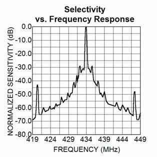
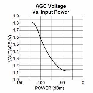
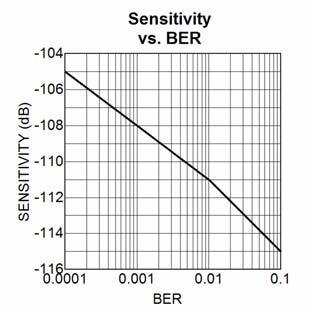
6 Typical Characteristics Sensitivity Graphs Page 6 of 17
7 Functional Diagram Figure 1, CY520 Simplified Block Diagram Functional Description Figure 1. Simplified Block Diagram that illustrates the basic structure of the CY520. It is made of three sub-blocks; Image Rejection UHF Down-converter, the OOK Demodulator, and Reference and Control Logics. Outside the device, the CY520 requires only three components to operate: two capacitors (CTH, and CAGC) and the reference frequency device, usually a quartz crystal. An additional five components may be used to improve performance. These are: power supply decoupling capacitor, two components for the matching network, and two components for the pre-selector band pass filter. Receiver Operation LNA The RF input signal is AC-coupled into the gate circuit of the grounded source LNA input stage. The LNA is a Cascoded NMOS. Mixers and Synthesizer The LO ports of the Mixers are driven by quadrature local oscillator outputs from the synthesizer block. The local oscillator signal from the synthesizer is placed on the low side of the desired RF signal to allow suppression of the image frequency at twice the IF frequency below the wanted signal. The local oscillator is set to 32 times the crystal reference frequency via a phase-locked loop synthesizer with a fully Page 7 of 17
8 integrated loop filter. Image Reject Filter and Band-Pass Filter The IF ports of the mixer produce quadrature down converted IF signals. These IF signals are low-pass filtered to remove higher frequency products prior to the image reject filter where they are combined to reject the image frequencies. The IF signal then passes through a third order band pass filter. The IF center frequency is 1.2MHz. The IF BW is MHz, and this varies with RF operating frequency. The IF BW can be calculated via direct scaling: These filters are fully integrated inside the CY520. After filtering, four active gain controlled amplifier stages enhance the IF signal to proper level for demodulation. OOK Demodulator The demodulator section is comprised of detector, programmable low pass filter, slicer, and AGC comparator. Detector and Programmable Low-Pass Filter The demodulation starts with the detector removing the carrier from the IF signal. Post detection, the signal becomes base band information. The programmable low-pass filter further enhances the base band information. There are four programmable low-pass filter BW settings: 1625Hz, 3250Hz, 6500Hz, 13000Hz for MHz operation. Low pass filter BW will vary with RF Operating Frequency. Filter BW values can be easily calculated by direct scaling. See equation below for filter BW calculation: BW Operating Freq. = It is very important to choose the filter setting that best fits the intended data rate to minimize data distortion. Demod BW is set at MHz as default (assuming both SEL0 and SEL1 pins are floating). The low pass filter can be hardware set by external pins SEL0 and SEL1. SEL0 SEL1 Demod BW (@434MHz) Hz Hz Hz Hz-default Table 1. Demodulation BW Selection Page 8 of 17
9 Slicer, Slicing Level The signal prior to slicer is still linear demodulated AM. Data slicer converts this signal into digital 1 s and 0 s by comparing with the threshold voltage built up on the CTH capacitor. This threshold is determined by detecting the positive and negative peaks of the data signal and storing the mean value. Slicing threshold default is 50%. After the slicer the signal is now digital OOK data. During long periods of 0 s or no data period, threshold voltage on the CTH capacitor may be very low. Large random noise spikes during this time may cause erroneous 1 s at DO pin. AGC Comparator The AGC comparator monitors the signal amplitude from the output of the programmable low-pass filter. When the output signal is less than 750mV thresh-hold, 1.5μA current is sourced into the external CAGC capacitor. When the output signal is greater than 750mV, a 15μA current sink discharges the CAGC capacitor. The voltage developed on the CAGC capacitor acts to adjust the gain of the mixer and the IF amplifier to compensate for RF input signal level variation. Reference Control There are 2 components in Reference and Control sub-block: 1) Reference Oscillator and 2) Control Logic through parallel Inputs: SEL0, SEL1, SHDN Reference Oscillator Figure 2: Reference Oscillator Circuit The reference oscillator in the CY520 (Figure 2) uses a basic Colpitts crystal oscillator configuration with MOS transconductor to provide negative resistance. All capacitors shown in Figure 2 are integrated inside CY520. R01 and R02 are external pins of CY520. User only needs to connect reference oscillation crystal. Page 9 of 17

10 Reference oscillator crystal frequency can be calculated: F REF OSC = F RF / ( /12) For MHz, FREF OSC = MHz To operate the CY520 with minimum offset, crystal frequencies should be specified with 10pF loading capacitance. Application Information Figure 3. CY520 Application Example, MHz The CY520 can be fully tested by using one of many evaluation boards designed at CY for this device. As an entry level, the CY520 (Figure 3) offers a good start for most applications. It has a helical PCB antenna with its matching network, a band-pass-filter front-end as a pre-selector filter, matching network and the minimum components required to make the device work, which are a crystal, Cagc, and Cth capacitors. By removing the matching network of the helical PCB antenna (C9 and L3), a whip antenna (ANT2) or a RF connector (J2) can be used instead. Figure 3 shows the entire schematic of it for MHz. Other frequencies can be used and the values needed are in the tables below. Capacitor C9 and inductor L3 are the passive elements for the helical PCB matching network. A tight tolerance is recommended for these devices, like 2% for the inductor and 0.1pF for the capacitor. PCB variations may require different values and optimization. Table 2 shows the matching elements for the device frequency range. For additional information look for Small PCB Antennas for CY RF Products application note. Table 2. Matching Values for the Helical PCB Antenna Page 10 of 17

11 To use another antenna, like the whip kind, remove C9 and place the whip antenna in the hole provided in the PCB. Also, a RF signal can be injected there. L1 and C8 form the pass-band-filter front-end. Its purpose is to attenuate undesired outside band noise which reduces the receiver performance. It is calculated by the parallel resonance equation f = 1/(2 PI (SQRT L1 C8)). Table 3 shows the most used frequency values. Table 3. Band-Pass-Filter Front-End Values There is no need for the band-pass-filter front-end for applications where it is proven that the outside band noise does not cause a problem. The CY520 has image reject mixers which improve significantly the selectivity and rejection of outside band noise. Capacitor C3 and inductor L2 form the L-shape matching network. The capacitor provides additional attenuation for low frequency outside band noise and the inductor provides additional ESD protection for the antenna pin. Two methods can be used to find these values, which are matched close to 50Ω. One method is done by calculating the values using the equations below and another by using a Smith chart. The latter is made easier by using software that plots the values of the components C8 and L1, like WinSmith by Noble Publishing. To calculate the matching values, one needs to know the input impedance of the device. Table 4 shows the input impedance of the CY520 and suggested matching values for the most used frequencies. These suggested values may be different if the layout is not exactly the same as the one made here. Table 4: matching values for the most used frequencies For the frequency of MHz, the input impedance is Z = 18.6 j174.2ω, then the matching components are calculated by, Equivalent parallel = B = 1/Z = j5.68 msiemens Rp = 1 / Re (B); Xp = 1 / Im (B) Rp = 1.65kΩ; Xp = 176.2Ω Q = SQRT (Rp/50 + 1) Q = Xm = Rp / Q Xm = Ω Page of 17

 for the desired input impedance (Figure 5). We can see the matching leading to the center of the Smith Chart or close to 50Ω. Page - 12 - of 17")
12 Resonance Method For L-shape Matching Network Lc = Xp / (2 Pi f); Lp = Xm / (2 Pi f) L2 = (Lc Lp) / (Lc + Lp); C3 = 1 / (2 Pi f Xm) L2 = 39.8nH C3 = 1.3pF Doing the same calculation example with the Smith Chart, it would appear as follows, First, we plot the input impedance of the device, (Z = MHz (Figure 4). Figure 4: device s input impedance, Z = 18.6 j174.2ω Second, we plot the shunt inductor (39nH) and the series capacitor (1.5pF) for the desired input impedance (Figure 5). We can see the matching leading to the center of the Smith Chart or close to 50Ω. Page of 17

13 Figure 5. Plotting the Shunt Inductor and Series Capacitor Crystal Y1 or Y1A (SMT or leaded respectively) is the reference clock for all the device internal circuits. Crystal characteristics of 10pF load capacitance, 20ppm, ESR < 50Ω, -20ºC to +70ºC temperature range are desired. Table 5 shows the crystal frequencies and one of CY company approved crystal manufacturers. The oscillator of the CY520 is a Colpitts type. It is very sensitive to stray capacitance loads. Thus, very good care must be taken when laying out the printed circuit board. Avoid long traces and ground plane on the top layer close to the REFOSC pins RO1 and RO2. When care is not taken in the layout, and crystals from other vendors are used, the oscillator may take longer times to start as well as the time to good data in the DO pin to show up. In some cases, if the stray capacitance is too high (> 20pF), the oscillator may not start at all. The crystal frequency is calculated by REFOSC = RF Carrier/(32+(1.1/12)). The local oscillator is low side injection ( MHz = MHz), that is, its frequency is below the RF carrier frequency and the image frequency is below the LO frequency. See Figure 6. The product of the incoming RF signal and local oscillator signal will yield the IF frequency, which will be demodulated by the detector of the device. Figure 6. Low Side Injection Local Oscillator. Page of 17

 / 100).")
14 REFOSC (MHz) Carrier (MHz) CY Part Number S M S M S M Table 5. Crystal Frequency and Vendor Part Number. CY520 JP1 and JP2 are the bandwidth selection for the demodulator bandwidth. To set it correctly, it is necessary to know the shortest pulse width of the encoded data sent in the transmitter. Like in the example of the data profile in the figure 7 below, PW2 is shorter than PW1, so PW2 should be used for the demodulator bandwidth calculation which is found by 0.65/shortest pulse width. After this value is found, the setting should be done according to Table 6. For example, if the pulse period is 100μsec, 50% duty cycle, the pulse width will be 50μsec (PW = (100μsec 50%) / 100). So, a bandwidth of 13kHz would be necessary (0.65 / 50μsec). However, if this data stream had a pulse period with 20% duty cycle, the bandwidth required would be 32.5kHz (0.65 / 20μsec), which exceeds the maximum bandwidth of the demodulator circuit. If one tries to exceed the maximum bandwidth, the pulse would appear stretched or wider. Table 6. JP1 and JP2 setting, MHz Other frequencies will have different demodulator bandwidth limits, which are derived from the reference oscillator frequency. Table 7 and Table 8 below shows the limits for the other two most used frequencies. Table 7. JP1 and JP2 setting, MHz Page of 17


15 Table 8. JP1 and JP2 setting, MHz Capacitors C6 and C4, C TH and C AGC respectively provide time base reference for the data pattern received. These capacitors are selected according to data profile, pulse duty cycle, dead time between two received data packets, and if the data pattern has or does not have a preamble. See Figure 7, example of a data Profile. Figure 7. Example of a Data Profile For best results the capacitors should always be optimized for the data pattern used. As the baud rate increases, the capacitor values decrease. Table 9 shows suggested values for Manchester Encoded data, 50% duty cycle. Table 9. Suggested CTH and CAGC Values. Other components used are C5, which is a decoupling capacitor for the V DD line, R4 reserved for future use and not needed for the evaluation board, R3 for the shutdown pin (SHDN=0, device is operation), which can be removed if that pin is connected to a microcontroller or an external switch, R1 and R2 which form a voltage divider for the AGC pin. One can force a voltage in this AGC pin to purposely decrease the device sensitivity. Special care is needed when doing this operation, as an external control of the AGC voltage may vary from lot to lot and may not work the same for several devices. Three other pins are worthy of comment. They are the DO, RSSI, and shut down pins. The DO pin has a driving capability of 0.4mA. This is good enough for most of the logic family ICs in the market today. The RSSI pin provides a transfer function of the RF signal intensity vs voltage. It is very useful to determine the signal to noise ratio of the RF link, crude range estimate from the transmitter source and AM demodulation, Page of 17
.")
16 which requires a low C AGC capacitor value. The shut down pin (SHDN) is useful to save energy. When its level close to V DD (SHDN=1), the device is not in operation. Its DC current consumption is less than 1μA (do not forget to remove R3). When toggling from high to low, there will be a time required for the device to come to steady state mode, and a time for data to shut up in the DO pin. This time will be dependent upon many things such as temperature, crystal used, and if there is an external oscillator with faster startup time. Normally, with the crystal vendors suggested, the data will show up in the DO pin around 1msec time, and 2msec over the temperature range of the device. When using an external oscillator or reference oscillator signal, the time is reduced considerably and can be around 4μsec. See figures Figure10 and 11. Figure 10: Time-to-Good Data After Shut Down Cycle, Room Temperature. Figure 11. Time to Good Data, External Oscillator, Room Temperature. Page of 17
17 Package Information CY520 SOP8 Package Type For more information and assistance, please contact us as follows: CY WIRELESS TECHNOLOGY LIMITED Website: Page of 17
SYN500R Datasheet. ( MHz ASK Receiver) Version 1.0
 Version 1.0") SYN500R Datasheet (300-450MHz ASK Receiver) Version 1.0 Contents 1. General Description... 1 2. Features... 1 3. Applications... 1 4. Typical Application... 2 5. Pin Configuration... 2 6. Pin Description...
SYN500R Datasheet (300-450MHz ASK Receiver) Version 1.0 Contents 1. General Description... 1 2. Features... 1 3. Applications... 1 4. Typical Application... 2 5. Pin Configuration... 2 6. Pin Description...
CY803/802 Datasheet. 300M-450MHz RF receiver CY803/802/802R. General Description. Features. Ordering Information. Typical Application
 CY803/802 Datasheet 300M-450MHz RF receiver General Description The CY803/802 is a general purpose, 3.3-5V, super-heterodyne Receiver that operates from 300M to 450MHz with typical sensitivity of -110dBm.
SYN501R Datasheet. ( MHz Low Voltage ASK Receiver) Version 1.0
 Version 1.0") SYN501R Datasheet (300-450MHz Low Voltage ASK Receiver) Version 1.0 Contents 1. General Description... 1 2. Features... 1 3. Applications... 1 4. Typical Application... 2 5. Pin Configuration... 2 6. Pin
SYN501R Datasheet (300-450MHz Low Voltage ASK Receiver) Version 1.0 Contents 1. General Description... 1 2. Features... 1 3. Applications... 1 4. Typical Application... 2 5. Pin Configuration... 2 6. Pin
Features U1 MICRFAYQS RO1 RO2 GNDRF NC ANT CTH SQ VDD SEL1 SEL0. 315MHz, 1kHz Baud Rate Example
 3.3V, QwikRadio 315MHz Receiver General Description The is a general purpose, 3.3V QwikRadio Receiver that operates at 315MHz with typical sensitivity of -110dBm. The functions as a super-heterodyne receiver
Features U1 MICRF218AYQS 1 RO1 RO2 2 NC 3 GNDRF ANT RSSI 4 +3V VDD CTH 6 IF_BW SEL1 7 DO MHz/ , 900Hz Baud Rate Example
 3.3V, 315/433MHz Wide-IF Bandwidth ASK Receiver General Description The is a 3.0V to 3.6V, 300MHz to 450MHz ASK/OOK super-heterodyne receiver with user selectable Intermediate Frequency (IF) Bandwidths
Features MICRF219AYQS
 General Description 300MHz to 450MHz ASK Receiver with RSSI, Auto-Poll, Bit-Check and Squelch NOT RECOMMENDED REFER TO A FOR NEW DESIGNS Features The is a 300MHz to 450MHz super- 110dBm sensitivity at
Features. Applications. MICRF230 Typical Application Circuit for MHz
 400MHz to 450MHz ASK/OOK Receiver with RSSI and Squelch General Description The is a 400MHz to 450MHz superheterodyne, image-reject, RF receiver with automatic gain control, ASK/OOK demodulator, analog
Features MHz, 1kbps Operation
 300MHz to 450MHz, 3.3V ASK/OOK Receiver with RSSI and Squelch General Description The is a 300MHz to 450MHz superheterodyne, image-reject, RF receiver with automatic gain control, ASK/OOK demodulator,
MHZ APPLICATION EXAMPLE
 Preliminary PT4306 Compact 433.92 MHz OOK/ASK Receiver DESCRIPTION The PT4306 is a compact, fully integrated OOK/ASK receiver for 433.92 MHz frequency band. It requires few external components. The PT4306
Features. MICRF219A Typical Application Circuit (433.92MHz, 1kbps)
") 300MHz to 450MHz ASK/OOK Receiver with Auto-Poll, RSSI, and Squelch General Description The is a 300MHz to 450MHz superheterodyne, image-reject, RF receiver with automatic gain control, ASK/OOK demodulator,
300MHz to 450MHz ASK/OOK Receiver with Auto-Poll, RSSI, and Squelch General Description The is a 300MHz to 450MHz superheterodyne, image-reject, RF receiver with automatic gain control, ASK/OOK demodulator,
The CYF115 transmitter solution is ideal for industrial and consumer applications where simplicity and form factor are important.
 CYF115 Datasheet 300M-450MHz RF Transmitter General Description The CYF115 is a high performance, easy to use, single chip ASK Transmitter IC for remote wireless applications in the 300 to 450MHz frequency
300~440MHz ASK/OOK Receiver General Description
 RF83A/RF83C 300~440MHz ASK/OOK Receiver General Description The RF83A/RF83C is a single chip ASK/OOK (ON- OFF Keyed) RF receiver IC. This device is a true antenna-in to data-out monolithic device. All
Features +5V ASK DATA INPUT. 1.0pF. 8.2pF. 10nH. 100pF. 27nH. 100k. Figure 1
 QwikRadio UHF ASK Transmitter Final General Description The is a single chip Transmitter IC for remote wireless applications. The device employs s latest QwikRadio technology. This device is a true data-in,
RADIO MODULE MXR-220S UHF AM TRANSCEIVER MODULE PRELIMINARY DATA SHEET. Radios, Inc. June 14, 2010 Preliminary Data Sheet
 RADIO MODULE DATA SHEET Radios, Inc. June 14, 2010 Preliminary Data Sheet The is a general purpose transceiver module that operates at 433.92MHz with typical sensitivity of -110dBm and is inteded for use
SYN113 Datasheet. ( MHz ASK Transmitter) Version 1.0
 Version 1.0") Datasheet (300 450MHz ASK Transmitter) Version 1.0 Contents 1. General Description... 1 2. Features... 1 3. Applications... 1 4. Typical Application... 2 5. Pin Configuration... 2 6. Pin Description...
Datasheet (300 450MHz ASK Transmitter) Version 1.0 Contents 1. General Description... 1 2. Features... 1 3. Applications... 1 4. Typical Application... 2 5. Pin Configuration... 2 6. Pin Description...
CYF115H Datasheet. 300M-450MHz ASK transmitter CYF115H FEATURES DESCRIPTION APPLICATIONS
 CYF115H Datasheet 300M-450MHz ASK transmitter FEATURES 12V High Voltage Supply Internal LDO Regulator 300MHz to 450MHz Frequency Range Data Rates up to 10kbps ASK Output Power to 17dBm on 50ohm load Low
Applications MICRF229. Supports bit rates. No IF filter required. bit rates up to. package 40 C to +105 C. temperaturee range.
 400MHz to 450MHz ASK/OOK Receiver with Auto-Poll and RSSI General Description The is a 400MHz to 450MHz super- control, ASK/OOKK demodulator, and analog RSSI output. It only requires a crystal and a minimum
Features. Applications. 387 MHz, 1200 BAUD OOK RECEIVER
 Receiver/Data Demodulator Advance Information General Description The is a single chip OOK (ON-OFF Keyed) Receiver IC for remote wireless applications, employing s latest technology. This device is a true
The SYN400R is a fully featured part in 16-pin packaging, the SYN410R is the same part packaged in 8-pin packaging with a reduced feature set.
 Contents 1. General Description... 1 2. Features... 1 3. Applications... 1 4. Typical Application... 2 5. Ordering Information... 2 6. Pin Configuration... 2 7. 8-Pin Options... 3 8. Pin Description...
Features. MICRF219A Typical Application Circuit (433.92MHz, 1kbps)
") 300MHz to 450MHz ASK/OOK Receiver with Auto-Poll, and RSSI General Description The is a 300MHz to 450MHz superheterodyne, image-reject, RF receiver with automatic gain control, ASK/OOK demodulator, and
300MHz to 450MHz ASK/OOK Receiver with Auto-Poll, and RSSI General Description The is a 300MHz to 450MHz superheterodyne, image-reject, RF receiver with automatic gain control, ASK/OOK demodulator, and
RX3400 Low Power ASK Receiver IC. Description. Features. Applications. Block Diagram
 Low Power ASK Receiver IC Princeton Technology Corp. reserves the right to change the product described in this datasheet. All information contained in this datasheet is subject to change without prior
315MHz Low-Power, +3V Superheterodyne Receiver
 General Description The MAX1470 is a fully integrated low-power CMOS superheterodyne receiver for use with amplitude-shiftkeyed (ASK) data in the 315MHz band. With few required external components, and
RX3400 Low Power ASK Receiver IC. Description. Features. Applications. Block Diagram
 Low Power ASK Receiver IC the wireless IC company HiMARK Technology, Inc. reserves the right to change the product described in this datasheet. All information contained in this datasheet is subject to
EVALUATION KIT AVAILABLE 300MHz to 450MHz High-Efficiency, Crystal-Based +13dBm ASK Transmitter 3.0V. 100nF DATA INPUT
 19-31; Rev 4; /11 EVALUATION KIT AVAILABLE 300MHz to 450MHz High-Efficiency, General Description The crystal-referenced phase-locked-loop (PLL) VHF/UHF transmitter is designed to transmit OOK/ASK data
DESCRIPTION FEARURES. Applications
 FEARURES Complete UHF transmitter 450MHz to 1000MHz Frequency Range Data Rates up to 10kbps ASK Output Power to 10dBm on 50ohm load Low external part count Operate with Crystals or Ceramic Resonators SOT23-6
Applications RF83L. RF83L 300~440MHz ASK/OOK. Receiver V1.0
 Receiver V1.0 RF83L 300~440MHz ASK/OOK RF 83 L 300 MHz - 440 M Hz ASK/OOK Receiver -------------------------------------------------------------------------------------------------------------------------------------------------------------------------------------------------------------------------------
300MHz to 450MHz High-Efficiency, Crystal-Based +13dBm ASK Transmitter
 EVALUATION KIT AVAILABLE MAX044 General Description The MAX044 crystal-referenced phase-locked-loop (PLL) VHF/UHF transmitter is designed to transmit OOK/ASK data in the 300MHz to 450MHz frequency range.
Low Power 315/433 MHz OOK/ASK Superheterodyne PT4316 Receiver with SAW-based Oscillator DESCRIPTION
 Low Power 315/433 MHz OOK/ASK Superheterodyne DESCRIPTION The is a very low power consumption single chip OOK/ASK superheterodyne receiver for the 315MHz and 434MHz frequency bands and which offers a high
315MHz/434MHz ASK Superheterodyne Receiver
 General Description The MAX7034 fully integrated low-power CMOS superheterodyne receiver is ideal for receiving amplitude-shiftkeyed (ASK) data in the 300MHz to 450MHz frequency range (including the popular
MICRF007 VSS REFOSC ANT CAGC +5V VDD SHUT. 315MHz 1200b/s On-Off Keyed Receiver
 MICRF007 QwikRadio Low-Power UHF Receiver General Description The MICRF007 is a single chip, ON-OFF Keyed (ASK/OOK) Receiver for remote wireless applications, employing s latest QwikRadio technology. This
RF83/RF83C 300~440MHz ASK/OOK Receiver
 RF83/RF83C 300~440MHz ASK/OOK Receiver General Description The RF83/RF83C is a single chip ASK/OOK (ON-OFF Keyed) RF receiver IC. This device is a true antenna-in to data-out monolithic device. All RF
Package and Pin Assignment SSOP-6 (0.64mm pitch) OSCIN OSCOUT TXEN 3 VSS 4 TXOUT 5 VSS 6 7 MODIN 8 HiMARK SW DO RES RESB VREFP VSS Symbol
 OSCIN OSCOUT TXEN 3 VSS 4 TXOUT 5 VSS 6 7 MODIN 8 HiMARK SW DO RES RESB VREFP VSS Symbol") Low Power ASK Transmitter IC HiMARK Technology, Inc. reserves the right to change the product described in this datasheet. All information contained in this datasheet is subject to change without prior
Low Power ASK Transmitter IC HiMARK Technology, Inc. reserves the right to change the product described in this datasheet. All information contained in this datasheet is subject to change without prior
QwikRadio Low-Power UHF Receiver. Features. Applications. Operating Mode Shutdown Package. MICRF010BM MICRF010YM Fixed Yes 8-pin SOIC
 QwikRadio Low-Power UHF Receiver General Description The is a single chip, ASK/OOK (ON-OFF Keyed) RF receiver IC recommended for new designs replacing the MICRF007. It provides the same function with sensitivity
MICRF113. Features. General Description. Applications. Ordering Information. 300MHz to 450MHz +10dBm ASK Transmitter in SOT23
 300MHz to 450MHz +10dBm ASK Transmitter in SOT23 General Description The is a high-performance, easy-to-use, singlechip ASK Transmitter IC for remote wireless applications in the 300MHz to 450MHz frequency
QwikRadio Low-Power UHF Receiver. Features. Applications
 QwikRadio Low-Power UHF Receiver General Description The is a single chip, ASK/OOK (ON-OFF Keyed) RF receiver IC. It provides the same function but with performance enhancements over earlier QwikRadio
MICRF007. General Description. Features. Applications. Typical Application. QwikRadio Low-Power UHF Receiver Preliminary Information
 MICRF007 QwikRadio Low-Power UHF Receiver Preliminary Information General Description The MICRF007 is a single chip ASK/OOK (ON-OFF Keyed) Receiver IC for remote wireless applications, employing s latest
RCR-XXX-RP. Features. Typical Applications. Description. - i - Low cost 315/418/ MHz Super-Regen ASK/OOK Receiver
 RCR-XXX-RP Embedding the wireless future.. Low cost 315/418/433.92 MHz Super-Regen ASK/OOK Receiver Typical Applications Features Remote Keyless Entry (RKE) Remote Lighting Controls On-Site Paging Asset
ISM Band FSK Receiver IC ADF7902
 ISM Band FSK Receiver IC FEATURES Single-chip, low power UHF receiver Companion receiver to ADF7901 transmitter Frequency range: 369.5 MHz to 395.9 MHz Eight RF channels selectable with three digital inputs
Low Power 315/ MHz OOK Receiver
 CMT2210LCW Low Power 315/433.92 MHz OOK Receiver Features Operation Frequency: 315 / 433.92 MHz OOK Demodulation Data Rate: 1.0-5.0 kbps Sensitivity: -109 dbm (3.0 kbps, 0.1% BER) Receiver Bandwidth: 330
MICRF003 / 033. QwikRadio tm 900 MHz UHF Receiver. Preliminary Information
 / 033 900 MHz UHF Receiver Preliminary Information General Description The is a single chip OOK (ON-OFF Keyed) Receiver IC for remote wireless applications, employing s latest technology. This device is
Features. Applications
 QwikRadio UHF ASK/FSK Transmitter General Description The is a high performance, easy to use, single chip ASK / FSK Transmitter IC for remote wireless applications in the 300 to 450MHz frequency band.
Low-Voltage IF Transceiver with Limiter/RSSI and Quadrature Modulator
 19-1296; Rev 2; 1/1 EVALUATION KIT MANUAL FOLLOWS DATA SHEET Low-Voltage IF Transceiver with General Description The is a highly integrated IF transceiver for digital wireless applications. It operates
Applications Note RF Transmitter and Antenna Design Hints
 This application note covers the TH7107,TH71071,TH71072,TH7108,TH71081,TH72011,TH72031,TH7204 Single Frequency Transmitters. These transmitters have different features and cover different bands but they
DESCRIPTIO FEATURES APPLICATIO S. LT GHz to 2.7GHz Receiver Front End TYPICAL APPLICATIO
 1.GHz to 2.GHz Receiver Front End FEATURES 1.V to 5.25V Supply Dual LNA Gain Setting: +13.5dB/ db at Double-Balanced Mixer Internal LO Buffer LNA Input Internally Matched Low Supply Current: 23mA Low Shutdown
SG2525A SG3525A REGULATING PULSE WIDTH MODULATORS
 SG2525A SG3525A REGULATING PULSE WIDTH MODULATORS 8 TO 35 V OPERATION 5.1 V REFERENCE TRIMMED TO ± 1 % 100 Hz TO 500 KHz OSCILLATOR RANGE SEPARATE OSCILLATOR SYNC TERMINAL ADJUSTABLE DEADTIME CONTROL INTERNAL
MICRF011. QwikRadio tm Receiver/Data Demodulator. Preliminary Information. Features
 Receiver/Data Demodulator Preliminary Information General Description The, an enhanced version of the MICRF001, is a single chip OOK (ON-OFF Keyed) Receiver IC for remote wireless applications, employing
MICRF002 / 022. QwikRadio tm Low Power UHF Receiver. Preliminary Information. Features
 / 022 Low Power UHF Receiver Preliminary Information General Description The, an enhanced version of the MICRF001 and MICRF011, is a single chip OOK (ON-OFF Keyed) Receiver IC for remote wireless applications,
315MHz/433MHz ASK Superheterodyne Receiver with AGC Lock
 General Description The MAX7033 fully integrated low-power CMOS superheterodyne receiver is ideal for receiving amplitude shiftkeyed (ASK) data in the 300MHz to 450MHz frequency range. The receiver has
FM Radio Transmitter & Receiver Modules
 Features Miniature SIL package Fully shielded Data rates up to 128kbits/sec Range up to 300 metres Single supply voltage Industry pin compatible T5-434 Temp range -20 C to +55 C No adjustable components
TOP VIEW V DD DATAOUT
 19-4386; Rev 1; 8/10 EVALUATION KIT AVAILABLE 300MHz to 450MHz ASK Receiver General Description The low-cost receiver is designed to receive amplitude-shift-keyed (ASK) and on-off-keyed (OOK) data in the
APPLICATION NOTE 3671 Data Slicing Techniques for UHF ASK Receivers
 Maxim > Design Support > Technical Documents > Application Notes > Basestations/Wireless Infrastructure > APP 3671 Maxim > Design Support > Technical Documents > Application Notes > Wireless and RF > APP
Features. Applications
 300-440MHz QwikRadio ASK Receiver General Description The MICRF002 is a single chip ASK/OOK (ON-OFF Keyed) RF receiver IC. This device is a true antenna-in to data-out monolithic device. All RF and IF
Features. Future Electronics (
 / ASB Embedding the wireless future.. Low-Cost SAW-stabilized surface mount OOK RF transmitter Typical Applications Remote Keyless Entry (RKE) Remote Lighting Controls On-Site Paging Asset Tracking Wireless
Features MICRF102 REFOSC STBY. 100k +5V. Figure 1
 MIRF02 MIRF02 QwikRadio UHF ASK Transmitter Final Information General Description The MIRF02 is a single chip Transmitter I for remote wireless applications. The device employs s latest QwikRadio technology.
Low-Jitter, 8kHz Reference Clock Synthesizer Outputs MHz
 19-3530; Rev 0; 1/05 Low-Jitter, 8kHz Reference General Description The low-cost, high-performance clock synthesizer with an 8kHz input reference clock provides six buffered LVTTL clock outputs at 35.328MHz.
Features. Haltronics Ltd (http://www.haltronicsltd.com/)
") Embedding the wireless future.. Low-Cost SAW-stabilized surface mount OOK RF transmitter Typical Applications Remote Keyless Entry (RKE) Remote Lighting Controls On-Site Paging Asset Tracking Wireless
Embedding the wireless future.. Low-Cost SAW-stabilized surface mount OOK RF transmitter Typical Applications Remote Keyless Entry (RKE) Remote Lighting Controls On-Site Paging Asset Tracking Wireless
Value Units -0.3 to +4.0 V -50 to
 Designed for Short-Range Wireless Data Communications Supports 2.4-19.2 kbps Encoded Data Transmissions 3 V, Low Current Operation plus Sleep Mode Ready to Use OEM Module The DR3100 transceiver module
DESCRIPTION FEATURES APPLICATIONS BLOCK DIAGRAM. PT MHz / MHz PLL Tuned Low Power FSK Receiver
 315 MHz / 433.92 MHz PLL Tuned Low Power FSK Receiver DESCRIPTION The PT4305 is a PLL-tuned FSK receiver for short-range wireless data applications in the 315 MHz and 434 MHz frequency bands. The PT4305
Features MICRF002 VDDRF VDDBB +5V WAKEB SHUT uF. 315MHz 800bps On-Off Keyed Receiver
 MICRF002/RF022 300-440MHz QwikRadio ASK Receiver Final Information General Description The MICRF002 is a single chip ASK/OOK (ON-OFF Keyed) RF receiver IC. This device is a true antenna-in to data-out
DESCRIPTIO APPLICATIO S. LTC5531 Precision 300MHz to 7GHz RF Detector with Shutdown and Offset Adjustment FEATURES TYPICAL APPLICATIO
 LTC553 Precision 3MHz to 7GHz RF Detector with Shutdown and Offset Adjustment FEATURES Temperature Compensated Internal Schottky Diode RF Detector Wide Input Frequency Range: 3MHz to 7GHz* Wide Input Power
Type Ordering Code Package TDA Q67000-A5168 P-DIP-18-5
 Video Modulator for FM-Audio TDA 5666-5 Preliminary Data Bipolar IC Features FM-audio modulator Sync level clamping of video input signal Controlling of peak white value Continuous adjustment of modulation
CYSR805 Datasheet. General Description: MHz RF receiver. Application. Package drawing. Features CYSR805
 Datasheet 250-450MHz RF receiver CYSR805 General Description: CYSR805 is a single chip Super Regenerative Receiver(SRR) RF IC. CYSR805 is composed of an low noise pre-amplifier, the super regenerative
433MHz Single Chip RF Transmitter
 433MHz Single Chip RF Transmitter nrf402 FEATURES True single chip FSK transmitter Few external components required On chip UHF synthesiser No set up or configuration 20kbit/s data rate 2 channels Very
Low-voltage mixer FM IF system
 DESCRIPTION The is a low-voltage monolithic FM IF system incorporating a mixer/oscillator, two limiting intermediate frequency amplifiers, quadrature detector, logarithmic received signal strength indicator
Remote keyless entry After market alarms. Wireless point of sale. Si4312 DOUT DSP MCU BASEBAND PROCESSOR SQUELCH RATIO 315/434 TH[1:0] BT[1:0] RST
![Remote keyless entry After market alarms. Wireless point of sale. Si4312 DOUT DSP MCU BASEBAND PROCESSOR SQUELCH RATIO 315/434 TH[1:0] BT[1:0] RST](/thumbs/72/66414919.jpg "Remote keyless entry After market alarms. Wireless point of sale. Si4312 DOUT DSP MCU BASEBAND PROCESSOR SQUELCH RATIO 315/434 TH[1:0] BT[1:0] RST") 315/433.92 MHZ OOK RECEIVER Features Single chip receiver with only six external components Selectable 315/433.92 MHz carrier frequency Supports OOK modulation High sensitivity ( 110dBm @ 1.0kbps) Frequency
315/433.92 MHZ OOK RECEIVER Features Single chip receiver with only six external components Selectable 315/433.92 MHz carrier frequency Supports OOK modulation High sensitivity ( 110dBm @ 1.0kbps) Frequency
Direct battery operation with onchip low drop out (LDO) voltage. 16 MHz crystal oscillator support. Remote keyless entry After market alarms
 voltage. 16 MHz crystal oscillator support. Remote keyless entry After market alarms") 315/433.92 MHZ FSK RECEIVER Features Single chip receiver with only six Data rates up to 10 kbps external components Direct battery operation with onchip low drop out (LDO) voltage Selectable 315/433.92
315/433.92 MHZ FSK RECEIVER Features Single chip receiver with only six Data rates up to 10 kbps external components Direct battery operation with onchip low drop out (LDO) voltage Selectable 315/433.92
Features. Slope Comp Reference & Isolation
 MIC388/389 Push-Pull PWM Controller General Description The MIC388 and MIC389 are a family of complementary output push-pull PWM control ICs that feature high speed and low power consumption. The MIC388/9
DESCRIPTIO APPLICATIO S. LTC5530 Precision 300MHz to 7GHz RF Detector with Shutdown and Gain Adjustment FEATURES TYPICAL APPLICATIO
 Precision 3MHz to 7GHz RF Detector with Shutdown and Gain Adjustment FEATURES Temperature Compensated Internal Schottky Diode RF Detector Wide Input Frequency Range: 3MHz to 7GHz* Wide Input Power Range:
Single chip 433MHz RF Transceiver
 Single chip 433MHz RF Transceiver RF0433 FEATURES True single chip FSK transceiver On chip UHF synthesiser, 4MHz crystal reference 433MHz ISM band operation Few external components required Up to 10mW
FM Radio Transmitter & Receiver Modules
 FM Radio Transmitter & Receiver Modules T5 / R5 Features Miniature SIL package Fully shielded Data rates up to 128kbits/sec Range up to 300 metres Single supply voltage Industry pin compatible QFMT5-434
SF229 Low Power PIR Circuit IC For security applications
 Low Power PIR Circuit IC For security applications Preliminary datasheet DESCRIPTION The SF229 is a low power CMOS mixed signal ASIC designed for battery powered security applications that are either hard
Data Sheet for the AS3922 Half-Duplex 868/915 MHz Transceiver
 AS3922 Half Duplex 868/915 MHzTranceiver Data Sheet Data Sheet for the AS3922 Half-Duplex 868/915 MHz Transceiver Data Sheet Rev. A1, April 2001 AS3922 Single Chip High Performance RF Transceiver Applications
Low Distortion Mixer AD831
 a FEATURES Doubly-Balanced Mixer Low Distortion +2 dbm Third Order Intercept (IP3) + dbm 1 db Compression Point Low LO Drive Required: dbm Bandwidth MHz RF and LO Input Bandwidths 2 MHz Differential Current
LW MHz / 433 MHz ASK Receiver Preliminary Data Sheet Rev 0.3, August, 2006
 Introduction The LW106 is a superheterodyne amplitude-shift-keying (ASK) modulation (or On-Off keying, OOK) single chip receiver. It is designed to operate for low power device (LPD) applications. Industry
Parameters Symbol Min. Typ. Max. Unit Condition Frequency Range Output Frequency Range f MHz
 Features Any frequency between 1 MHz and 110 MHz accurate to 6 decimal places Operating temperature from -40 C to +85 C. Refer to MO2018 for -40 C to +85 C option and MO2020 for -55 C to +125 C option
RF2667. Typical Applications CDMA/FM Cellular Systems CDMA PCS Systems GSM/DCS Systems
 RF66 RECEIVE AGC AND DEMODULATOR Typical Applications CDMA/FM Cellular Systems CDMA PCS Systems GSM/DCS Systems TDMA Systems Spread Spectrum Cordless Phones Wireless Local Loop Systems Product Description
Low voltage LNA, mixer and VCO 1GHz
 DESCRIPTION The is a combined RF amplifier, VCO with tracking bandpass filter and mixer designed for high-performance low-power communication systems from 800-1200MHz. The low-noise preamplifier has a
Si4356. Si4356 STANDALONE SUB-GHZ RECEIVER. Features. Applications. Description
 STANDALONE SUB-GHZ RECEIVER Features Pin configurable Frequency range = 315 917 MHz Supply Voltage = 1.8 3.6 V Receive sensitivity = Up to 113 dbm Modulation (G)FSK OOK Applications Low RX Current = 12
Advanced Regulating Pulse Width Modulators
 Advanced Regulating Pulse Width Modulators FEATURES Complete PWM Power Control Circuitry Uncommitted Outputs for Single-ended or Push-pull Applications Low Standby Current 8mA Typical Interchangeable with
RF Monolithics, Inc. Complies with Directive 2002/95/EC (RoHS) Electrical Characteristics. Reference Crystal Parameters
 Electrical Characteristics. Reference Crystal Parameters") Complies with Directive 00//EC (RoHS) I. Product Overview TXC0 is a rugged, single chip ASK/FSK Transmitter IC in the 300-0 MHz frequency range. This chip is highly integrated and has all required RF functions
Complies with Directive 00//EC (RoHS) I. Product Overview TXC0 is a rugged, single chip ASK/FSK Transmitter IC in the 300-0 MHz frequency range. This chip is highly integrated and has all required RF functions
Features MIC2193BM. Si9803 ( 2) 6.3V ( 2) VDD OUTP COMP OUTN. Si9804 ( 2) Adjustable Output Synchronous Buck Converter
 6.3V ( 2) VDD OUTP COMP OUTN. Si9804 ( 2) Adjustable Output Synchronous Buck Converter") MIC2193 4kHz SO-8 Synchronous Buck Control IC General Description s MIC2193 is a high efficiency, PWM synchronous buck control IC housed in the SO-8 package. Its 2.9V to 14V input voltage range allows
MIC2193 4kHz SO-8 Synchronous Buck Control IC General Description s MIC2193 is a high efficiency, PWM synchronous buck control IC housed in the SO-8 package. Its 2.9V to 14V input voltage range allows
MCU with 315/433/868/915 MHz ISM Band Transmitter Module
 MCU with 315/433/868/915 MHz ISM Band Transmitter Module (The purpose of this RFM60 spec covers mainly for the hardware and RF parameter info of the module, for MCU and software info please refer to RF60
FAN MHz TinyBoost Regulator with 33V Integrated FET Switch
 FAN5336 1.5MHz TinyBoost Regulator with 33V Integrated FET Switch Features 1.5MHz Switching Frequency Low Noise Adjustable Output Voltage Up to 1.5A Peak Switch Current Low Shutdown Current:
Application Note Receivers MLX71120/21 With LNA1-SAW-LNA2 configuration
 Designing with MLX71120 and MLX71121 receivers using a SAW filter between LNA1 and LNA2 Scope Many receiver applications, especially those for automotive keyless entry systems require good sensitivity
UNISONIC TECHNOLOGIES CO., LTD
 U UNISONIC TECHNOLOGIES CO., LTD REGULATING PWM IC DESCRIPTION The UTC U is a pulse width modulator IC and designed for switching power supplies application to improve performance and reduce external parts
EUP V/12V Synchronous Buck PWM Controller DESCRIPTION FEATURES APPLICATIONS. Typical Application Circuit. 1
 5V/12V Synchronous Buck PWM Controller DESCRIPTION The is a high efficiency, fixed 300kHz frequency, voltage mode, synchronous PWM controller. The device drives two low cost N-channel MOSFETs and is designed
DR7000-EV MHz. Transceiver Evaluation Module
 Designed for Short-Range Wireless Data Communications Supports RF Data Transmission Rates Up to 115.2 kbps 3 V, Low Current Operation plus Sleep Mode Up to 10 mw Transmitter Power The DR7000-EV hybrid
PART 20 IF_IN LO_V CC 10 TANK 11 TANK 13 LO_GND I_IN 5 Q_IN 6 Q_IN 7 Q_IN 18 V CC
 19-0455; Rev 1; 9/98 EALUATION KIT AAILABLE 3, Ultra-Low-Power Quadrature General Description The combines a quadrature modulator and quadrature demodulator with a supporting oscillator and divide-by-8
Features. RAMP Feed Forward Ramp/ Volt Sec Clamp Reference & Isolation. Voltage-Mode Half-Bridge Converter CIrcuit
 MIC3838/3839 Flexible Push-Pull PWM Controller General Description The MIC3838 and MIC3839 are a family of complementary output push-pull PWM control ICs that feature high speed and low power consumption.
Range ANTP ANTN STBY. 100k +5V
 MICRF02 QwikRadio UHF ASK Transmitter General Description The MICRF02 is a single chip Transmitter IC for remote wireless applications. The device employs s latest QwikRadio technology. This device is
Data Sheet for the AS3921 Half-Duplex 315/433 MHz Transceiver
 Half Duplex 315/433 MHz Tranceiver AS3921 Data Sheet for the AS3921 Half-Duplex 315/433 MHz Transceiver Data Sheet Rev. A1, April 2001 AS3921 Single Chip High Performance RF Transceiver Applications UHF
Low Distortion Mixer AD831
 Low Distortion Mixer AD831 FEATURES Doubly Balanced Mixer Low Distortion +24 dbm Third Order Intercept (IP3) +1 dbm 1 db Compression Point Low LO Drive Required: 1 dbm Bandwidth 5 MHz RF and LO Input Bandwidths
SN W Mono Filterless Class-D Audio Power Amplifier DESCRIPTION FEATURES APPLICATIONS. Typical Application Circuit
 2.6W Mono Filterless Class-D Audio Power Amplifier DESCRIPTION The SN200 is a 2.6W high efficiency filter-free class-d audio power amplifier in a.5 mm.5 mm wafer chip scale package (WCSP) that requires
Phase-locked loop PIN CONFIGURATIONS
 NE/SE DESCRIPTION The NE/SE is a versatile, high guaranteed frequency phase-locked loop designed for operation up to 0MHz. As shown in the Block Diagram, the NE/SE consists of a VCO, limiter, phase comparator,
NTE7047 Integrated Circuit TV Color Small Signal Sub System
 NTE7047 Integrated Circuit TV Color Small Signal Sub System Features: Vision IF Amplifier with Synchronous Demodulator Automatic Gain Control (AGC) Detector Suitable for Negative Modulation AGC Tuner Automatic
1GHz low voltage LNA, mixer and VCO
 DESCRIPTION The is a combined RF amplifier, VCO with tracking bandpass filter and mixer designed for high-performance low-power communication systems from 800-1200MHz. The low-noise preamplifier has a
3A, 23V, 380KHz Step-Down Converter
 3A, 23V, 380KHz Step-Down Converter General Description The is a buck regulator with a built in internal power MOSFET. It achieves 3A continuous output current over a wide input supply range with excellent
FM Transmitter Module
 FM Transmitter Module XT5 Features MINIATURE SIL PACKAGE FULLY SHIELDED DATA RATES UP TO 128KBITS/S 5v 10mW 3v 10mW versions available TYPICAL RANGE 350+ m (433.92 MHz Version) 433.92 MHz VERSIONS INDUSTRY
PARAMETER CONDITIONS TYPICAL PERFORMANCE Operating Supply Voltage 3.1V to 3.5V Supply Current V CC = 3.3V, LO applied 152mA
 DESCRIPTION LT5578 Demonstration circuit 1545A-x is a high linearity upconverting mixer featuring the LT5578. The LT 5578 is a high performance upconverting mixer IC optimized for output frequencies in
RT9285A/B. Tiny Package, High Performance, Diode Embedded White LED Driver. Preliminary. Features. General Description.
 General Description The RT9285 is a high frequency asynchronous boost converter with internal diode, which can support 2 to 5 White LEDs for backlighting and OLED power supply. The Internal soft start