Analog and Telecommunication Electronics
|
|
|
- Jonas McKinney
- 5 years ago
- Views:
Transcription
1 Politecnico di Torino - ICT School Analog and Telecommunication Electronics F1 - Power devices» Schottky and pin diodes» MOS, BJT, IGBT, TRIAC» Safe Operating Area» Thermal analysis 06/06/ ATLCE - F DDC
2 Lesson F1: Power devices Models and parameters for Diodes, PIN, Schottky Zener diodes MOS, BJT, IGBT, SCR, TRIAC Operating limits Safe Operating Area Power dissipation Thermal analysis Reference: Book 1: ch 3, ch 4, ch 5, ch 14 06/06/ ATLCE - F DDC
3 Relevant parameters for power devices Voltage Sustain high voltages Current Handle high current Power Deliver high power to the load, Low dissipated power and temperature rise on control device High efficiency Speed High frequency (RF not here) Fast switching 06/06/ ATLCE - F DDC
4 Power devices Diodes Standard P-I-N Schottky Zener Transistors BJT MOS-FET IGBT SCR/TRIAC Subsystems Voltage reference, voltage regulators,. group G 06/06/ ATLCE - F DDC
5 Power device applications Switches Two-state devices» ON /OFF state Power switches Signal switches Amplifier & linear applications Analog devices Continuous control output V or I from input V or I Provide power gain» Low input control power Extremes of operation range: ON/OFF states 06/06/ ATLCE - F DDC
6 Switch operation Command signal ON state Short circuit, zero voltage drop (Low resistance, low voltage drop) Control OFF state Open circuit, zero current (High resistance, low current) V I Dynamic (state transition) Types: Mechanical/ Electronic 06/06/ ATLCE - F DDC
7 Switch parameters ON state Ideal: Short circuit, zero voltage drop Actual:» Low resistance Ron» low voltage drop Vsat OFF state Ideal: Open circuit, zero current Actual:» High resistance» Low current (leakage) Ioff Power dissipation Ideal: 0 Actual: not 0 06/06/ ATLCE - F DDC
8 Switch parameters Command signal type (V, I, mechanical, ) Vmax Max voltage OFF state (Vbrk) Imax Max current ON state Pd dissipated power (Max, actual) Tc switching time Delay from command to actual state change ON OFF and ON OFF Direction of V and I Num of cycles Environmental (temp, vibration, radiation, ) EMI (speed of change dv/dt, di/dt) 06/06/ ATLCE - F DDC
9 Mechanical switches Mobile metal contact Open/closed Command signal: Force (finger, coil, other mechancal) Vmax Max voltage OFF state (Vbrk): Contact spacing Imax Max current ON state: Contact size Tc switching time: Mechanical time constant Strong points Low Ron, low Ioff, low power loss Able to handle high V and I Critical issues Number of cycles Arching, Bouncing Delay from command to actual state change 06/06/ ATLCE - F DDC
10 Electronic switches Diodes Two-terminal devices Control on same pins as Power flow (output) ON/OFF controlled by applied V and I Transistors and other devices (DIAC, TRIAC, ) At least 3 pins Separate control signal 06/06/ ATLCE - F DDC
11 Review of pn Junctions Density gradient cause diffusion of majority charge carriers across the junction. These carriers combine with (and remove) carriers of opposite polarity. free p carriers (holes) free n carriers (electrones) No free carrier here: depletion layer (insulator) free carriers available: conductor 06/06/ ATLCE - F DDC
12 Biased pn Junction Forward bias p-type side positive with respect to n-type side thin depletion layer If forward bias voltage higher than a threshold majority charge carriers can move through the junction current flow, which increases with the voltage Reverse bias p-type side negative with respect to the n-type side wide depletion layer less majority charge carriers through the junction (same amount of minority carriers) small leakage current caused by minority carriers 06/06/ ATLCE - F DDC
13 Semiconductor junction model In a diode current can flow only in one direction Ideal, or first approximation model I = Is (too small to be seen) conduction voltage p n Turn-on voltage (threshold) 06/06/ ATLCE - F DDC
14 I(V) characteristic of sem. junction pn junction current I: I S : leakage current reverse current, for V<0 I D V ηv I T 1 s e V: applied voltage V T kt e e: electron charge, k: Boltzmann s constant, T: absolute temperature, η: a constant in the range 1 to 2 (we assume =1) kt At 25 C: V T 26 mv e Resistive behavior for high currents 06/06/ ATLCE - F DDC
15 Diode ON state Near threshold Exponential characteristic High currents Resistance of low-doping material and contact Linear V,I Current (Is) related with temperature» Exponential dependence Current concentration in small area» Hot spots Get wide effective active junction cross-section» Multiple parallel device» Current distribution + Positive feedback 06/06/ ATLCE - F DDC
16 Diode OFF: reverse breakdown The junction cannot sustain too high reverse voltage For V > Vbr insulating layer is broken, and current increases Two types of breakdown Zener breakdown A very high field strength across the junction pulls electrons through the junction, causing large reverse current. Zener breakdown normally occurs below 5 V. Avalanche breakdown Field strength is sufficient to accelerate the electrons; Electrons collide with atoms, and liberate other electrons, (avalanche effect) Avalanche breakdown usually occurs at voltages > 5 V 06/06/ ATLCE - F DDC
17 Linear model and parameters Imax: Max direct current ΔV/ΔI = Ron: ON resistance Is: reverse current (leakage) Vbr (Vzk) Breakdown voltage Von: ON voltage drop Figure 3.8 The diode i v relationship with some scales expanded and others compressed in order to reveal details. 06/06/ ATLCE - F DDC

18 Diode equivalent circuits Straight-line models, with different approximation. 06/06/ ATLCE - F DDC
19 Silicon diode parameters Turn-on voltage about 0.5 V Considered ON when I > I S Conduction voltage about 0.7 V depends on current, higher for high currents Breakdown voltage depends on device construction 40 V (small-signal) 400 V (power) 4 kv (High Voltage) Max current depends on device construction 100 ma (signal) many A (power) a few ka (High Current) Leakage current Is depends on Material, temperature, device type,»na ma 06/06/ ATLCE - F DDC
20 Comparison of diode parameters Description General Purpose Rectifier Fast Switching Rectifier Small Signal Diode Schottky Diode Sample Device 1N4001 1N4933 1N4148 ZC2800 Maximum DC/Average Forward Current 1 A 1 A 300 ma 15 ma Maximum Reverse Voltage 50 V 50 V 75 V 70 V Reverse Leak. 25 C, VR = 20 V 50 na 200 na 5 na 200 na Forward Voltage ~0.7 V 1 IF = 1A 1 IF = 10 ma ma 06/06/ ATLCE - F DDC
21 Device data sheet example 06/06/ ATLCE - F DDC
22 Increasing reverse breakdown voltage Breakdown comes from high E-field E=V/x Reduce the E-field same V, increase x (distance) Decrease doping to get wider depletion layer (increase x )» Worse parameters in ON state Decrease doping only in a narrow layer: PIN diodes p-intrinsic (insulator)-n junction (PIN diode): OFF state:» Can sustain very high inverse voltages (kv). ON state» Higher losses in the conductive region. 06/06/ ATLCE - F DDC
23 PIN diodes Applications of PIN diodes: radio frequency switches and attenuators. radiation detectors and photodetectors. power electronics (central layer can withstand high voltages) PIN structure used also in other power semiconductors: IGBTs, power MOSFETs, thyristors, The intrinsic layer increases breakdown voltage Drawbacks Higher ON resistance Higher threshold voltage ( 1 V) 06/06/ ATLCE - F DDC
24 Pin diode band diagram 06/06/ ATLCE - F DDC
25 ON OFF ON transients (ideal) Vi positive Direct bias, ON Current can flow Id Vi Vd Vi Id Reverse bias: Id = 0; Vd = Vi Vi negative Reverse bias, OFF Vd t No current Actual transient depends on parasitic capacitances and charges in the junction ON: charges are stored in the junction region ON OFF: charges must be removed OFF ON: faster transient Forward bias: Vd = 0,6V Id = Vi/R 06/06/ ATLCE - F DDC
26 Junction in the transient Forward bias: a large number of electrons/holes injected into the p/n-material, Switching to reverse bias: Stored minority carriers must return to the opposite material. Storage time ts: current reverses and stays at a constant level. Electrons and holes diffuse and recombine Transition time Tt: current decreases to the reverse current Is Ts + Tt = Trr: reverse recovery time. During trr the diode dissipates energy high frequecy applications diodes with short trr. higher forward voltage drop and higher reverse currents. 06/06/ ATLCE - F DDC
27 ON OFF ON transient (actual) ON OFF OFF ON Vi Id t rr Vd t s t t t 90% final Forward bias Id = Is t rf Minority carrier storage removal Id = Vi/R RC transient 06/06/ ATLCE - F DDC
28 Switching parameters ON OFF Charges stored in the junction must be removed Reverse current flow» High losses (for a short time)» Qrr: reverse injected charge» Trr: reverse recovery time» Irr: reverse peak current OFF ON Faster than ON OFF Relevant timing parameter:» Trf (recovery forward)» Much faster that Trr 06/06/ ATLCE - F DDC
29 Schottky diodes Schottky junction Metal - Si (light doping, if heavy doping becomes a contact) Conduction based on majority carriers (from metal) Benefits: No charge storage in depletion region Fast switch Lower threshold voltage and direct drop (0,3 V), less Pd Schottky junctions used to speed-up BJT circuits (logic ICs) Drawbacks High capacitance (OFF state) Low reverse voltage (<100V) High reverse current (temperature-dependent) 06/06/ ATLCE - F DDC
30 Comparison of diode parameters Description General Purpose Rectifier Fast Switching Rectifier Small Signal Diode Schottky Diode Sample Device 1N4001 1N4933 1N4148 ZC2800 Maximum DC/Average Forward Current 1 A 1 A 300 ma 15 ma Maximum Reverse Voltage 50 V 50 V 75 V 70 V Reverse Leak. 25 C, VR = 20 V 50 na 200 na 5 na 200 na Forward Voltage ~0.7 V 1 IF = 1A 1 IF = 10 ma ma Rev Rec Time Trr 2 μs 200 ns 4 ns < 1 ns Cost 20 cent 15 cent 25 cent 100 cent 06/06/ ATLCE - F DDC
31 Data sheet Schottky diode 06/06/ ATLCE - F DDC
32 Schottky junction in logic circuits Schottky junctions are used also for BJT to avoid saturation and increase speed (no reverse recovery). The Shottky junction is placed from B to C; as C voltage goes below B, the diode steers current away from B, and avoids transistor saturation Embedded in gate structure for logic circuits 06/06/ ATLCE - F DDC
33 Zener diodes All junctions have breakdown Breakdowns usually change junction parameters to worse values (high local heating, modification of doping) Some devices are designed to operate in breakdown without degradation: ZENER diodes Used for Protection circuits Low power voltage regulators Cheap reference voltage sources 06/06/ ATLCE - F DDC
34 Zener diode i(v) characteristic Iz and Vz have inverse sign from Id, Vd of standard diodes I Z V Z Figure 3.21 The diode i v characteristic with the breakdown region shown in some detail. 06/06/ ATLCE - F DDC
35 Zener diode equivalent circuit Vzo: Vz for I = 0 (linear model) I Rz Rz: ΔV/ΔI (actually differential rz) V + Vzo Izmin: minimum current to exit knee region I Pdmax (or Izmax): limited by temperature rise V 06/06/ ATLCE - F DDC
36 Zener diode applications The reverse breakdown voltage can be used to get a voltage reference Breakdown voltage becomes the Zener voltage, Vz Output voltage of circuit shown is equal to Vz, despite variations in input voltage V A resistor is used to limit the current in the diode Discussed in detail in the voltage regulator section. 06/06/ ATLCE - F DDC
37 Zener diode operating point Select I, V sign as for diodes Draw characterisitc of left-side bipole (Vs + R) + Rs Vsu I V Draw Dz I(V) characteristic Operating point at intersection I Evaluate effect of Vsu or Rs changes Vsu/Rs V If Dz operates in breakdown Vo regulation Vsu 06/06/ ATLCE - F DDC
38 Diode circuit analysis The non-linear behavior of diodes makes analysis more difficult Correct: Solve system with nonlinear equations E I I S V D (e V k V R Approximated: D ) V D IR Use linear piecewise model, with two-step analysis» Evaluate ON/OFF switching point» Use separate models for each state 06/06/ ATLCE - F DDC
39 Diode circuits: power rectifier One application of diodes is in rectification half-wave rectifier 4 diodes full wave rectifier Evaluate with different models Effects of leakage current Is Effect of voltage drop on the junction Effect of diode series resistance 06/06/ ATLCE - F DDC
40 Diode circuits: AC DC conversion Half-wave rectifier capacitor used to produce a steadier output Vi is AC Vo is almost DC Basic AC-DC converter (power supply) 06/06/ ATLCE - F DDC
 + HPF (remove DC) Also known as")

41 Diode circuits: signal rectifier Used to demodulate AM signals: AC DC + LPF (smooth) + HPF (remove DC) Also known as an envelope detector Found in a wide range of radio receivers, from crystal sets to superheterodynes. 06/06/ ATLCE - F DDC
42 Diode circuits: signal clamping A simple form of signal conditioning Circuits limit the excursion of the voltage waveform Can use a combination of signal and Zener diodes. 06/06/ ATLCE - F DDC
43 Diode circuits: over-voltage protection When switch is open, the inductor tries to make current continue to flow. large back e.m.f. arcing in mechanical switches, breakdown in electronic switches Catch diode low impedance path to dissipate the energy stored in the inductor» SW closed: diode reverse-biased, no current flow» SW opens: the current in L continue to flow through the diode 06/06/ ATLCE - F DDC
44 Lesson D1: Power devices Models and parameters for Diodes, PIN, Schottky Zener diodes MOS, BJT, IGBT, SCR, TRIAC Operating limits Safe Operating Area Power dissipation Thermal analysis Reference: Book 1 (Sedra): ch 3, ch 4, ch 5, ch 14 06/06/ ATLCE - F DDC
45 Power BJT devices Use vertical technology More current in the same area (higher density) Most relevant parameters (for power circuits): Vcebr C-E breakdown voltage Icmax max collector current β current gain Vcesat C-E voltage drop in saturation I c Thermal parameters» Max power, Thermal resistance Fundamental relation: Ic= β Ib I b V be V ce 06/06/ ATLCE - F DDC
46 Vertical power BJT structure Vertical BJT doping density ( cm^-1) Low doping in base region Wide depletion layer, high brk voltage Low current gain (5 20) High transit time Ft < 10 MHz B E n P 10^16 N 10^14 N+ 10^19 Primary breakdown Avalanche carrier multiplication in the BC junction Secondary breakdown High current in small area (same problem as diodes)» Multiple small devices with current sharing Critical region: Near saturation, high power deep saturation (low β) C 06/06/ ATLCE - F DDC
 model of the npn transistor.")
47 BJT model Ebers-Moll model for BJT Simplified models BE diode + Ic source Ic = β Ib Linear models» Hybrid»Gm» Figure 5.8 The Ebers-Moll (EM) model of the npn transistor. 06/06/ ATLCE - F DDC
48 Switch or amplifier? Use as amplifier Active region Use as switch ON Saturation Use as switch OFF Cutoff 06/06/ ATLCE - F DDC
49 BJT as a switch Operating points are on the load line 06/06/ ATLCE - F DDC
50 BJT operation The current gain β decreases for high currents Need significant driving power Operation is based on minority carriers Slow dynamic Temperature dependence To increase BVceo, base region long and lightly doped Higher epsilon Reduced E field Higher recombination probability Lower current gain High voltage devices have low current gain 06/06/ ATLCE - F DDC
51 Safe Operating Area Limits to Current Voltage Power 06/06/ ATLCE - F DDC
52 Saturation model for BJT V source Vcesat (0.1 V) Series resistor Rcesat (few ohms) Lower Vcesat with C-E inversion (lower β) 06/06/ ATLCE - F DDC
53 Critical saturation region Low current gain (5 20) Critical region: Near saturation, high Ic, residual Vce high power dissipation Design solution Guarantee deep saturation (high Ib drive) Use Darlington connections» Single integrated structure» Npn-npn» Npn-pnp 06/06/ ATLCE - F DDC
54 Darlington devices 06/06/ ATLCE - F DDC
55 Cutoff model for BJT Ib = 0 Ic = 0 (ideal) BC junction leakage current: Icbo If base open, enters as Ib, causing Iceo = β Icbo Iceo causes power dissipation Temperature rise high leakage current temperature rise Thermal runaway Avoid high current density areas (hot spot) Multiple devices, with current partition Steer Icbo away from Base R to GND Reverse bias BE (without breakdown!) 06/06/ ATLCE - F DDC
 Current rating is a function of the channel W & L A vertical structure can")
56 Power MOS-FET Planar structure Low power devices Current and breakdown voltage ratings function of the channel W & L. Vertical structure Voltage rating function of doping and thickness of N-epitaxial layer (vertical) Current rating is a function of the channel W & L A vertical structure can sustain both high V & I 06/06/ ATLCE - F DDC
57 MOS-FET parasitics The vertical structure creates a pn junction from body (S) to substrate (D) S G D Current can always flow from S to D A 1-quadrant switch 4-quadrant with two MOS 06/06/ ATLCE - F DDC
58 MOS-FET parasitics The vertical structure creates also a parasitic transistor 06/06/ ATLCE - F DDC
59 MOS-FET parameters Basic parameters: Vdsbr D-S Breakdown voltage Idmax Max Drain current Vgsth Threshold voltage Rdson ON equivalent resistance Qg total charge injected into the Gate (for a given Vgs) A power transistor may consist of several cells (thousands) Power MOS DMOS,. (double-diffused metal oxide semiconductor) Power MOSFETs are made using this technology 06/06/ ATLCE - F DDC
60 MOS-FET model Model depends on operating point Low Vgs (subthreshold):» Exponential Medium Vgs:» Square law High Vgs:» linear Figure Typical i D v GS characteristic for a power MOSFET. 06/06/ ATLCE - F DDC
")
61 MOS-FET output characteristic Warning! Saturation in MOS has a different meaning (called active region in BJT) 06/06/ ATLCE - F DDC
62 MOS-FET switching models ON: Equivalent resistance Ron OFF: Leakage current Ioff Dynamic GS capacitance DS capacitance Parasitic towards substrate 06/06/ ATLCE - F DDC
63 MOS-FET gate charge Before threshold: Cgs Active region Miller effect on Cgd Saturation Cgd 06/06/ ATLCE - F DDC
64 MOS-FET vs BJT MOS-FET use majority carriers High switching speed Reduced temperature dependence MOSFET use simpler driving circuit The Gate represents a plate of a capacitor (towards GND); no current after first charging step, but Need to drive a high-capacitance load for fast switching ON state BJT modeled as Vcesat (+Ron) MOS modeled as Ron OFF state: BJT and MOS modeled as current source (leakage) 06/06/ ATLCE - F DDC
65 Four-layer devices Transistors have limitations in switching high currents at high voltages Other devices are specifically designed for such applications: four-layer devices Specific physical structure Can be used only as switches (not for linear amplifiers) A great deal in common with bipolar transistors SCR/Tyristor TRIAC/DIAC 06/06/ ATLCE - F DDC
66 4-layer device operation Circuit with two interconnected BJTs Turning on T2 provides Ic2 as Ib1 to T1, and Ic1 as Ib2. Both devices conducts until the current goes to zero. The two BJTs can be built as a single 4-layer device Tyristor or Silicon Controlled Rectifier (SCR) 06/06/ ATLCE - F DDC
67 SCR in CMOS logic circuits SCR structure intrinsic in CMOS ICs Responsible for latch up Triggered by Input levels out of GND-Vcc range High energy particles pmosfet nmosfet V G DD S D D G S V SS p+ p+ n+ n+ n+ p+ T1 p-well T2 n-substrate 06/06/ ATLCE - F DDC
68 The thyristor Four-layer device with a pnpn structure Three terminals: anode, cathode and gate Gate is the control input. Power flow between Anode and Cathode 06/06/ ATLCE - F DDC
69 Thyristor in AC power control Triggered ON by a pulse on the Gate Stays ON as long as V > 0 (remainder of the half cycle) Returns OFF when V = 0 Varying firing time changes output power Single-wave allows control from 0 50% of full power 06/06/ ATLCE - F DDC
70 The Triac and the Diac A bidirectional thyristor Allows full-wave control using a single device Often used with a diac: bidirectional trigger diode to produce the gate drive pulses The DIAC breaks down at a particular voltage and fires the triac 06/06/ ATLCE - F DDC
71 A simple lamp-dimmer using a triac Current pulse to fire the Triac Phase shift network. Provides trigger voltage for Diac 06/06/ ATLCE - F DDC
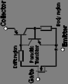
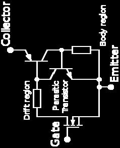
72 IGBT The Insulated Gate Bipolar Transistor or IGBT combines bipolar and MOS devices MOSFET gate-drive + high Ic and low Vcesat of BJT isolated gate FET for the control input, bipolar power transistor as a switch, in a single device combines high efficiency and fast switching. Used in medium- to high-power applications switching power supply, motor control, induction heating, Large IGBT modules (many devices in parallel), can handle» high current k 100 A» High voltages k 1000 V. 06/06/ ATLCE - F DDC


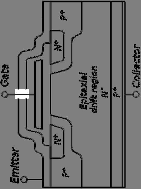
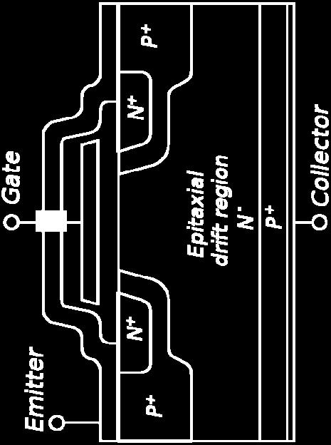
73 IGBT structure 06/06/ ATLCE - F DDC
74 IGBT characteristic 06/06/ ATLCE - F DDC
75 Lesson F1: Power devices Models and parameters for Diodes, PIN, Schottky Zener diodes MOS, BJT, IGBT, SCR, TRIAC Operating limits Safe Operating Area Power dissipation Thermal analysis 06/06/ ATLCE - F DDC
76 Operating limits Breakdown voltage If higher, insulating layers are broken Max current If higher, wires or conducting paths can melt Max power Power dissipation causes temperature rise Max temperature Doping distribution is modified changes in parameters Silicon itself can melt Special application parameters Radiation in space,. 06/06/ ATLCE - F DDC
77 Safe Operating Area Any electronic devices can handle limited power, voltage, current For active devices, the region of acceptable V,I is the Safe Operating Area (SOA), defined by Power limit (V x I > Pdmax)» Excess power cause temperature rise, with melting» Secondary breakdown: local heating and thermal runaway Voltage (V < Vbrk)» Excess voltage causes breakdown and insulator perforation Current (I < Imax)» Excess current cause heating and metal evaporation 06/06/ ATLCE - F DDC
78 Safe Operating Area boundaries Too high current Too high V x I (power) - not uniform current flow - high local power dissipation Active & Safe Operating Area (SOA) Too high voltage 06/06/ ATLCE - F DDC
79 SOA for BJT (TIP31) Includes dynamic behavior Pdmax depends on pulse Duty Cycle Log scale! I x V = K is a straigth line 06/06/ ATLCE - F DDC
80 SOA for MOS (IRF640) Dynamic behavior Log scale No secondary breakdown Id limited by Rds 06/06/ ATLCE - F DDC
81 Power dissipation All electric devices dissipate a power Pd = V I Power dissipation increases temperature Any device has temperature limits, therefore power limits The effects of power dissipation can be modeled using thermal equivalent circuits Power current Temperature node voltage Heat conduction capability thermal resistance θr ( /W) Diodes/MOS/BJT power dissipated on the junctions Heat must be brought outside, through a path including» Junction-case defined by manufacturer» Case-ambient controlled using heat sinks 06/06/ ATLCE - F DDC
82 Power derating Manufacturers specify Max power dissipation Pdmax Max junction operating temperature Tjmax Power dissipation causes temperature rise Allowed power dissipation decreases with Ta Ta = Tjmax Pd = 0 06/06/ ATLCE - F DDC
83 Evaluation of temperature rise Electric network model for thermal behaviour Power Pd current source Temperature T node voltage Heat conduction θ thermal resistance θr ( /W) Electrical equivalent circuit Tj Ta = Pd θja 06/06/ ATLCE - F DDC
84 From junction to ambient The thermal path from junctin to ambient consists of: Junction-Case: θ JC» Thermal resistance defined by the package Case-heatsink: θ CS» Case and fixture Heatsink-ambient: θ SA» Heatsink and operating condition (air flow) Designer can control θ CS and θ SA 06/06/ ATLCE - F DDC

85 Thermal specification Power devices specified for No heatsink, Ta specified, Tc? infinite heatsink, Tc = Ta Example datasheet TIP30 06/06/ ATLCE - F DDC
86 Power BJT datasheet (TIP31) 06/06/ ATLCE - F DDC
87 Power MOS datasheet IRF640 06/06/ ATLCE - F DDC
88 Heatsink datasheet example 06/06/ ATLCE - F DDC

89 Dynamic thermal response 06/06/ ATLCE - F DDC
90 Lesson F1: summary Describe the dynamic behavior of pn junctions. Which are the benefits of PIN diodes vs standard diodes? Which are the benefits of Schottky junctions? Draw at least 3 models for semiconductor diodes. What is secondary breakdown? Draw a model for power BJT. Describe differences of low/high power MOSFETs. Which parameters defines the boundary of SOA? How can we evaluate the actual temperature of a power semiconductor junction? Define the infinite heatsink concept. 06/06/ ATLCE - F DDC
Analog and Telecommunication Electronics
 Politecnico di Torino - ICT School Analog and Telecommunication Electronics F2 Active power devices»mos»bjt» IGBT, TRIAC» Safe Operating Area» Thermal analysis 30/05/2012-1 ATLCE - F2-2011 DDC Lesson F2:
Analog and Telecommunication Electronics
 Politecnico di Torino - ICT School Analog and Telecommunication Electronics F3 - Actuator driving» Driving BJT switches» Driving MOS-FET» SOA and protection» Smart switches 29/06/2011-1 ATLCE - F3-2011
Power Semiconductor Devices
 TRADEMARK OF INNOVATION Power Semiconductor Devices Introduction This technical article is dedicated to the review of the following power electronics devices which act as solid-state switches in the circuits.
Lecture Note on Switches Marc T. Thompson, 2003 Revised Use with gratefulness for ECE 3503 B term 2018 WPI Tan Zhang
 Lecture Note on Switches Marc T. Thompson, 2003 Revised 2007 Use with gratefulness for ECE 3503 B term 2018 WPI Tan Zhang Lecture note on switches_tan_thompsonpage 1 of 21 1. DEVICES OVERVIEW... 4 1.1.
Power Electronics. P. T. Krein
 Power Electronics Day 10 Power Semiconductor Devices P. T. Krein Department of Electrical and Computer Engineering University of Illinois at Urbana-Champaign 2011 Philip T. Krein. All rights reserved.
SRM INSTITUTE OF SCIENCE AND TECHNOLOGY (DEEMED UNIVERSITY)
") SRM INSTITUTE OF SCIENCE AND TECHNOLOGY (DEEMED UNIVERSITY) QUESTION BANK I YEAR B.Tech (II Semester) ELECTRONIC DEVICES (COMMON FOR EC102, EE104, IC108, BM106) UNIT-I PART-A 1. What are intrinsic and
SRM INSTITUTE OF SCIENCE AND TECHNOLOGY (DEEMED UNIVERSITY) QUESTION BANK I YEAR B.Tech (II Semester) ELECTRONIC DEVICES (COMMON FOR EC102, EE104, IC108, BM106) UNIT-I PART-A 1. What are intrinsic and
Analog Electronic Circuits
 Analog Electronic Circuits Chapter 1: Semiconductor Diodes Objectives: To become familiar with the working principles of semiconductor diode To become familiar with the design and analysis of diode circuits
CONTENTS. 2.2 Schrodinger's Wave Equation 31. PART I Semiconductor Material Properties. 2.3 Applications of Schrodinger's Wave Equation 34
 CONTENTS Preface x Prologue Semiconductors and the Integrated Circuit xvii PART I Semiconductor Material Properties CHAPTER 1 The Crystal Structure of Solids 1 1.0 Preview 1 1.1 Semiconductor Materials
QUESTION BANK EC6201 ELECTRONIC DEVICES UNIT I SEMICONDUCTOR DIODE PART A. It has two types. 1. Intrinsic semiconductor 2. Extrinsic semiconductor.
 FATIMA MICHAEL COLLEGE OF ENGINEERING & TECHNOLOGY Senkottai Village, Madurai Sivagangai Main Road, Madurai - 625 020. [An ISO 9001:2008 Certified Institution] QUESTION BANK EC6201 ELECTRONIC DEVICES SEMESTER:
Solid State Devices- Part- II. Module- IV
 Solid State Devices- Part- II Module- IV MOS Capacitor Two terminal MOS device MOS = Metal- Oxide- Semiconductor MOS capacitor - the heart of the MOSFET The MOS capacitor is used to induce charge at the
EE70 - Intro. Electronics
 EE70 - Intro. Electronics Course website: ~/classes/ee70/fall05 Today s class agenda (November 28, 2005) review Serial/parallel resonant circuits Diode Field Effect Transistor (FET) f 0 = Qs = Qs = 1 2π
Reg. No. : Question Paper Code : B.E./B.Tech. DEGREE EXAMINATION, NOVEMBER/DECEMBER Second Semester
 WK 5 Reg. No. : Question Paper Code : 27184 B.E./B.Tech. DEGREE EXAMINATION, NOVEMBER/DECEMBER 2015. Time : Three hours Second Semester Electronics and Communication Engineering EC 6201 ELECTRONIC DEVICES
Field Effect Transistors (npn)
") Field Effect Transistors (npn) gate drain source FET 3 terminal device channel e - current from source to drain controlled by the electric field generated by the gate base collector emitter BJT 3 terminal
Field Effect Transistors (npn) gate drain source FET 3 terminal device channel e - current from source to drain controlled by the electric field generated by the gate base collector emitter BJT 3 terminal
Lesson 5. Electronics: Semiconductors Doping p-n Junction Diode Half Wave and Full Wave Rectification Introduction to Transistors-
 Lesson 5 Electronics: Semiconductors Doping p-n Junction Diode Half Wave and Full Wave Rectification Introduction to Transistors- Types and Connections Semiconductors Semiconductors If there are many free
UNIT 3: FIELD EFFECT TRANSISTORS
 FIELD EFFECT TRANSISTOR: UNIT 3: FIELD EFFECT TRANSISTORS The field effect transistor is a semiconductor device, which depends for its operation on the control of current by an electric field. There are
Fundamentals of Power Semiconductor Devices
 В. Jayant Baliga Fundamentals of Power Semiconductor Devices 4y Spri ringer Contents Preface vii Chapter 1 Introduction 1 1.1 Ideal and Typical Power Switching Waveforms 3 1.2 Ideal and Typical Power Device
UNIT I POWER SEMI-CONDUCTOR DEVICES
 UNIT I POWER SEMI-CONDUCTOR DEVICES SUBJECT CODE SUBJECT NAME STAFF NAME : EE6503 : Power Electronics : Ms.M.Uma Maheswari 1 SEMICONDUCTOR DEVICES POWER DIODE POWER TRANSISTORS POWER BJT POWER MOSFET IGBT
UNIT-1 Bipolar Junction Transistors. Text Book:, Microelectronic Circuits 6 ed., by Sedra and Smith, Oxford Press
 UNIT-1 Bipolar Junction Transistors Text Book:, Microelectronic Circuits 6 ed., by Sedra and Smith, Oxford Press Figure 6.1 A simplified structure of the npn transistor. Microelectronic Circuits, Sixth
FIELD EFFECT TRANSISTOR (FET) 1. JUNCTION FIELD EFFECT TRANSISTOR (JFET)
 1. JUNCTION FIELD EFFECT TRANSISTOR (JFET)") FIELD EFFECT TRANSISTOR (FET) The field-effect transistor (FET) is a three-terminal device used for a variety of applications that match, to a large extent, those of the BJT transistor. Although there
FIELD EFFECT TRANSISTOR (FET) The field-effect transistor (FET) is a three-terminal device used for a variety of applications that match, to a large extent, those of the BJT transistor. Although there
Power Electronics Power semiconductor devices. Dr. Firas Obeidat
 Power Electronics Power semiconductor devices Dr. Firas Obeidat 1 Table of contents 1 Introduction 2 Classifications of Power Switches 3 Power Diodes 4 Thyristors (SCRs) 5 The Triac 6 The Gate Turn-Off
UNIT I PN JUNCTION DEVICES
 UNIT I PN JUNCTION DEVICES 1. Define Semiconductor. 2. Classify Semiconductors. 3. Define Hole Current. 4. Define Knee voltage of a Diode. 5. What is Peak Inverse Voltage? 6. Define Depletion Region in
VALLIAMMAI ENGINEERING COLLEGE SRM Nagar, Kattankulathur
 VALLIAMMAI ENGINEERING COLLEGE SRM Nagar, Kattankulathur 603 203. DEPARTMENT OF ELECTRONICS & COMMUNICATION ENGINEERING SUBJECT QUESTION BANK : EC6201 ELECTRONIC DEVICES SEM / YEAR: II / I year B.E.ECE
EC6202-ELECTRONIC DEVICES AND CIRCUITS YEAR/SEM: II/III UNIT 1 TWO MARKS. 1. Define diffusion current.
 EC6202-ELECTRONIC DEVICES AND CIRCUITS YEAR/SEM: II/III UNIT 1 TWO MARKS 1. Define diffusion current. A movement of charge carriers due to the concentration gradient in a semiconductor is called process
2 Marks - Question Bank. Unit 1- INTRODUCTION
 Two marks 1. What is power electronics? EE6503 POWER ELECTRONICS 2 Marks - Question Bank Unit 1- INTRODUCTION Power electronics is a subject that concerns the applications electronics principles into situations
4.2.2 Metal Oxide Semiconductor Field Effect Transistor (MOSFET)
") 4.2.2 Metal Oxide Semiconductor Field Effect Transistor (MOSFET) The Metal Oxide Semitonductor Field Effect Transistor (MOSFET) has two modes of operation, the depletion mode, and the enhancement mode.
4.2.2 Metal Oxide Semiconductor Field Effect Transistor (MOSFET) The Metal Oxide Semitonductor Field Effect Transistor (MOSFET) has two modes of operation, the depletion mode, and the enhancement mode.
Experiment (1) Principles of Switching
 Principles of Switching") Experiment (1) Principles of Switching Introduction When you use microcontrollers, sometimes you need to control devices that requires more electrical current than a microcontroller can supply; for this,
Experiment (1) Principles of Switching Introduction When you use microcontrollers, sometimes you need to control devices that requires more electrical current than a microcontroller can supply; for this,
R a) Draw and explain VI characteristics of Si & Ge diode. (8M) b) Explain the operation of SCR & its characteristics (8M)
 Draw and explain VI characteristics of Si & Ge diode. (8M) b) Explain the operation of SCR & its characteristics (8M)") SET - 1 1. a) Define i) transient capacitance ii) Diffusion capacitance (4M) b) Explain Fermi level in intrinsic and extrinsic semiconductor (4M) c) Derive the expression for ripple factor of Half wave
SET - 1 1. a) Define i) transient capacitance ii) Diffusion capacitance (4M) b) Explain Fermi level in intrinsic and extrinsic semiconductor (4M) c) Derive the expression for ripple factor of Half wave
Student Lecture by: Giangiacomo Groppi Joel Cassell Pierre Berthelot September 28 th 2004
 Student Lecture by: Giangiacomo Groppi Joel Cassell Pierre Berthelot September 28 th 2004 Lecture outline Historical introduction Semiconductor devices overview Bipolar Junction Transistor (BJT) Field
SYED AMMAL ENGINEERING COLLEGE
 SYED AMMAL ENGINEERING COLLEGE (Approved by the AICTE, New Delhi, Govt. of Tamilnadu and Affiliated to Anna University, Chennai) Established in 1998 - An ISO 9001:2008 Certified Institution Dr. E.M.Abdullah
Module 04.(B1) Electronic Fundamentals
 Electronic Fundamentals") 1.1a. Semiconductors - Diodes. Module 04.(B1) Electronic Fundamentals Question Number. 1. What gives the colour of an LED?. Option A. The active element. Option B. The plastic it is encased in. Option
1.1a. Semiconductors - Diodes. Module 04.(B1) Electronic Fundamentals Question Number. 1. What gives the colour of an LED?. Option A. The active element. Option B. The plastic it is encased in. Option
SGP100N09T. Symbol Parameter SGP100N09T Unit. 70* -Continuous (TA = 100 )
") SUPER-SEMI SUPER-MOSFET Super Gate Metal Oxide Semiconductor Field Effect Transistor 100V Super Gate Power Transistor SG*100N09T Rev. 1.01 Jun. 2016 SGP100N09T 100V N-Channel MOSFET Description The SG-MOSFET
SUPER-SEMI SUPER-MOSFET Super Gate Metal Oxide Semiconductor Field Effect Transistor 100V Super Gate Power Transistor SG*100N09T Rev. 1.01 Jun. 2016 SGP100N09T 100V N-Channel MOSFET Description The SG-MOSFET
I E I C since I B is very small
 Figure 2: Symbols and nomenclature of a (a) npn and (b) pnp transistor. The BJT consists of three regions, emitter, base, and collector. The emitter and collector are usually of one type of doping, while
Unit III FET and its Applications. 2 Marks Questions and Answers
 Unit III FET and its Applications 2 Marks Questions and Answers 1. Why do you call FET as field effect transistor? The name field effect is derived from the fact that the current is controlled by an electric
Appendix: Power Loss Calculation
 Appendix: Power Loss Calculation Current flow paths in a synchronous buck converter during on and off phases are illustrated in Fig. 1. It has to be noticed that following parameters are interrelated:
MTLE-6120: Advanced Electronic Properties of Materials. Semiconductor transistors for logic and memory. Reading: Kasap
 MTLE-6120: Advanced Electronic Properties of Materials 1 Semiconductor transistors for logic and memory Reading: Kasap 6.6-6.8 Vacuum tube diodes 2 Thermionic emission from cathode Electrons collected
 VALLIAMMAI ENGINEERING COLLEGE SRM NAGAR, KATTANKULATHUR- 603 203 DEPARTMENT OF ELECTRONICS AND COMMUNICATION ENGINEERING EC6202- ELECTRONIC DEVICES AND CIRCUITS UNIT I PN JUNCTION DEVICES 1. Define Semiconductor.
IGBTs (Insulated Gate Bipolar Transistor)
") IGBTs (Insulated Gate Bipolar Transistor) Description This document describes the basic structures, ratings, and electrical characteristics of IGBTs. It also provides usage considerations for IGBTs. 1
IGBTs (Insulated Gate Bipolar Transistor) Description This document describes the basic structures, ratings, and electrical characteristics of IGBTs. It also provides usage considerations for IGBTs. 1
ECE:3410 Electronic Circuits
 ECE:3410 Electronic Circuits Output Stages and Power Amplifiers Sections of Chapter 8 A. Kruger Power + Output Stages1 Power Amplifiers, Power FETS & BJTs Audio (stereo) MP3 Players Motor controllers Servo
DOWNLOAD PDF POWER ELECTRONICS DEVICES DRIVERS AND APPLICATIONS
 Chapter 1 : Power Electronics Devices, Drivers, Applications, and Passive theinnatdunvilla.com - Google D Download Power Electronics: Devices, Drivers and Applications By B.W. Williams - Provides a wide
FET(Field Effect Transistor)
") Field Effect Transistor: Construction and Characteristic of JFETs. Transfer Characteristic. CS,CD,CG amplifier and analysis of CS amplifier MOSFET (Depletion and Enhancement) Type, Transfer Characteristic,
Field Effect Transistor: Construction and Characteristic of JFETs. Transfer Characteristic. CS,CD,CG amplifier and analysis of CS amplifier MOSFET (Depletion and Enhancement) Type, Transfer Characteristic,
Questions on JFET: 1) Which of the following component is a unipolar device?
 Which of the following component is a unipolar device?") Questions on JFET: 1) Which of the following component is a unipolar device? a) BJT b) FET c) DJT d) EFT 2) Current Conduction in FET takes place due e) Majority charge carriers only f) Minority charge
Questions on JFET: 1) Which of the following component is a unipolar device? a) BJT b) FET c) DJT d) EFT 2) Current Conduction in FET takes place due e) Majority charge carriers only f) Minority charge
Semiconductor Devices
 Semiconductor Devices Modelling and Technology Source Electrons Gate Holes Drain Insulator Nandita DasGupta Amitava DasGupta SEMICONDUCTOR DEVICES Modelling and Technology NANDITA DASGUPTA Professor Department
Department of Electrical Engineering IIT Madras
 Department of Electrical Engineering IIT Madras Sample Questions on Semiconductor Devices EE3 applicants who are interested to pursue their research in microelectronics devices area (fabrication and/or
Basic Electronics. Introductory Lecture Course for. Technology and Instrumentation in Particle Physics Chicago, Illinois June 9-14, 2011
 Basic Electronics Introductory Lecture Course for Technology and Instrumentation in Particle Physics 2011 Chicago, Illinois June 9-14, 2011 Presented By Gary Drake Argonne National Laboratory Session 3
Device Technologies. Yau - 1
 Device Technologies Yau - 1 Objectives After studying the material in this chapter, you will be able to: 1. Identify differences between analog and digital devices and passive and active components. Explain
NAME: Last First Signature
 UNIVERSITY OF CALIFORNIA, BERKELEY College of Engineering Department of Electrical Engineering and Computer Sciences EE 130: IC Devices Spring 2003 FINAL EXAMINATION NAME: Last First Signature STUDENT
Analog Electronics. Electronic Devices, 9th edition Thomas L. Floyd Pearson Education. Upper Saddle River, NJ, All rights reserved.
 Analog Electronics BJT Structure The BJT has three regions called the emitter, base, and collector. Between the regions are junctions as indicated. The base is a thin lightly doped region compared to the
COLLECTOR DRAIN BASE GATE EMITTER. Applying a voltage to the Gate connection allows current to flow between the Drain and Source connections.
 MOSFETS Although the base current in a transistor is usually small (< 0.1 ma), some input devices (e.g. a crystal microphone) may be limited in their output. In order to overcome this, a Field Effect Transistor
Power MOSFET Basics. Table of Contents. 2. Breakdown Voltage. 1. Basic Device Structure. 3. On-State Characteristics
 Power MOSFET Basics Table of Contents P-body N + Source Gate N - Epi 1. Basic Device Structure 2. Breakdown Voltage 3. On-State Characteristics 4. Capacitance 5. Gate Charge 6. Gate Resistance 7. Turn-on
ECE520 VLSI Design. Lecture 2: Basic MOS Physics. Payman Zarkesh-Ha
 ECE520 VLSI Design Lecture 2: Basic MOS Physics Payman Zarkesh-Ha Office: ECE Bldg. 230B Office hours: Wednesday 2:00-3:00PM or by appointment E-mail: pzarkesh@unm.edu Slide: 1 Review of Last Lecture Semiconductor
Lecture 2 - Overview of power switching devices. The Power Switch: what is a good power switch?
 Lecture 2 - Overview of power switching devices The Power Switch: what is a good power switch? A K G Attributes of a good power switch are: 1. No power loss when ON 2. No power loss when OFF 3. No power
55:041 Electronic Circuits
 55:041 Electronic Circuits Output Stages and Power Amplifiers Sections of Chapter 8 A. Kruger Power + Output Stages1 Power Amplifiers, Power FETS & BJTs Audio (stereo) MP3 Players Motor controllers Servo
10. Output Stages and Power Supplies. 10. Output Stages and Power Supplies TLT-8016 Basic Analog Circuits 2005/2006 1
 10. Output Stages and Power Supplies 10. Output Stages and Power Supplies TLT-8016 Basic Analog Circuits 2005/2006 1 10.1 Thermal Considerations Considerable power is dissipated as heat in power devices.
Features. n-channel TO-220AB. 1
 INSULATED GATE BIPOLAR TRANSISTOR WITH ULTRAFAST SOFT RECOVERY DIODE Features Short Circuit Rated UltraFast: Optimized for high operating frequencies >5 khz, and Short Circuit Rated to µs @ 25 C, V GE
Objective Type Questions 1. Why pure semiconductors are insulators at 0 o K? 2. What is effect of temperature on barrier voltage? 3.
 Objective Type Questions 1. Why pure semiconductors are insulators at 0 o K? 2. What is effect of temperature on barrier voltage? 3. What is difference between electron and hole? 4. Why electrons have
EE 330 Lecture 27. Bipolar Processes. Special Bipolar Processes. Comparison of MOS and Bipolar Proces JFET. Thyristors SCR TRIAC
 EE 330 Lecture 27 Bipolar Processes Comparison of MOS and Bipolar Proces JFET Special Bipolar Processes Thyristors SCR TRIAC Review from a Previous Lecture B C E E C vertical npn B A-A Section B C E C
Bipolar Junction Transistor (BJT) Basics- GATE Problems
 Basics- GATE Problems") Bipolar Junction Transistor (BJT) Basics- GATE Problems One Mark Questions 1. The break down voltage of a transistor with its base open is BV CEO and that with emitter open is BV CBO, then (a) BV CEO =
Bipolar Junction Transistor (BJT) Basics- GATE Problems One Mark Questions 1. The break down voltage of a transistor with its base open is BV CEO and that with emitter open is BV CBO, then (a) BV CEO =
(a) BJT-OPERATING MODES & CONFIGURATIONS
 BJT-OPERATING MODES & CONFIGURATIONS") (a) BJT-OPERATING MODES & CONFIGURATIONS 1. The leakage current I CBO flows in (a) The emitter, base and collector leads (b) The emitter and base leads. (c) The emitter and collector leads. (d) The base
(a) BJT-OPERATING MODES & CONFIGURATIONS 1. The leakage current I CBO flows in (a) The emitter, base and collector leads (b) The emitter and base leads. (c) The emitter and collector leads. (d) The base
Difference between BJTs and FETs. Junction Field Effect Transistors (JFET)
") Difference between BJTs and FETs Transistors can be categorized according to their structure, and two of the more commonly known transistor structures, are the BJT and FET. The comparison between BJTs
Difference between BJTs and FETs Transistors can be categorized according to their structure, and two of the more commonly known transistor structures, are the BJT and FET. The comparison between BJTs
DFP50N06. N-Channel MOSFET
 N-Channel MOSFET Features R DS(on) (Max.22 )@ =1V Gate Charge (Typical 36nC) Improved dv/dt Capability High ruggedness 1% Avalanche Tested 1.Gate 2.Drain 3.Source BS = 6V R DS(ON) =.22 ohm = 5A General
AN1491 APPLICATION NOTE
 AN1491 APPLICATION NOTE IGBT BASICS M. Aleo (mario.aleo@st.com) 1. INTRODUCTION. IGBTs (Insulated Gate Bipolar Transistors) combine the simplicity of drive and the excellent fast switching capability of
Chapter 1 Power Electronic Devices
 Chapter 1 Power Electronic Devices Outline 1.1 An introductory overview of power electronic devices 1.2 Uncontrolled device power diode 1.3 Half- controlled device thyristor 1.4 Typical fully- controlled
WINTER 14 EXAMINATION. Model Answer. 1) The answers should be examined by key words and not as word-to-word as given in the
 The answers should be examined by key words and not as word-to-word as given in the") WINTER 14 EXAMINATION Subject Code: 17213 Model Answer Important Instructions to examiners: 1) The answers should be examined by key words and not as word-to-word as given in the model answer scheme. 2)
WINTER 14 EXAMINATION Subject Code: 17213 Model Answer Important Instructions to examiners: 1) The answers should be examined by key words and not as word-to-word as given in the model answer scheme. 2)
Features. n-channel TO-247AC. 1
 INSULATED GATE BIPOLAR TRANSISTOR WITH ULTRAFAST SOFT RECOVERY DIODE Features High short circuit rating optimized for motor control, t sc =µs, @36V V CE (start), T J = 25 C, V GE = 5V Combines low conduction
Features. Symbol Parameter Rating Units V DS Drain-Source Voltage 60 V V GS Gate-Source Voltage ±20 V
 General Description These N-Channel enhancement mode power field effect transistors are using trench DMOS technology. This advanced technology has been especially tailored to minimize on-state resistance,
Electrical Engineering EE / EEE. Postal Correspondence Course. Power Electronics. GATE, IES & PSUs
 Power Electronics-EE GATE, IES, PSU 1 SAMPLE STUDY MATERIAL Electrical Engineering EE / EEE Postal Correspondence Course Power Electronics GATE, IES & PSUs Power Electronics-EE GATE, IES, PSU 2 C O N T
FET Channel. - simplified representation of three terminal device called a field effect transistor (FET)
") FET Channel - simplified representation of three terminal device called a field effect transistor (FET) - overall horizontal shape - current levels off as voltage increases - two regions of operation 1.
FET Channel - simplified representation of three terminal device called a field effect transistor (FET) - overall horizontal shape - current levels off as voltage increases - two regions of operation 1.
Chapter 1: Diode circuits
 Analog Electronics Circuits Nagamani A N Lecturer, PESIT, Bangalore 85 Email nagamani@pes.edu Chapter 1: Diode circuits Objective To understand the diode operation and its equivalent circuits To understand
UNIT 3 Transistors JFET
 UNIT 3 Transistors JFET Mosfet Definition of BJT A bipolar junction transistor is a three terminal semiconductor device consisting of two p-n junctions which is able to amplify or magnify a signal. It
MAHARASHTRA STATE BOARD OF TECHNICAL EDUCATION (Autonomous) (ISO/IEC Certified) Subject Code: Model Answer Page No: 1/
 (ISO/IEC Certified) Subject Code: Model Answer Page No: 1/") MAHARASHTRA STATE BOARD OF TECHNICAL EDUCATION (Autonomous) (ISO/IEC 27001 2005 Certified) SUMMER 13 EXAMINATION Subject Code: 12025 Model Answer Page No: 1/ Important Instructions to examiners: 1) The
MAHARASHTRA STATE BOARD OF TECHNICAL EDUCATION (Autonomous) (ISO/IEC 27001 2005 Certified) SUMMER 13 EXAMINATION Subject Code: 12025 Model Answer Page No: 1/ Important Instructions to examiners: 1) The
AE103 ELECTRONIC DEVICES & CIRCUITS DEC 2014
 Q.2 a. State and explain the Reciprocity Theorem and Thevenins Theorem. a. Reciprocity Theorem: If we consider two loops A and B of network N and if an ideal voltage source E in loop A produces current
ENG2210 Electronic Circuits. Chapter 3 Diodes
 ENG2210 Electronic Circuits Mokhtar A. Aboelaze York University Chapter 3 Diodes Objectives Learn the characteristics of ideal diode and how to analyze and design circuits containing multiple diodes Learn
THE JFET. Script. Discuss the JFET and how it differs from the BJT. Describe the basic structure of n-channel and p -channel JFETs
 Course: B.Sc. Applied Physical Science (Computer Science) Year & Sem.: Ist Year, Sem - IInd Subject: Electronics Paper No.: V Paper Title: Analog Circuits Lecture No.: 12 Lecture Title: Analog Circuits
C Soldering Temperature, for 10 seconds 300 (1.6mm from case )
") Advanced Process Technology Dynamic dv/dt Rating 75 C Operating Temperature Fast Switching Fully Avalanche Rated Lead-Free G PD - 94822 IRFZ44EPbF HEXFET Power MOSFET D S V DSS = 60V R DS(on) = 0.023Ω
Advanced Process Technology Dynamic dv/dt Rating 75 C Operating Temperature Fast Switching Fully Avalanche Rated Lead-Free G PD - 94822 IRFZ44EPbF HEXFET Power MOSFET D S V DSS = 60V R DS(on) = 0.023Ω
SSP20N60S / SSF20N60S 600V N-Channel MOSFET
 SSP20N60S / SSF20N60S 600V N-Channel MOSFET Description SJ-FET is new generation of high voltage MOSFET family that is utilizing an advanced charge balance mechanism for outstanding low on-resistance and
SMPS MOSFET. V DSS Rds(on) max I D
 max I D") Applications Switch Mode Power Supply ( SMPS ) Uninterruptable Power Supply High speed power switching Lead-Free Benefits Low Gate Charge Qg results in Simple Drive Requirement Improved Gate, Avalanche
Applications Switch Mode Power Supply ( SMPS ) Uninterruptable Power Supply High speed power switching Lead-Free Benefits Low Gate Charge Qg results in Simple Drive Requirement Improved Gate, Avalanche
Power semiconductors. José M. Cámara V 1.0
 Power semiconductors José M. Cámara V 1.0 Introduction Here we are going to study semiconductor devices used in power electronics. They work under medium and high currents and voltages. Some of them only
Lecture 23 Review of Emerging and Traditional Solid State Switches
 Lecture 23 Review of Emerging and Traditional Solid State Switches 1 A. Solid State Switches 1. Circuit conditions and circuit controlled switches A. Silicon Diode B. Silicon Carbide Diodes 2. Control
IRF7821PbF. HEXFET Power MOSFET
 Applications l High Frequency Point-of-Load Synchronous Buck Converter for Applications in Networking & Computing Systems. l Lead-Free Benefits l Very Low R DS(on) at 4.5V V GS l Low Gate Charge l Fully
Q1 A) Attempt any six: i) Draw the neat symbol of N-channel and P-channel FET
 Attempt any six: i) Draw the neat symbol of N-channel and P-channel FET") Subject Code:17319 Model Answer Page1 of 27 Important Instructions to examiners: 1) The answers should be examined by key words and not as word-to-word as given in the model answer scheme. 2) The model
Subject Code:17319 Model Answer Page1 of 27 Important Instructions to examiners: 1) The answers should be examined by key words and not as word-to-word as given in the model answer scheme. 2) The model
Physics 160 Lecture 5. R. Johnson April 13, 2015
 Physics 160 Lecture 5 R. Johnson April 13, 2015 Half Wave Diode Rectifiers Full Wave April 13, 2015 Physics 160 2 Note that there is no ground connection on this side of the rectifier! Output Smoothing
IRFR3709ZPbF IRFU3709ZPbF
 Applications l High Frequency Synchronous Buck Converters for Computer Processor Power l High Frequency Isolated DC-DC Converters with Synchronous Rectification for Telecom and Industrial Use l Lead-Free
Learn about the use, operation and limitations of thyristors, particularly triacs, in power control
 Exotic Triacs: The Gate to Power Control Learn about the use, operation and limitations of thyristors, particularly triacs, in power control D. Mohan Kumar Modern power control systems use electronic devices
Università degli Studi di Roma Tor Vergata Dipartimento di Ingegneria Elettronica. Analogue Electronics. Paolo Colantonio A.A.
 Università degli Studi di Roma Tor Vergata Dipartimento di Ingegneria Elettronica Analogue Electronics Paolo Colantonio A.A. 2015-16 Introduction: materials Conductors e.g. copper or aluminum have a cloud
V DSS R DS(on) max Qg (typ.) 60V GS = 10V 24nC
 max Qg (typ.) 60V GS = 10V 24nC") Applications l Synchronous Rectifier MOSFET for Isolated DC-DC Converters l Low Power Motor Drive Systems PD - 97436 IRF735PbF HEXFET Power MOSFET V DSS R DS(on) max Qg (typ.) 60V 7.8mΩ@V GS = 0V 24nC
Applications l Synchronous Rectifier MOSFET for Isolated DC-DC Converters l Low Power Motor Drive Systems PD - 97436 IRF735PbF HEXFET Power MOSFET V DSS R DS(on) max Qg (typ.) 60V 7.8mΩ@V GS = 0V 24nC
MAHARASHTRA STATE BOARD OF TECHNICAL EDUCATION (Autonomous) (ISO/IEC Certified) Summer 2016 EXAMINATIONS.
 (ISO/IEC Certified) Summer 2016 EXAMINATIONS.") Summer 2016 EXAMINATIONS Subject Code: 17321 Model Answer Important Instructions to examiners: 1) The answers should be examined by key words and not as word-to-word as given in the answer scheme. 2) The
Summer 2016 EXAMINATIONS Subject Code: 17321 Model Answer Important Instructions to examiners: 1) The answers should be examined by key words and not as word-to-word as given in the answer scheme. 2) The
n-channel TO-220AB 1
 PD -949A IRG4BC3KDPbF INSULATED GATE BIPOLAR TRANSISTOR WITH Short Circuit Rated ULTRAFAST SOFT RECOVERY DIODE UltraFast IGBT Features C High short circuit rating optimized for motor control, t sc =µs,
Shankersinh Vaghela Bapu Institute of Technology INDEX
 Shankersinh Vaghela Bapu Institute of Technology Diploma EE Semester III 3330905: ELECTRONIC COMPONENTS AND CIRCUITS INDEX Sr. No. Title Page Date Sign Grade 1 Obtain I-V characteristic of Diode. 2 To
n-channel D 2 Pak 1
 INSULATED GATE BIPOLAR TRANSISTOR WITH ULTRAFAST SOFT RECOVERY DIODE Features High short circuit rating optimized for motor control, t sc =µs, @360V V CE (start),, V GE = 5V Combines low conduction losses
V DSS R DS(on) max Qg
 max Qg") Applications l High Frequency Synchronous Buck Converters for Computer Processor Power l High Frequency Isolated DC-DC Converters with Synchronous Rectification for Telecom and Industrial Use l Lead-Free
Applications l High Frequency Synchronous Buck Converters for Computer Processor Power l High Frequency Isolated DC-DC Converters with Synchronous Rectification for Telecom and Industrial Use l Lead-Free
IRLR8721PbF IRLU8721PbF
 Applications l High Frequency Synchronous Buck Converters for Computer Processor Power l High Frequency Isolated DC-DC Converters with Synchronous Rectification for Telecom and Industrial Use l Lead-Free
Scheme Q.1 Attempt any SIX of following: 12-Total Marks a) Draw symbol NPN and PNP transistor. 2 M Ans: Symbol Of NPN and PNP BJT (1M each)
 Draw symbol NPN and PNP transistor. 2 M Ans: Symbol Of NPN and PNP BJT (1M each)") Q. No. WINTER 16 EXAMINATION (Subject Code: 17319) Model Answer Important Instructions to examiners: 1) The answers should be examined by key words and not as word-to-word as given in the model answer
Q. No. WINTER 16 EXAMINATION (Subject Code: 17319) Model Answer Important Instructions to examiners: 1) The answers should be examined by key words and not as word-to-word as given in the model answer
Three Terminal Devices
 Three Terminal Devices - field effect transistor (FET) - bipolar junction transistor (BJT) - foundation on which modern electronics is built - active devices - devices described completely by considering
UNIT II JFET, MOSFET, SCR & UJT
 UNIT II JFET, MOSFET, SCR & UJT JFET JFET as an Amplifier and its Output Characteristics JFET Applications MOSFET Working Principles, SCR Equivalent Circuit and V-I Characteristics. SCR as a Half wave
PE6018. N-Channel Enhancement Mode Power MOSFET. Description. General Features. Application. Absolute Maximum Ratings (T C =25 unless otherwise noted)
") N-Channel Enhancement Mode Power MOSFET Description The PE6018 uses advanced trench technology and design to provide excellent R DS(ON) with low gate charge. It D can be used in a wide variety of applications.
N-Channel Enhancement Mode Power MOSFET Description The PE6018 uses advanced trench technology and design to provide excellent R DS(ON) with low gate charge. It D can be used in a wide variety of applications.
Term Roadmap : Materials Types 1. INSULATORS
 Term Roadmap : Introduction to Signal Processing Differentiating and Integrating Circuits (OpAmps) Clipping and Clamping Circuits(Diodes) Design of analog filters Sinusoidal Oscillators Multivibrators
Lecture 3: Transistors
 Lecture 3: Transistors Now that we know about diodes, let s put two of them together, as follows: collector base emitter n p n moderately doped lightly doped, and very thin heavily doped At first glance,
TO-247AC Absolute Maximum Ratings
 INSULATED GATE BIPOLAR TRANSISTOR WITH ULTRAFAST SOFT RECOVERY DIODE Features High short circuit rating optimized for motor control, t sc =µs, V CC = 72V,, V GE = 5V Combines low conduction losses with
Laboratory #5 BJT Basics and MOSFET Basics
 Laboratory #5 BJT Basics and MOSFET Basics I. Objectives 1. Understand the physical structure of BJTs and MOSFETs. 2. Learn to measure I-V characteristics of BJTs and MOSFETs. II. Components and Instruments
FREQUENTLY ASKED QUESTIONS
 FREQUENTLY ASKED QUESTIONS UNIT-1 SUBJECT : ELECTRONIC DEVICES AND CIRCUITS SUBJECT CODE : EC6202 BRANCH: EEE PART -A 1. What is meant by diffusion current in a semi conductor? (APR/MAY 2010, 2011, NOV/DEC