Introduction to Surface Acoustic Wave (SAW) Devices
|
|
|
- Ethan Patrick Reed
- 5 years ago
- Views:
Transcription
1 May 31, 2018 Introduction to Surface Acoustic Wave (SAW) Devices Part 7: Basics of RF Circuits Ken-ya Hashimoto Chiba University
2 Contents Noise Figure and Non-Linearities RF Amplifiers Low Noise Amplifier Design Example
3 Contents Noise Figure and Non-Linearities RF Amplifiers Low Noise Amplifier Design Example
 After Front End Filtering Spectrum frequency (c) After Front End")
4 Signal to Noise Ratio (SNR) Spectrum Spectrum frequency frequency (a) Signal +Noise (b) After Front End Filtering Spectrum frequency (c) After Front End Amplifying
5 Noise Figure, NF F S i, N i S S i i 1 o / N / N N o N N A Cascade Connection i [Power Ratio] S o, N o NF 10log F N i : Input Noise Power N o : Output Noise Power N: Thermal Noise A: Power Gain S i, N i A 1 A 2 A 3 S o, N o N 1 N 2 N 3 P output F 1 A N N ( A2 ( A1 ( Si Ni N1) N2) N3) 3 1 N2 N3 F2 1 F3 1 F1 i Ni A1 Ni A1 A2 A1 A1 A2 Most Significant!
6 3rd order Intercept Point (IP3) Output Power Level (dbm) Generation of Jammer signals by Intermodulation Intercept Point Input Power Level (dbm) Linear Output (f 1 ) 1dB Compression Point (P 1dB ) IMD3 Output (2f 1 -f 2 ) Noise Level IIP3P 1dB +9.6 [db]
7 3rd order Intercept Point (IP3) P 2f1-f2 [dbm] = 2P f1 [dbm] + P f2 [dbm] 2 IP3 [dbm] P 2f2-f1 [dbm] = 2P f2 [dbm] + P f1 [dbm] 2 IP3 [dbm] Output Power Level (dbm) P 2f1-f2 2f 1 -f 2 P f1 P f2 f 1 f 2 P 2f2-f1 2f 2 -f 1 Frequency [Hz]

8 Spectrum Regrowth in PA and DPX = Self Mixing of Tx Signals 2f 1 -f 2 f 1 f 2 2f2 -f 1 Frequency Jammer Signal Emission to Adjacent Channels
9 2nd order Intercept Point (IP2) P f2f1 [dbm] = P f2 [dbm] + P f1 [dbm] IP2 [dbm] Output Power Level (dbm) P f2-f1 f 2 -f 1 P f1 P f2 f 1 f 2 P f2+f1 f 2 +f 1 Frequency [Hz]
10 Blocking Test Example (W-CDMA Band II) -15 dbm -30 dbm -44 dbm 25M 45M 15M 60M 15M Thermal Noise Level -100 dbm /3.84 MHz -110 dbm /3.84 MHz
11 Inter Modulation Distortion in Nonlinear Circuit for WCDMA System Signal intensity Jammer Tx filter f b -f a 2f a -f b (2 nd order) (3 rd order) f a Rx filter f b Rx signal + Nonlinear distortion product Jammer f b +f a 2f a +f b (2 nd order) (3 rd order) Band1 190 MHz Tx: MHz MHz MHz Rx: MHz MHz Band2 Tx: MHz Rx: MHz Jammer Frequency 80 MHz MHz MHz MHz Jammer Frequency
12 IP2 Suppression by Balanced Topology LNA Mixer Filter Oscillator LNA Mixer Filter + - Oscillator Output Output Input Input Unbalanced Topology Balanced Topology
13 Contents Noise Figures and Non-Linearities RF Amplifier Low Noise Amplifier Design Example
14 Capacitor Coupled LF Amplifier e in R B1 C c1 R C V cc C c2 e out DC Cut Bias Setting R B2 R E Output 50 Adequate for Impedance Matching? 50 Power Dissipation Noise Generation 0 V B Vias Voltage Input
15 RF Amplifier Configuration e in Transmitting specific frequencies V DD L D Matching Matching + Filter + Filter R L e out Transmitting specific frequencies RF Choke (DC Through) V GS RF Choke (DC Through) Measurement of Transistor S Parameters Signal Source Bias-T Bias-T Load Small Signal Measurement for Given Bias Condition (For R 0 =50 ) V GS V DS
16 Common Source Amplifier V DD L D e out L G, L S Impedance Matching e in L G M 1 L D RF Choke C GS L S Large Voltage Gain Z in il LS g C GS G m 50 1 ic GS i( L G g ils 1 ic 1 LS ) ic GS m GS 0
17 C Noise Generation B i b r b i b Thermal Noise (Resistance Origin) + Shot Noise (Junction Origin) B E - v + n + i n - E Small Signal Model (Linearize) C S 11 S 12 S 21 S 22 E Input Referred Noise i i i n c u i c : correlated with v n (Y c v n ) i u : not-correlated with v n v 2 n i 2 u 4kTBR n 4kTBG u B: Frequency Bandwidth
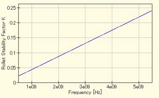
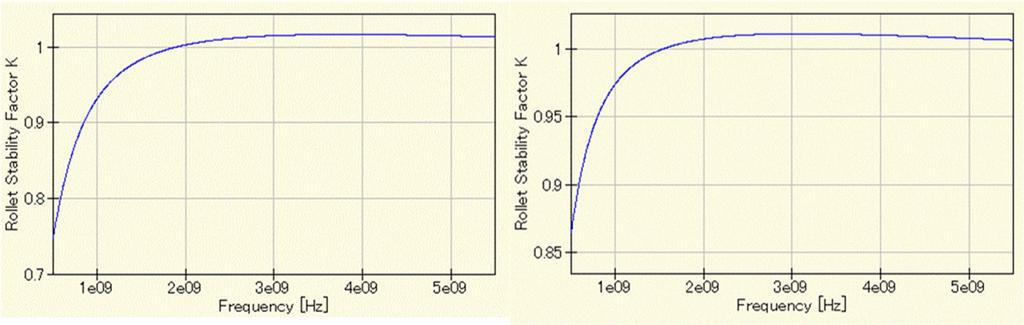
18 Rollet Stability (K) Factor Unconditionally Stable When K>1 K 1 S S22 S 2 S S S S 12 S 21 2
 -0.5 Finding Target Point -1.")
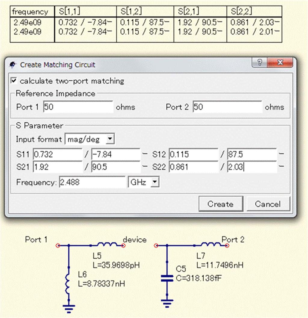
19 Matching Circuit Design Using Smith Chart Stability Circle S12S21 S 1 S 22 S Constant G Plot 2 Element (2) Element (1) 5 10 (2) Design Point Constant NF Circle -0.2 S 11 S (1) -0.5 Finding Target Point -1.0 Designing Input Matching Circuit Designing Output Matching Circuit Verification (Often S 11 and S 22 are NOT acceptable -2 Gain and NF are Dependent on Bias Current (Voltage)
20 Power Efficiency of Class A Amplifier V cc V L e in V L V cc V cc /2 1 R L 1 R 1 T L T 0 1 T V cc T V sin(2t / T ) dt 2 o V 2 cc V o sin(2t / T ) dt Maximum 25% (at V o =V cc /2) V V o cc t
21 Power Efficiency of Class B Amplifier +V cc V L +V cc V L e in 0 1 R 1 R L L 2 T 2 T T 0 T / 2 0 / 2 V V cc o o -V cc t -V cc Output sin(2t / T ) V 2 dt sin(2t / T ) dt Maximum 78.5% (at V o =V cc ) V 4 V o cc 0 Class B Class A Input
22 V DS V DD t Efficiency Distortion Class A max =50% for RF I D t Class B max =78.5% I D t Class C max =100% (At P=0) I D t Good Bad
23 Power Amplifier DC Cut Capacitor RF Choke Rejecting RF Leakage V DD L 2 e in L 1 C 1 M 1 C 2 C 1 R eout L Harmonics Suppression V b Z Matching + Z Conversion e in V DD L D M 1 M 2 V DD L D R L Driver + Main Amplifier V b
24 Linear High Efficiency PA Pre-distortion Feedback Compensation Waveform Generation Power Amp. Detector Memory Effect (Hysteresis) Problem Feed-Forward PA Power Amp. Delay ATT Delay + - Amplifier Error Detection and Compensation + -
25 Linear Amplifier with Non-linear Components (LINC) E( t) A( t)sin( t ( t)) A 2 max where (t)=cos -1 (A(t)/A max ) c [cos( t ( t) ( t)) cos( t ( t) ( t))] c Constant Amplitude c Non-Linear PA Applicable Waveform Generation PA-1 PA-2 + -
26 Contents Noise Figures and Non-Linearities RF Amplifiers Low Noise Amplifier Design Example


27 Use of High Speed Transistor BFP620 Design Low Noise Amplifier at GHz. V cc =1.5 V and I c =5 ma. Low NF and Return Suppression Mandatory. How High Gain Achievable?

28 Step 1 Bias Circuit Design

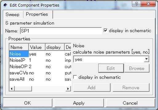
29 Step 2 S Parameter Simulation Caution!

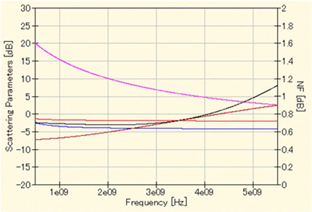
30 S Simulation Result S 21 NF S 11 NF min S 22 NF min : Achievable minimum NF at the given frequency

31 Impact of Emitter Degeneration Inductor
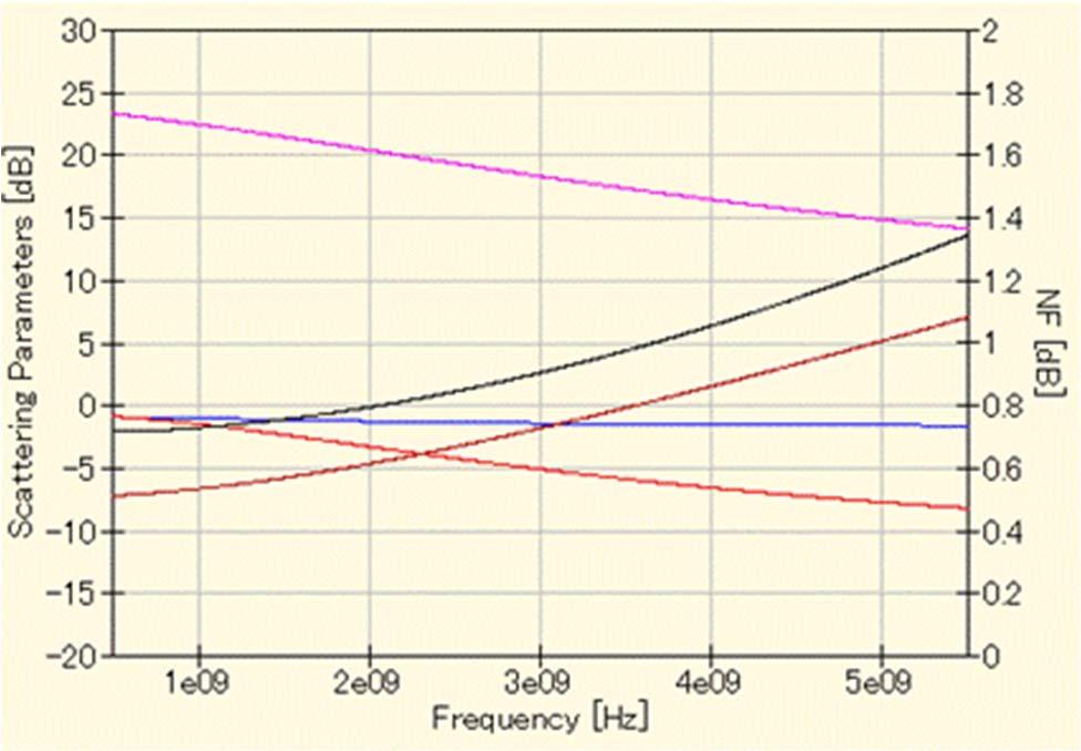


32 Simulation Results L=0 nh L=1 nh L=2 nh L=3 nh

33 Simulation Results L=0 nh L=1 nh L=2 nh L=3 nh

34 Step 3 Design Matching Circuits
35 Procedure

36 After Adding Designed Matching Circuit

37 Simulated Results S 11 and S 22 Suppression Astable?

38 Step 4 Stabilization Z Increase Z Increase Q Reduction

39 Simulation Results Stabilized

40 Step 5 Transient Analysis


41 Simulation Results Pin=-10 dbm Pin=-5 dbm

42 Step 6 Two Tone Analysis
![Two Tone Test Result P 2ab [dbm]=2 P a [dbm] + P b [dbm] - 2](/docs-images/87/96606129/images/43-0.jpg "OIP3 [dbm] -40.1=2 (-4.39) + (-4.5) - 2 OIP3 OIP3 =13.")
43 Two Tone Test Result P 2ab [dbm]=2 P a [dbm] + P b [dbm] - 2 OIP3 [dbm] -40.1=2 (-4.39) + (-4.5) - 2 OIP3 OIP3 =13.4 [dbm]
Application Note No. 158
 Application Note, Rev. 1.2, February 2008 Application Note No. 158 The BFP420 Transistor as a Low-Cost 900 MHz ISM Band Power Amplifier RF & Protection Devices Edition 2008-02-27 Published by Infineon
CHAPTER 3 CMOS LOW NOISE AMPLIFIERS
 46 CHAPTER 3 CMOS LOW NOISE AMPLIFIERS 3.1 INTRODUCTION The Low Noise Amplifier (LNA) plays an important role in the receiver design. LNA serves as the first block in the RF receiver. It is a critical
Application Note No. 149
 Application Note, Rev. 1.2, February 2008 1.8 V, 2.6 ma Low Noise Amplifier for 1575 MHz GPS L1 Frequency with the BFP405 RF Transistor Small Signal Discretes Edition 2008-02-22 Published by Infineon Technologies
50 MHz to 4.0 GHz RF/IF Gain Block ADL5602
 Data Sheet FEATURES Fixed gain of 20 db Operation from 50 MHz to 4.0 GHz Highest dynamic range gain block Input/output internally matched to 50 Ω Integrated bias control circuit OIP3 of 42.0 dbm at 2.0
SmartSpice RF Harmonic Balance Based RF Simulator. Advanced RF Circuit Simulation
 SmartSpice RF Harmonic Balance Based RF Simulator Advanced RF Circuit Simulation SmartSpice RF Overview Uses harmonic balance approach to solve system equations in frequency domain Well suited for RF and
Low voltage LNA, mixer and VCO 1GHz
 DESCRIPTION The is a combined RF amplifier, VCO with tracking bandpass filter and mixer designed for high-performance low-power communication systems from 800-1200MHz. The low-noise preamplifier has a
Application Note No. 124
 Application Note, Rev. 1.2, September 2007 Low Noise Amplifier for 2.3 to 2.5 GHz Applications using the SiGe BFP640F Tranistor Small Signal Discretes Edition 2007-09-06 Published by Infineon Technologies
SmartSpice RF Harmonic Balance Based and Shooting Method Based RF Simulation
 SmartSpice RF Harmonic Balance Based and Shooting Method Based RF Simulation Silvaco Overview SSRF Attributes Harmonic balance approach to solve system of equations in frequency domain Well suited for
RFIC DESIGN ELEN 351 Session4
 RFIC DESIGN ELEN 351 Session4 Dr. Allen Sweet January 29, 2003 Copy right 2003 ELEN 351 1 Power Amplifier Classes Indicate Efficiency and Linearity Class A: Most linear, max efficiency is 50% Class AB:
1 of 7 12/20/ :04 PM
 1 of 7 12/20/2007 11:04 PM Trusted Resource for the Working RF Engineer [ C o m p o n e n t s ] Build An E-pHEMT Low-Noise Amplifier Although often associated with power amplifiers, E-pHEMT devices are
1GHz low voltage LNA, mixer and VCO
 DESCRIPTION The is a combined RF amplifier, VCO with tracking bandpass filter and mixer designed for high-performance low-power communication systems from 800-1200MHz. The low-noise preamplifier has a
IF Digitally Controlled Variable-Gain Amplifier
 19-2601; Rev 1; 2/04 IF Digitally Controlled Variable-Gain Amplifier General Description The high-performance, digitally controlled variable-gain amplifier is designed for use from 0MHz to 400MHz. The
ADI 2006 RF Seminar. Chapter II RF/IF Components and Specifications for Receivers
 ADI 2006 RF Seminar Chapter II RF/IF Components and Specifications for Receivers 1 RF/IF Components and Specifications for Receivers Fixed Gain and Variable Gain Amplifiers IQ Demodulators Analog-to-Digital
Introduction to CMOS RF Integrated Circuits Design
 VII. ower Amplifiers VII-1 Outline Functionality Figures of Merit A Design Classical Design (Class A, B, C) High-Efficiency Design (Class E, F) Matching Network Linearity T/R Switches VII-2 As and TRs
915 MHz Power Amplifier. EE172 Final Project. Michael Bella
 915 MHz Power Amplifier EE17 Final Project Michael Bella Spring 011 Introduction: Radio Frequency Power amplifiers are used in a wide range of applications, and are an integral part of many daily tasks.
30 MHz to 6 GHz RF/IF Gain Block ADL5544
 Data Sheet FEATURES Fixed gain of 17.4 db Broadband operation from 3 MHz to 6 GHz Input/output internally matched to Ω Integrated bias control circuit OIP3 of 34.9 dbm at 9 MHz P1dB of 17.6 dbm at 9 MHz
RF2334. Typical Applications. Final PA for Low Power Applications Broadband Test Equipment
 RF233 AMPLIFIER Typical Applications Broadband, Low Noise Gain Blocks IF or RF Buffer Amplifiers Driver Stage for Power Amplifiers Final PA for Low Power Applications Broadband Test Equipment Product Description
Application Note 5057
 A 1 MHz to MHz Low Noise Feedback Amplifier using ATF-4143 Application Note 7 Introduction In the last few years the leading technology in the area of low noise amplifier design has been gallium arsenide
SGA-6489 SGA-6489Z Pb
 Product Description The SGA-689 is a high performance SiGe HBT MMIC Amplifier. A Darlington configuration featuring micron emitters provides high F T and excellent thermal perfomance. The heterojunction
RF, Microwave & Wireless. All rights reserved
 RF, Microwave & Wireless All rights reserved 1 Non-Linearity Phenomenon All rights reserved 2 Physical causes of nonlinearity Operation under finite power-supply voltages Essential non-linear characteristics
SGA7489Z DC to 3000MHz SILICON GERMANIUM HBT CASCADABLE GAIN BLOCK
 DC to 3MHz Silicon Germanium HBT Cascadable Gain Block SGA7489Z DC to 3MHz SILICON GERMANIUM HBT CASCADABLE GAIN BLOCK Package: SOT-89 Product Description The SGA7489Z is a high performance SiGe HBT MMIC
Application Note 5303
 MGA-6P8 9 MHz low noise amplifier using MGA-6P8 Application Note 5 Introduction The MGA-6P8 is a GaAs EPHEMT with an integrated active bias. The target applications are Tower Mounted Amplifier / Main LNA
Low-Voltage IF Transceiver with Limiter/RSSI and Quadrature Modulator
 19-1296; Rev 2; 1/1 EVALUATION KIT MANUAL FOLLOWS DATA SHEET Low-Voltage IF Transceiver with General Description The is a highly integrated IF transceiver for digital wireless applications. It operates
TLCE - A3 08/09/ /09/ TLCE - A DDC. IF channel Zc. - Low noise, wide dynamic Ie Vo 08/09/ TLCE - A DDC
 Politecnico di Torino ICT School Telecommunication Electronics A3 Amplifiers nonlinearity» Reference circuit» Nonlinear models» Effects of nonlinearity» Applications of nonlinearity Large signal amplifiers
30 MHz to 6 GHz RF/IF Gain Block ADL5611
 Data Sheet FEATURES Fixed gain of 22.2 db Broad operation from 3 MHz to 6 GHz High dynamic range gain block Input and output internally matched to Ω Integrated bias circuit OIP3 of 4. dbm at 9 MHz P1dB
Application Note No. 027
 Application Note, Rev. 2.0, Jan. 2007 Application Note No. 027 Using the BGA420 Si MMIC Amplifier for Various UHF Applications from 300 MHz to 2.5 GHz RF & Protection Devices Edition 2007-01-11 Published
ATF-531P8 E-pHEMT GaAs FET Low Noise Amplifier Design for 800 and 900 MHz Applications. Application Note 1371
 ATF-31P8 E-pHEMT GaAs FET Low Noise Amplifier Design for 8 and 9 MHz Applications Application Note 1371 Introduction A critical first step in any LNA design is the selection of the active device. Low cost
30 MHz to 6 GHz RF/IF Gain Block ADL5610
 Data Sheet FEATURES Fixed gain of 18.4 db Broad operation from 3 MHz to 6 GHz High dynamic range gain block Input and output internally matched to Ω Integrated bias circuit OIP3 of 38.8 dbm at 9 MHz P1dB
RF3376 General Purpose Amplifier
 General Purpose Amplifier RF3376 General Purpose Amplifier Package Style: SOT8 Features DC to >6000MHz Operation Internally Matched Input and Output 22dB Small Signal Gain +2.0dB Noise Figure +11dBm Output
MD3880DB1: Ultrasound Low Noise Amplifier Demoboard
 MD388DB1: Ultrasound Low Noise Amplifier Demoboard MD388DB1 General Description The MD388DB1 demoboard is a platform for testing and evaluating the MD388 4-channel low-noise amplifi er (LNA) with a variable
1 MHz to 2.7 GHz RF Gain Block AD8354
 1 MHz to 2.7 GHz RF Gain Block AD834 FEATURES Fixed gain of 2 db Operational frequency of 1 MHz to 2.7 GHz Linear output power up to 4 dbm Input/output internally matched to Ω Temperature and power supply
1 MHz to 2.7 GHz RF Gain Block AD8354
 Data Sheet FEATURES Fixed gain of 2 db Operational frequency of 1 MHz to 2.7 GHz Linear output power up to 4 dbm Input/output internally matched to Ω Temperature and power supply stable Noise figure: 4.2
GPS/GNSS Front-End Amplifier
 EVALUATION KIT AVAILABLE MAX2678 General Description The MAX2678 GPS/GNSS front-end amplifier IC is designed for automotive and marine GPS/GNSS satellite navigation antenna modules, or for any application
Low noise amplifier, principles
 1 Low noise amplifier, principles l l Low noise amplifier (LNA) design Introduction -port noise theory, review LNA gain/noise desense Bias network and its effect on LNA IP3 LNA stability References Why
T he noise figure of a
 LNA esign Uses Series Feedback to Achieve Simultaneous Low Input VSWR and Low Noise By ale. Henkes Sony PMCA T he noise figure of a single stage transistor amplifier is a function of the impedance applied
400 MHz to 4000 MHz ½ Watt RF Driver Amplifier ADL5324
 Data Sheet FEATURES Operation from MHz to MHz Gain of 14.6 db at 21 MHz OIP of 4.1 dbm at 21 MHz P1dB of 29.1 dbm at 21 MHz Noise figure of.8 db Dynamically adjustable bias Adjustable power supply bias:.
TOP VIEW IF LNAIN IF IF LO LO
 -3; Rev ; / EVALUATION KIT AVAILABLE Low-Cost RF Up/Downconverter General Description The performs the RF front-end transmit/ receive function in time-division-duplex (TDD) communication systems. It operates
SA620 Low voltage LNA, mixer and VCO 1GHz
 INTEGRATED CIRCUITS Low voltage LNA, mixer and VCO 1GHz Supersedes data of 1993 Dec 15 2004 Dec 14 DESCRIPTION The is a combined RF amplifier, VCO with tracking bandpass filter and mixer designed for high-performance
Application Note 5295
 MGA-63P8 1.9 GHz low noise amplifier using MGA-63P8 Application Note 595 Introduction The MGA-63P8 is a GaAs EPHEMT with an integrated active bias. The target applications are Tower Mounted Amplifier /
MGA-632P8 1.9 GHz low noise amplifier Application Note 5295
 MGA-63P8 1.9 GHz low noise amplifier Application Note 595 Introduction The MGA-63P8 is a GaAs EPHEMT LNA with integrated active bias. The target applications are Tower Mounted Amplifiers and LNAs in cellular
QUICK START GUIDE FOR DEMONSTRATION CIRCUIT 678A 40MHZ TO 900MHZ DIRECT CONVERSION QUADRATURE DEMODULATOR
 DESCRIPTION QUICK START GUIDE FOR DEMONSTRATION CIRCUIT 678A LT5517 Demonstration circuit 678A is a 40MHz to 900MHz Direct Conversion Quadrature Demodulator featuring the LT5517. The LT 5517 is a direct
Application Note 5460
 MGA-89 High Linearity Amplifier with Low Operating Current for 9 MHz to. GHz Applications Application Note 6 Introduction The Avago MGA-89 is a high dynamic range amplifier designed for applications in
Designing an LNA for a CDMA front end
 signal processing Designing an LNA for a CDMA front end LNA design is critical in modern communication systems. Understanding necessary additional design considerations can save both time and money. The
RF2317. Laser Diode Driver Return Channel Amplifier Base Stations. CATV Distribution Amplifiers Cable Modems Broadband Gain Blocks
 CATV Distribution Amplifiers Cable Modems Broadband Gain Blocks Laser Diode Driver Return Channel Amplifier Base Stations The is a general purpose, low cost high linearity RF amplifier IC. The device is
Gain and Return Loss vs Frequency. s22. Frequency (GHz)
") SBA4086Z DCto5GHz, CASCADABLE InGaP/GaAs HBT MMIC AMPLIFIER Package: SOT-86 Product Description RFMD s SBA4086Z is a high performance InGaP/GaAs Heterojunction Bipolar Transistor MMIC Amplifier. A Darlington
SBA4086Z DCto5GHz, CASCADABLE InGaP/GaAs HBT MMIC AMPLIFIER Package: SOT-86 Product Description RFMD s SBA4086Z is a high performance InGaP/GaAs Heterojunction Bipolar Transistor MMIC Amplifier. A Darlington
Application Note 1285
 Low Noise Amplifiers for 5.125-5.325 GHz and 5.725-5.825 GHz Using the ATF-55143 Low Noise PHEMT Application Note 1285 Description This application note describes two low noise amplifiers for use in the
RADIO RECEIVERS ECE 3103 WIRELESS COMMUNICATION SYSTEMS
 RADIO RECEIVERS ECE 3103 WIRELESS COMMUNICATION SYSTEMS FUNCTIONS OF A RADIO RECEIVER The main functions of a radio receiver are: 1. To intercept the RF signal by using the receiver antenna 2. Select the
NOT FOR NEW DESIGNS SGA5386Z. Absolute Maximum Ratings MHz. Parameter Rating Unit. Typical Performance at Key Operating Frequencies
 DC to 5MHz, Cascadable SiGe HBT MMIC Amplifier DC to 5MHz, CASCADABLE SiGe HBT MMIC AMPLIFIER Package: SOT-86 Product Description The is a high performance SiGe HBT MMIC Amplifier. A Darlington configuration
Application Note 1373
 ATF-511P8 900 MHz High Linearity Amplifier Application Note 1373 Introduction Avago s ATF-511P8 is an enhancement mode PHEMT designed for high linearity and medium power applications. With an OIP3 of 41
A Low Noise Amplifier with HF Selectivity
 A Low Noise Amplifier with HF Selectivity Johan Karlsson Mikael Grudd Radio project 2008 Department of Electrical and Information Technology Lund University Supervisor: Göran Jönsson Abstract This report
Code: 9A Answer any FIVE questions All questions carry equal marks *****
 II B. Tech II Semester (R09) Regular & Supplementary Examinations, April/May 2012 ELECTRONIC CIRCUIT ANALYSIS (Common to EIE, E. Con. E & ECE) Time: 3 hours Max Marks: 70 Answer any FIVE questions All
W-CDMA Upconverter and PA Driver with Power Control
 19-2108; Rev 1; 8/03 EVALUATION KIT AVAILABLE W-CDMA Upconverter and PA Driver General Description The upconverter and PA driver IC is designed for emerging ARIB (Japan) and ETSI-UMTS (Europe) W-CDMA applications.
Driver Amplifier for 7 Tesla MRI Smart Power Amplifier
 Driver Amplifier for 7 Tesla MRI Smart Power Amplifier presented by Kevin Kolpatzeck supervised by Prof. Dr.-Ing. Klaus Solbach Institute of Microwave and RF Technology University of Duisburg Essen Contents
RF3375 GENERAL PURPOSE AMPLIFIER
 Basestation Applications Broadband, Low-Noise Gain Blocks IF or RF Buffer Amplifiers Driver Stage for Power Amplifiers Final PA for Low-Power Applications High Reliability Applications RF3375General Purpose
CHAPTER 4 ULTRA WIDE BAND LOW NOISE AMPLIFIER DESIGN
 93 CHAPTER 4 ULTRA WIDE BAND LOW NOISE AMPLIFIER DESIGN 4.1 INTRODUCTION Ultra Wide Band (UWB) system is capable of transmitting data over a wide spectrum of frequency bands with low power and high data
RF V LOW NOISE AMPLIFIER/ 3V DRIVER AMPLIFIER
 3.3V LOW NOISE AMPLIFIER/ 3V DRIVER AMPLIFIER Package Style: SOT 5-Lead Features Low Noise and High Intercept Point Adjustable Bias Current Power Down Control Single 2.7V to 5.0V Power Supply 0.4GHz to
A GSM Band Low-Power LNA 1. LNA Schematic
 A GSM Band Low-Power LNA 1. LNA Schematic Fig1.1 Schematic of the Designed LNA 2. Design Summary Specification Required Simulation Results Peak S21 (Gain) > 10dB >11 db 3dB Bandwidth > 200MHz (
A 3-Stage Shunt-Feedback Op-Amp having 19.2dB Gain, 54.1dBm OIP3 (2GHz), and 252 OIP3/P DC Ratio
, and 252 OIP3/P DC Ratio") International Microwave Symposium 2011 Chart 1 A 3-Stage Shunt-Feedback Op-Amp having 19.2dB Gain, 54.1dBm OIP3 (2GHz), and 252 OIP3/P DC Ratio Zach Griffith, M. Urteaga, R. Pierson, P. Rowell, M. Rodwell,
International Microwave Symposium 2011 Chart 1 A 3-Stage Shunt-Feedback Op-Amp having 19.2dB Gain, 54.1dBm OIP3 (2GHz), and 252 OIP3/P DC Ratio Zach Griffith, M. Urteaga, R. Pierson, P. Rowell, M. Rodwell,
Title: New High Efficiency Intermodulation Cancellation Technique for Single Stage Amplifiers.
 Title: New High Efficiency Intermodulation Cancellation Technique for Single Stage Amplifiers. By: Ray Gutierrez Micronda LLC email: ray@micronda.com February 12, 2008. Introduction: This article provides
ATF High Intercept Low Noise Amplifier for the MHz PCS Band using the Enhancement Mode PHEMT
 ATF-54143 High Intercept Low Noise Amplifier for the 185 191 MHz PCS Band using the Enhancement Mode PHEMT Application Note 1222 Introduction Avago Technologies ATF-54143 is a low noise enhancement mode
ELEN 701 RF & Microwave Systems Engineering. Lecture 8 November 8, 2006 Dr. Michael Thorburn Santa Clara University
 ELEN 701 RF & Microwave Systems Engineering Lecture 8 November 8, 2006 Dr. Michael Thorburn Santa Clara University System Noise Figure Signal S1 Noise N1 GAIN = G Signal G x S1 Noise G x (N1+No) Self Noise
RF/IF Terminology and Specs
 RF/IF Terminology and Specs Contributors: Brad Brannon John Greichen Leo McHugh Eamon Nash Eberhard Brunner 1 Terminology LNA - Low-Noise Amplifier. A specialized amplifier to boost the very small received
The Design of A 125W L-Band GaN Power Amplifier
 Sheet Code RFi0613 White Paper The Design of A 125W L-Band GaN Power Amplifier This paper describes the design and evaluation of a single stage 125W L-Band GaN Power Amplifier using a low-cost packaged
Evaluating and Optimizing Tradeoffs in CMOS RFIC Upconversion Mixer Design. by Dr. Stephen Long University of California, Santa Barbara
 Evaluating and Optimizing Tradeoffs in CMOS RFIC Upconversion Mixer Design by Dr. Stephen Long University of California, Santa Barbara It is not easy to design an RFIC mixer. Different, sometimes conflicting,
SGA2386ZDC to 5000MHz, Cascadable. SiGe HBT. MMIC Amplifier. Frequency (GHz) 2800 MHz >10dB 97 C/W
 2800 MHz >10dB 97 C/W") DC to 5MHz, Cascadable SiGe HBT MMIC Amplifier DC to 5MHz, CASCADABLE SiGe HBT MMIC AMPLIFIER Package: SOT-86 Product Description The is a high performance SiGe HBT MMIC Amplifier. A Darlington configuration
DC to 5MHz, Cascadable SiGe HBT MMIC Amplifier DC to 5MHz, CASCADABLE SiGe HBT MMIC AMPLIFIER Package: SOT-86 Product Description The is a high performance SiGe HBT MMIC Amplifier. A Darlington configuration
Triple/Dual-Mode CDMA LNA/Mixers
 19-17; Rev 2; 4/3 EVALUATION KIT AVAILABLE Triple/Dual-Mode CDMA LNA/Mixers General Description The receiver RF front-end IC is designed for dual-band CDMA cellular phones and can also be used in dual-band
Measuring 3rd order Intercept Point (IP3 / TOI) of an amplifier
 of an amplifier") Measuring 3rd order Intercept Point (IP3 / TOI) of an amplifier Why measuring IP3 / TOI? IP3 is an important parameter for nonlinear systems like mixers or amplifiers which helps to verify the quality
Measuring 3rd order Intercept Point (IP3 / TOI) of an amplifier Why measuring IP3 / TOI? IP3 is an important parameter for nonlinear systems like mixers or amplifiers which helps to verify the quality
Design and Layout of a X-Band MMIC Power Amplifier in a Phemt Technology
 Design and Layout of a X-Band MMIC Power Amplifier in a Phemt Technology Renbin Dai, and Rana Arslan Ali Khan Abstract The design of Class A and Class AB 2-stage X band Power Amplifier is described in
High Gain Low Noise Amplifier Design Using Active Feedback
 Chapter 6 High Gain Low Noise Amplifier Design Using Active Feedback In the previous two chapters, we have used passive feedback such as capacitor and inductor as feedback. This chapter deals with the
DISCRETE SEMICONDUCTORS DATA SHEET. book, halfpage MBD128. BGA2709 MMIC wideband amplifier. Preliminary specification 2002 Jan 31
 DISCRETE SEMICONDUCTORS DATA SHEET book, halfpage MBD128 22 Jan 31 FEATURES Internally matched to 5 Ω Very wide frequency range (3.6 GHz at 3 db bandwidth) Flat 23 db gain (DC to 2.6 GHz at 1 db flatness)
14 MHz Single Side Band Receiver
 EPFL - LEG Laboratoires à options 8 ème semestre MHz Single Side Band Receiver. Objectives. The objective of this work is to calculate and adjust the key elements of an Upper Side Band Receiver in the
LF to 4 GHz High Linearity Y-Mixer ADL5350
 LF to GHz High Linearity Y-Mixer ADL535 FEATURES Broadband radio frequency (RF), intermediate frequency (IF), and local oscillator (LO) ports Conversion loss:. db Noise figure:.5 db High input IP3: 25
Case Study: Amp5. Design of a WiMAX Power Amplifier. WiMAX power amplifier. Amplifier topology. Power. Amplifier
 MICROWAVE AND DESIGN Case Study: Amp5 Design of a WiMAX Presented by Michael Steer Reading: Chapter 19, Section 19.6 Index: CS_Amp5 Based on material in Microwave and Design: A Systems Approach, nd Edition,
High Intercept Low Noise Amplifier for 1.9 GHz PCS and 2.1 GHz W-CDMA Applications using the ATF Enhancement Mode PHEMT
 High Intercept Low Noise Amplifier for 1.9 GHz PCS and 2.1 GHz W-CDMA Applications using the ATF-55143 Enhancement Mode PHEMT Application Note 1241 Introduction Avago Technologies ATF-55143 is a low noise
MCP to 2.5 GHz RF Front End IC. Description
 Description The contains a power amplifier (PA), a low noise amplifier (LNA), and two SPDT switch. It is a 0-pins IC by 4 4mm -QFN package. RF input and output impedance of are 50Ω matched. Therefore,
ATF-531P8 900 MHz High Linearity Amplifier. Application Note 1372
 ATF-531P8 9 MHz High Linearity Amplifier Application Note 1372 Introduction This application note describes the design and construction of a single stage 85 MHz to 9 MHz High Linearity Amplifier using
GHz LOW NOISE AMPLIFIER WHM AE 1
 .. GHz LOW NOISE AMPLIFIER WHM-AE WHM-AE LNA is a low noise figure, wideband, and high linearity SMT packaged amplifier. The amplifier offers typical noise figure of.9 db and output IP of. dbm at the frequency
RF9986. Micro-Cell PCS Base Stations Portable Battery Powered Equipment
 RF996 CDMA/TDMA/DCS900 PCS Systems PHS 500/WLAN 2400 Systems General Purpose Down Converter Micro-Cell PCS Base Stations Portable Battery Powered Equipment The RF996 is a monolithic integrated receiver
An All CMOS, 2.4 GHz, Fully Adaptive, Scalable, Frequency Hopped Transceiver
 An All CMOS, 2.4 GHz, Fully Adaptive, Scalable, Frequency Hopped Transceiver Farbod Behbahani John Leete Alexandre Kral Shahrzad Tadjpour Karapet Khanoyan Paul J. Chang Hooman Darabi Maryam Rofougaran
SC5307A/SC5308A 100 khz to 6 GHz RF Downconverter. Datasheet SignalCore, Inc.
 SC5307A/SC5308A 100 khz to 6 GHz RF Downconverter Datasheet 2017 SignalCore, Inc. support@signalcore.com P RODUCT S PECIFICATIONS Definition of Terms The following terms are used throughout this datasheet
BIPOLAR ANALOG INTEGRATED CIRCUITS PC2709TB
 DATA SHEET BIPOLAR ANALOG INTEGRATED CIRCUITS PC279TB 5 V, SUPER MINIMOLD SILICON MMIC MEDIUM OUTPUT POWER AMPLIFIER DESCRIPTION The PC279TB is asilicon monolithic integrated circuits designed as 1st IF
ESD Sensitive Component!!
 5 MHz LOW NOISE AMPLIFIER WHM3AE 1 REV E WHM3AE LNA is a low noise figure, wideband, and high linear SMT packaged amplifier with exceptional gain flatness design. The amplifier offers typical.7 db noise
6.976 High Speed Communication Circuits and Systems Lecture 8 Noise Figure, Impact of Amplifier Nonlinearities
 6.976 High Speed Communication Circuits and Systems Lecture 8 Noise Figure, Impact of Amplifier Nonlinearities Michael Perrott Massachusetts Institute of Technology Copyright 2003 by Michael H. Perrott
MAX2387/MAX2388/MAX2389
 19-13; Rev 1; /1 EVALUATION KIT AVAILABLE W-CDMA LNA/Mixer ICs General Description The MAX37/MAX3/ low-noise amplifier (LNA), downconverter mixers designed for W-CDMA applications, are ideal for ARIB (Japan)
SGA4586Z DC to 4000MHz, CASCADABLE SiGe HBT MMIC AMPLIFIER
 DC to 4MHz, Cascadable SiGe HBT MMIC Amplifier DC to 4MHz, CASCADABLE SiGe HBT MMIC AMPLIFIER Package: SOT-86 Product Description The is a high performance SiGe HBT MMIC Amplifier. A Darlington configuration
Data Sheet SC5317 & SC5318A. 6 GHz to 26.5 GHz RF Downconverter SignalCore, Inc. All Rights Reserved
 Data Sheet SC5317 & SC5318A 6 GHz to 26.5 GHz RF Downconverter www.signalcore.com 2018 SignalCore, Inc. All Rights Reserved Definition of Terms 1 Table of Contents 1. Definition of Terms... 2 2. Description...
MGA GHz 3 V, 17 dbm Amplifier. Data Sheet. Features. Description. Applications. Surface Mount Package. Simplified Schematic
 MGA-853.1 GHz 3 V, 17 dbm Amplifier Data Sheet Description Avago s MGA-853 is an economical, easy-to-use GaAs MMIC amplifier that offers excellent power and low noise figure for applications from.1 to
MAINTENANCE MANUAL TRANSMITTER/RECEIVER BOARD CMN-234A/B FOR MLSU141 & MLSU241 UHF MOBILE RADIO TABLE OF CONTENTS
 MAINTENANCE MANUAL TRANSMITTER/RECEIVER BOARD CMN-234A/B FOR MLSU141 & MLSU241 UHF MOBILE RADIO TABLE OF CONTENTS DESCRIPTION... 2 CIRCUIT ANALYSIS... 2 TRANSMITTER... 2 9-Voft Regulator... 2 Exciter...
Surface Mount SOT-363 (SC-70) Package. Pin Connections and Package Marking 4 V CC. Note: Package marking provides orientation and identification.
 Package. Pin Connections and Package Marking 4 V CC. Note: Package marking provides orientation and identification.") 1.5 GHz Low Noise Silicon MMIC Amplifier Technical Data INA-52063 Features Ultra-Miniature Package Single 5 V Supply (30 ma) 22 db Gain 8 dbm P 1dB Unconditionally Stable Applications Amplifier for Cellular,
1.5 GHz Low Noise Silicon MMIC Amplifier Technical Data INA-52063 Features Ultra-Miniature Package Single 5 V Supply (30 ma) 22 db Gain 8 dbm P 1dB Unconditionally Stable Applications Amplifier for Cellular,
CMY210. Demonstration Board Documentation / Applications Note (V1.0) Ultra linear General purpose up/down mixer 1. DESCRIPTION
 Ultra linear General purpose up/down mixer 1. DESCRIPTION") Demonstration Board Documentation / (V1.0) Ultra linear General purpose up/down mixer Features: Very High Input IP3 of 24 dbm typical Very Low LO Power demand of 0 dbm typical; Wide input range Wide LO
Demonstration Board Documentation / (V1.0) Ultra linear General purpose up/down mixer Features: Very High Input IP3 of 24 dbm typical Very Low LO Power demand of 0 dbm typical; Wide input range Wide LO
AT General Purpose, Low Current NPN Silicon Bipolar Transistor. Data Sheet
 AT-4532 General Purpose, Low Current NPN Silicon Bipolar Transistor Data Sheet Description Avago s AT-4532 is a general purpose NPN bipolar transistor that has been optimized for maximum f t at low voltage
1 Introduction RF receivers Transmission observation receiver Thesis Objectives Outline... 3
 Printed in Sweden E-huset, Lund, 2016 Abstract In this thesis work, a highly linear passive attenuator and mixer were designed to be used in a wide-band Transmission Observation Receiver (TOR). The TOR
TSEK02: Radio Electronics Lecture 8: RX Nonlinearity Issues, Demodulation. Ted Johansson, EKS, ISY
 TSEK02: Radio Electronics Lecture 8: RX Nonlinearity Issues, Demodulation Ted Johansson, EKS, ISY RX Nonlinearity Issues: 2.2, 2.4 Demodulation: not in the book 2 RX nonlinearities System Nonlinearity
AN increasing number of video and communication applications
 1470 IEEE JOURNAL OF SOLID-STATE CIRCUITS, VOL. 32, NO. 9, SEPTEMBER 1997 A Low-Power, High-Speed, Current-Feedback Op-Amp with a Novel Class AB High Current Output Stage Jim Bales Abstract A complementary
30 MHz to 6 GHz RF/IF Gain Block ADL5611
 Preliminary Technical Data FEATURES Fixed gain of 22.1 db Broad operation from 30 MHz to 6 GHz High dynamic range gain block Input/output internally matched to 50 Ω Integrated bias control circuit OIP3
KH103 Fast Settling, High Current Wideband Op Amp
 KH103 Fast Settling, High Current Wideband Op Amp Features 80MHz full-power bandwidth (20V pp, 100Ω) 200mA output current 0.4% settling in 10ns 6000V/µs slew rate 4ns rise and fall times (20V) Direct replacement
Efficiency (%) Characteristic Symbol Min Typ Max Units
 Characteristic Symbol Min Typ Max Units") PTF181 LDMOS RF Power Field Effect Transistor W, 185 188 MHz, 193 199 MHz W, 21 217 MHz Description Features The PTF181 is a W, internally matched GOLDMOS FET device intended for EDGE applications in the
PTF181 LDMOS RF Power Field Effect Transistor W, 185 188 MHz, 193 199 MHz W, 21 217 MHz Description Features The PTF181 is a W, internally matched GOLDMOS FET device intended for EDGE applications in the
Application Note 1360
 ADA-4743 +17 dbm P1dB Avago Darlington Amplifier Application Note 1360 Description Avago Technologies Darlington Amplifier, ADA-4743 is a low current silicon gain block RFIC amplifier housed in a 4-lead
Application Note 1299
 A Low Noise High Intercept Point Amplifier for 9 MHz Applications using ATF-54143 PHEMT Application Note 1299 1. Introduction The Avago Technologies ATF-54143 is a low noise enhancement mode PHEMT designed
DISCONTINUED PC3232TB BIPOLAR ANALOG INTEGRATED CIRCUIT 5 V, SILICON GERMANIUM MMIC MEDIUM OUTPUT POWER AMPLIFIER DESCRIPTION FEATURES APPLICATIONS
 DESCRIPTION BIPOLAR ANALOG INTEGRATED CIRCUIT PC3232TB 5 V, SILICON GERMANIUM MMIC MEDIUM OUTPUT POWER AMPLIFIER The PC3232TB is a silicon germanium (SiGe) monolithic integrated circuit designed as IF