LME V Audio Power Amplifier Driver with Baker Clamp
|
|
|
- Hugh Rose
- 5 years ago
- Views:
Transcription

1 200V Audio Power Amplifier Driver with Baker Clamp General Description The LME49810 is a high fidelity audio power amplifier driver designed for demanding consumer and pro-audio applications. Amplifier output power may be scaled by changing the supply voltage and number of power transistors. The LME49810 s minimum output current is 50mA. When using a discrete output stage the LME49810 is capable of delivering in excess of 300 watts into a single-ended 8Ω load. Unique to the LME49810 is an internal Baker Clamp. This clamp insures that the amplifier output does not saturate when over driven. The resultant soft clipping of high level audio signals suppresses undesirable audio artifacts generated when conventional solid state amplifiers are driven hard into clipping. The LME49810 includes thermal shutdown circuitry that activates when the die temperature exceeds 150 C. The LME49810 s mute function, when activated, mutes the input drive signal and forces the amplifier output to a quiescent state. Key Specifications May 2007 Wide operating voltage range ±20V to ±100V Slew Rate Output Drive Current PSRR (f = DC) THD+N (f = 1kHz) Features Very high voltage operation Output clamp logic output Thermal shutdown and mute Customizable external compensation Scalable output power Applications Guitar amplifiers Powered studio monitors Powered subwoofers Pro audio Audio video receivers High voltage industrial applications 50V/μs (typ) 60mA (typ) 110dB (typ) (typ) LME V Audio Power Amplifier Driver with Baker Clamp Boomer is a registered trademark of National Semiconductor Corporation. Tru-GND is a trademark of National Semiconductor Corporation National Semiconductor Corporation
2 Typical Application FIGURE 1. LME49810 Audio Amplifier Schematic 2
3 Connection Diagram TB Package LME49810 Top View Order Number LME49810TB See NS Package Number TB15A N = National Logo U = Fabrication plant code Z = Assembly plant code XY = 2 Digit date code TT = Die traceability TB = Package code Pin Descriptions Pin Pin Name Description 1 ClpFlag Baker Clamp Clip Flag Output 2 Mute Mute Control 3 GND Device Ground 4 IN+ Non-Inverting Input 5 IN Inverting Input 6 Comp External Compensation Connection 7 NC No Connect, Pin electrically isolated 8 Osense Output Sense 9 NC No Connect, Pin electrically isolated 10 V EE Negative Power Supply 11 Bias M Negative External Bias Control 12 Bias P Positive External Bias Control 13 Sink Output Sink 14 Source Output Source 15 +V CC Positive Power Supply 3
4 FIGURE 2. LME49810 Simplified Schematic 4
5 Absolute Maximum Ratings (Notes 1, 2) If Military/Aerospace specified devices are required, please contact the National Semiconductor Sales Office/ Distributors for availability and specifications. Supply Voltage V + + V - 200V Differential Input Voltage ±6V Common Mode Input Range 0.4V EE to 0.4V CC Power Dissipation (Note 3) 4W ESD Susceptibility (Note 4) 1kV ESD Susceptibility (Note 5) 200V Junction Temperature (T JMAX ) (Note 9) 150 C Soldering Information T Package (10 seconds) 260 C Storage Temperature 40 C to +150 C Thermal Resistance θ JA θ JC Operating Ratings Temperature Range 73 C/W 4 C/W T MIN T A T MAX 40 C T A +8 5 C Supply Voltage ±20V V SUPPLY ±100V LME49810 Electrical Characteristics V CC = +100V, V EE = 100V (Notes 1, 2) The following specifications apply for I MUTE = 100μA, unless otherwise specified. Limits apply for T A = 25 C, C C = 10pF, and A V = 29dB. Symbol Parameter Conditions Typical (Note 6) LME49810 Limits (Notes 7, 8) Units (Limits) I CC Quiescent Power Supply Current V CM = 0V, V O = 0V, I O = 0A ma (max) I EE Quiescent Power Supply Current V CM = 0V, V O = 0V, I O = 0A 13 ma (max) THD+N Total Harmonic Distortion + Noise A V Open Loop Gain No Load, BW = 30kHz V OUT = 30V RMS, f = 1kHz f = DC f = 1kHz, V IN = 1mV RMS % (max) V OM Output Voltage Swing THD+N = 0.05%, f = 1kHz 67.5 V RMS V NOISE Output Noise BW = 30kHz, A-weighted db db μv μv (max) I OUT Output Current Current from Source to Sink Pins ma (min) I MUTE Current into Mute Pin To activate the amplifier 100 SR Slew Rate V IN = 1V P-P, f = 10kHz square Wave μa (min) μa (max) 50 V/μs(min) V OS Input Offset Voltage V CM = 0V, I O = 0mA 1 3 mv (max) I B Input Bias Current V CM = 0V, I O = 0mA na (max) PSRR Power Supply Rejection Ratio f = DC, Input Referred db (min) V CLIP Baker Clamp Clipping Voltage Clip Output Source pin Sink pin V BC Baker Clamp Flag Output Voltage I FLAG = 4.7mA 0.4 V V BA Bias P&M Pin Open Voltage BiasP - BiasM 10 V I BIAS Bias Adjust Function Current 2.8 ma V (max) V (min) 5
6 Note 1: All voltages are measured with respect to the GND pin unless otherwise specified. Note 2: Absolute Maximum Ratings indicate limits beyond which damage to the device may occur. Operating Ratings indicate conditions for which the device is functional but do not guarantee specific performance limits. Electrical Characteristics state DC and AC electrical specifications under particular test conditions which guarantee specific performance limits. This assumes that the device is within the Operating Ratings. Specifications are not guaranteed for parameters where no limit is given, however, the typical value is a good indication of device performance. Note 3: The maximum power dissipation must be derated at elevated temperatures and is dictated by T JMAX, θ JC, and the ambient temperature, T A. The maximum allowable power dissipation is P DMAX = (T JMAX - T A ) / θ JC or the number given in Absolute Maximum Ratings, whichever is lower. For the LME49810, T JMAX = 150 C and the typical θ JC is 4 C/W. Refer to the Thermal Considerations section for more information. Note 4: Human body model, 100pF discharged through a 1.5kΩ resistor. Note 5: Machine Model, 220pF - 240pF discharged through all pins. Note 6: Typicals are measured at +25 C and represent the parametric norm. Note 7: Limits are guaranteed to National's AOQL (Average Outgoing Quality Level). Note 8: Datasheet min/max specification limits are guaranteed by design, test, or statistical analysis. Note 9: The maximum operating junction temperature is 150 C. Note 10: Data taken with Bandwidth = 30kHz, A V = 29dB, C C = 10pF, and T A = 25 C except where specified. 6
7 FIGURE 3. LME49810 Test Circuit Schematic (DC Coupled) 7


8 Typical Performance Characteristics (Note 10) THD+N vs Frequency +V CC = V EE = 20V, V O = 5V THD+N vs Frequency +V CC = V EE = 20V, V O = 10V THD+N vs Frequency +V CC = V EE = 50V, V O = 14V THD+N vs Frequency +V CC = V EE = 50V, V O = 20V THD+N vs Frequency +V CC = V EE = 100V, V O = 14V THD+N vs Frequency +V CC = V EE = 50V, V O = 30V


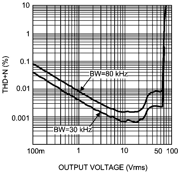
9 THD+N vs Output Voltage +V CC = V EE = 50V, f = 20Hz THD+N vs Output Voltage +V CC = V EE = 100V, f = 20Hz LME THD+N vs Output Voltage +V CC = V EE = 50V, f = 1kHz THD+N vs Output Voltage +V CC = V EE = 100V, f = 1kHz THD+N vs Output Voltage +V CC = V EE = 50V, f = 20kHz THD+N vs Output Voltage +V CC = V EE = 100V, f = 20kHz

10 THD+N vs Output Voltage +V CC = V EE = 20V, f = 20Hz THD+N vs Output Voltage +V CC = V EE = 20V, f = 1kHz THD+N vs Output Voltage +V CC = V EE = 20V, f = 20kHz Closed Loop Frequency Response +V CC = V EE = 50V, V IN = 1V RMS Closed Loop Frequency Response +V CC = V EE = 100V, V IN = 1V RMS PSRR vs Frequency +V CC = V EE = 100V, No Filters, Input referred, V RIPPLE = 1V RMS on V CC pin
11 PSRR vs Frequency +V CC = V EE = 100V, No Filters, Input referred, V RIPPLE = 1V RMS on V EE pin Mute Attenuation vs I MUTE +V CC = V EE = 100V LME Output Voltage vs Supply Voltage Slew Rate vs Compensation Capacitor +V CC = V EE = 100V, V IN = 1.2V P 10kHz squarewave Supply Current vs Supply Voltage Input Offset Voltage vs Supply Voltage


12 Open Loop Gain and Phase Margin +V CC = V EE = 100V CMRR vs Frequency +V CC = V EE = 100V Noise Floor +V CC = V EE = 50V, V IN = 0V Noise Floor +V CC = V EE = 100V, V IN = 0V Baker Clamp Flag Output +V CC = V EE = 100V, V IN = 4V RMS, f IN = 20kHz Ch1: Output, Ch2: CLPFLAG Output
13 Application Information MUTE FUNCTION The mute function of the LME49810 is controlled by the amount of current that flows into the MUTE pin. LME49810 typically requires 50μA to 100μA of mute current flowing in order to be in play mode. This can be done by connecting a reference voltage (V MUTE ) to the MUTE pin through a resistor (R M ). The following formula can be used to calculate the mute current. I MUTE = (V MUTE -0.7V) / (R M +10kΩ) (A) (1) reference voltage is not available, the following circuit using a Zener diode can be used to power the CLPFLAG pin from the higher supply voltage rails of the LME The power dissipation rating of R Z will need to be at-least ½W if using a 5V Zener Diode. Alternately, the following basic formula can be used to find the proper power rating of R Z : P DZ = (V CC - V Z ) 2 /R Z (W). This formula can also be used to meet the design requirements of any other reference voltage that the user desires. LME49810 The 10kΩ resistor value in Equation 1 is internal. Please refer to Figure 2, LME49810 Simplified Schematic, for additional details. For example, if a 5V voltage is connected through a 33kΩ resistor to the MUTE pin, then the mute current will be 100μA, according to Equation 1. Consequently, R M can be changed to suit any other reference voltage requirement. The LME49810 will enter Mute mode if I MUTE is less than 1μA which can be accomplished by shorting the MUTE pin to ground or by floating the MUTE pin. It is not recommended that more than 200μA flow into the MUTE pin because damage to LME49810 may occur and device may not function properly. BAKER CLAMP AND CLAMP FLAG OUTPUT The LME49810 features a Baker Clamp function with corresponding CLPFLAG output pin. The clamp function keeps all transistors in linear operation when the output goes into clipping. In addition, when the output goes into clipping, a logic low level appears at the CLPFLAG pin. The CLPFLGAG pin can be used to drive an LED or some other visual display as shown by Figure 1. The value of logic low voltage varies and depends on I FLAG. For example, if I FLAG is 4.7mA then a voltage (V BC ) of 0.4V will appear at the CLPFLAG output pin. The smooth response of the Baker Clamp and the corresponding CLPFLAG logic output is shown in the scope photo below: V CC = -V EE = 100V, V IN = 4V RMS, f IN = 1kHz, R C = 1kΩ Ch1: Output, Ch2: CLPFLAG Output The CLPFLAG pin can source up to 10mA, and since the CLPFLAG output is an open collector output as shown by Figure 2, LME49810 Simplified Schematic, it should never be left to float under normal operation. If CLPFLAG pin is not used, then it should be connected through a resistor to a reference voltage so that I FLAG is below 10mA. For example, a resistor of 1k can be used with a 5V reference voltage. This will give the I FLAG of 4.7mA. In a typical LED setup, if +5V THERMAL PROTECTION The LME49810 has a thermal protection scheme to prevent long-term thermal stress of the device. When the temperature on the die exceeds 150 C, the LME49810 goes into thermal shutdown. The LME49810 starts operating again when the die temperature drops to about 145 C, but if the temperature again begins to rise, shutdown will occur again above 150 C. Therefore, the device is allowed to heat up to a relatively high temperature if the fault condition is temporary, but a sustained fault will cause the device to cycle between the thermal shutdown temperature limits of 150 C and 145 C. This greatly reduces the stress imposed on the IC by thermal cycling, which in turn improves its reliability under sustained fault conditions. Since the die temperature is directly dependent upon the heat sink used, the heat sink should be chosen so that thermal shutdown is not activated during normal operation. Using the best heat sink possible within the cost and space constraints of the system will improve the long-term reliability of any power semiconductor device, as discussed in the Determining the Correct Heat Sink section. POWER DISSIPATION When in play mode, the LME49810 draws a constant amount of current, regardless of the input signal amplitude. Consequently, the power dissipation is constant for a given supply voltage and can be computed with the equation P DMAX = I CC * (V CC V EE ). For a quick calculation of P DMAX, approximate the current to be 11mA and multiply it by the total supply voltage (the current varies slightly from this value over the operating range). DETERMINING THE CORRECT HEAT SINK The choice of a heat sink for a high-power audio amplifier is made entirely to keep the die temperature at a level such that the thermal protection circuitry is not activated under normal circumstances. The thermal resistance from the die to the outside air, θ JA (junction to ambient), is a combination of three thermal resistances, θ JC (junction to case), θ CS (case to sink), and θ SA (sink to ambient). The thermal resistance, θ JC (junction to case), of the LME49810 is 4 C/W. Using Thermalloy Thermacote thermal compound, the thermal resistance, θ CS (case to sink), is about 0.2 C/W. Since convection heat flow (power dissipation) is analogous to current flow, thermal resistance is analogous to electrical resistance, and temperature drops are 13
14 analogous to voltage drops, the power dissipation out of the LME49810 is equal to the following: P DMAX = (T JMAX T AMB ) / θ JA (2) where T JMAX = 150 C, T AMB is the system ambient temperature and θ JA = θ JC + θ CS + θ SA Once the maximum package power dissipation has been calculated using Equation 2, the maximum thermal resistance, θ SA, (heat sink to ambient) in C/W for a heat sink can be calculated. This calculation is made using Equation 3 which is derived by solving for θ SA from Equation 2. θ SA = [(T JMAX T AMB ) P DMAX (θ JC +θ CS )] / P DMAX (3) Again it must be noted that the value of θ SA is dependent upon the system designer's amplifier requirements. If the ambient temperature that the audio amplifier is to be working under is higher than 25 C, then the thermal resistance for the heat sink, given all other things are equal, will need to be smaller. PROPER SELECTION OF EXTERNAL COMPONENTS Proper selection of external components is required to meet the design targets of an application. The choice of external component values that will affect gain and low frequency response are discussed below. The overall gain of the amplifier is set by resistors R F and R i for the non-inverting configuration shown in Figure 1. The gain is found by Equation 4 below given R i = R IN and R F = R S. A V = R F / R i (V/V) (4) For best Noise performance, lower values of resistors are used. A value of 243 is commonly used for R i and setting the value for R F for desired gain. For the LME49810 the gain should be set no lower than 10V/V. Gain settings below 10V/ V may experience instability. The combination of R i and C i (see Figure 1) creates a high pass filter. The gain at low frequency and therefore the response is determined by these components. The -3dB point can be determined from Equation 5 shown below: f i = 1 / (2πR i C i ) (Hz) (5) If an input coupling capacitor (C IN ) is used to block DC from the inputs as shown in Figure 1, there will be another high pass filter created with the combination of C IN and R IN. The resulting -3dB frequency response due to the combination of C IN and R IN can be found from equation 6 shown below: f IN = 1 / (2πR IN C IN ) (Hz) (6) For best audio performance, the input capacitor should not be used. Without the input capacitor, any DC bias from the source will be transferred to the load. The feedback capacitor (C i ) is used to set the gain at DC to unity. Because a large value is required for a low frequency -3dB point, the capacitor is an electrolytic type. An additional small value, high quality film capacitor may be used in parallel with the feedback resistor to improve high frequency sonic performance. If DC offset in the output stage is acceptable without the feedback capacitor, it may be removed but DC gain will now be equal to AC gain. COMPENSATION CAPACITOR The compensation capacitor (C C ) is one of the most critical external components in value, placement and type. The capacitor should be placed close to the LME49810 and a silver mica type will give good performance. The value of the capacitor will affect slew rate and stability. The highest slew rate is possible while also maintaining stability through out the power and frequency range of operation results in the best audio performance. The value shown in Figure 1 should be considered a starting value with optimization done on the bench and in listening testing. Please refer to Slew Rate vs. C C Graph in Typical Performance Characteristics for determining the proper slew rate for your particular application. SUPPLY BYPASSING The LME49810 has excellent power supply rejection and does not require a regulated supply. However, to eliminate possible oscillations all op amps and power op amps should have their supply leads bypassed with low-inductance capacitors having short leads and located close to the package terminals. Inadequate power supply bypassing will manifest itself by a low frequency oscillation known as motorboating or by high frequency instabilities. These instabilities can be eliminated through multiple bypassing utilizing a large electrolytic capacitor (10μF or larger) which is used to absorb low frequency variations and a small ceramic capacitor (0.1μF) to prevent any high frequency feedback through the power supply lines. If adequate bypassing is not provided the current in the supply leads which is a rectified component of the load current may be fed back into internal circuitry. This signal causes low distortion at high frequencies requiring that the supplies be bypassed at the package terminals with an electrolytic capacitor of 470μF or more. OUTPUT STAGE USING BIPOLAR TRANSISTORS With a properly designed output stage and supply voltage of ±100V, an output power up to 500W can be generated at 0.05% THD+N into an 8Ω speaker load. With an output current of several amperes, the output transistors need substantial base current drive because power transistors usually have quite low current gain typical h fe of 50 or so. To increase the current gain, audio amplifiers commonly use Darlington style devices. Power transistors should be mounted together with the V BE multiplier transistor on the same heat sink to avoid thermal run away. Please see the section Biasing Technique and Avoiding Thermal Runaway for additional information. BIASING TECHNIQUES AND AVOIDING THERMAL RUNAWAY A class AB amplifier has some amount of distortion called Crossover distortion. To effectively minimize the crossover distortion from the output, a V BE multiplier may be used instead of two biasing diodes. The LME49810 has two dedicated pins (BIAS M and BIAS P ) for Bias setup and provide a constant current source of about 2.8mA. A V BE multiplier normally consists of a bipolar transistor (Q MULT, see Figure 1) and two resistors (R B1 and R B2, see Figure 1). A trim pot can also be added in series with R B1 for optional bias adjustment. A properly designed output stage, combine with a V BE multiplier, 14
15 can eliminate the trim pot and virtually eliminate crossover distortion. The V CE voltage of Q MULT (also called BIAS of the output stage) can be set by following formula: V BIAS = V BE (1+R B2 /R B1 ) (V) (7) When using a bipolar output stage with the LME49810 (as in Figure 1), the designer must beware of thermal runaway. Thermal runaway is a result of the temperature dependence of V BE (an inherent property of the transistor). As temperature increases, V BE decreases. In practice, current flowing through a bipolar transistor heats up the transistor, which lowers the V BE. This in turn increases the current gain, and the cycle repeats. If the system is not designed properly this positive feedback mechanism can destroy the bipolar transistors used in the output stage. One of the recommended methods of preventing thermal runaway is to use the same heat sink on the bipolar output stage transistor together with V BE multiplier transistor. When the V BE multiplier transistor is mounted to the same heat sink as the bipolar output stage transistors, it temperature will track that of the output transistors. Its V BE is dependent upon temperature as well, and so it will draw more current as the output transistors heat up, reducing the bias voltage to compensate. This will limit the base current into the output transistors, which counteracts thermal runaway. Another widely popular method of preventing thermal runaway is to use low value emitter degeneration resistors (R E1 and R E2 ). As current increases, the voltage at the emitter also increases, which decreases the voltage across the base and emitter. This mechanism helps to limit the current and counteracts thermal runaway. LAYOUT CONSIDERATION AND AVOIDING GROUND LOOPS A proper layout is virtually essential for a high performance audio amplifier. It is very important to return the load ground, supply grounds of output transistors, and the low level (feedback and input) grounds to the circuit board common ground point through separate paths. When ground is routed in this fashion, it is called a star ground or a single point ground. It is advisable to keep the supply decoupling capacitors of 0.1μF close as possible to LME49810 to reduce the effects of PCB trace resistance and inductance. Following the general rules will optimize the PCB layout and avoid ground loops problems: a) Make use of symmetrical placement of components. b) Make high current traces, such as output path traces, as wide as possible to accomodate output stage current requirement. c) To reduce the PCB trace resistance and inductance, same ground returns paths should be as short as possible. If possible, make the output traces short and equal in length. d) To reduce the PCB trace resistance and inductance, ground returns paths should be as short as possible. e) If possible, star ground or a single point ground should be observed. Advanced planning before starting the PCB can improve audio performance. LME
16 Demo Board Schematic FIGURE 4. LME49810 Test demo board schematic 16

17 Demonstration Board Layout LME49810 Silkscreen Layer Top Layer
18 Bottom Layer
19 Revision History Rev Date Description /24/07 Initial WEB release /29/07 Few text edits. LME
20 Physical Dimensions inches (millimeters) unless otherwise noted TO Lead Package Order Number LME49810TB NS Package Number TB15A 20
21 Notes LME

22 200V Audio Power Amplifier Driver with Baker Clamp Notes THE CONTENTS OF THIS DOCUMENT ARE PROVIDED IN CONNECTION WITH NATIONAL SEMICONDUCTOR CORPORATION ( NATIONAL ) PRODUCTS. NATIONAL MAKES NO REPRESENTATIONS OR WARRANTIES WITH RESPECT TO THE ACCURACY OR COMPLETENESS OF THE CONTENTS OF THIS PUBLICATION AND RESERVES THE RIGHT TO MAKE CHANGES TO SPECIFICATIONS AND PRODUCT DESCRIPTIONS AT ANY TIME WITHOUT NOTICE. NO LICENSE, WHETHER EXPRESS, IMPLIED, ARISING BY ESTOPPEL OR OTHERWISE, TO ANY INTELLECTUAL PROPERTY RIGHTS IS GRANTED BY THIS DOCUMENT. TESTING AND OTHER QUALITY CONTROLS ARE USED TO THE EXTENT NATIONAL DEEMS NECESSARY TO SUPPORT NATIONAL S PRODUCT WARRANTY. EXCEPT WHERE MANDATED BY GOVERNMENT REQUIREMENTS, TESTING OF ALL PARAMETERS OF EACH PRODUCT IS NOT NECESSARILY PERFORMED. NATIONAL ASSUMES NO LIABILITY FOR APPLICATIONS ASSISTANCE OR BUYER PRODUCT DESIGN. BUYERS ARE RESPONSIBLE FOR THEIR PRODUCTS AND APPLICATIONS USING NATIONAL COMPONENTS. PRIOR TO USING OR DISTRIBUTING ANY PRODUCTS THAT INCLUDE NATIONAL COMPONENTS, BUYERS SHOULD PROVIDE ADEQUATE DESIGN, TESTING AND OPERATING SAFEGUARDS. EXCEPT AS PROVIDED IN NATIONAL S TERMS AND CONDITIONS OF SALE FOR SUCH PRODUCTS, NATIONAL ASSUMES NO LIABILITY WHATSOEVER, AND NATIONAL DISCLAIMS ANY EXPRESS OR IMPLIED WARRANTY RELATING TO THE SALE AND/OR USE OF NATIONAL PRODUCTS INCLUDING LIABILITY OR WARRANTIES RELATING TO FITNESS FOR A PARTICULAR PURPOSE, MERCHANTABILITY, OR INFRINGEMENT OF ANY PATENT, COPYRIGHT OR OTHER INTELLECTUAL PROPERTY RIGHT. LIFE SUPPORT POLICY NATIONAL S PRODUCTS ARE NOT AUTHORIZED FOR USE AS CRITICAL COMPONENTS IN LIFE SUPPORT DEVICES OR SYSTEMS WITHOUT THE EXPRESS PRIOR WRITTEN APPROVAL OF THE CHIEF EXECUTIVE OFFICER AND GENERAL COUNSEL OF NATIONAL SEMICONDUCTOR CORPORATION. As used herein: Life support devices or systems are devices which (a) are intended for surgical implant into the body, or (b) support or sustain life and whose failure to perform when properly used in accordance with instructions for use provided in the labeling can be reasonably expected to result in a significant injury to the user. A critical component is any component in a life support device or system whose failure to perform can be reasonably expected to cause the failure of the life support device or system or to affect its safety or effectiveness. National Semiconductor and the National Semiconductor logo are registered trademarks of National Semiconductor Corporation. All other brand or product names may be trademarks or registered trademarks of their respective holders. Copyright 2007 National Semiconductor Corporation For the most current product information visit us at National Semiconductor Americas Customer Support Center new.feedback@nsc.com Tel: National Semiconductor Europe Customer Support Center Fax: +49 (0) europe.support@nsc.com Deutsch Tel: +49 (0) English Tel: +49 (0) Français Tel: +33 (0) National Semiconductor Asia Pacific Customer Support Center ap.support@nsc.com National Semiconductor Japan Customer Support Center Fax: jpn.feedback@nsc.com Tel:
LME49811 Audio Power Amplifier Series High Fidelity 200 Volt Power Amplifier Input Stage with Shutdown
 January 4, 2008 LME49811 Audio Power Amplifier Series High Fidelity 200 Volt Power Amplifier Input Stage with Shutdown General Description The LME49811 is a high fidelity audio power amplifier input stage
LM4702 Audio Power Amplifier Series Stereo High Fidelity 200 Volt Driver with Mute
 LM4702 Audio Power Amplifier Series Stereo High Fidelity 200 Volt Driver with Mute General Description The LM4702 is a high fidelity audio power amplifier driver designed for demanding consumer and pro-audio
LM675 Power Operational Amplifier
 Power Operational Amplifier General Description The LM675 is a monolithic power operational amplifier featuring wide bandwidth and low input offset voltage, making it equally suitable for AC and DC applications.
LM675 Power Operational Amplifier
 LM675 Power Operational Amplifier General Description The LM675 is a monolithic power operational amplifier featuring wide bandwidth and low input offset voltage, making it equally suitable for AC and
LME49710 High Performance, High Fidelity Audio Operational Amplifier
 High Performance, High Fidelity Audio Operational Amplifier General Description The LME49710 is part of the ultra-low distortion, low noise, high slew rate operational amplifier series optimized and fully
LM4808 Dual 105 mw Headphone Amplifier
 Dual 105 mw Headphone Amplifier General Description The is a dual audio power amplifier capable of delivering 105 mw per channel of continuous average power into a16ωload with 0.1% (THD+N) from a 5V power
LM4562 Dual High Performance, High Fidelity Audio Operational Amplifier
 October 2007 Dual High Performance, High Fidelity Audio Operational Amplifier General Description The is part of the ultra-low distortion, low noise, high slew rate operational amplifier series optimized
LM4752 Stereo 11W Audio Power Amplifier
 LM4752 Stereo 11W Audio Power Amplifier General Description The LM4752 is a stereo audio amplifier capable of delivering 11W per channel of continuous average output power to a 4Ω load, or 7W per channel
LM48820 Ground-Referenced, Ultra Low Noise, Fixed Gain, 95mW Stereo Headphone Amplifier
 June 2007 Ground-Referenced, Ultra Low Noise, Fixed Gain, 95mW Stereo Headphone Amplifier General Description The is a ground referenced, fixed-gain audio power amplifier capable of delivering 95mW of
LM Watt Fully Differential Audio Power Amplifier With RF Suppression and Shutdown
 March 2007 1.25 Watt Fully Differential Audio Power Amplifier With RF Suppression and Shutdown General Description The is a fully differential audio power amplifier primarily designed for demanding applications
LM9022 Vacuum Fluorescent Display Filament Driver
 Vacuum Fluorescent Display Filament Driver General Description The LM9022 is a bridged power amplifier capable of delivering typically 2W of continuous average power into a 10Ω filament load when powered
LM3940 1A Low Dropout Regulator for 5V to 3.3V Conversion
 1A Low Dropout Regulator for 5V to 3.3V Conversion General Description The LM3940 is a 1A low dropout regulator designed to provide 3.3V from a 5V supply. The LM3940 is ideally suited for systems which
LM W High-Efficiency Mono BTL Audio Power Amplifier
 10W High-Efficiency Mono BTL Audio Power Amplifier General Description The LM4680 is a high efficiency switching audio power amplifier primarily designed for demanding applications in flat panel monitors
Features. Applications SOT-23-5
 135MHz, Low-Power SOT-23-5 Op Amp General Description The is a high-speed, unity-gain stable operational amplifier. It provides a gain-bandwidth product of 135MHz with a very low, 2.4mA supply current,
LM4562 Dual High Performance, High Fidelity Audio Operational Amplifier
 Dual High Performance, High Fidelity Audio Operational Amplifier General Description The is part of the ultra-low distortion, low noise, high slew rate operational amplifier series optimized and fully
LM6118/LM6218 Fast Settling Dual Operational Amplifiers
 Fast Settling Dual Operational Amplifiers General Description The LM6118/LM6218 are monolithic fast-settling unity-gain-compensated dual operational amplifiers with ±20 ma output drive capability. The
LM Watt Audio Power Amplifier with Fade-In and Fade-Out
 1.1 Watt Audio Power Amplifier with Fade-In and Fade-Out General Description The is an audio power amplifier primarily designed for demanding applications in mobile phones and other portable communication
LM W Audio Power Amplifier with Shutdown Mode
 1.1W Audio Power Amplifier with Shutdown Mode General Description The is a bridge-connected audio power amplifier capable of delivering 1.1W of continuous average power to an 8Ω load with 1% THD+N using
LM mw Audio Power Amplifier with Shutdown Mode
 LM4862 675 mw Audio Power Amplifier with Shutdown Mode General Description The LM4862 is a bridge-connected audio power amplifier capable of delivering typically 675 mw of continuous average power to an
 Distributed by: www.jameco.com 1-800-831-4242 The content and copyrights of the attached material are the property of its owner. LM148/LM248/LM348 Quad 741 Op Amps General Description The LM148 series
 Distributed by: www.jameco.com 1-800-831-4242 The content and copyrights of the attached material are the property of its owner. Stereo 11W Audio Power Amplifier General Description The is a stereo audio
TL082 Wide Bandwidth Dual JFET Input Operational Amplifier
 TL082 Wide Bandwidth Dual JFET Input Operational Amplifier General Description These devices are low cost, high speed, dual JFET input operational amplifiers with an internally trimmed input offset voltage
LM79XX Series 3-Terminal Negative Regulators
 3-Terminal Negative Regulators General Description The LM79XX series of 3-terminal regulators is available with fixed output voltages of 5V, 12V, and 15V. These devices need only one external component
LPV7215 Micropower, CMOS Input, RRIO, 1.8V, Push-Pull Output Comparator
 November 2006 LPV7215 Micropower, CMOS Input, RRIO, 1.8V, Push-Pull Output Comparator General Description The LPV7215 is an ultra low-power comparator with a typical power supply current of 580 na. It
LM384 5W Audio Power Amplifier
 5W Audio Power Amplifier General Description The LM384 is a power audio amplifier for consumer applications. In order to hold system cost to a minimum, gain is internally fixed at 34 db. A unique input
LF353 Wide Bandwidth Dual JFET Input Operational Amplifier
 LF353 Wide Bandwidth Dual JFET Input Operational Amplifier General Description These devices are low cost, high speed, dual JFET input operational amplifiers with an internally trimmed input offset voltage
LM4731 Stereo 25W Audio Power Amplifier with Mute and Standby Modes
 LM4731 Stereo 25W Audio Power Amplifier with Mute and Standby Modes General Description Key Specifications The LM4731 is a stereo audio amplifier capable of delivering typically 25W per channel of continuous
LM4906 1W, Bypass-Capacitor-less Audio Amplifier with Internal Selectable Gain
 1W, Bypass-Capacitor-less Audio Amplifier with Internal Selectable Gain General Description Key Specifications The is an audio power amplifier primarily designed for demanding applications in mobile phones
LM384 5W Audio Power Amplifier
 5W Audio Power Amplifier General Description The LM384 is a power audio amplifier for consumer applications. In order to hold system cost to a minimum, gain is internally fixed at 34 db. A unique input
TL082 Wide Bandwidth Dual JFET Input Operational Amplifier
 TL082 Wide Bandwidth Dual JFET Input Operational Amplifier General Description These devices are low cost, high speed, dual JFET input operational amplifiers with an internally trimmed input offset voltage
LM837 Low Noise Quad Operational Amplifier
 LM837 Low Noise Quad Operational Amplifier General Description The LM837 is a quad operational amplifier designed for low noise, high speed and wide bandwidth performance. It has a new type of output stage
LM386 Low Voltage Audio Power Amplifier
 Low Voltage Audio Power Amplifier General Description The is a power amplifier designed for use in low voltage consumer applications. The gain is internally set to 20 to keep external part count low, but
 Distributed by: www.jameco.com 1-800-831-4242 The content and copyrights of the attached material are the property of its owner. LM4862 675 mw Audio Power Amplifier with Shutdown Mode General Description
LP2902/LP324 Micropower Quad Operational Amplifier
 LP2902/LP324 Micropower Quad Operational Amplifier General Description The LP324 series consists of four independent, high gain internally compensated micropower operational amplifiers. These amplifiers
LM4811 Dual 105mW Headphone Amplifier with Digital Volume Control and Shutdown Mode
 LM4811 Dual 105mW Headphone Amplifier with Digital Volume Control and Shutdown Mode General Description Key Specifications The LM4811 is a dual audio power amplifier capable of delivering 105mW per channel
LF412 Low Offset, Low Drift Dual JFET Input Operational Amplifier
 LF412 Low Offset, Low Drift Dual JFET Input Operational Amplifier General Description These devices are low cost, high speed, JFET input operational amplifiers with very low input offset voltage and guaranteed
LF442 Dual Low Power JFET Input Operational Amplifier
 LF442 Dual Low Power JFET Input Operational Amplifier General Description The LF442 dual low power operational amplifiers provide many of the same AC characteristics as the industry standard LM1458 while
LM6142 and LM MHz Rail-to-Rail Input-Output Operational Amplifiers
 LM6142 and LM6144 17 MHz Rail-to-Rail Input-Output Operational Amplifiers General Description Using patent pending new circuit topologies, the LM6142/44 provides new levels of performance in applications
LM6172 Dual High Speed, Low Power, Low Distortion, Voltage Feedback Amplifiers
 LM6172 Dual High Speed, Low Power, Low Distortion, Voltage Feedback Amplifiers General Description The LM6172 is a dual high speed voltage feedback amplifier. It is unity-gain stable and provides excellent
LMC7101 Tiny Low Power Operational Amplifier with Rail-To-Rail Input and Output
 Tiny Low Power Operational Amplifier with Rail-To-Rail Input and Output General Description The LMC7101 is a high performance CMOS operational amplifier available in the space saving SOT 23-5 Tiny package.
LM mW at 3.3V Supply Audio Power Amplifier with Shutdown Mode
 265mW at 3.3V Supply Audio Power Amplifier with Shutdown Mode General Description The is a bridged audio power amplifier capable of delivering 265mW of continuous average power into an 8Ω load with 1%
LM6162/LM6262/LM6362 High Speed Operational Amplifier
 LM6162/LM6262/LM6362 High Speed Operational Amplifier General Description The LM6362 family of high-speed amplifiers exhibits an excellent speed-power product, delivering 300 V/µs and 100 MHz gain-bandwidth
LM4755 Stereo 11W Audio Power Amplifier with Mute
 LM4755 Stereo 11W Audio Power Amplifier with Mute General Description The LM4755 is a stereo audio amplifier capable of delivering 11W per channel of continuous average output power to a 4Ω load or 7W
 Distributed by: www.jameco.com 1-800-831-4242 The content and copyrights of the attached material are the property of its owner. LM1877 Dual Audio Power Amplifier General Description The LM1877 is a monolithic
LM146/LM346 Programmable Quad Operational Amplifiers
 LM146/LM346 Programmable Quad Operational Amplifiers General Description The LM146 series of quad op amps consists of four independent, high gain, internally compensated, low power, programmable amplifiers.
LMH6672 Dual, High Output Current, High Speed Op Amp
 LMH6672 Dual, High Output Current, High Speed Op Amp General Description The LMH6672 is a low cost, dual high speed op amp capable of driving signals to within 1V of the power supply rails. It features
LP2980-ADJ Micropower SOT, 50 ma Ultra Low-Dropout Adjustable Voltage Regulator
 Micropower SOT, 50 ma Ultra Low-Dropout Adjustable Voltage Regulator General Description The LP2980-ADJ is a 50 ma adjustable voltage regulator designed to provide ultra low dropout in battery powered
LM4766 Typical Application
 LM4766 Overture Audio Power Amplifier Series Dual 40W Audio Power Amplifier with Mute General Description Key Specifications The LM4766 is a stereo audio amplifier capable of delivering typically 40W per
LM W Audio Power Amplifier
 LM380 2.5W Audio Power Amplifier General Description The LM380 is a power audio amplifier for consumer applications. In order to hold system cost to a minimum, gain is internally fixed at 34 db. A unique
CLC440 High Speed, Low Power, Voltage Feedback Op Amp
 CLC440 High Speed, Low Power, Voltage Feedback Op Amp General Description The CLC440 is a wideband, low power, voltage feedback op amp that offers 750MHz unity-gain bandwidth, 1500V/µs slew rate, and 90mA
LM321 Low Power Single Op Amp
 Low Power Single Op Amp General Description The LM321 brings performance and economy to low power systems. With a high unity gain frequency and a guaranteed 0.4V/µs slew rate, the quiescent current is
LF411JAN Low Offset, Low Drift JFET Input Operational Amplifier
 LF411JAN Low Offset, Low Drift JFET Input Operational Amplifier General Description This device is a low cost, high speed, JFET input operational amplifier with very low input offset voltage and guaranteed
Op Amp Booster Designs
 Op Amp Booster Designs Although modern integrated circuit operational amplifiers ease linear circuit design, IC processing limits amplifier output power. Many applications, however, require substantially
LM4765 OvertureAudio Power Amplifier Series Dual 30W Audio Power Amplifier with Mute and Standby Modes
 LM4765 Overture Audio Power Amplifier Series Dual 30W Audio Power Amplifier with Mute and Standby Modes General Description The LM4765 is a stereo audio amplifier capable of delivering typically 30W per
LF444 Quad Low Power JFET Input Operational Amplifier
 LF444 Quad Low Power JFET Input Operational Amplifier General Description The LF444 quad low power operational amplifier provides many of the same AC characteristics as the industry standard LM148 while
 Distributed by: www.jameco.com 1-800-831-4242 The content and copyrights of the attached material are the property of its owner. LM392 Low Power Operational Amplifier/Voltage Comparator General Description
LM7301 Low Power, 4 MHz GBW, Rail-to-Rail Input-Output Operational Amplifier in TinyPak Package
 Low Power, 4 MHz GBW, Rail-to-Rail Input-Output Operational Amplifier in TinyPak Package General Description The LM7301 provides high performance in a wide range of applications. The LM7301 offers greater
LME LME49713 High Performance, High Fidelity Current Feedback
 High Performance, High Fidelity Current Feedback Audio Operational Amplifier General Description The is an ultra-low distortion, low noise, ultra high slew rate current feedback operational amplifier optimized
LM2940/LM2940C 1A Low Dropout Regulator
 1A Low Dropout Regulator General Description Typical Application January 2007 The LM2940/LM2940C positive voltage regulator features the ability to source 1A of output current with a dropout voltage of
Features. Applications SOT-23-5 (M5)
") 1.8V to 11V, 15µA, 25kHz GBW, Rail-to-Rail Input and Output Operational Amplifier General Description The is a low-power operational amplifier with railto-rail inputs and outputs. The device operates from
1.8V to 11V, 15µA, 25kHz GBW, Rail-to-Rail Input and Output Operational Amplifier General Description The is a low-power operational amplifier with railto-rail inputs and outputs. The device operates from
LM7171 Very High Speed, High Output Current, Voltage Feedback Amplifier
 LM7171 Very High Speed, High Output Current, Voltage Feedback Amplifier General Description Features The LM7171 is a high speed voltage feedback amplifier that has the slewing characteristic of a current
LM833 Dual Audio Operational Amplifier
 LM833 Dual Audio Operational Amplifier General Description The LM833 is a dual general purpose operational amplifier designed with particular emphasis on performance in audio systems. This dual amplifier
Dual 20W Audio Power Amplifier with Mute and Standby Modes
 LM1876 Overture Audio Power Amplifier Series Dual 20W Audio Power Amplifier with Mute and Standby Modes General Description The LM1876 is a stereo audio amplifier capable of delivering typically 20W per
LM4951 Wide Voltage Range 1.8 Watt Audio Amplifier
 LM4951 Wide Voltage Range 1.8 Watt Audio Amplifier General Description The LM4951 is an audio power amplifier primarily designed for demanding applications in Portable Handheld devices. It is capable of
LM833 Dual Audio Operational Amplifier
 LM833 Dual Audio Operational Amplifier General Description The LM833 is a dual general purpose operational amplifier designed with particular emphasis on performance in audio systems. This dual amplifier
 Distributed by: www.jameco.com 1-800-831-4242 The content and copyrights of the attached material are the property of its owner. LM138/LM338 5-Amp Adjustable Regulators General Description The LM138 series
LM4562 Dual High Performance, High Fidelity Audio Operational Amplifier
 Dual High Performance, High Fidelity Audio Operational Amplifier General Description The is part of the ultra-low distortion, low noise, high slew rate operational amplifier series optimized and fully
LM6164/LM6264/LM6364 High Speed Operational Amplifier
 LM6164/LM6264/LM6364 High Speed Operational Amplifier General Description The LM6164 family of high-speed amplifiers exhibits an excellent speed-power product in delivering 300V per µs and 175 MHz GBW
LM392/LM2924 Low Power Operational Amplifier/Voltage Comparator
 LM392/LM2924 Low Power Operational Amplifier/Voltage Comparator General Description The LM392 series consists of 2 independent building block circuits. One is a high gain, internally frequency compensated
 Distributed by: www.jameco.com 1-800-831-4242 The content and copyrights of the attached material are the property of its owner. LM4765 Overture Audio Power Amplifier Series Dual 30W Audio Power Amplifier
LME49830 Mono High Fidelity 200 Volt MOSFET Power Amplifier Input Stage with Mute
 January 24, 2008 Mono High Fidelity 200 Volt MOSFET Power Amplifier Input Stage with Mute General Description The is a high fidelity audio power amplifier input stage designed for demanding consumer and
LMV761/LMV762 Low Voltage, Precision Comparator with Push-Pull Output
 LMV761/LMV762 Low Voltage, Precision Comparator with Push-Pull Output General Description The LMV761/762 are precision comparators intended for applications requiring low noise and low input offset voltage.
LMV nsec, 2.7V to 5V Comparator with Rail-to Rail Output
 7 nsec, 2.7V to 5V Comparator with Rail-to Rail Output General Description The is a low-power, high-speed comparator with internal hysteresis. The operating voltage ranges from 2.7V to 5V with push/pull
LM V, Mono 85mW BTL Output, 14mW Stereo Headphone Audio Amplifier
 1.5V, Mono 85mW BTL Output, 14mW Stereo Headphone Audio Amplifier General Description The unity gain stable LM4919 is both a mono-btl audio power amplifier and a Single Ended (SE) stereo headphone amplifier.
LM117HV/LM317HV 3-Terminal Adjustable Regulator
 3-Terminal Adjustable Regulator General Description The LM117HV/LM317HV are adjustable 3-terminal positive voltage regulators capable of supplying in excess of 1.5A over a 1.2V to 57V output range. They
LF453 Wide-Bandwidth Dual JFET-Input Operational Amplifiers
 LF453 Wide-Bandwidth Dual JFET-Input Operational Amplifiers General Description The LF453 is a low-cost high-speed dual JFET-input operational amplifier with an internally trimmed input offset voltage
j Quiscent Power Supply Current j P OUT Features
 LM4952 3.1W Stereo-SE Audio Power Amplifier with DC Volume Control General Description The LM4952 is a dual audio power amplifier primarily designed for demanding applications in flat panel monitors and
LMP8100 Programmable Gain Amplifier
 Programmable Gain Amplifier General Description The programmable gain amplifier features an adjustable gain from 1 to 16 V/V in 1 V/V increments. At the core of the is a precision, 33 MHz, CMOS input,
LM2991 Negative Low Dropout Adjustable Regulator
 LM2991 Negative Low Dropout Adjustable Regulator General Description The LM2991 is a low dropout adjustable negative regulator with a output voltage range between 3V to 24V. The LM2991 provides up to 1A
LM6161/LM6261/LM6361 High Speed Operational Amplifier
 LM6161/LM6261/LM6361 High Speed Operational Amplifier General Description The LM6161 family of high-speed amplifiers exhibits an excellent speed-power product in delivering 300 V/µs and 50 MHz unity gain
LMS8117A 1A Low-Dropout Linear Regulator
 LMS8117A 1A Low-Dropout Linear Regulator General Description The LMS8117A is a series of low dropout voltage regulators with a dropout of 1.2V at 1A of load current. It has the same pin-out as National
LMV841 / LMV844 CMOS Input, RRIO, Wide Supply Range Operational Amplifiers
 LMV841 / LMV844 CMOS Input, RRIO, Wide Supply Range Operational Amplifiers General Description The LMV841 and LMV844 are low-voltage and low-power operational amplifiers that operate with supply voltages
Practical RTD Interface Solutions
 Practical RTD Interface Solutions 1.0 Purpose This application note is intended to review Resistance Temperature Devices and commonly used interfaces for them. In an industrial environment, longitudinal
LM150/LM350A/LM350 3-Amp Adjustable Regulators
 LM150/LM350A/LM350 3-Amp Adjustable Regulators General Description The LM150 series of adjustable 3-terminal positive voltage regulators is capable of supplying in excess of 3A over a 1.2V to 33V output
LM2682 Switched Capacitor Voltage Doubling Inverter
 Switched Capacitor Voltage Doubling Inverter General Description The LM2682 is a CMOS charge-pump voltage inverter capable of converting positive voltage in the range of +2.0V to +5.5V to the corresponding
LF451 Wide-Bandwidth JFET-Input Operational Amplifier
 LF451 Wide-Bandwidth JFET-Input Operational Amplifier General Description The LF451 is a low-cost high-speed JFET-input operational amplifier with an internally trimmed input offset voltage (BI- FET IITM
LM4860 Series 1W Audio Power Amplifier with Shutdown Mode
 Series 1W Audio Power Amplifier with Shutdown Mode General Description The LM4860 is a bridge-connected audio power amplifier capable of delivering 1W of continuous average power to an 8Ω load with less
LM118/LM218/LM318 Operational Amplifiers
 LM118/LM218/LM318 Operational Amplifiers General Description The LM118 series are precision high speed operational amplifiers designed for applications requiring wide bandwidth and high slew rate. They
LM133/LM333 3-Ampere Adjustable Negative Regulators
 LM133/LM333 3-Ampere Adjustable Negative Regulators General Description The LM133/LM333 are adjustable 3-terminal negative voltage regulators capable of supplying in excess of 3.0A over an output voltage
LP3470 Tiny Power On Reset Circuit
 Tiny Power On Reset Circuit General Description The LP3470 is a micropower CMOS voltage supervisory circuit designed to monitor power supplies in microprocessor (µp) and other digital systems. It provides
LM ma Low Dropout Regulator
 500 ma Low Dropout Regulator General Description July 2000 The LM2937 is a positive voltage regulator capable of supplying up to 500 ma of load current. The use of a PNP power transistor provides a low
Designing A SEPIC Converter
 Designing A SEPIC Converter Introduction In a SEPIC (Single Ended Primary Inductance Converter) design, the output voltage can be higher or lower than the input voltage. The SEPIC converter shown in Figure
LM4250 Programmable Operational Amplifier
 LM4250 Programmable Operational Amplifier General Description The LM4250 and LM4250C are extremely versatile programmable monolithic operational amplifiers. A single external master bias current setting
LM125 Precision Dual Tracking Regulator
 LM125 Precision Dual Tracking Regulator INTRODUCTION The LM125 is a precision, dual, tracking, monolithic voltage regulator. It provides separate positive and negative regulated outputs, thus simplifying
LM2412 Monolithic Triple 2.8 ns CRT Driver
 Monolithic Triple 2.8 ns CRT Driver General Description The is an integrated high voltage CRT driver circuit designed for use in high resolution color monitor applications. The IC contains three high input
 Distributed by: www.jameco.com 1-800-831-4242 The content and copyrights of the attached material are the property of its owner. LM78XX Series Voltage Regulators General Description Connection Diagrams
LM V Monolithic Triple Channel 15 MHz CRT DTV Driver
 220V Monolithic Triple Channel 15 MHz CRT DTV Driver General Description The is a triple channel high voltage CRT driver circuit designed for use in DTV applications. The IC contains three high input impedance,
DS80EP100 5 to 12.5 Gbps, Power-Saver Equalizer for Backplanes and Cables
 July 2007 5 to 12.5 Gbps, Power-Saver Equalizer for Backplanes and Cables General Description National s Power-saver equalizer compensates for transmission medium losses and minimizes medium-induced deterministic
Features. Applications
 Teeny Ultra-Low Power Op Amp General Description The is a rail-to-rail output, operational amplifier in Teeny SC70 packaging. The provides 4MHz gain-bandwidth product while consuming an incredibly low
 Distributed by: www.jameco.com 1-800-831-4242 The content and copyrights of the attached material are the property of its owner. LM137/LM337 3-Terminal Adjustable Negative Regulators General Description