UNIT I MICROWAVE NETWORK THEORY
|
|
|
- Felicity Morton
- 5 years ago
- Views:
Transcription
1 UNIT I MICROWAVE NETWORK THEORY Introduction Microwave frequency range, applications of microwaves Scattering matrix representation of multi port network properties of S-parameters S matrix of a two port network with mismatched load Z and ABCD parameters-comparison between [S] - [Z] and [Y] matrices
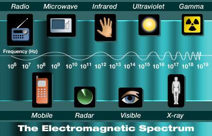
2 Electromagnetic spectrum
3 Microwaves Microwaves are electromagnetic waves whose frequencies range from about 300 MHz 300 GHz (1 MHz = 10 6 Hz and 1 GHz = 10 9 Hz) or wavelengths in air ranging from 100 cm 1 mm. The word Microwave means very short wave, which is the shortest wavelength region of the radio spectrum and a part of the electromagnetic spectrum.
4 Properties of Microwaves 1. Microwave is an electromagnetic radiation of short wavelength. 2. They can reflect by conducting surfaces just like optical waves since they travel in straight line. 3. Microwave currents flow through a thin outer layer of an ordinary cable. 4. Microwaves are easily attenuated within short distances. 5. They are not reflected by ionosphere
5
6 Applications Microwaves have a wide range of applications in modern technology, which are listed below 1. Telecommunication: Intercontinental Telephone and TV, space communication (Earth to space and space to Earth), telemetry communication link for railways etc. 2. Radars: detect aircraft, track / guide supersonic missiles, observe and track weather patterns, air traffic control (ATC), burglar alarms, garage door openers, police speed detectors etc.
7 Commercial and industrial applications Microwave oven Drying machines textile, food and paper industry for drying clothes, potato chips, printed matters etc. Food process industry Precooling / cooking, pasteurization / sterility, hat frozen / refrigerated precooled meats, roasting of food grains / beans. Rubber industry / plastics / chemical / forest product industries Mining / public works, breaking rocks, tunnel boring, drying / breaking up concrete, breaking up coal seams, curing of cement. Drying inks / drying textiles, drying / sterilizing grains, drying / sterilizing pharmaceuticals, leather, tobacco, power transmission. Biomedical Applications ( diagnostic / therapeutic ) diathermy for localized superficial heating, deep electromagnetic heating for treatment of cancer, hyperthermia ( local, regional or whole body for cancer therapy).
8 THE SCATTERING MATRIX Usually we use Y, Z, H or ABCD parameters to describe a linear two port network. These parameters require us to open or short a network to find the parameters. At radio frequencies it is difficult to have a proper short or open circuit, there are parasitic inductance and capacitance in most instances. Open/short condition leads to standing wave, can cause oscillation and destruction of device. For non-tem propagation mode, it is not possible to measure voltage and current. We can only measure power from E and H fields.
9 THE SCATTERING MATRIX Hence a new set of parameters (S) is needed which Do not need open/short condition. Do not cause standing wave. Relates to incident and reflected power waves, instead of voltage and current. As oppose to V and I, S-parameters relate the reflected and incident voltage waves. S-parameters have the following advantages: 1. Relates to familiar measurement such as reflection coefficient, gain, loss etc. 2. Can cascade S-parameters of multiple devices to predict system performance (similar to ABCD parameters). 3. Can compute Z, Y or H parameters from S-parameters if needed.
10 THE SCATTERING MATRIX Consider an n port network: Reference plane for local z-axis (z = 0) Z c1 Port 1 Each port is considered to be connected to a Tline with specific Z c. Port n Z cn Port 2 Z c2 Linear n - port network T-line or waveguide
11 THE SCATTERING MATRIX There is a voltage and current on each port. This voltage (or current) can be decomposed into the incident (+) and reflected component (-). V V z V 2 e jz V2 e jz 0 V 2 V 2 V2 z I I 2 e jz I2 e jz I 0 I2 I 2 I2 Port 2 V 1+ V 1 - Linear n - port Network Port 1 I 1 Port n V 1 z = 0 Port 1 +z + + V 1 V V - 1 V 1 V 1 V1 I 1 I 1 I1 1 V 1 V1 Zc1
12 THE SCATTERING MATRIX The port voltage and current can be normalized with respect to the impedance connected to it. It is customary to define normalized voltage waves at each port as: Normalized incident waves ai ai V i Zci I Z i ci (4.3a) i = 1, 2, 3 n V b i i Zci bi I Z i ci Normalized reflected waves (4.3b)
13 THE SCATTERING MATRIX Thus in general: V 1+ V 1 - Z c1 Port 1 V n + V n - Port n Port 2 V + 2 V - 2 Z c2 T-line or waveguide Linear n - port Network Z cn V i+ and V i- are propagating voltage waves, which can be the actual voltage for TEM modes or the equivalent voltages for non-tem modes. (for non-tem, V is defined proportional to transverse E field while I is defined proportional to transverse H field, see [1] for details).
14 THE SCATTERING MATRIX If the n port network is linear (make sure you know what this means!), there is a linear relationship between the normalized waves. For instance if we energize port 2: V 1 - Z c1 Port 1 V n - Port n V V s V s V V 2 + Port 2 Linear n - port Network Z cn V n s V n 2 2 V 2 - Z c2 Constant that depends on the network construction
15 THE SCATTERING MATRIX Considering that we can send energy into all ports, this can be generalized to: Or written in Matrix equation: Where sij is known as the generalized Scattering (S) parameter, or just S- parameters for short. From (4.3), each port i can have different characteristic impedance Zci n nn n n n n V s V s V s V s V (4.4a) (4.4b) or n s n V V s V s V s V n n V s V s V s V s V V S V n nn n n n n n V V V s s s s s s s s s V V V :... : : : :
16 THE SCATTERING MATRIX Consider the N-port network shown in figure 4.1. Figure 4.1: An arbitrary N-port microwave network
17 THE SCATTERING MATRIX V n+ is the amplitude of the voltage wave incident on port n. V n- is the amplitude of the voltage wave reflected from port n. The scattering matrix or [S] matrix, is defined in relation to these incident and reflected voltage wave as: n NN N N n V V V S S S S S S V V V [4.1a]
18 THE SCATTERING MATRIX or ij V S V A specific element of the [S] matrix can be determined as: S V V i j V k 0, for k j [4.1b] [4.2] S ij is found by driving port j with an incident wave V j+, and measuring the reflected wave amplitude, V i-, coming out of port i. The incident waves on all ports except j-th port are set to zero (which means that all ports should be terminated in matched load to avoid reflections). Thus, S ii is the reflection coefficient seen looking into port i when all other ports are terminated in matched loads, and S ij is the transmission coefficient from port j to port i when all other ports are terminated in matched loads.
19 THE SCATTERING MATRIX For 2-port networks, (4.4) reduces to: Note that V i+ = 0 implies that we terminate i th port with its characteristic impedance. Thus zero reflection eliminates standing wave V V S V V s s s s V V (4.5a) (4.5b) V V V V V V s V V s V V s V V s
20 THE SCATTERING MATRIX V + 1 V s Z c1 V 2 - Z c1 Z c2 2 Port Z c2 Measurement of s 11 and s 21 : V 1 - V 1 - s 11 V V 1 1 V 2 0 s 21 V V 2 1 V 2 0 V 2 + Z c2 V s Z c1 Z c1 2 Port Z c2 V 2 - Measurement of s 22 and s 12 : s 22 V V 2 2 V 1 0 s 12 V V 1 2 V 1 0
21 THE SCATTERING MATRIX Input-output behavior of network is defined in terms of normalized power waves S-parameters are measured based on properly terminated transmission lines (and not open/short circuit conditions) [ s] * {[ s] t } 1
22 THE SCATTERING MATRIX

23 Properties of S-parameter
24 Properties of S-parameter
25 Properties of S-parameter
26 Properties of S-parameter
27 S matrix of a two port network
28 ABCD MATRIX
29 ABCD MATRIX The ABCD matrix is useful for characterizing the overall response of 2-port networks that are cascaded to each other I V D C B A I V I V D C B A D C B A I V I 2 V 2 V 1 I 1 I 2 V 3 I D C B A D C B A Overall ABCD matrix
30 UNIT II MICROWAVE PASSIVE DEVICES Coaxial cables-connectors and adapters Wave guides- Matched terminations Rectangular to circular wave guide transition Wave guide corners Bends and twists Windows Attenuators Phase shifters Wave guide tees E plane tee H plane tee Magic tee Isolators Circulators Directional couplers scattering matrix derivation for all components.

31 Microwave coaxial connectors

32 Microwave coaxial connectors

33 Microwave coaxial connectors
34 Microwave coaxial connectors
35 Microwave coaxial connectors
36 Waveguide tees: Waveguide junctions are used in microwave technologies when power in a waveguide needs to be split or some extracted. There are a number of different types of waveguide junction that can be used. Each type having different properties - the different types of waveguide junction affect the energy contained within the waveguide in different ways. When selecting a waveguide junction balances between performance and cost need to be made and therefore an understanding of the different types of waveguide junction is useful.
37 Types of Waveguide Tee Junctions: There are a number of different types of waveguide junction. The major types are listed below: 1. H-type T Junction 2. E-Type T Junction 3. Magic T waveguide junction 4. Hybrid Ring Waveguide Junction
38 E-Type Waveguide Junction It is called an E-type T junction because the junction arm, i.e. the top of the "T" extends from the main waveguide in the same direction as the E field. It is characterized by the fact that the outputs of this form of waveguide junction are 180 out of phase with each other.
39 E-Type Waveguide Junction: The basic construction of the waveguide junction shows the three port waveguide device. Although it may be assumed that the input is the single port and the two outputs are those on the top section of the "T", actually any port can be used as the input, the other two being outputs. WORKNG: To see how the waveguide junction operates, and how the 180 phase shift occurs, it is necessary to look at the electric field. The magnetic field is omitted from the diagram for simplicity.
40 Working: It can be seen from the electric field that when it approaches the T junction itself, the electric field lines become distorted and bend. They split so that the "positive" end of the line remains with the top side of the right hand section in the diagram, but the "negative end of the field lines remain with the top side of the left hand section. In this way the signals appearing at either section of the "T" are out of phase. These phase relationships are preserved if signals enter from either of the other ports.
41 H-type waveguide junction This type of waveguide junction is called an H-type T junction because the long axis of the main top of the "T" arm is parallel to the plane of the magnetic lines of force in the waveguide. It is characterized by the fact that the two outputs from the top of the "T section in the waveguide are in phase with each other.
42 Working: To see how the waveguide junction operates, the diagram below shows the electric field lines.
43 Working The electric field lines are shown using the traditional notation - a cross indicates a line coming out of the screen, whereas a dot indicates an electric field line going into the screen. It can be seen from the diagram that the signals at all ports are in phase. Although it is easiest to consider signals entering from the lower section of the "T", any port can actually be used - the phase relationships are preserved whatever entry port is used.
44 Magic T hybrid waveguide junction The magic-t is a combination of the H-type and E-type T junctions. The most common application of this type of junction is as the mixer section for microwave radar receivers. The diagram besides gives simplified version of the Magic T waveguide junction with its four ports.
45 Working:
46 Working: E-plane: To look at the operation of the Magic T waveguide junction, take the example of when a signal is applied into the "E plane" arm. A signal injected into the E-plane port will also be divided equally between ports 1 and 2, but will be 180 degrees out of phase. H-plane: A signal injected into the H-plane port will be divided equally between ports 1 and 2, and will be in phase.

47 Disadvantage: One of the disadvantages of the Magic-T waveguide junction are that reflections arise from the impedance mismatches that naturally occur within it. These reflections not only give rise to power loss. The reflections can be reduced by using matching techniques.

48 Hybrid ring waveguide junction: This form of waveguide junction overcomes the power limitation of the magic-t waveguide junction. A hybrid ring waveguide junction is a further development of the magic T. It is constructed from a circular ring of rectangular waveguide. The ports are then joined to the holes at the required points. Again, if signal enters one port, it does not appear at all the others.
49 Practical Use: The hybrid ring is used primarily in high-power radar and communications systems where it acts as a duplexer - allowing the same antenna to be used for transmit and receive functions. During the transmit period, the hybrid ring waveguide junction couples microwave energy from the transmitter to the antenna while blocking energy from the receiver input. Then as the receive cycle starts, the hybrid ring waveguide junction couples energy from the antenna to the receiver. During this period it prevents energy from reaching the transmitter.
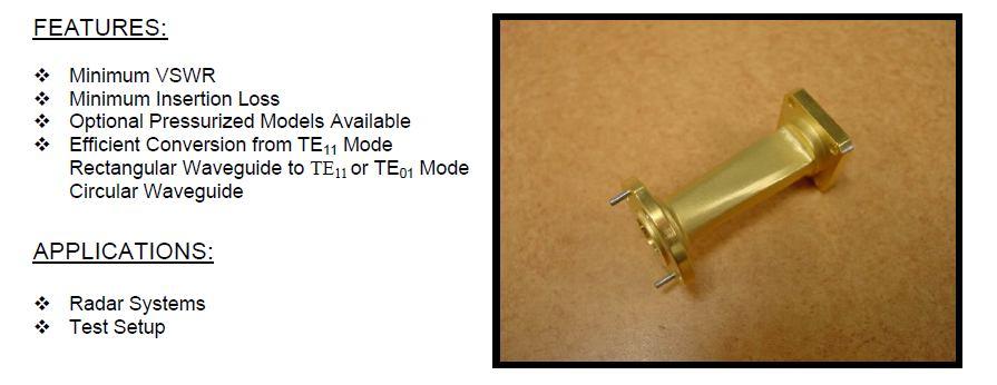
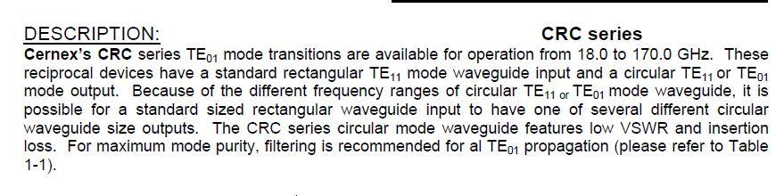
50 Rectangular to circular waveguide transition
51 Waveguides Bends and Twists The size, shape, and dielectric material of a waveguide must be constant throughout its length for energy to move from one end to the other without reflections. Any abrupt change in its size or shape can cause reflections and a loss in overall efficiency. When such a change is necessary, the bends, twists, and joints of the waveguides must meet certain conditions to prevent reflections. Bends Waveguides may be bent in several ways that do not cause reflections. One way is the gradual bend shown in the right part of the following figure. This gradual bend is known as an E bend because it distorts the E fields. The E bend must have a radius greater than two wavelengths to prevent reflections.
52 Waveguides Bends H - bend E - bend Figure 1: Waveguide bends Another common bend is the gradual H bend shown in the leftt part of the figure. It is called an H bend because the H fields are distorted when a waveguide is bent in this manner. Again, the radius of the bend must be greater than two wavelengths to prevent reflections. A sharp bend in either dimension may be used if it meets certain requirements. Notice the two 45-degree bends in figure; the bends are 1/4 λ apart. The reflections that occur at the 45-degree bends cancel each other, leaving the fields as though no reflections have occurred.
.")
53 Waveguide Twists Sometimes the electromagnetic fields must be rotated so that they are in the proper phase to match the phase of the load. This may be accomplished by twisting the waveguide as shown in the figure. The twist must be gradual and greater than two wavelengths (2 λ). Figure 3: Waveguide twist The flexible waveguide allows special bends which some equipment applications might require. It consists of a specially wound ribbon of conductive material, most commonly brass, with the inner surface plated with chromium. Power losses are greater in the flexible waveguide because the inner surfaces are not perfectly smooth. Therefore, it is only used in short sections where no other reasonable solution is available.

54 Phase shifters
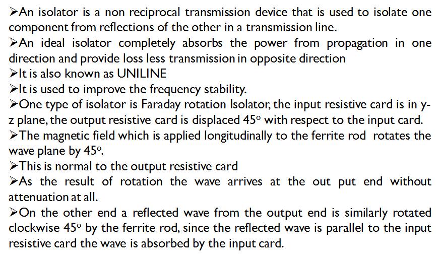
55 Isolator
56 Isolator
57 circulator
58 Circulator
59 Circulator

60 Isolators and circulators

61 Isolators and circulators

62 Isolators and circulators
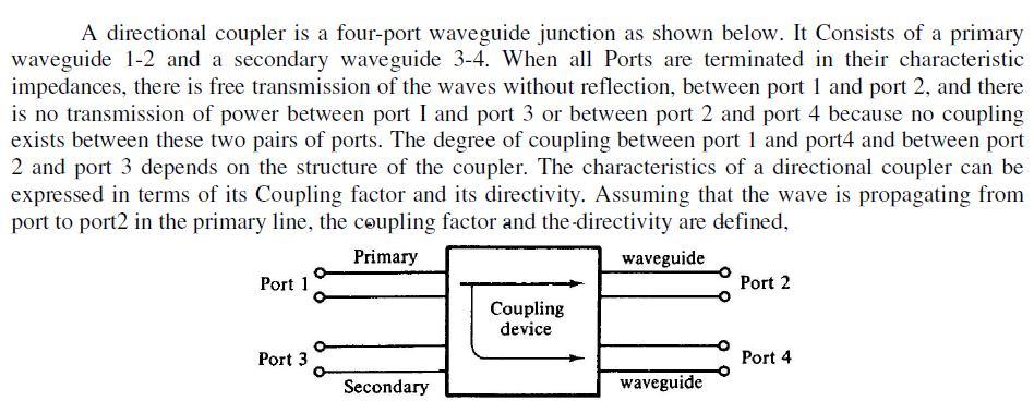
63 Directional Coupler
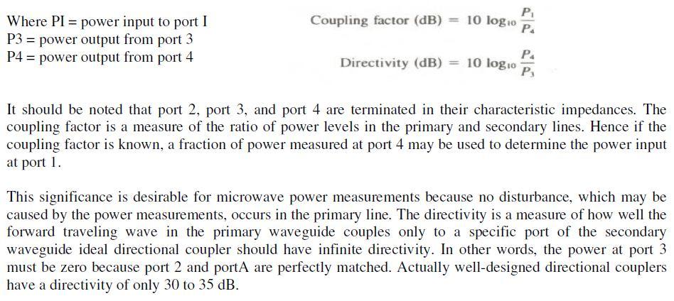
64 Directional Coupler
65 Directional Coupler
66 Directional Coupler
67 Directional Coupler
68 scattering matrix derivation for all components.
69 scattering matrix derivation for all components.
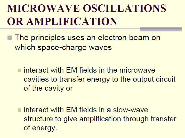
70 UNIT III MICROWAVE VACCUM TUBE DEVICES Introduction Two cavity klystron amplifier Mechanism and mode of operation Power output and efficiency -Applications Reflex klystron oscillator Mechanism and mode of operation-power output Efficiency Mode curve Applications TWT amplifier Principle of operation-gain and applications Magnetron oscillator Hull cut-off voltage mechanism of operation Power output and efficiency Applications Numerical problems.
71
72
73 Types of Microwave Tubes Linear beam tubes (O Type) Crossed Field Tubes (M Type) Eg: Klystron Reflex klystron TWT Eg: Magnetron
74 Linear beam devices Crossed field devices (I) Straight path taken by the electron beam (i) DC magnetic field is in parallel with DC electric field to focus the electron beam A principle feature of such tubes is that electrons travel in a curved path DC magnetic field is perpendicular to DC electric field
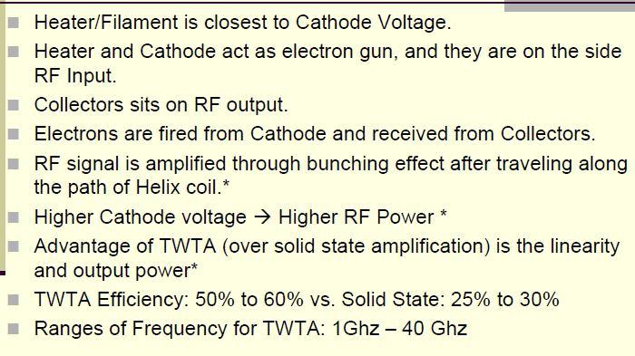
75 Types of Linear Beam Tubes LINEAR BEAM TUBES KLYSTRON TUBES HYBRID TUBES TRAVELING WAVE TUBES TWO CAVITY KLYST MULTI CAVITY KLYST HELIX RING- BAR TWT HELIX BWO REFLEX KLYST LADDE- RTRON TWYSTRON COUPLED CAVITY TWT
76 TWYSTRON KLYSTRON + TWT = TWYSTRON It is hybrid amplifier that uses the combinations of klystron and TWT components
77
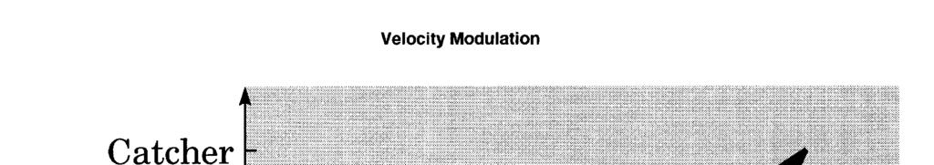
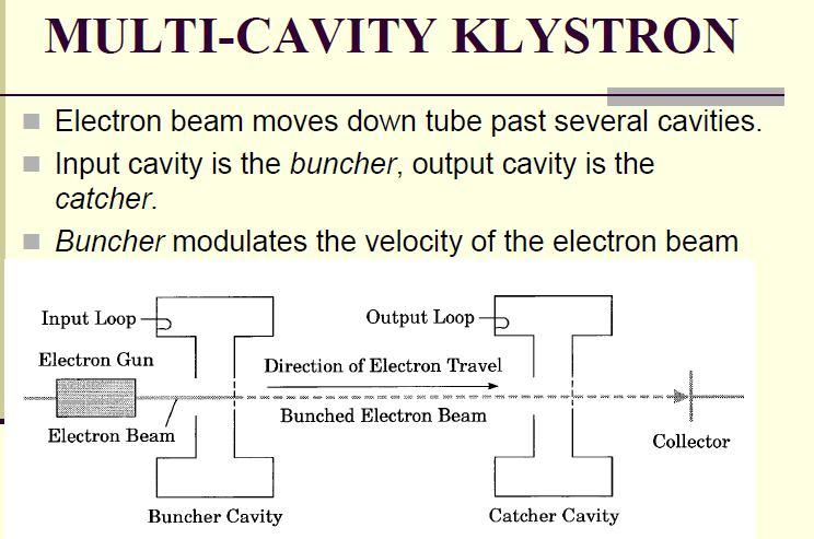
78 Klystron Used in high-power amplifiers Electron beam moves down tube past several cavities. Input cavity is the buncher, output cavity is the catcher. Buncher modulates the velocity of the electron beam
79
80 PRINCIPLE Velocity Modulation Electric field from microwaves at buncher alternately speeds and slows electron beam. This causes electrons to bunch up Electron bunches at catcher induce microwaves with more energy. The cavities form a slow-wave structure

81
82
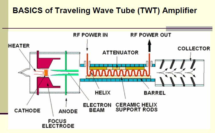
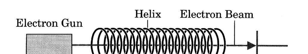
83 Traveling-Wave Tube (TWT) Uses a helix as a slow-wave structure Microwaves input at cathode end of helix, output at anode end Energy is transferred from electron beam to microwaves
84 Traveling-Wave Tube (TWT)
85
86
87
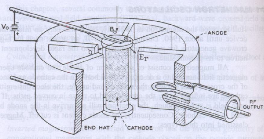
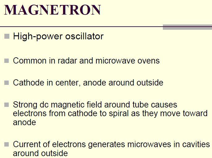
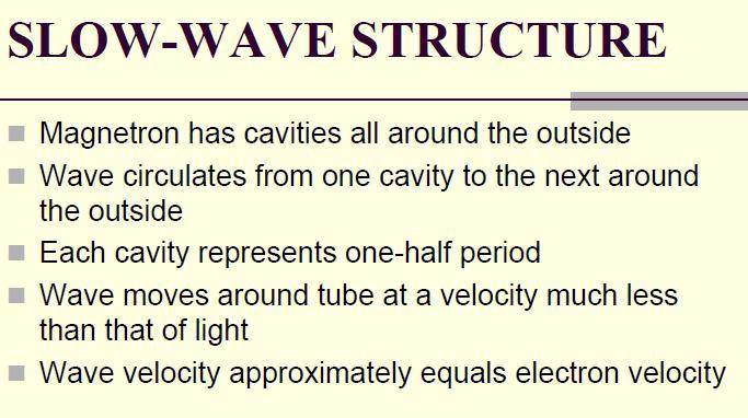
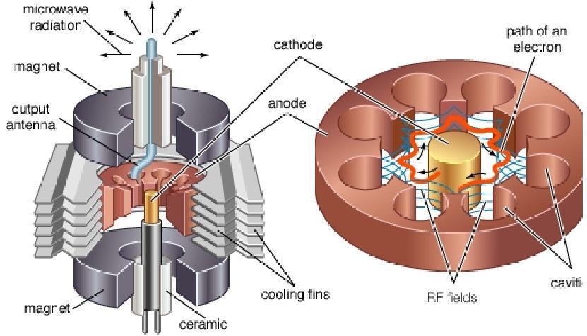
88 Magnetron Oscillator
89
90
91
92
93 UNIT IV MICROWAVE SEMICONDUCTOR DEVICES AND CIRCUITS Principles of tunnel diodes - Varactor and Step recovery diodes Transferred Electron Devices -Gunn diode- Avalanche Transit time devices- IMPATT and TRAPATT Devices- Parametric Amplifiers Introduction to Micro strip Lines, & Monolithic Microwave Integrated circuits-materials, MMIC Fabrication Techniques.
94 Tunnel Diode It is used as high speed switch, of order nano-seconds. Due to tunneling effect it has very fast operation in microwave frequency region. It is a two terminal device in which concentration of dopants is too high. The transient response is being limited by junction capacitance plus stray wiring capacitance. Mostly used in microwave oscillators and amplifiers. It acts as most negative conductance device. Tunnel diodes can be tuned in both mechanically and electrically. The symbol of tunnel diode is as shown below. Tunnel Diode Applications Oscillatory circuits. Microwave circuits. Resistant to nuclear radiation.
95 Varactor Diode These are also known as Varicap diodes. It acts like the variable capacitor. Operations are performed mainly at reverse bias state only. These diodes are very famous due to its capability of changing the capacitance ranges within the circuit in the presence of constant voltage flow. They can able to vary capacitance up to high values. In varactor diode by changing the reverse bias voltage we can decrease or increase the depletion layer. These diodes have many applications as voltage controlled oscillator for cell phones, satellite pre-filters etc. The symbol of varactor diode is given below. Varactor Diode Applications Voltage-controlled capacitors. Voltage-controlled oscillators. Parametric amplifiers. Frequency multipliers. FM transmitters and Phase locked loops in radio, television sets and cellular telephone.

96 Step Recovery Diodes It is also called as snap-off diode or charge-storage diode. These are the special type of diodes which stores the charge from positive pulse and uses in the negative pulse of the sinusoidal signals. The rise time of the current pulse is equal to the snap time. Due to this phenomenon it has speed recovery pulses. The applications of these diodes are in higher order multipliers and in pulse shaper circuits. The cut-off frequency of these diodes is very high which are nearly at Giga hertz order. As multiplier this diode has the cut-off frequency range of 200 to 300 GHz. In the operations which are performing at 10 GHz range these diodes plays a vital role. The efficiency is high for lower order multipliers. The symbol for this diode is as shown below.

97 Transferred Electron Devices

98 Gunn Diode

99 Gunn Diode
100 Avalanche transit time devices The process of having a delay between voltage and current, in avalanche together with transit time, through the material is said to be Negative resistance. The devices that helps to make a diode exhibit this property are called as Avalanche transit time devices. The examples of the devices that come under this category are IMPATT, TRAPATT and BARITT diodes. Let us take a look at each of them, in detail.
101 IMPATT Diode This is a high-power semiconductor diode, used in high frequency microwave applications. The full form IMPATT is IMPact ionization Avalanche Transit Time diode. A voltage gradient when applied to the IMPATT diode, results in a high current. A normal diode will eventually breakdown by this. However, IMPATT diode is developed to withstand all this. A high potential gradient is applied to back bias the diode and hence minority carriers flow across the junction. Application of a RF AC voltage if superimposed on a high DC voltage, the increased velocity of holes and electrons results in additional holes and electrons by thrashing them out of the crystal structure by Impact ionization. If the original DC field applied was at the threshold of developing this situation, then it leads to the avalanche current multiplication and this process continues. This can be understood by the following figure.
102 IMPATT Diode Due to this effect, the current pulse takes a phase shift of 90. However, instead of being there, it moves towards cathode due to the reverse bias applied. The time taken for the pulse to reach cathode depends upon the thickness of n+ layer, which is adjusted to make it 90 phase shift. Now, a dynamic RF negative resistance is proved to exist. Hence, IMPATT diode acts both as an oscillator and an amplifier.
103 IMPATT Diode The efficiency of IMPATT diode is represented as η=[pacpdc]=vavd[iaid]η=[pacpdc]=vavd[iaid] Where, PacPac = AC power Vd&IdVd&Id = DC voltage & current PdcPdc = DC power voltage & current Va&IaVa&Ia = AC
104 IMPATT Diode Disadvantages Following are the disadvantages of IMPATT diode. It is noisy as avalanche is a noisy process Tuning range is not as good as in Gunn diodes Applications Following are the applications of IMPATT diode. Microwave oscillator Microwave generators Modulated output oscillator Receiver local oscillator Negative resistance amplifications Intrusion alarm networks (high Q IMPATT) Police radar (high Q IMPATT) Low power microwave transmitter (high Q IMPATT) FM telecom transmitter (low Q IMPATT) CW Doppler radar transmitter (low Q IMPATT)
105 TRAPATT Diode The full form of TRAPATT diode is TRApped Plasma Avalanche Triggered Transit diode. A microwave generator which operates between hundreds of MHz to GHz. These are high peak power diodes usually n+- p-p+ or p+-nn+ structures with n-type depletion region, width varying from 2.5 to 1.25 µm. The following figure depicts this.
106 TRAPATT Diode The electrons and holes trapped in low field region behind the zone, are made to fill the depletion region in the diode. This is done by a high field avalanche region which propagates through the diode. The following figure shows a graph in which AB shows charging, BC shows plasma formation, DE shows plasma extraction, EF shows residual extraction, and FG shows charging. Let us see what happens at each of the points.
107 TRAPATT Diode A: The voltage at point A is not sufficient for the avalanche breakdown to occur. At A, charge carriers due to thermal generation results in charging of the diode like a linear capacitance. A-B: At this point, the magnitude of the electric field increases. When a sufficient number of carriers are generated, the electric field is depressed throughout the depletion region causing the voltage to decrease from B to C. C: This charge helps the avalanche to continue and a dense plasma of electrons and holes is created. The field is further depressed so as not to let the electrons or holes out of the depletion layer, and traps the remaining plasma. D: The voltage decreases at point D. A long time is required to clear the plasma as the total plasma charge is large compared to the charge per unit time in the external current. E: At point E, the plasma is removed. Residual charges of holes and electrons remain each at one end of the deflection layer.
108 TRAPATT Diode E to F: The voltage increases as the residual charge is removed. F: At point F, all the charge generated internally is removed. F to G: The diode charges like a capacitor. G: At point G, the diode current comes to zero for half a period. The voltage remains constant as shown in the graph above. This state continues until the current comes back on and the cycle repeats. The avalanche zone velocity VsVs is represented as Vs=dxdt=JqNAVs=dxdt=JqNA Where JJ = Current density qq = Electron charge 1.6 x NANA = Doping concentration
109 TRAPATT Diode The avalanche zone will quickly sweep across most of the diode and the transit time of the carriers is represented as τs=lvsτs=lvs Where VsVs = Saturated carrier drift velocity LL = Length of the specimen The transit time calculated here is the time between the injection and the collection. The repeated action increases the output to make it an amplifier, whereas a microwave low pass filter connected in shunt with the circuit can make it work as an oscillator. Applications There are many applications of this diode. Low power Doppler radars Local oscillator for radars Microwave beacon landing system Radio altimeter Phased array radar, etc.
110 Parametric Amplifier
111 Parametric Amplifier
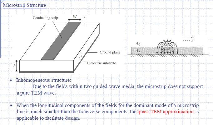
112 Microstrip lines
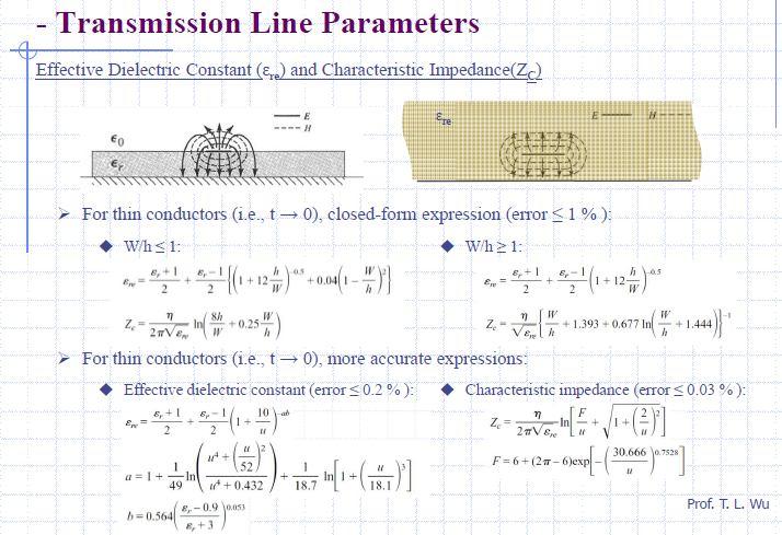
113 Microstrip lines
114 Microstrip lines
115 Microstrip lines
116 Monolithic Microwave Integrated Circuit (MMIC) Microwave ICs are the best alternative to conventional waveguide or coaxial circuits, as they are low in weight, small in size, highly reliable and reproducible. The basic materials used for monolithic microwave integrated circuits are Substrate material Conductor material Dielectric films Resistive films These are so chosen to have ideal characteristics and high efficiency. The substrate on which circuit elements are fabricated is important as the dielectric constant of the material should be high with low dissipation factor, along with other ideal characteristics. The substrate materials used are GaAs, Ferrite/garnet, Aluminum, beryllium, glass and rutile.
117 Monolithic Microwave Integrated Circuit (MMIC) The conductor material is so chosen to have high conductivity, low temperature coefficient of resistance, good adhesion to substrate and etching, etc. Aluminum, copper, gold, and silver are mainly used as conductor materials. The dielectric materials and resistive materials are so chosen to have low loss and good stability. Fabrication Technology In hybrid integrated circuits, the semiconductor devices and passive circuit elements are formed on a dielectric substrate. The passive circuits are either distributed or lumped elements, or a combination of both. Hybrid integrated circuits are of two types. Hybrid IC Miniature Hybrid IC In both the above processes, Hybrid IC uses the distributed circuit elements that are fabricated on IC using a single layer metallization technique, whereas Miniature hybrid IC uses multi-level elements. Most analog circuits use meso-isolation technology to isolate active n-type areas used for FETs and diodes. Planar circuits are fabricated by implanting ions into semi-insulating substrate, and to provide isolation the areas are masked off.
118 UNIT V MICROWAVE MEASUREMENTS Introduction Slotted line carriage Spectrum analyzer Network analyzer Power measurements Schottky barrier diode sensor Bolometer sensor Power sensor High power measurement Insertion loss and attenuation measurement VSWR measurement Low and high VSWR Impedance measurement Frequency measurement Measurement of cavity Q Dielectric measurement of a solid by wave-guide method Antenna measurement Radiation pattern Phase and gain.

119 Slotted Line carriage

120 Spectrum Analyzer
121 Spectrum Analyzer

122 Spectrum Analyzer
123
124
125
126
127
128
129 POWER MEASUREMENT Power is defined as the quantity of energy dissipated or stored per unit time. Methods of measurement of power depend on the frequency of operation, levels of power and whether the power is continuous or pulsed. The range of microwave power is divided into three categories :- i. Low power ( < 0dBm) ii. Medium power ( from 10 mw dbm) iii. High power ( > dbm) The microwave power meter consists of a power sensor, which converts the microwave power to heat energy. The sensors used for power measurements are the Schottky barrier diode, bolometer and the thermocouple.
130 Power Measurement Power may be defined as the rate at which energy is transformed oe made available In almost all cases the power in a d.c. circuit is best measured by separately measuring quantities, V and I and by computing P=VI In case of a.c. circuits the instantaneous power varies continuously as the current and voltage go through a cycle of values The fact that the power factor is involved in the expression for the power means that a wattmeter must be used instead of merely an ammeter and voltmeter.

131 Wattmeter A wattmeter is essentially an inherent combination of an ammeter and a voltmeter and, therefore, consists of two coils known as current coil and pressure coil. Wattmeter connection:

 Supply voltage higher")
132 Measurement of Power in Single Phase A.C. Circuit 3-voltmeter method 2 2 V3 V1 V P 2R 2 2 V cos 2 3 V Disadvantages : (i) Even small errors in measurement of voltages may cause serious errors in the value of power, (ii) Supply voltage higher than normal voltage is required 2 1 2V V 1 V 2 2 2


133 3-Ammeter method The disadvantages of measurement of power by 3 voltmeters are overcome in this method I I I R P cos I I I I I

134 Measurement of power in conjuction with instrument transformers This method is used when the currents and voltages of the circuits to be measured are high Figure below shows a measurement of power with wattmeter in conjunction with instrument transformers in single phase A.C. circuits


135 Measurement of Power in 3-Phase Circuit Measurement of power in 3-phase, 4-wire circuits P=W 1 +W 2 +W 3 Measurement of power in 3-phase, 3-wire circuits P=W 1 +W 2 +W 3
136 SCHOTTKY BARRIER DIODE A zero-biased Schottky Barrier Diode is used as a square-law detector whose output is proportional to the input power. The diode detectors can be used to measure power levels as low as 70dBm.
137 BOLOMETERS A Bolometer is a power sensor whose resistance changes with temperature as it absorbs microwave power. Are power detectors that operate on thermal principles. Since the temperature of the resistance is dependent on the signal power absorbed, the resistance must also be in proportion to the signal power. The two most common types of bolometer are, the barretter and the thermistor. Both are sensitive power detectors and is used to indicate microwatts of power. They are used with bridge circuits to convert resistance to power using a meter or other indicating devices.

138 BOLOMETER
139 Power in DC circuits Power Can be carried out P using I L V a L voltmeter and an ammeter (generally) Two measurement arrangements Wattmeters: Dynamometer Digital wattmeter Thermal wattmeter Hall-power meter
140 DC circuits a) Ammeter measures current which flow into the voltmeter and load b) Voltmeter measures voltage drop across the ammeter in addition to that dropping across the load

141 Dynamometer Power (direct) measurement device for DC and AC systems Accuracy better than 0,25 % Two coils: static and movable Torque is proportional product of current in current coil and current in voltage coil

142 Digital wattmeter (up to 100 khz) Advantages: High-resolution Accuracy Several techniques (multiplication of signals) Electronic multiplier is an analog system which gives as its output a voltage proportional to the power indication required A/D conversion
143 Hall-power meter Coil generates magnetic field which is proportional to load current The sensor excitation current passes through R1 and is proportional to the load voltage Hall voltage is proportional to load power Problems: offset and linearity
144 Power in AC circuits Instantaneous power (time dependence) Mean power (usually the most interesting) Real power (active work), reactive power, apparent power Measures can be done same way as DC circuit (single-phase) p( t) v( t) i( t) P 1 T T 0 p( t) dt
145 AC circuits P V L I L Q V L I L cos sin S P 2 Q 2
146 Low- and Medium-Frequency Power Measurements Three-Voltmeter Method Single-phase arrangements Power in load can be measured using a noninductive resistor and measuring the three voltage Also in DC circuits P L V 2 AC V 2 AB 2R V 2 BC
147 Line-Frequency Power Measurements Polyphase Power Measurements Three-phase systems are most commonly used in industrial applications Energy and power generation and distribution Real power for consumer Reactive power also important (loading) Power can measured several ways Power factor
148 Line-Frequency Power Measurements (2) Four (main) different cases which affects to the measurement arrangements: 1. Symmetrical load with neutral conductor 2. Symmetrical load without neutral conductor 3. Unsymmetrical load with neutral conductor 4. Unsymmetrical load without neutral conductor

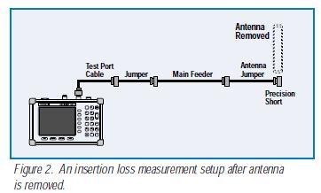
149 Insertion Loss
150 Attenuation Measurement
151
152 VSWR Measurement VSWR is defined as the ratio of the maximum voltage to the minimum voltage in standing wave pattern along the length of a transmission line structure. It varies from 1 to (plus) infinity and is always positive. Unless you have a piece of slotted line-test equipment this is a hard definition to use, especially since the concept of voltage in a microwave structure has many interpretations. Sometimes VSWR is called SWR to avoid using the term voltage and to instead use the concept of power waves. This in turn leads to a mathematical definition of VSWR in terms of a reflection coefficient. A reflection coefficient is defined as the ratio of reflected wave to incident wave at a reference plane. This value varies from -1 (for a shorted load) to +1 (for an open load), and becomes 0 for matched impedance load. It is a complex number. This helps us because we can actually measure power.
153 VSWR Measurement The reflection coefficient, commonly denoted by the Greek letter gamma (Γ), can be calculated from the values of the complex load impedance and the transmission line characteristic impedance which in principle could also be a complex number. Γ = (Z l - Z 0 )/(Z l + Z 0 ) The square of Γ is then the power of the reflected wave, the square hinting at a historical reference to voltage waves. Now we can define VSWR (SWR) as a scalar value: VSWR= (1 + Γ )/(1 - Γ ) or in terms of s-parameters: VSWR= (1 + S 11 )/(1 - S 11 ) This is fine but what has it to do with common usage in ads and specifications. Generally, VSWR is sometimes used as a stand-in for a figure of merit for impedance matching. Sometimes this simplification of a scalar quantity and it s restricted definition can lead to confusion in the matter of a source to load match. Most of the time there is no problem but, technically, VSWR derives from the ratio using the load impedance and the characteristic impedance of the transmission line in which the standing waves reside and not specifically to a source to load match. I prefer to think of VSWR as a figure of merit and to use the reflection coefficient whenever I am trying to solve problems. By the way, if you think you have never experienced a standing wave personally, it's very unlikely. Standing waves in a microwave oven are the reason that food is cooked unevenly (the turntable is a partial solution to that problem). The wavelength of the 2.45 GHz signal is about 12 centimeters, or about five inches. Nulls in the radiation (and heating) will be separated at a distance similar to wavelength.
154 FREQUENCY MEASUREMENT The frequency meter used has a cavity which is coupled to the waveguide by a small coupling hole which is used to absorb only a tiny fraction of energy passing along the waveguide. Adjusting the micrometer of the Frequency Meter will vary the plunger into the cavity. This will alters the cavity size and hence the resonance frequency. The readings on the micrometer scales are calibrated against frequency. As the plunger enters the caviy, its sized is reduced and the frequency increases.
155 The wavemeter is adjusted for maximum or minimum power meter readings depending on whether the cavity is a transmission or absorption type device. With the transmissiontype device, the power meter will be adjusted for a maximum. It only allows frequency close to resonance to be transmitted through them. Other frequencies are reflected down the waveguide. The wavemeter acts as a short circuit for all other frequencies. For the absorption-type wavemeter, the power meter will be adjusted for a minimum. Its absorp power from the line around resonant frequency and act as a short to other frequencies. The absorbing material used is to absorb any unwanted signal that will cause disturbance to the system.
156 VSWR ( VOLTAGE STANDING WAVE RATIO ) MEASUREMENT Used to determine the degree of mismatch between the source and load when the value VSWR 1. Can be measured by using a slotted line. Direct Method Measurement is used for VSWR values upto about 10. Its value can be read directly using a standing wave detector. The measurement consists simply of adjusting attenuator to give an adequate reading, making sure that the frequency is correct and then using the dc voltmeter to measure the detector output at a maximum on the slotted section and then at the nearest minimum.
157 The ratio of the voltage maximum to the minimum gives the VSWR i.e VSWR = V max / V min ISWR = I max / I min = k (V max ) 2 / k (V min ) 2 = ( V max / V min ) 2 = VSWR 2 VSWR = ( I max / I min ) = ISWR
158 Methods used depends on the value of VSWR whether it is high or low. If the load is not exactly matched to the line, standing wave pattern is produced. Reflections can be measured in terms of voltage, current or power. Measurement using voltage is preffered because it is simplicity. When reflection occured, the incident and the reflected waves will reinforce each other in some places, and in others they will tend to cancel each other out.
159 DOUBLE MINIMUM METHOD MEASUREMENT ( VSWR > 10) Double Minimum method is usually employed for VSWR values greater than about 10. E 2 MAX d 2E 2 MIN SWR PATTERN E 2 MIN λ/2 d/2 distance along the line
160 The detector output (proportional to field strength squared) is plotted against position. The probe is moved aling the line to find the minimum value of signal. It is then moved either side to determine 2 positions at which twice as much detector signal is obtained. The distance d between these two positions then gives the VSWR according to the formula : S = 1 + 1/Sin 2 (πd/λ)
161 POWER MEASUREMENT Power is defined as the quantity of energy dissipated or stored per unit time. Methods of measurement of power depend on the frequency of operation, levels of power and whether the power is continuous or pulsed. The range of microwave power is divided into three categories :- i. Low power ( < 0dBm) ii. Medium power ( from 10 mw dbm) iii. High power ( > dbm) The microwave power meter consists of a power sensor, which converts the microwave power to heat energy. The sensors used for power measurements are the Schottky barrier diode, bolometer and the thermocouple.
162 SCHOTTKY BARRIER DIODE A zero-biased Schottky Barrier Diode is used as a square-law detector whose output is proportional to the input power. The diode detectors can be used to measure power levels as low as 70dBm.
163 BOLOMETERS A Bolometer is a power sensor whose resistance changes with temperature as it absorbs microwave power. Are power detectors that operate on thermal principles. Since the temperature of the resistance is dependent on the signal power absorbed, the resistance must also be in proportion to the signal power. The two most common types of bolometer are, the barretter and the thermistor. Both are sensitive power detectors and is used to indicate microwatts of power. They are used with bridge circuits to convert resistance to power using a meter or other indicating devices.

164 BOLOMETER
165 Antenna Measurement
166 Antenna Measurement
167 Gain Measurement

168 Radiation Pattern
DEPARTMENT OF ELECTRONICS AND COMMUNICATION ENGINEERING QUESTION BANK SUBJECT NAME & CODE: EC2403 & RF AND MICROWAVE ENGINEERING UNIT I
 FATIMA MICHAEL COLLEGE OF ENGINEERING & TECHNOLOGY Senkottai Village, Madurai Sivagangai Main Road, Madurai -625 020 An ISO 9001:2008 Certified Institution DEPARTMENT OF ELECTRONICS AND COMMUNICATION ENGINEERING
EC 1402 Microwave Engineering
 SHRI ANGALAMMAN COLLEGE OF ENGINEERING & TECHNOLOGY (An ISO 9001:2008 Certified Institution) SIRUGANOOR,TRICHY-621105. DEPARTMENT OF ELECTRONICS AND COMMUNICATION ENGINEERING EC 1402 Microwave Engineering
. From the above data, determine the network is symmetric or not.
 Velammal College of Engineering and Technology, Madurai Department of Electronics and Communication Engineering Question Bank Subject Name: EC2353 Antennas And Wave Propagation Faculty: Mrs G VShirley
QUESTION BANK SUB. NAME: RF & MICROWAVE ENGINEERING SUB. CODE: EC 2403 BRANCH/YEAR/: ECE/IV UNIT 1 TWO PORT RF NETWORKS- CIRCUIT REPRESENTATION
 QUESTION BANK SUB. NAME: RF & MICROWAVE ENGINEERING SUB. CODE: EC 2403 SEM: VII BRANCH/YEAR/: ECE/IV UNIT 1 TWO PORT RF NETWORKS- CIRCUIT REPRESENTATION 1. What is RF? 2. What is an RF tuner? 3. Define
SHORT QUESTIONS MICROWAVE ENGINEERING UNIT I
 SHORT QUESTIONS MICROWAVE ENGINEERING UNIT I 1. Define Microwave. Microwaves are generally described as electromagnetic waves with frequencies that range from approximately 1GHz to 300 GHz. Therefore,
MICROWAVE MICROWAVE TRAINING BENCH COMPONENT SPECIFICATIONS:
 Microwave section consists of Basic Microwave Training Bench, Advance Microwave Training Bench and Microwave Communication Training System. Microwave Training System is used to study all the concepts of
R.K.YADAV. 2. Explain with suitable sketch the operation of two-cavity Klystron amplifier. explain the concept of velocity and current modulations.
 Question Bank DEPARTMENT OF ELECTRONICS AND COMMUNICATION SUBJECT- MICROWAVE ENGINEERING(EEC-603) Unit-III 1. What are the high frequency limitations of conventional tubes? Explain clearly. 2. Explain
St.MARTIN S ENGINEERING COLLEGE Dhulapally, Secunderabad
 St.MARTIN S ENGINEERING COLLEGE Dhulapally, Secunderabad 500014. Department of Electronics and Communication Engineering SUB: MICROWAVE ENGINEERING SECTION: ECE IV A & B NAME OF THE FACULTY: S RAVI KUMAR,T.SUDHEER
Prepared by: Dr. Rishi Prakash, Dept of Electronics and Communication Engineering Page 1 of 5
 Microwave tunnel diode Some anomalous phenomena were observed in diode which do not follows the classical diode equation. This anomalous phenomena was explained by quantum tunnelling theory. The tunnelling
3. (a) Derive an expression for the Hull cut off condition for cylindrical magnetron oscillator. (b) Write short notes on 8 cavity magnetron [8+8]
![3. (a) Derive an expression for the Hull cut off condition for cylindrical magnetron oscillator. (b) Write short notes on 8 cavity magnetron [8+8]](/thumbs/73/68588725.jpg "3. (a) Derive an expression for the Hull cut off condition for cylindrical magnetron oscillator. (b) Write short notes on 8 cavity magnetron [8+8]") Code No: RR320404 Set No. 1 1. (a) Compare Drift space bunching and Reflector bunching with the help of Applegate diagrams. (b) A reflex Klystron operates at the peak of n=1 or 3 / 4 mode. The dc power
Code No: RR320404 Set No. 1 1. (a) Compare Drift space bunching and Reflector bunching with the help of Applegate diagrams. (b) A reflex Klystron operates at the peak of n=1 or 3 / 4 mode. The dc power
MICROWAVE ENGINEERING-II. Unit- I MICROWAVE MEASUREMENTS
 MICROWAVE ENGINEERING-II Unit- I MICROWAVE MEASUREMENTS 1. Explain microwave power measurement. 2. Why we can not use ordinary diode and transistor in microwave detection and microwave amplification? 3.
MICROWAVE AND RADAR LAB (EE-322-F) LAB MANUAL VI SEMESTER
 LAB MANUAL VI SEMESTER") 1 MICROWAVE AND RADAR LAB (EE-322-F) MICROWAVE AND RADAR LAB (EE-322-F) LAB MANUAL VI SEMESTER RAO PAHALD SINGH GROUP OF INSTITUTIONS BALANA(MOHINDERGARH)123029 Department Of Electronics and Communication
1 MICROWAVE AND RADAR LAB (EE-322-F) MICROWAVE AND RADAR LAB (EE-322-F) LAB MANUAL VI SEMESTER RAO PAHALD SINGH GROUP OF INSTITUTIONS BALANA(MOHINDERGARH)123029 Department Of Electronics and Communication
INSTITUTE OF AERONAUTICAL ENGINEERING (Autonomous) Dundigal, Hyderabad
 Dundigal, Hyderabad") INSTITUTE OF AERONAUTICAL ENGINEERING (Autonomous) Dundigal, Hyderabad - 500 043 ELECTRONICS AND COMMUNICATION ENGINEERING TUTORIAL BANK Name : MICROWAVE ENGINEERING Code : A70442 Class : IV B. Tech I
INSTITUTE OF AERONAUTICAL ENGINEERING (Autonomous) Dundigal, Hyderabad - 500 043 ELECTRONICS AND COMMUNICATION ENGINEERING TUTORIAL BANK Name : MICROWAVE ENGINEERING Code : A70442 Class : IV B. Tech I
MICROWAVE ENGINEERING LAB VIVA QUESTIONS AND ANSWERS
 MICROWAVE ENGINEERING LAB VIVA QUESTIONS AND ANSWERS. Why can t conventional tubes be used at microwave frequencies? Conventional tubes can t be used at microwave frequencies because of transit time effect.
UNIT-4. Microwave Engineering
 UNIT-4 Microwave Engineering Microwave Solid State Devices Two problems with conventional transistors at higher frequencies are: 1. Stray capacitance and inductance. - remedy is interdigital design. 2.Transit
VIVA-VOCE QUESTIONS MICROWAVE LAB
 VIVA-VOCE QUESTIONS MICROWAVE LAB DAWAR PARUL EXPERIMENT NO.-2 1) How are wavelength measured? 2) How do you measure wavelength in a compression wave? 3) What is the units of measure for wavelength? 4)
Dhanalakshmi College of Engineering Department of ECE EC6701 RF and Microwave Engineering Unit 5 Microwave Measurements Part A
 Dhanalakshmi College of Engineering Department of ECE EC6701 RF and Microwave Engineering Unit 5 Microwave Measurements Part A 1. What is the principle by which high power measurements could be done by
Lecture - 19 Microwave Solid State Diode Oscillator and Amplifier
 Basic Building Blocks of Microwave Engineering Prof. Amitabha Bhattacharya Department of Electronics and Communication Engineering Indian Institute of Technology, Kharagpur Lecture - 19 Microwave Solid
Lecture 16 Microwave Detector and Switching Diodes
 Basic Building Blocks of Microwave Engineering Prof. Amitabha Bhattacharya Department of Electronics and Communication Engineering Indian Institute of Technology, Kharagpur Lecture 16 Microwave Detector
Microwave Fundamentals A Survey of Microwave Systems and Devices p. 3 The Relationship of Microwaves to Other Electronic Equipment p.
 Microwave Fundamentals A Survey of Microwave Systems and Devices p. 3 The Relationship of Microwaves to Other Electronic Equipment p. 3 Microwave Systems p. 5 The Microwave Spectrum p. 6 Why Microwave
MAHAVEER INSTITUTE OF SCIENCE & TECHNOLOGY. Microwave and Digital Communications Lab. Department Of Electronics and Communication Engineering
 MAHAVEER INSTITUTE OF SCIENCE & TECHNOLOGY Microwave and Digital Communications Lab Department Of Electronics and Communication Engineering MICROWAVE ENGINEERING LAB List of Experiments: 1.Reflex Klystron
PRINCIPLES OF RADAR. By Members of the Staff of the Radar School Massachusetts Institute of Technology. Third Edition by J.
 PRINCIPLES OF RADAR By Members of the Staff of the Radar School Massachusetts Institute of Technology Third Edition by J. Francis Reintjes ASSISTANT PBOFESSOR OF COMMUNICATIONS MASSACHUSETTS INSTITUTE
Module IV, Lecture 2 DNP experiments and hardware
 Module IV, Lecture 2 DNP experiments and hardware tunnel diodes, Gunn diodes, magnetrons, traveling-wave tubes, klystrons, gyrotrons Dr Ilya Kuprov, University of Southampton, 2013 (for all lecture notes
Microwave Devices and Circuit Design
 Microwave Devices and Circuit Design Ganesh Prasad Srivastava Vijay Laxmi Gupta MICROWAVE DEVICES and CIRCUIT DESIGN GANESH PRASAD SRIVASTAVA Professor (Retired) Department of Electronic Science University
Power and Energy Measurements. MYcsvtu Notes
 Power and Energy Measurements Contest Power measurements DC circuits AC circuits Three-phase systems High-frequency power measurements Energy measurements DC circuits AC circuits Example: Power and energy
Microwave Engineering Third Edition
 Microwave Engineering Third Edition David M. Pozar University of Massachusetts at Amherst WILEY John Wiley & Sons, Inc. ELECTROMAGNETIC THEORY 1 1.1 Introduction to Microwave Engineering 1 Applications
NH-67, TRICHY MAIN ROAD, PULIYUR, C.F , KARUR DT. DEPARTMENT OF ELECTRONICS AND COMMUNICATION ENGINEERING COURSE MATERIAL
 NH-67, TRICHY MAIN ROAD, PULIYUR, C.F. 639 114, KARUR DT. DEPARTMENT OF ELECTRONICS AND COMMUNICATION ENGINEERING COURSE MATERIAL Subject Name: Microwave Engineering Class / Sem: BE (ECE) / VII Subject
MULTIMEDIA UNIVERSITY FACULTY OF ENGINEERING LAB SHEET
 MULTIMEDIA UNIVERSITY FACULTY OF ENGINEERING LAB SHEET ELECTROMAGNETIC THEORY EMF016 MW1 MICROWAVE FREQUENCY AND SWR MEASUREMENTS EM Theory Faculty of Engineering, Multimedia University 1 EXPERIMENT MW1:
PANIMALAR ENGINEERING COLLEGE
 S.NO DEPARTMENT OF ELECTRONICS AND COMMUNICATION ENGINEERING SUBJECT CODE 1 EC6701 2 EC6702 3 EC6703 4 IT6005 5 EC6011 QUESTION BANK SEVENTH SEMESTER (2017-2018) SUBJECT NAME RF & MICROWAVE ENGINEERING
TECHNICAL INFORMATION
 TECHNICAL INFORMATION TECHNOLOGY Y-Junction circulator PORT 1 PORT 2 PORT 3 FIG. 1 The Y-junction circulator uses spinel ferrites or garnet ferrites in the presence of a magnetic bias field, to provide
Chapter 12: Transmission Lines. EET-223: RF Communication Circuits Walter Lara
 Chapter 12: Transmission Lines EET-223: RF Communication Circuits Walter Lara Introduction A transmission line can be defined as the conductive connections between system elements that carry signal power.
To design Phase Shifter. To design bias circuit for the Phase Shifter. Realization and test of both circuits (Doppler Simulator) with
 with") Prof. Dr. Eng. Klaus Solbach Department of High Frequency Techniques University of Duisburg-Essen, Germany Presented by Muhammad Ali Ashraf Muhammad Ali Ashraf 2226956 Outline 1. Motivation 2. Phase Shifters
Prof. Dr. Eng. Klaus Solbach Department of High Frequency Techniques University of Duisburg-Essen, Germany Presented by Muhammad Ali Ashraf Muhammad Ali Ashraf 2226956 Outline 1. Motivation 2. Phase Shifters
Microwave Circuit Design and Measurements Lab. INTRODUCTION TO MICROWAVE MEASUREMENTS: DETECTION OF RF POWER AND STANDING WAVES Lab #2
 EE 458/558 Microwave Circuit Design and Measurements Lab INTRODUCTION TO MICROWAVE MEASUREMENTS: DETECTION OF RF POWER AND STANDING WAVES Lab #2 The purpose of this lab is to gain a basic understanding
Waveguides. Metal Waveguides. Dielectric Waveguides
 Waveguides Waveguides, like transmission lines, are structures used to guide electromagnetic waves from point to point. However, the fundamental characteristics of waveguide and transmission line waves
UNIT VIII-SPECIAL PURPOSE ELECTRONIC DEVICES. 1. Explain tunnel Diode operation with the help of energy band diagrams.
 UNIT III-SPECIAL PURPOSE ELECTRONIC DEICES 1. Explain tunnel Diode operation with the help of energy band diagrams. TUNNEL DIODE: A tunnel diode or Esaki diode is a type of semiconductor diode which is
Fundamentals Of Commercial Doppler Systems
 Fundamentals Of Commercial Doppler Systems Speed, Motion and Distance Measurements I. Introduction MDT manufactures a large variety of microwave oscillators, transceivers, and other components for the
(i) Determine the admittance parameters of the network of Fig 1 (f) and draw its - equivalent circuit.
 Determine the admittance parameters of the network of Fig 1 (f) and draw its - equivalent circuit.") I.E.S-(Conv.)-1995 ELECTRONICS AND TELECOMMUNICATION ENGINEERING PAPER - I Some useful data: Electron charge: 1.6 10 19 Coulomb Free space permeability: 4 10 7 H/m Free space permittivity: 8.85 pf/m Velocity
I.E.S-(Conv.)-1995 ELECTRONICS AND TELECOMMUNICATION ENGINEERING PAPER - I Some useful data: Electron charge: 1.6 10 19 Coulomb Free space permeability: 4 10 7 H/m Free space permittivity: 8.85 pf/m Velocity
COOPERATIVE PATENT CLASSIFICATION
 CPC H H03 COOPERATIVE PATENT CLASSIFICATION ELECTRICITY (NOTE omitted) BASIC ELECTRONIC CIRCUITRY H03B GENERATION OF OSCILLATIONS, DIRECTLY OR BY FREQUENCY-CHANGING, BY CIRCUITS EMPLOYING ACTIVE ELEMENTS
LESSON PLAN. LESSON PLAN DURATION : - 15 weeks (from JULY 2018 to NOVEMBER 2018)
") LESSON PLAN NAME OF THE FACULTY DISCIPLINE SEMESTER SUBJECT : - HIMANSHU YADAV : - ECE : - FIFTH : - MICROWAVE ENGG LESSON PLAN DURATION : - 15 weeks (from JULY 2018 to NOVEMBER 2018) WORK LOAD (LECTURE/PRACTICAL)
LESSON PLAN NAME OF THE FACULTY DISCIPLINE SEMESTER SUBJECT : - HIMANSHU YADAV : - ECE : - FIFTH : - MICROWAVE ENGG LESSON PLAN DURATION : - 15 weeks (from JULY 2018 to NOVEMBER 2018) WORK LOAD (LECTURE/PRACTICAL)
Magnetron. Physical construction of a magnetron
 anode block interaction space cathode filament leads Magnetron The magnetron is a high-powered vacuum tube that works as self-excited microwave oscillator. Crossed electron and magnetic fields are used
Chapter 21. Alternating Current Circuits and Electromagnetic Waves
 Chapter 21 Alternating Current Circuits and Electromagnetic Waves AC Circuit An AC circuit consists of a combination of circuit elements and an AC generator or source The output of an AC generator is sinusoidal
ECRH on the Levitated Dipole Experiment
 ECRH on the Levitated Dipole Experiment S. Mahar, J. Kesner, A.C. Boxer, J.E. Ellsworth, I. Karim, A. Roach MIT PSFC A.K. Hansen, D.T. Garnier, M.E. Mauel, E.E.Ortiz Columbia University Presented at the
For the mechanical system of figure shown above:
 I.E.S-(Conv.)-00 ELECTRONICS AND TELECOMMUNICATION ENGINEERING PAPER - I Time Allowed: Three Hours Maximum Marks : 0 Candidates should attempt any FIVE questions. Some useful data: Electron charge : 1.6
CHAPTER 4. Practical Design
 CHAPTER 4 Practical Design The results in Chapter 3 indicate that the 2-D CCS TL can be used to synthesize a wider range of characteristic impedance, flatten propagation characteristics, and place passive
The Basics of Patch Antennas, Updated
 The Basics of Patch Antennas, Updated By D. Orban and G.J.K. Moernaut, Orban Microwave Products www.orbanmicrowave.com Introduction This article introduces the basic concepts of patch antennas. We use
EE 3324 Electromagnetics Laboratory
 EE 3324 Electromagnetics Laboratory Experiment #10 Microstrip Circuits and Measurements 1. Objective The objective of Experiment #8 is to investigate the application of microstrip technology. A precision
SRM UNIVERSITY FACULTY OF ENGINEERING AND TECHNOLOGY SCHOOL OF ELECTRONICS AND ELECTRICAL ENGINEERING DEPARTMENT OF TCE COURSE PLAN
 SRM UNIVERSITY FACULTY OF ENGINEERING AND TECHNOLOGY SCHOOL OF ELECTRONICS AND ELECTRICAL ENGINEERING DEPARTMENT OF TCE COURSE PLAN Course Code : TE1018 Course Title : Microwave Radio And Optical Fiber
Lab 12 Microwave Optics.
 b Lab 12 Microwave Optics. CAUTION: The output power of the microwave transmitter is well below standard safety levels. Nevertheless, do not look directly into the microwave horn at close range when the
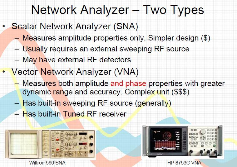
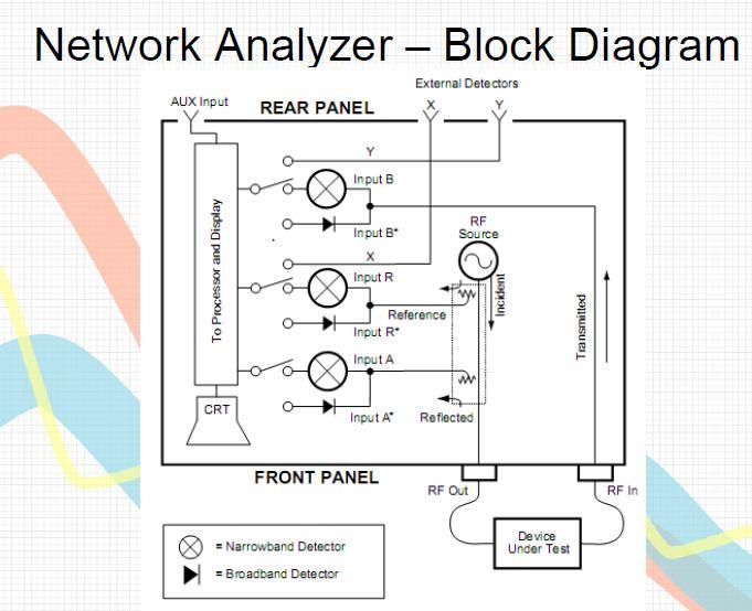
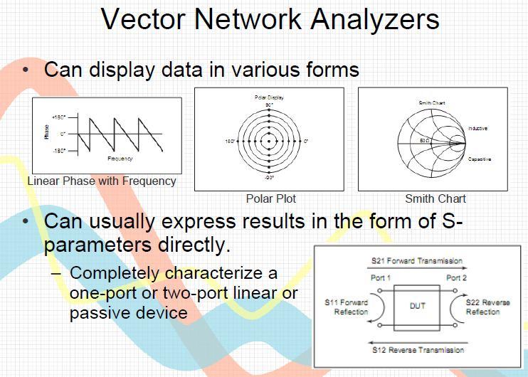
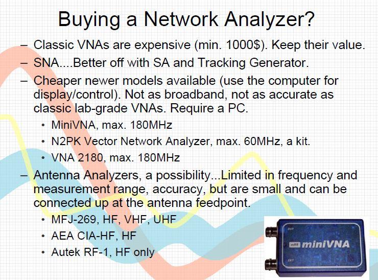
Measurements 2: Network Analysis
 Measurements 2: Network Analysis Fritz Caspers CAS, Aarhus, June 2010 Contents Scalar network analysis Vector network analysis Early concepts Modern instrumentation Calibration methods Time domain (synthetic
KOM2751 Analog Electronics :: Dr. Muharrem Mercimek :: YTU - Control and Automation Dept. 1 1 (CONT D) DIODES
 DIODES") KOM2751 Analog Electronics :: Dr. Muharrem Mercimek :: YTU - Control and Automation Dept. 1 1 (CONT D) DIODES Most of the content is from the textbook: Electronic devices and circuit theory, Robert L.
KOM2751 Analog Electronics :: Dr. Muharrem Mercimek :: YTU - Control and Automation Dept. 1 1 (CONT D) DIODES Most of the content is from the textbook: Electronic devices and circuit theory, Robert L.
The Principle V(SWR) The Result. Mirror, Mirror, Darkly, Darkly
 The Result. Mirror, Mirror, Darkly, Darkly") The Principle V(SWR) The Result Mirror, Mirror, Darkly, Darkly 1 Question time!! What do you think VSWR (SWR) mean to you? What does one mean by a transmission line? Coaxial line Waveguide Water pipe Tunnel
The Principle V(SWR) The Result Mirror, Mirror, Darkly, Darkly 1 Question time!! What do you think VSWR (SWR) mean to you? What does one mean by a transmission line? Coaxial line Waveguide Water pipe Tunnel
Introduction: Planar Transmission Lines
 Chapter-1 Introduction: Planar Transmission Lines 1.1 Overview Microwave integrated circuit (MIC) techniques represent an extension of integrated circuit technology to microwave frequencies. Since four
7. Experiment K: Wave Propagation
 7. Experiment K: Wave Propagation This laboratory will be based upon observing standing waves in three different ways, through coaxial cables, in free space and in a waveguide. You will also observe some
Navy Electricity and Electronics Training Series
 NONRESIDENT TRAINING COURSE Navy Electricity and Electronics Training Series Module 11 Microwave Principles NAVEDTRA 14183 DISTRIBUTION STATEMENT A: Approved for public release; distribution is unlimited.
9/28/2010. Chapter , The McGraw-Hill Companies, Inc.
 Chapter 4 Sensors are are used to detect, and often to measure, the magnitude of something. They basically operate by converting mechanical, magnetic, thermal, optical, and chemical variations into electric
Amateur Extra Manual Chapter 9.4 Transmission Lines
 9.4 TRANSMISSION LINES (page 9-31) WAVELENGTH IN A FEED LINE (page 9-31) VELOCITY OF PROPAGATION (page 9-32) Speed of Wave in a Transmission Line VF = Velocity Factor = Speed of Light in a Vacuum Question
EDC Lecture Notes UNIT-1
 P-N Junction Diode EDC Lecture Notes Diode: A pure silicon crystal or germanium crystal is known as an intrinsic semiconductor. There are not enough free electrons and holes in an intrinsic semi-conductor
EC Transmission Lines And Waveguides
 EC6503 - Transmission Lines And Waveguides UNIT I - TRANSMISSION LINE THEORY A line of cascaded T sections & Transmission lines - General Solution, Physical Significance of the Equations 1. Define Characteristic
Review Energy Bands Carrier Density & Mobility Carrier Transport Generation and Recombination
 Review Energy Bands Carrier Density & Mobility Carrier Transport Generation and Recombination Current Transport: Diffusion, Thermionic Emission & Tunneling For Diffusion current, the depletion layer is
Microwave Circuits 1.1 INTRODUCTION
 Microwave Circuits 1.1 INTRODUCTION The term microwave circuits means different things to different people. The prefix micro comes from the Greek fiikpog (micros) and among its various meanings has the
Microwave Circuit Analysis and Amplifier Design
 Microwave Circuit Analysis and Amplifier Design SAMUEL Y. LIAO Professor of Electrical Engineering California State University, Fresno PRENTICE-HALL, INC., Englewood Cliffs, New Jersey 07632 Contents PREFACE
Dinesh Micro Waves & Electronics
 Wave Guide Components RECTANGULAR WAVE GUDES Dinesh Microwaves and Electronics manufacturers of high power waveguide in the microwaves industry, this experience had resulted in designing, manufacturing
DEVELOPMENT AND PRODUCTION OF HYBRID CIRCUITS FOR MICROWAVE RADIO LINKS
 Electrocomponent Science and Technology 1977, Vol. 4, pp. 79-83 (C)Gordon and Breach Science Publishers Ltd., 1977 Printed in Great Britain DEVELOPMENT AND PRODUCTION OF HYBRID CIRCUITS FOR MICROWAVE RADIO
APPLIED ELECTROMAGNETICS: EARLY TRANSMISSION LINES APPROACH
 APPLIED ELECTROMAGNETICS: EARLY TRANSMISSION LINES APPROACH STUART M. WENTWORTH Auburn University IICENTBN Nlfll 1807; WILEY 2 OO 7 ; Ttt^TlLtftiTTu CONTENTS CHAPTER1 Introduction 1 1.1 1.2 1.3 1.4 1.5
EC6011-ELECTROMAGNETICINTERFERENCEANDCOMPATIBILITY
 EC6011-ELECTROMAGNETICINTERFERENCEANDCOMPATIBILITY UNIT-3 Part A 1. What is an opto-isolator? [N/D-16] An optoisolator (also known as optical coupler,optocoupler and opto-isolator) is a semiconductor device
GUJARAT TECHNOLOGICAL UNIVERSITY, AHMEDABAD, GUJARAT COURSE CURRICULUM COURSE TITLE: MICROWAVE & RADAR ENGINEERING (COURSE CODE: )
") GUJARAT TECHNOLOGICAL UNIVERSITY, AHMEDABAD, GUJARAT COURSE CURRICULUM COURSE TITLE: MICROWAVE & RADAR ENGINEERING (COURSE CODE: 3351103) Diploma Programme in which this course is offered Electronics and
GUJARAT TECHNOLOGICAL UNIVERSITY, AHMEDABAD, GUJARAT COURSE CURRICULUM COURSE TITLE: MICROWAVE & RADAR ENGINEERING (COURSE CODE: 3351103) Diploma Programme in which this course is offered Electronics and
CHAPTER 6 CARBON NANOTUBE AND ITS RF APPLICATION
 CHAPTER 6 CARBON NANOTUBE AND ITS RF APPLICATION 6.1 Introduction In this chapter we have made a theoretical study about carbon nanotubes electrical properties and their utility in antenna applications.
Chapter 6. FM Circuits
 Chapter 6 FM Circuits Topics Covered 6-1: Frequency Modulators 6-2: Frequency Demodulators Objectives You should be able to: Explain the operation of an FM modulators and demodulators. Compare and contrast;
MICROWAVE AND RADAR ENGINEERING (EE 322 F) LIST OF EXPERIMENTS. S.NO. NAME OF THE EXPERIMENT Page No.
 LIST OF EXPERIMENTS. S.NO. NAME OF THE EXPERIMENT Page No.") LIST OF EXPERIMENTS S.NO. NAME OF THE EXPERIMENT Page No. 1 To study wave guide components. 1-3 2 To study the characteristics of Gunn oscillator &Gun diode as 4-6 modulated source. 3 Study of wave guide
LIST OF EXPERIMENTS S.NO. NAME OF THE EXPERIMENT Page No. 1 To study wave guide components. 1-3 2 To study the characteristics of Gunn oscillator &Gun diode as 4-6 modulated source. 3 Study of wave guide
Detection Beyond 100µm Photon detectors no longer work ("shallow", i.e. low excitation energy, impurities only go out to equivalent of
 Detection Beyond 100µm Photon detectors no longer work ("shallow", i.e. low excitation energy, impurities only go out to equivalent of 100µm) A few tricks let them stretch a little further (like stressing)
Objectives of transmission lines
 Introduction to Transmission Lines Applications Telephone Cable TV (CATV, or Community Antenna Television) Broadband network High frequency (RF) circuits, e.g., circuit board, RF circuits, etc. Microwave
LRL Model 550B-SS Microwave Training Kit
 MICROWAVES FOR EVERYONE LRL Model 550B-SS Microwave Training Kit Microwave Training Kit 5 Experiments I-95 Industrial Park 651 Winks Lane Bensalem, PA 1900 800.53.399 15.638.1100 3rd edition INITIAL SET-UP
TERM PAPER OF ELECTROMAGNETIC
 TERM PAPER OF ELECTROMAGNETIC COMMUNICATION SYSTEMS TOPIC: LOSSES IN TRANSMISSION LINES ABSTRACT: - The transmission lines are considered to be impedance matching circuits designed to deliver rf power
Micro-sensors - what happens when you make "classical" devices "small": MEMS devices and integrated bolometric IR detectors
 Micro-sensors - what happens when you make "classical" devices "small": MEMS devices and integrated bolometric IR detectors Dean P. Neikirk 1 MURI bio-ir sensors kick-off 6/16/98 Where are the targets
ELEC4604. RF Electronics. Experiment 2
 ELEC4604 RF Electronics Experiment MICROWAVE MEASUREMENT TECHNIQUES 1. Introduction and Objectives In designing the RF front end of a microwave communication system it is important to appreciate that the
Equivalent Circuit Model Overview of Chip Spiral Inductors
 Equivalent Circuit Model Overview of Chip Spiral Inductors The applications of the chip Spiral Inductors have been widely used in telecommunication products as wireless LAN cards, Mobile Phone and so on.
PA FAN PLATE ASSEMBLY 188D6127G1 SYMBOL PART NO. DESCRIPTION. 4 SBS /10 Spring nut. 5 19A702339P510 Screw, thread forming, flat head.
 MAINTENANCE MANUAL 851-870 MHz, 110 WATT POWER AMPLIFIER 19D902797G5 TABLE OF CONTENTS Page DESCRIPTION.............................................. Front Page SPECIFICATIONS.................................................
A HIGH-POWER LOW-LOSS MULTIPORT RADIAL WAVEGUIDE POWER DIVIDER
 Progress In Electromagnetics Research Letters, Vol. 31, 189 198, 2012 A HIGH-POWER LOW-LOSS MULTIPORT RADIAL WAVEGUIDE POWER DIVIDER X.-Q. Li *, Q.-X. Liu, and J.-Q. Zhang School of Physical Science and
I.E.S-(Conv.)-1992 Time Allowed : Three Hours
-1992 Time Allowed : Three Hours") I.E.S-(Conv.)-1992 ELECTRONICS AND TELECOMMUNICATION ENGINEERING PAPER - I Time Allowed : Three Hours Maximum Marks: 0 Candidates should attempt question No. 1 which is compulsory and any FOUR of the remaining
I.E.S-(Conv.)-1992 ELECTRONICS AND TELECOMMUNICATION ENGINEERING PAPER - I Time Allowed : Three Hours Maximum Marks: 0 Candidates should attempt question No. 1 which is compulsory and any FOUR of the remaining
Dhanalakshmi College of Engineering Department of ECE EC6701 RF and Microwave Engineering Unit 4 Part A
 Dhanalakshmi College of Engineering Department of ECE EC6701 RF and Microwave Engineering Unit 4 Part A 1. What is magnetron? [N/D-16] an electron tube for amplifying or generating microwaves, with the
Analog Electronic Circuits
 Analog Electronic Circuits Chapter 1: Semiconductor Diodes Objectives: To become familiar with the working principles of semiconductor diode To become familiar with the design and analysis of diode circuits
1. Explain how Doppler direction is identified with FMCW radar. Fig Block diagram of FM-CW radar. f b (up) = f r - f d. f b (down) = f r + f d
 = f r - f d. f b (down) = f r + f d") 1. Explain how Doppler direction is identified with FMCW radar. A block diagram illustrating the principle of the FM-CW radar is shown in Fig. 4.1.1 A portion of the transmitter signal acts as the reference
1. Explain how Doppler direction is identified with FMCW radar. A block diagram illustrating the principle of the FM-CW radar is shown in Fig. 4.1.1 A portion of the transmitter signal acts as the reference
Limiter Diodes Features Description Chip Dimensions Model DOT Diameter (Typ.) Chip Number St l Style Inches 4 11
 Chip Number St l Style Inches 4 11") Features Low Loss kw Coarse Limiters 200 Watt Midrange Limiters 10 mw Clean Up Limiters 210 20 Description Alpha has pioneered the microwave limiter diode. Because all phases of manufacturing, from design
Features Low Loss kw Coarse Limiters 200 Watt Midrange Limiters 10 mw Clean Up Limiters 210 20 Description Alpha has pioneered the microwave limiter diode. Because all phases of manufacturing, from design
ELECTRONIC DEVICES AND CIRCUITS
 ELECTRONIC DEVICES AND CIRCUITS 1. At room temperature the current in an intrinsic semiconductor is due to A. holes B. electrons C. ions D. holes and electrons 2. Work function is the maximum energy required
ECEN 4634/5634, MICROWAVE AND RF LABORATORY
 ECEN 4634/5634, MICROWAVE AND RF LABORATORY Final Exam December 18, 2017 7:30-10:00pm 150 minutes, closed book, 1 sheet allowed, no calculators (estimates need to be within 3dB) Part 1 (60%). Briefly answer
Γ L = Γ S =
 TOPIC: Microwave Circuits Q.1 Determine the S parameters of two port network consisting of a series resistance R terminated at its input and output ports by the characteristic impedance Zo. Q.2 Input matching
LECTURE 6 BROAD-BAND AMPLIFIERS
 ECEN 54, Spring 18 Active Microwave Circuits Zoya Popovic, University of Colorado, Boulder LECTURE 6 BROAD-BAND AMPLIFIERS The challenge in designing a broadband microwave amplifier is the fact that the
UNIT 2. Q.1) Describe the functioning of standard signal generator. Ans. Electronic Measurements & Instrumentation
 Describe the functioning of standard signal generator. Ans. Electronic Measurements & Instrumentation") UNIT 2 Q.1) Describe the functioning of standard signal generator Ans. STANDARD SIGNAL GENERATOR A standard signal generator produces known and controllable voltages. It is used as power source for the
UNIT 2 Q.1) Describe the functioning of standard signal generator Ans. STANDARD SIGNAL GENERATOR A standard signal generator produces known and controllable voltages. It is used as power source for the
ECEN 5014, Spring 2009 Special Topics: Active Microwave Circuits Zoya Popovic, University of Colorado, Boulder
 ECEN 5014, Spring 2009 Special Topics: Active Microwave Circuits Zoya opovic, University of Colorado, Boulder LECTURE 3 MICROWAVE AMLIFIERS: INTRODUCTION L3.1. TRANSISTORS AS BILATERAL MULTIORTS Transistor
UNIVERSITI MALAYSIA PERLIS
 UNIVERSITI MALAYSIA PERLIS SCHOOL OF COMPUTER & COMMUNICATIONS ENGINEERING EKT 341 LABORATORY MODULE LAB 2 Antenna Characteristic 1 Measurement of Radiation Pattern, Gain, VSWR, input impedance and reflection
Frequently Asked Questions GE6252 BEEE UNIT I ELECTRICAL CIRCUITS AND MEASUREMENTS
 Frequently Asked Questions GE6252 BEEE UNIT I ELECTRICAL CIRCUITS AND MEASUREMENTS 1. What is charge? 2. Define current. 3. Under what condition AC circuit said to be resonant? 4. What do you meant by
Chapter 13: Microwave Communication Systems
 Chapter 13: Microwave Communication Systems Chapter 13 Objectives At the conclusion of this chapter, the reader will be able to: Describe the differences between microwave and lower-frequency communications
Manual For Experiment
 AT-RF3030 RF EDUCATION EXPERIMENT SYSTEM Manual For Experiment SHENZHEN ATTEN ELECTRONICS CO.,LTD. 1 Quality assurance SHENZHEN ATTEN ELECTRONICS Co., Ltd. offers the quality assurance for this product.
UNIT 3: FIELD EFFECT TRANSISTORS
 FIELD EFFECT TRANSISTOR: UNIT 3: FIELD EFFECT TRANSISTORS The field effect transistor is a semiconductor device, which depends for its operation on the control of current by an electric field. There are
Low Cost Mixer for the 10.7 to 12.8 GHz Direct Broadcast Satellite Market
 Low Cost Mixer for the.7 to 12.8 GHz Direct Broadcast Satellite Market Application Note 1136 Introduction The wide bandwidth requirement in DBS satellite applications places a big performance demand on
 I.E.S-(Conv.)-2007 ELECTRONICS AND TELECOMMUNICATION ENGINEERING PAPER - II Time Allowed: 3 hours Maximum Marks : 200 Candidates should attempt Question No. 1 which is compulsory and FOUR more questions
9. Microwaves. 9.1 Introduction. Safety consideration
 MW 9. Microwaves 9.1 Introduction Electromagnetic waves with wavelengths of the order of 1 mm to 1 m, or equivalently, with frequencies from 0.3 GHz to 0.3 THz, are commonly known as microwaves, sometimes
"Natural" Antennas. Mr. Robert Marcus, PE, NCE Dr. Bruce C. Gabrielson, NCE. Security Engineering Services, Inc. PO Box 550 Chesapeake Beach, MD 20732
 Published and presented: AFCEA TEMPEST Training Course, Burke, VA, 1992 Introduction "Natural" Antennas Mr. Robert Marcus, PE, NCE Dr. Bruce C. Gabrielson, NCE Security Engineering Services, Inc. PO Box
2. The Basic principle of optical fibre (Or) Working principle of optical fibre (or) Total internal reflection
 Working principle of optical fibre (or) Total internal reflection") Introduction Fibre optics deals with the light propagation through thin glass fibres. Fibre optics plays an important role in the field of communication to transmit voice, television and digital data signals
Introduction Fibre optics deals with the light propagation through thin glass fibres. Fibre optics plays an important role in the field of communication to transmit voice, television and digital data signals
1. What is the unit of electromotive force? (a) volt (b) ampere (c) watt (d) ohm. 2. The resonant frequency of a tuned (LRC) circuit is given by
 volt (b) ampere (c) watt (d) ohm. 2. The resonant frequency of a tuned (LRC) circuit is given by") Department of Examinations, Sri Lanka EXAMINATION FOR THE AMATEUR RADIO OPERATORS CERTIFICATE OF PROFICIENCY ISSUED BY THE DIRECTOR GENERAL OF TELECOMMUNICATIONS, SRI LANKA 2004 (NOVICE CLASS) Basic Electricity,
Department of Examinations, Sri Lanka EXAMINATION FOR THE AMATEUR RADIO OPERATORS CERTIFICATE OF PROFICIENCY ISSUED BY THE DIRECTOR GENERAL OF TELECOMMUNICATIONS, SRI LANKA 2004 (NOVICE CLASS) Basic Electricity,