Hybrid Silicon Integration. R. Jones et al.
|
|
|
- Rosamond Kelly
- 5 years ago
- Views:
Transcription
1 Hybrid Silicon Integration R. Jones 1, H. D. Park 3, A. W. Fang 3, J. E. Bowers 3, O. Cohen 2, O. Raday 2, and M. J. Paniccia 1 1 Intel Corporation, 2200 Mission College Blvd, SC12-326, Santa Clara, California 95054, USA 2 Intel Corporation, S.B.I. Park Har Hotzvim, Jerusalem, 91031, Israel 3 University of California, Santa Barbara, Department of Electrical and Computer Engineering, Santa Barbara, CA 93106, USA Corresponding author Richard.jones@intel.com 1 / 23
2 Hybrid Silicon Integration R. Jones 1, H. D. Park 3, A. W. Fang 3, J. E. Bowers 3, O. Cohen 2, O. Raday 2, and M. J. Paniccia 1 1 Intel Corporation, 2200 Mission College Blvd, SC12-326, Santa Clara, California 95054, USA 2 Intel Corporation, S.B.I. Park Har Hotzvim, Jerusalem, 91031, Israel 3 University of California, Santa Barbara, Department of Electrical and Computer Engineering, Santa Barbara, CA 93106, USA Corresponding author Richard.jones@intel.com Abstract: An overview is presented of the hybrid AlGaInAs-silicon platform that enables wafer level integration of III-V optoelectronic devices with silicon photonic devices based on silicon-on-insulator (SOI). Wafer bonding AlGaInAs quantum wells to an SOI wafer allows large scale hybrid integration without any critical alignment steps. Discrete hybrid silicon optical amplifiers, lasers and photodetectors are described, and the integration of a ring laser with on-chip and photo-detector and amplified spontaneous emission (ASE) seed to enable unidirectional lasing. 2 / 23
3 1. Introduction Silicon photonics has the potential to provide highly integrated, low-cost, optical components using the same CMOS-based manufacturing techniques that revolutionized the micro-electronics industry. This is important as lowering the cost of optical interconnects would enable high-bandwidth optical communication links in and around personal computers and servers where their cost today is prohibitively expensive. Silicon has many properties that make it ideal as a material for integrated optics. Silicon s band edge at 1.1 um makes it compatible with long wavelength infra-red communication links, its high refractive index contrast with its native oxide ( n~2) enables small-footprint integrated optical devices, and of course high volume manufacturing techniques can be used to fabricate silicon photonic chips at low cost [ 1, 2 ]. Both passive and active photonic devices have been demonstrated built on silicon-oninsulator (SOI) substrates such as WDM splitters for fiber to the home applications [ 3 ] and high speed optical modulators [ 4 ]. As silicon is transparent above 1.1um it cannot be used as a photo-detector in the 1.31um and 1.55um communication windows but other CMOS compatible group IV materials have been suggested for this role, e.g. germanium [ 5 ]. The key issue for material compatibility is the ability to process devices on the same SOI wafer as other silicon components simultaneously across the wafer. In fact all the devices needed for an optical link can be fabricated from silicon or compatible materials apart from the laser. Due to silicon s indirect band gap light emission is very inefficient [ 2 ] and currently the preferred method of integrating lasers with silicon chips is to align and then attach individual prefabricated lasers to silicon waveguides one at a time. This has the key drawback that the assembly time increases as the required number of lasers increases. Consider, for example, a typical 6-inch SOI wafer containing 44 silicon die each requiring 8 lasers, individually attaching 352 lasers to each wafer is clearly not a time- or cost-efficient solution. A better approach would be to use the same wafer-scale fabrication techniques to manufacture both the silicon photonic components and the laser. That is the aim of the hybrid laser work discussed here. 2. Hybrid silicon device architecture The hybrid-silicon platform allows silicon photonic devices to be integrated with active optoelectronic devices more commonly associated with III-V materials such as: electrically pumped lasers; amplifiers; wavelength converters; and photo-detectors. A typical device cross-section is shown in Fig. 1, with the SOI and III-V regions labeled on the left-hand side of the schematic. An unprocessed III-V wafer is first bonded to a silicon wafer patterned with optical waveguides, followed by the III-V processing using standard planar-fabrication techniques. Because bonding is done before laser fabrication, there is no alignment needed between the un-patterned III-V wafer and the patterned silicon wafer. Wafer bonding the two material systems addresses the difficulties of lattice mismatch that occur when trying to grow III-V materials directly onto silicon. The low-temperature bonding allows for the different thermal expansion coefficients of the two materials, and eliminates any pronounced stress in the final bonded system. Bonding may be done at the wafer, partial-wafer or die-level, depending on the exact application and economics of the device being fabricated. FIGURE 1 3 / 23
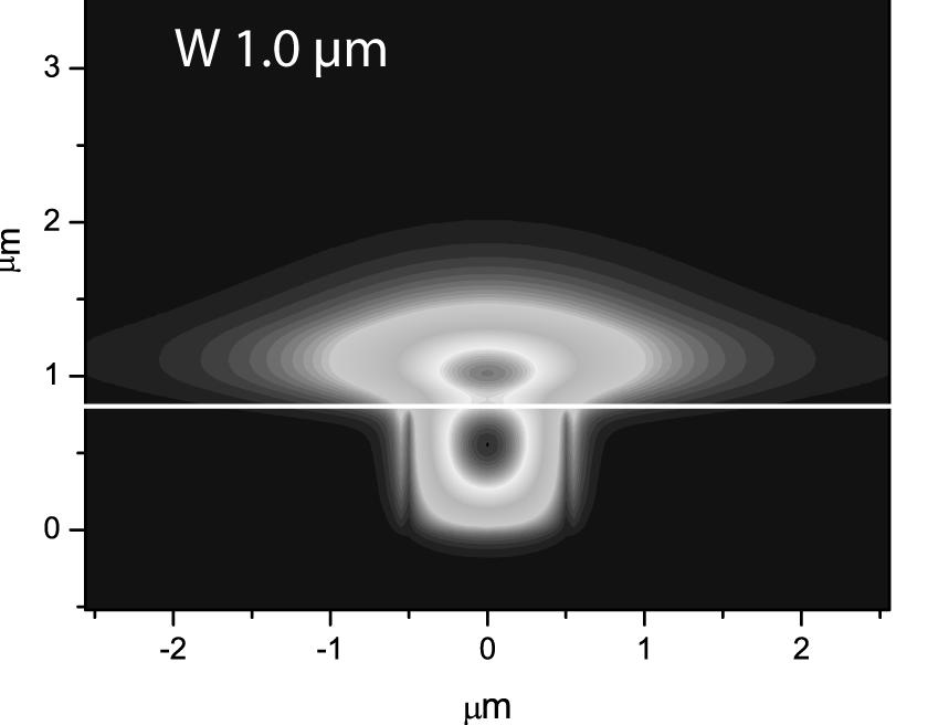
4 The vertical refractive index profile of the hybrid waveguide is shown in Fig. 2 (a) along with a cross-section of the mode profile. Strong coupling occurs between the silicon waveguide and the active region due to their similar refractive indices resulting in the formation of a hybrid mode which strongly overlaps both the silicon waveguide and the quantum wells in the III-V material. The overlap of the optical mode with the quantum well active region is a key device parameter as it dictates the modal gain for lasers and amplifiers, and the responsivity for hybrid photo-detectors. FIGURE 2 The epitaxial structure of the InP wafer is shown in Table 1. The 8 quantum well active region is bounded by the n-layers and the separate confinement heterostructure region. The SCH layer allows for an increase in the overlap of the quantum well region with the optical mode. The superlattice region is used to inhibit the propagation of defects from the bonded layer into the quantum well region [ 6 ]. TABLE 1 Fig. 3 plots the confinement factor of the optical mode in both the silicon and the quantum well portion of the hybrid waveguide as a function of the silicon waveguide width, for a silicon waveguide height of 0.76um. Decreasing the silicon waveguide width pushes the mode up into the quantum well region providing higher modal gain. Counteracting this benefit is the reduction of the silicon confinement factor which reduces the amount of coupling from the hybrid waveguide to passive, silicon only, waveguides on the same chip. The control of the quantum well confinement factor with lithographically defined waveguide width is a novel and flexible way to alter device performance across the photonic chip. FIGURE 3 3. Device fabrication Fabry-Perot lasers at 13xxnm [ 7 ] and 15xxnm [ 8 ] have been fabricated using this hybrid waveguide architecture as well as optical amplifiers [ 9 ], photodetectors [ 10 ] and ring lasers [ 11 ]. The generic device process flow is as follows. First waveguides are patterned on the (100) surface of an undoped SOI substrate with a 1 µm thick buried oxide layer using standard projection photolithography and Cl 2 /Ar/HBr- based plasma reactive ion etching. These waveguides may include passive components such as optical (de)multiplexers, or ring resonators or simply straight waveguides used to demonstrate Fabry-Perot lasers. Next the InP waferand the SOI wafer undergo a rigorous surface clean, oxygen plasma surface treatment, and wash in deionised water prior to bonding. During the plasma treatment a thin hydrophilic (<5nm) oxide layer is grown on the surface of each wafer which is then terminated by highly reactive polar hydroxyl groups during the deionised water dip. When the two wafers are subsequently placed together the hydroxyl groups form bridging bonds between the two surfaces resulting in weak spontaneous bonding of the two wafers. To enhance the strength of this spontaneous bond the wafer 4 / 23
5 are then placed in an annealing chamber at 300 C at a pressure of 2 MPa for 12 hours. This slow bake helps out diffusion of interface trapped molecules and activates the formation of stronger covalent bonds, resulting in stronger bonding of the two materials. After bonding the InP is patterned into mesa s; the N- and P-metals are deposited followed by proton implantation of the mesa to form a conductive channel in the center of the mesa through which current can flow. A typical hybrid silicon active cross-section is shown in Fig 1. More details of device fabrication are given in [ 7-11 ]. 4.1 Hybrid silicon Amplifiers A good example of the use of this novel platform is in the fabrication of an optical amplifier [ 9 ]. Currently the only silicon based amplifier has been demonstrated using the Raman Amplification [ 12 ]. Integration of InP quantum wells with the silicon waveguide allows electrically pumped gain compatible with silicon photonics. A SEM cross-section of the amplifier is shown in Fig. 4. The silicon strip waveguide height is 0.76um and its width is 2um. The total amplifier length is 1.36mm long. For these waveguide dimensions the overlap of the optical mode with the quantum wells is 3.4%. FIGURE 4 Devices were characterized by angle polishing (7 ) and AR-coating the facets and coupling the light into and out of the amplifier with lensed single mode fiber, with a measured coupling loss of -5dB. The amplifier gain as a function of bias current is shown in Fig. 5a. The maximum fiber-fiber gain for TE polarized light is 3dB corresponding to an on-chip gain of 13dB at a wavelength of 1575nm. Due to the compressive strain on the quantum wells these devices work predominantly on TE polarization with only 1dB on-chip gain for TM polarization. Fig. 5b shows the on-chip gain as a function of chip output power, the 3-dB output saturation power is 11dBm which is higher than centered quantum well optical amplifiers due to the reduced mode overlap with the off-center, evanescently-coupled, quantum wells. FIGURE Hybrid silicon lasers Of course demonstrating net gain allows one to fabricate a laser. Both Fabry-Perot and ring lasers have demonstrated using this hybrid platform, at both 1.3xxum and 1.5xxum wavelength. Fabry-Perot lasers have been fabricated from hybrid waveguides polished to a length of 850um [ 7, 8 ]. Again coupling from the laser was done using lensed fiber with a coupling loss of 6dB to the hybrid waveguides with silicon dimensions of 2.5um, 0.76um and for the silicon strip waveguide width and height. The mode overlap with the silicon waveguide and quantum wells is calculated to be 75% and 3% respectively. The hybrid waveguide facets were polished to give ~ 30% reflectivity end mirrors. The L-I curves for the light coupling to the single mode optical fiber is shown in Fig. 6. The laser threshold is 65mA at a temperature of 15 C. The laser emits light up to a temperature of 40 C and taking into account the 6dB coupling loss and that light is only 5 / 23
6 collected from one side of the laser the total maximum power emitted is 14mW corresponding to a differential efficiency of 12.7%. FIGURE Hybrid silicon photodetectors The same basic device architecture that is used to fabricate lasers can also be used to fabricate hybrid silicon photodetectors when the quantum wells are operated under reverse bias [ 10 ]. The device schematic and SEM are shown in Fig. 7a and b. The 400um long hybrid photo-detector is coupled to a 100um long passive silicon waveguide. The mesa at the interface is angled at 7 to reduce the reflection at the passive/active device junction. The silicon rib waveguide dimensions are 0.5um, 0.69um and 0.19um for the width, waveguide height and slab height. The mode overlap with the silicon waveguide and quantum wells is calculated to be 74% and 3.4% respectively. FIGURE 7 The responsivity of the detector was measured by coupling TE light into the silicon waveguide. Fig. 8 shows the photodetector s external responsivity as a function of wavelength. Taking into account the -5.5dB coupling loss into the detector the device has a relatively flat responsivity of 1.13 A/W from nm at 3.0V, this corresponds to an internal quantum efficiency of ~ 90%. Again due to the compressive strain in the quantum wells TM responsivity is much lower and measured at 0.23A/W. The frequency response of the detector was measured using a network analyzer to be 470MHz. Currently this is limited by the large capacitance of the long device and can be scaled up to 10GHz with a responsivity of 60% by reducing the device length and width. FIGURE Integrated hybrid silicon chip In general ring lasers suffer from bi-directional lasing, that is lasing occurs in the clockwise and anti-clockwise direction in the ring [ 13 ]. Coupling between the degenerate clockwise and anti-clockwise modes results in instability and kinks in the L-I curve of the single sided laser output, see for example the dotted grey curve in Fig. 10. One way to force unidirectional lasing is to seed the cavity in the preferred direction with an external light source. Here we integrate an ASE seed with the ring laser to obtain unidirectional lasing and an on-chip power monitor to ease device testing using the hybrid silicon platform. The ring laser is fabricated with silicon waveguide of width, height, and slab height of 1.65 µm, 0.69 µm and 0.19 µm respectively. The calculated overlap of the optical mode with the silicon waveguides is 64 % while there is a 4.2 % overlap in the quantum wells. The radius of curvature of the ring resonator is 100um, and the evanescent couplers are fabricating of two 100um long waveguides placed 0.6um apart. This coupler corresponds to 85% of light being fed back into the ring. The ASE source and power monitor were both fabricated from a straight hybrid waveguide with a 400um length. Reverse biasing a section resulted in it being a photo-detector, forward biasing it allowed it to emit 6 / 23
7 spontaneous radiation and act as an ASE source. A schematic and top-down SEM of the integrated circuit is shown in Fig. 9. FIGURE 9 The responsivity of the photodetectors was measured by dicing and polishing a discrete detector in the same chip and launching laser light into the detector through a lensed fiber. The fiber coupled responsivity was measured to be 0.25 A/W at 1580nm. Taking into consideration the ~30% reflection off the waveguide facet and an estimated /-.25 db coupling loss, we estimate the photodetector responsivity to be in the range of A/W. This corresponds to a quantum efficiency between 97%-86%. We use a responsivity of 1.25 A/W in the remainder of this section such that the laser power values are on the conservative side. The detector dark current was measured to be 200 µa. Fig. 10 shows the LI curve for the ring laser with different biases being applied to the ASE seed. With no seed bias the ring laser output is very erratic due to mode hopping as the laser output switches between clockwise and anticlockwise lasing as the laser bias is varied. At 75mA forward detector current, this LI becomes smoother, and at 100 ma, the anticlockwise propagating mode achieves stable unidirectional lasing. The laser runs continuous mode with a maximum output power of the ring laser is 2mW, with a threshold of 150mA. FIGURE 10 Fig. 11 shows the measured multi-mode lasing spectrum of the laser driven at 240 ma. The lasing wavelength is nm with a 0.21 nm mode spacing corresponding to a group index of FIGURE Wafer level processing The experiments run so far have been fabricated using die to die bonding of 8x8mm 2 InP die. To scale this processing up to whole SOI wafer level there are two basic approaches to consider: 1) Wafer to wafer bonding: here bonding would be done using whole InP wafers, which has the advantage that the surface treatment and bonding is done on a complete III-V wafer easing the handling. Disadvantages include the disparity between commercially available SOI and InP wafers. 12-inch SOI wafers are readily available whereas InP wafers are only now becoming available at 6-inch size, although at high cost. Obviously this disparity in size of the available wafers reduces the attractiveness of this approach as it does not allow the full usage, and hence economics of the large SOI wafers. 2) Given that a significant amount of the III-V wafer will be etched away during device fabrication a better approach might be bonding multiple III-V die to an SOI wafer. This has the key advantage that scaling can be done to any SOI wafer size irrespective of the III-V wafer availability, and the III-V die size can be set to efficiently use the InP material. All this comes at the cost of processing complexity, as 7 / 23
8 every die needs to undergo its own surface treatment before bonding, followed by rough alignment of the die to SOI wafer. However, in general the economic advantages of being able to buy smaller III-V wafers to process large SOI wafers makes this approach more attractive. 6. Conclusion The hybrid silicon platform is described which can be used to integrated III-V optoelectronic components with silicon photonics. The novelty of this approach lies in the wafer scale fabrication it opens up for lasers and other active devices on a silicon platform. Amplifiers with 13dB on-chip gain, photo-detectors with 90% quantum efficiency and lasers with output powers of 14mW are described. As proof of the integration potential of this platform a unidirectional laser is presented by integrating an ASE seed with a ring laser and on-chip power monitor. This wafer scale approach to integration of active components onto silicon will enable optical interconnects around PC s and servers where their current price is too expensive. 8 / 23
9 Acknowledgements This work was supported by DARPA through contracts W911NF and W911NF , and by Intel. The authors thank Jag Shah, Mike Haney, Matt Sysak, Ying-Hao Kuo, Di Liang, Brian Koch and Emily Burmeister for useful discussions and K. Callegari and G. Zeng for sample preparation. 9 / 23
10 References 1 G. T. Reed, & A. P. Knights, Silicon Photonics: An Introduction, John Wiley, Chichester, West Sussex, (2004). 2 L.Pavesi, & D. J. Lockwood, (eds.), Silicon Photonics, Springer-Verlag, Berlin, (2004). 3 S. Bidnyk, D. Feng, A. Balakrishnam, M. Pearson, M. Gao, H. Liang, W. Qian, C-C Kung, J. Fong, J. Yin and M. Ashgari, Phot. Tech. Lett. 18 (22), pp (2006) 4 A. Liu, L. Liao, D. Rubin, H. Nguyen, B. Ciftcioglu, Y. Chetrit, N. Izhaky, and M. Paniccia, Opt. Express 15, (2007) 5 M. Morse, O. Dosunmu, G. Sarid, and Y. Chetrit Phot. Tech. Lett. 18 (23), (2006). 6 A. Karim, K. A. Black, P. Abraham, D. Lofgreen,Y. J. Chiu, J. Piprek, J. E. Bowers Phot. Tech. Lett. 12 (11) (2000) 7 H-H Chang, A. W. Fang, M. N. Sysak, H. Park, R. Jones, O. Cohen, O. Raday, M. J. Paniccia, and J. E. Bowers, 1310nm Silicon Evanescent Laser, submitted for publication 8 A. W. Fang, H. Park, O. Cohen, R. Jones, M. J. Paniccia, and J. E. Bowers, Opt. Express 14, (2006) 9 H. Park, A. W. Fang, O. Cohen, R. Jones, M. J. Paniccia, and J. E. Bowers, Phot. Tech. Lett. 19 (4), (2007) 10 H. Park, A. W. Fang, R. Jones, O. Cohen, O. Raday, M. N. Sysak, M. J. Paniccia, and J. E. Bowers, Opt. Express 15 (10), pp (2007) 11 A. W. Fang, R. Jones, H. Park, O. Cohen, O. Raday, M. J. Paniccia, and J. E. Bowers, Opt. Express 15 (5) pp , (2007) 12 R. Jones, H. Rong, A. Liu, A. Fang, M. Paniccia, D. Hak, and O. Cohen, Opt. Express 13, (2005) 13 J. P. Hohimer and G. A. Vawter, Appl. Phys. Lett. 63 (18) (1993) 10 / 23
11 Figure Captions Figure 1: Schematic cross-section of the hybrid silicon laser. Figure 2: (a) Vertical refractive index profile of hybrid silicon waveguide and mode profile; (b) 2D mode profiles of hybrid silicon waveguide with width 1.0um and 2.5um Figure 3: Confinement factor of mode with quantum well and silicon region as a function of silicon waveguide width. Figure 4: SEM cross-section of hybrid silicon optical amplifier Figure 5: (a) Hybrid silicon amplifier gain versus bias current and (b) gain versus output power Figure 6: L-I curve for hybrid silicon laser Figure 7: (a) Schematic and (b) cross-section SEM of hybrid silicon photo-detector Figure 8: Responsivity as a function of wavelength for bias voltages between 0 and 3.0V Figure 9: (a) Schematic and (b) top down SEM of ring laser integrated with ASE seed and power monitor Figure 10: L-I curve for ring laser as for 0; 50; 75 and 100mA bias on ASE seed. Figure 11: lasing spectrum of ring laser Table 1: Epitaxial structure of InP wafer 11 / 23
12 y Fig.1 12 / 23

13 Fig 2a Fig 2b 13 / 23
14 0.8 Confinement Factors Width (um) QWs Silicon Fig 3 14 / 23
15 Fig 4 15 / 23
16 Fig 5a Fig 5b 16 / 23
17 Fig.6 17 / 23


18 Fig 7a mesa SOI waveguide Fig 7b 18 / 23
19 Fig 8 19 / 23
20 ASE seed Fig 9a Laser ASE seed Power Monitor Fig 9b 20 / 23
21 ma 50 ma 75 ma 100 ma Laser power (mw) Current (ma) Fig / 23
22 Fig / 23
23 Table / 23
Integrated AlGaInAs-silicon evanescent racetrack laser and photodetector
 Integrated AlGaInAs-silicon evanescent racetrack laser and photodetector Alexander W. Fang 1, Richard Jones 2, Hyundai Park 1, Oded Cohen 3, Omri Raday 3, Mario J. Paniccia 2, and John E. Bowers 1 1 University
Heterogeneous Integration of Silicon and AlGaInAs for a Silicon Evanescent Laser
 Invited Paper Heterogeneous Integration of Silicon and AlGaInAs for a Silicon Evanescent Laser Alexander W. Fang a, Hyundai Park a, Richard Jones b, Oded Cohen c, Mario J. Paniccia b, and John E. Bowers
Hybrid silicon evanescent devices
 Hybrid silicon evanescent devices Si photonics as an integration platform has recently been a focus of optoelectronics research because of the promise of low-cost manufacturing based on the ubiquitous
Invited Paper. Keywords: Silicon evanescent laser, Silicon photonics, integration, photodetector, semiconductor laser
 Invited Paper Integrated AlGaInAs-silicon evanescent racetrack laser and photodetector Alexander W. Fang 1, Richard Jones 2, Hyundai Park 1, Oded Cohen 3, Omri Raday 3, Mario J. Paniccia 2, & John E. Bowers
Integrated AlGaInAs-silicon evanescent racetrack laser and photodetector
 Invited Paper Integrated AlGaInAs-silicon evanescent racetrack laser and photodetector Alexander W. Fang 1, Richard Jones 2, Hyundai Park 1, Oded Cohen 3, Omri Raday 3, Mario J. Paniccia 2, & John E. Bowers
Low threshold continuous wave Raman silicon laser
 NATURE PHOTONICS, VOL. 1, APRIL, 2007 Low threshold continuous wave Raman silicon laser HAISHENG RONG 1 *, SHENGBO XU 1, YING-HAO KUO 1, VANESSA SIH 1, ODED COHEN 2, OMRI RADAY 2 AND MARIO PANICCIA 1 1:
Electrically pumped hybrid AlGaInAs-silicon evanescent laser
 Electrically pumped hybrid AlGaInAs-silicon evanescent laser Alexander W. Fang 1, Hyundai Park 1, Oded Cohen 3, Richard Jones 2, Mario J. Paniccia 2, & John E. Bowers 1 1 University of California, Santa
A hybrid AlGaInAs-silicon evanescent waveguide photodetector
 A hybrid AlGaInAs-silicon evanescent waveguide photodetector Hyundai Park 1, Alexander W. Fang 1, Richard Jones 2, Oded Cohen 3, Omri Raday 3, Matthew N. Sysak 1, Mario J. Paniccia 2, and John E. Bowers
InP-based Waveguide Photodetector with Integrated Photon Multiplication
 InP-based Waveguide Photodetector with Integrated Photon Multiplication D.Pasquariello,J.Piprek,D.Lasaosa,andJ.E.Bowers Electrical and Computer Engineering Department University of California, Santa Barbara,
An integrated recirculating optical buffer
 An integrated recirculating optical buffer Hyundai Park, John P. Mack, Daniel J. Blumenthal, and John E. Bowers* University of California, Santa Barbara, Department of Electrical and Computer Engineering,
A hybrid AlGaInAs-silicon evanescent preamplifier and photodetector
 A hybrid AlGaInAs-silicon evanescent preamplifier and photodetector Hyundai Park 1, Ying-hao Kuo 1, Alexander W. Fang 1, Richard Jones 2, Oded Cohen 3, Mario J. Paniccia 2, and John E. Bowers 1 1 University
A silicon avalanche photodetector fabricated with standard CMOS technology with over 1 THz gain-bandwidth product
 A silicon avalanche photodetector fabricated with standard CMOS technology with over 1 THz gain-bandwidth product Myung-Jae Lee and Woo-Young Choi* Department of Electrical and Electronic Engineering,
High-efficiency, high-speed VCSELs with deep oxidation layers
 Manuscript for Review High-efficiency, high-speed VCSELs with deep oxidation layers Journal: Manuscript ID: Manuscript Type: Date Submitted by the Author: Complete List of Authors: Keywords: Electronics
Lecture: Integration of silicon photonics with electronics. Prepared by Jean-Marc FEDELI CEA-LETI
 Lecture: Integration of silicon photonics with electronics Prepared by Jean-Marc FEDELI CEA-LETI Context The goal is to give optical functionalities to electronics integrated circuit (EIC) The objectives
Index. Cambridge University Press Silicon Photonics Design Lukas Chrostowski and Michael Hochberg. Index.
 absorption, 69 active tuning, 234 alignment, 394 396 apodization, 164 applications, 7 automated optical probe station, 389 397 avalanche detector, 268 back reflection, 164 band structures, 30 bandwidth
HIGH-EFFICIENCY MQW ELECTROABSORPTION MODULATORS
 HIGH-EFFICIENCY MQW ELECTROABSORPTION MODULATORS J. Piprek, Y.-J. Chiu, S.-Z. Zhang (1), J. E. Bowers, C. Prott (2), and H. Hillmer (2) University of California, ECE Department, Santa Barbara, CA 93106
Physics of Waveguide Photodetectors with Integrated Amplification
 Physics of Waveguide Photodetectors with Integrated Amplification J. Piprek, D. Lasaosa, D. Pasquariello, and J. E. Bowers Electrical and Computer Engineering Department University of California, Santa
CHAPTER 2 POLARIZATION SPLITTER- ROTATOR BASED ON A DOUBLE- ETCHED DIRECTIONAL COUPLER
 CHAPTER 2 POLARIZATION SPLITTER- ROTATOR BASED ON A DOUBLE- ETCHED DIRECTIONAL COUPLER As we discussed in chapter 1, silicon photonics has received much attention in the last decade. The main reason is
InP-based Waveguide Photodetector with Integrated Photon Multiplication
 InP-based Waveguide Photodetector with Integrated Photon Multiplication D.Pasquariello,J.Piprek,D.Lasaosa,andJ.E.Bowers Electrical and Computer Engineering Department University of California, Santa Barbara,
A continuous-wave Raman silicon laser
 A continuous-wave Raman silicon laser Haisheng Rong, Richard Jones,.. - Intel Corporation Ultrafast Terahertz nanoelectronics Lab Jae-seok Kim 1 Contents 1. Abstract 2. Background I. Raman scattering II.
Silicon Photonics Photo-Detector Announcement. Mario Paniccia Intel Fellow Director, Photonics Technology Lab
 Silicon Photonics Photo-Detector Announcement Mario Paniccia Intel Fellow Director, Photonics Technology Lab Agenda Intel s Silicon Photonics Research 40G Modulator Recap 40G Photodetector Announcement
InP-based waveguide photodiodes heterogeneously integrated on silicon-oninsulator for photonic microwave generation
 InP-based waveguide photodiodes heterogeneously integrated on silicon-oninsulator for photonic microwave generation Andreas Beling, 1,* Allen S. Cross, 1 Molly Piels, 2 Jon Peters, 2 Qiugui Zhou, 1 John
Heinrich-Hertz-Institut Berlin
 NOVEMBER 24-26, ECOLE POLYTECHNIQUE, PALAISEAU OPTICAL COUPLING OF SOI WAVEGUIDES AND III-V PHOTODETECTORS Ludwig Moerl Heinrich-Hertz-Institut Berlin Photonic Components Dept. Institute for Telecommunications,,
Silicon Photonics Technology Platform To Advance The Development Of Optical Interconnects
 Silicon Photonics Technology Platform To Advance The Development Of Optical Interconnects By Mieke Van Bavel, science editor, imec, Belgium; Joris Van Campenhout, imec, Belgium; Wim Bogaerts, imec s associated
Silicon Photonics Michael R. Bynum Physics 464: Applied Optics Winter 2006
 Silicon Photonics Michael R. Bynum Physics 464: Applied Optics Winter 2006 Abstract Copper interconnects will soon be the limiting factor of the performance of a computer. The aim of Silicon Photonics
Lecture 4 INTEGRATED PHOTONICS
 Lecture 4 INTEGRATED PHOTONICS What is photonics? Photonic applications use the photon in the same way that electronic applications use the electron. Devices that run on light have a number of advantages
Review Article Photonic Integration on the Hybrid Silicon Evanescent Device Platform
 Advances in Optical Technologies Volume 8, Article ID 68978, 17 pages doi:1.1155/8/68978 Review Article Photonic Integration on the Hybrid Silicon Evanescent Device Platform Hyundai Park, 1 Alexander W.
Vertical p-i-n germanium photodetector with high external responsivity integrated with large core Si waveguides
 Vertical p-i-n germanium photodetector with high external responsivity integrated with large core Si waveguides Ning-Ning Feng* 1, Po Dong 1, Dawei Zheng 1, Shirong Liao 1, Hong Liang 1, Roshanak Shafiiha
Wavelength switching using multicavity semiconductor laser diodes
 Wavelength switching using multicavity semiconductor laser diodes A. P. Kanjamala and A. F. J. Levi Department of Electrical Engineering University of Southern California Los Angeles, California 989-1111
Heterogeneously Integrated Microwave Signal Generators with Narrow- Linewidth Lasers
 Heterogeneously Integrated Microwave Signal Generators with Narrow- Linewidth Lasers John E. Bowers, Jared Hulme, Tin Komljenovic, Mike Davenport and Chong Zhang Department of Electrical and Computer Engineering
Si and InP Integration in the HELIOS project
 Si and InP Integration in the HELIOS project J.M. Fedeli CEA-LETI, Grenoble ( France) ECOC 2009 1 Basic information about HELIOS HELIOS photonics ELectronics functional Integration on CMOS www.helios-project.eu
Fabrication of High-Speed Resonant Cavity Enhanced Schottky Photodiodes
 Fabrication of High-Speed Resonant Cavity Enhanced Schottky Photodiodes Abstract We report the fabrication and testing of a GaAs-based high-speed resonant cavity enhanced (RCE) Schottky photodiode. The
Introduction Fundamentals of laser Types of lasers Semiconductor lasers
 ECE 5368 Introduction Fundamentals of laser Types of lasers Semiconductor lasers Introduction Fundamentals of laser Types of lasers Semiconductor lasers How many types of lasers? Many many depending on
High-speed Ge photodetector monolithically integrated with large cross silicon-on-insulator waveguide
 [ APPLIED PHYSICS LETTERS ] High-speed Ge photodetector monolithically integrated with large cross silicon-on-insulator waveguide Dazeng Feng, Shirong Liao, Roshanak Shafiiha. etc Contents 1. Introduction
Vertical External Cavity Surface Emitting Laser
 Chapter 4 Optical-pumped Vertical External Cavity Surface Emitting Laser The booming laser techniques named VECSEL combine the flexibility of semiconductor band structure and advantages of solid-state
Semiconductor Optical Active Devices for Photonic Networks
 UDC 621.375.8:621.38:621.391.6 Semiconductor Optical Active Devices for Photonic Networks VKiyohide Wakao VHaruhisa Soda VYuji Kotaki (Manuscript received January 28, 1999) This paper describes recent
Optoelectronics ELEC-E3210
 Optoelectronics ELEC-E3210 Lecture 4 Spring 2016 Outline 1 Lateral confinement: index and gain guiding 2 Surface emitting lasers 3 DFB, DBR, and C3 lasers 4 Quantum well lasers 5 Mode locking P. Bhattacharya:
Demonstration of directly modulated silicon Raman laser
 Demonstration of directly modulated silicon Raman laser Ozdal Boyraz and Bahram Jalali Optoelectronic Circuits and Systems Laboratory University of California, Los Angeles Los Angeles, CA 995-1594 jalali@ucla.edu
Applications of Cladding Stress Induced Effects for Advanced Polarization Control in Silicon Photonics
 PIERS ONLINE, VOL. 3, NO. 3, 27 329 Applications of Cladding Stress Induced Effects for Advanced Polarization Control in licon Photonics D.-X. Xu, P. Cheben, A. Delâge, S. Janz, B. Lamontagne, M.-J. Picard
The Past, Present, and Future of Silicon Photonics
 The Past, Present, and Future of Silicon Photonics Myung-Jae Lee High-Speed Circuits & Systems Lab. Dept. of Electrical and Electronic Engineering Yonsei University Outline Introduction A glance at history
Compact hybrid TM-pass polarizer for silicon-on-insulator platform
 Compact hybrid TM-pass polarizer for silicon-on-insulator platform Muhammad Alam,* J. Stewart Aitchsion, and Mohammad Mojahedi Department of Electrical and Computer Engineering, University of Toronto,
Examination Optoelectronic Communication Technology. April 11, Name: Student ID number: OCT1 1: OCT 2: OCT 3: OCT 4: Total: Grade:
 Examination Optoelectronic Communication Technology April, 26 Name: Student ID number: OCT : OCT 2: OCT 3: OCT 4: Total: Grade: Declaration of Consent I hereby agree to have my exam results published on
64 Channel Flip-Chip Mounted Selectively Oxidized GaAs VCSEL Array
 64 Channel Flip-Chip Mounted Selectively Oxidized GaAs VCSEL Array 69 64 Channel Flip-Chip Mounted Selectively Oxidized GaAs VCSEL Array Roland Jäger and Christian Jung We have designed and fabricated
Low Thermal Resistance Flip-Chip Bonding of 850nm 2-D VCSEL Arrays Capable of 10 Gbit/s/ch Operation
 Low Thermal Resistance Flip-Chip Bonding of 85nm -D VCSEL Arrays Capable of 1 Gbit/s/ch Operation Hendrik Roscher In 3, our well established technology of flip-chip mounted -D 85 nm backside-emitting VCSEL
SUPPLEMENTARY INFORMATION
 Room-temperature continuous-wave electrically injected InGaN-based laser directly grown on Si Authors: Yi Sun 1,2, Kun Zhou 1, Qian Sun 1 *, Jianping Liu 1, Meixin Feng 1, Zengcheng Li 1, Yu Zhou 1, Liqun
An electrically pumped germanium laser
 An electrically pumped germanium laser The MIT Faculty has made this article openly available. Please share how this access benefits you. Your story matters. Citation As Published Publisher Camacho-Aguilera,
IEEE JOURNAL OF SELECTED TOPICS IN QUANTUM ELECTRONICS 2010 Silicon Photonic Circuits: On-CMOS Integration, Fiber Optical Coupling, and Packaging
 IEEE JOURNAL OF SELECTED TOPICS IN QUANTUM ELECTRONICS 2010 Silicon Photonic Circuits: On-CMOS Integration, Fiber Optical Coupling, and Packaging Christophe Kopp, St ephane Bernab e, Badhise Ben Bakir,
High Speed pin Photodetector with Ultra-Wide Spectral Responses
 High Speed pin Photodetector with Ultra-Wide Spectral Responses C. Tam, C-J Chiang, M. Cao, M. Chen, M. Wong, A. Vazquez, J. Poon, K. Aihara, A. Chen, J. Frei, C. D. Johns, Ibrahim Kimukin, Achyut K. Dutta
Photonic crystal lasers in InGaAsP on a SiO 2 /Si substrate and its thermal impedance
 Photonic crystal lasers in InGaAsP on a SiO 2 /Si substrate and its thermal impedance M. H. Shih, Adam Mock, M. Bagheri, N.-K. Suh, S. Farrell, S.-J. Choi, J. D. O Brien, and P. D. Dapkus Department of
Silicon-On-Insulator based guided wave optical clock distribution
 Silicon-On-Insulator based guided wave optical clock distribution K. E. Moselund, P. Dainesi, and A. M. Ionescu Electronics Laboratory Swiss Federal Institute of Technology People and funding EPFL Project
Convergence Challenges of Photonics with Electronics
 Convergence Challenges of Photonics with Electronics Edward Palen, Ph.D., P.E. PalenSolutions - Optoelectronic Packaging Consulting www.palensolutions.com palensolutions@earthlink.net 415-850-8166 October
Integrated High Speed VCSELs for Bi-Directional Optical Interconnects
 Integrated High Speed VCSELs for Bi-Directional Optical Interconnects Volodymyr Lysak, Ki Soo Chang, Y ong Tak Lee (GIST, 1, Oryong-dong, Buk-gu, Gwangju 500-712, Korea, T el: +82-62-970-3129, Fax: +82-62-970-3128,
Realization of Polarization-Insensitive Optical Polymer Waveguide Devices
 644 Realization of Polarization-Insensitive Optical Polymer Waveguide Devices Kin Seng Chiang,* Sin Yip Cheng, Hau Ping Chan, Qing Liu, Kar Pong Lor, and Chi Kin Chow Department of Electronic Engineering,
On-chip Si-based Bragg cladding waveguide with high index contrast bilayers
 On-chip Si-based Bragg cladding waveguide with high index contrast bilayers Yasha Yi, Shoji Akiyama, Peter Bermel, Xiaoman Duan, and L. C. Kimerling Massachusetts Institute of Technology, 77 Massachusetts
Basic concepts. Optical Sources (b) Optical Sources (a) Requirements for light sources (b) Requirements for light sources (a)
 Optical Sources (a) Requirements for light sources (b) Requirements for light sources (a)") Optical Sources (a) Optical Sources (b) The main light sources used with fibre optic systems are: Light-emitting diodes (LEDs) Semiconductor lasers (diode lasers) Fibre laser and other compact solid-state
Optical Sources (a) Optical Sources (b) The main light sources used with fibre optic systems are: Light-emitting diodes (LEDs) Semiconductor lasers (diode lasers) Fibre laser and other compact solid-state
A 3.9 ns 8.9 mw 4 4 Silicon Photonic Switch Hybrid-Integrated with CMOS Driver
 A 3.9 ns 8.9 mw 4 4 Silicon Photonic Switch Hybrid-Integrated with CMOS Driver A. Rylyakov, C. Schow, B. Lee, W. Green, J. Van Campenhout, M. Yang, F. Doany, S. Assefa, C. Jahnes, J. Kash, Y. Vlasov IBM
NEXT GENERATION SILICON PHOTONICS FOR COMPUTING AND COMMUNICATION PHILIPPE ABSIL
 NEXT GENERATION SILICON PHOTONICS FOR COMPUTING AND COMMUNICATION PHILIPPE ABSIL OUTLINE Introduction Platform Overview Device Library Overview What s Next? Conclusion OUTLINE Introduction Platform Overview
Ultracompact Adiabatic Bi-sectional Tapered Coupler for the Si/III-V Heterogeneous Integration
 Ultracompact Adiabatic Bi-sectional Tapered Coupler for the Si/III-V Heterogeneous Integration Qiangsheng Huang, Jianxin Cheng 2, Liu Liu, 2, 2, 3,*, and Sailing He State Key Laboratory for Modern Optical
Optical MEMS in Compound Semiconductors Advanced Engineering Materials, Cal Poly, SLO November 16, 2007
 Optical MEMS in Compound Semiconductors Advanced Engineering Materials, Cal Poly, SLO November 16, 2007 Outline Brief Motivation Optical Processes in Semiconductors Reflectors and Optical Cavities Diode
Application Instruction 002. Superluminescent Light Emitting Diodes: Device Fundamentals and Reliability
 I. Introduction II. III. IV. SLED Fundamentals SLED Temperature Performance SLED and Optical Feedback V. Operation Stability, Reliability and Life VI. Summary InPhenix, Inc., 25 N. Mines Road, Livermore,
Optics Communications
 Optics Communications 283 (2010) 3678 3682 Contents lists available at ScienceDirect Optics Communications journal homepage: www.elsevier.com/locate/optcom Ultra-low-loss inverted taper coupler for silicon-on-insulator
Lecture 6 Fiber Optical Communication Lecture 6, Slide 1
 Lecture 6 Optical transmitters Photon processes in light matter interaction Lasers Lasing conditions The rate equations CW operation Modulation response Noise Light emitting diodes (LED) Power Modulation
Integrated Optoelectronic Chips for Bidirectional Optical Interconnection at Gbit/s Data Rates
 Bidirectional Optical Data Transmission 77 Integrated Optoelectronic Chips for Bidirectional Optical Interconnection at Gbit/s Data Rates Martin Stach and Alexander Kern We report on the fabrication and
Bistability in Bipolar Cascade VCSELs
 Bistability in Bipolar Cascade VCSELs Thomas Knödl Measurement results on the formation of bistability loops in the light versus current and current versus voltage characteristics of two-stage bipolar
SUPPLEMENTARY INFORMATION
 Transfer printing stacked nanomembrane lasers on silicon Hongjun Yang 1,3, Deyin Zhao 1, Santhad Chuwongin 1, Jung-Hun Seo 2, Weiquan Yang 1, Yichen Shuai 1, Jesper Berggren 4, Mattias Hammar 4, Zhenqiang
CMOS-compatible dual-output silicon modulator for analog signal processing
 CMOS-compatible dual-output silicon modulator for analog signal processing S. J. Spector 1*, M. W. Geis 1, G.-R.Zhou 2, M. E. Grein 1, F. Gan 2, M.A. Popović 2, J. U. Yoon 1, D. M. Lennon 1, E. P. Ippen
Integrated Focusing Photoresist Microlenses on AlGaAs Top-Emitting VCSELs
 Integrated Focusing Photoresist Microlenses on AlGaAs Top-Emitting VCSELs Andrea Kroner We present 85 nm wavelength top-emitting vertical-cavity surface-emitting lasers (VCSELs) with integrated photoresist
Microphotonics Readiness for Commercial CMOS Manufacturing. Marco Romagnoli
 Microphotonics Readiness for Commercial CMOS Manufacturing Marco Romagnoli MicroPhotonics Consortium meeting MIT, Cambridge October 15 th, 2012 Passive optical structures based on SOI technology Building
Ultralinear heterogeneously integrated ring-assisted Mach Zehnder interferometer modulator on silicon
 Research Article Vol. 3, No. 12 / December 2016 / Optica 1483 Ultralinear heterogeneously integrated ring-assisted Mach Zehnder interferometer modulator on silicon CHONG ZHANG, 1, *PAUL A. MORTON, 2 JACOB
Single-mode lasing in PT-symmetric microring resonators
 CREOL The College of Optics & Photonics Single-mode lasing in PT-symmetric microring resonators Matthias Heinrich 1, Hossein Hodaei 2, Mohammad-Ali Miri 2, Demetrios N. Christodoulides 2 & Mercedeh Khajavikhan
Semiconductor Optical Communication Components and Devices Lecture 18: Introduction to Diode Lasers - I
 Semiconductor Optical Communication Components and Devices Lecture 18: Introduction to Diode Lasers - I Prof. Utpal Das Professor, Department of lectrical ngineering, Laser Technology Program, Indian Institute
Hybrid vertical-cavity laser integration on silicon
 Invited Paper Hybrid vertical-cavity laser integration on Emanuel P. Haglund* a, Sulakshna Kumari b,c, Johan S. Gustavsson a, Erik Haglund a, Gunther Roelkens b,c, Roel G. Baets b,c, and Anders Larsson
Photonic Integrated Circuits Made in Berlin
 Fraunhofer Heinrich Hertz Institute Photonic Integrated Circuits Made in Berlin Photonic integration Workshop, Columbia University, NYC October 2015 Moritz Baier, Francisco M. Soares, Norbert Grote Fraunhofer
Semiconductor Devices
 Semiconductor Devices - 2014 Lecture Course Part of SS Module PY4P03 Dr. P. Stamenov School of Physics and CRANN, Trinity College, Dublin 2, Ireland Hilary Term, TCD 3 th of Feb 14 MOSFET Unmodified Channel
Performance of silicon micro ring modulator with an interleaved p-n junction for optical interconnects
 Indian Journal of Pure & Applied Physics Vol. 55, May 2017, pp. 363-367 Performance of silicon micro ring modulator with an interleaved p-n junction for optical interconnects Priyanka Goyal* & Gurjit Kaur
Multi-wavelength laser generation with Bismuthbased Erbium-doped fiber
 Multi-wavelength laser generation with Bismuthbased Erbium-doped fiber H. Ahmad 1, S. Shahi 1 and S. W. Harun 1,2* 1 Photonics Research Center, University of Malaya, 50603 Kuala Lumpur, Malaysia 2 Department
S-band gain-clamped grating-based erbiumdoped fiber amplifier by forward optical feedback technique
 S-band gain-clamped grating-based erbiumdoped fiber amplifier by forward optical feedback technique Chien-Hung Yeh 1, *, Ming-Ching Lin 3, Ting-Tsan Huang 2, Kuei-Chu Hsu 2 Cheng-Hao Ko 2, and Sien Chi
Compact Trench-Based Silicon-On-Insulator Rib Waveguide Ring Resonator With Large Free Spectral Range
 Brigham Young University BYU ScholarsArchive All Faculty Publications 2009-12-01 Compact Trench-Based Silicon-On-Insulator Rib Waveguide Ring Resonator With Large Free Spectral Range Seunghyun Kim Gregory
Electronic-Photonic ICs for Low Cost and Scalable Datacenter Solutions
 Electronic-Photonic ICs for Low Cost and Scalable Datacenter Solutions Christoph Theiss, Director Packaging Christoph.Theiss@sicoya.com 1 SEMICON Europe 2016, October 27 2016 Sicoya Overview Spin-off from
High brightness semiconductor lasers M.L. Osowski, W. Hu, R.M. Lammert, T. Liu, Y. Ma, S.W. Oh, C. Panja, P.T. Rudy, T. Stakelon and J.E.
 QPC Lasers, Inc. 2007 SPIE Photonics West Paper: Mon Jan 22, 2007, 1:20 pm, LASE Conference 6456, Session 3 High brightness semiconductor lasers M.L. Osowski, W. Hu, R.M. Lammert, T. Liu, Y. Ma, S.W. Oh,
Innovative ultra-broadband ubiquitous Wireless communications through terahertz transceivers ibrow
 Project Overview Innovative ultra-broadband ubiquitous Wireless communications through terahertz transceivers ibrow Mar-2017 Presentation outline Project key facts Motivation Project objectives Project
R. J. Jones Optical Sciences OPTI 511L Fall 2017
 R. J. Jones Optical Sciences OPTI 511L Fall 2017 Semiconductor Lasers (2 weeks) Semiconductor (diode) lasers are by far the most widely used lasers today. Their small size and properties of the light output
Robert G. Hunsperger. Integrated Optics. Theory and Technology. Sixth Edition. 4ü Spri rineer g<
 Robert G. Hunsperger Integrated Optics Theory and Technology Sixth Edition 4ü Spri rineer g< 1 Introduction 1 1.1 Advantages of Integrated Optics 2 1.1.1 Comparison of Optical Fibers with Other Interconnectors
Hybrid Integration Technology of Silicon Optical Waveguide and Electronic Circuit
 Hybrid Integration Technology of Silicon Optical Waveguide and Electronic Circuit Daisuke Shimura Kyoko Kotani Hiroyuki Takahashi Hideaki Okayama Hiroki Yaegashi Due to the proliferation of broadband services
OPTI510R: Photonics. Khanh Kieu College of Optical Sciences, University of Arizona Meinel building R.626
 OPTI510R: Photonics Khanh Kieu College of Optical Sciences, University of Arizona kkieu@optics.arizona.edu Meinel building R.626 Announcements Homework #3 is due today No class Monday, Feb 26 Pre-record
Department of Microelectronics, Faculty of Electrical Engineering, CTU, Prague Technicka 2, Prague 6, Czech Republic 2
 Ročník 2011 Číslo IV Design and Modeling of the ENR Polymer Microring Resonators Add/Drop Filter for Wavelength Division Multiplexing V. Prajzler 1, E. Strilek 1, I. Huttel 2, J. Spirkova 2, V. Jurka 3
High-Power Semiconductor Laser Amplifier for Free-Space Communication Systems
 64 Annual report 1998, Dept. of Optoelectronics, University of Ulm High-Power Semiconductor Laser Amplifier for Free-Space Communication Systems G. Jost High-power semiconductor laser amplifiers are interesting
Miniature Mid-Infrared Thermooptic Switch with Photonic Crystal Waveguide Based Silicon-on-Sapphire Mach Zehnder Interferometers
 Miniature Mid-Infrared Thermooptic Switch with Photonic Crystal Waveguide Based Silicon-on- Mach Zehnder Interferometers Yi Zou, 1,* Swapnajit Chakravarty, 2,* Chi-Jui Chung, 1 1, 2, * and Ray T. Chen
Near/Mid-Infrared Heterogeneous Si Photonics
 PHOTONICS RESEARCH GROUP Near/Mid-Infrared Heterogeneous Si Photonics Zhechao Wang, PhD Photonics Research Group Ghent University / imec, Belgium ICSI-9, Montreal PHOTONICS RESEARCH GROUP 1 Outline Ge-on-Si
High Power AlGaInAs/InP Widely Wavelength Tunable Laser
 Special Issue Optical Communication High Power AlGaInAs/InP Widely Wavelength Tunable Laser Norihiro Iwai* 1, Masaki Wakaba* 1, Kazuaki Kiyota* 3, Tatsuro Kurobe* 1, Go Kobayashi* 4, Tatsuya Kimoto* 3,
Design Rules for Silicon Photonics Prototyping
 Design Rules for licon Photonics Prototyping Version 1 (released February 2008) Introduction IME s Photonics Prototyping Service offers 248nm lithography based fabrication technology for passive licon-on-insulator
High speed silicon-based optoelectronic devices Delphine Marris-Morini Institut d Electronique Fondamentale, Université Paris Sud
 High speed silicon-based optoelectronic devices Delphine Marris-Morini Institut d Electronique Fondamentale, Université Paris Sud Data centers Optical telecommunications Environment Interconnects Silicon
Optical Amplifiers. Continued. Photonic Network By Dr. M H Zaidi
 Optical Amplifiers Continued EDFA Multi Stage Designs 1st Active Stage Co-pumped 2nd Active Stage Counter-pumped Input Signal Er 3+ Doped Fiber Er 3+ Doped Fiber Output Signal Optical Isolator Optical
Silicon Photonics Opportunity, applications & Recent Results
 Silicon Photonics Opportunity, applications & Recent Results Dr. Mario Paniccia Intel Fellow Director, Photonics Technology Lab Intel Corporation www.intel.com/go/sp Purdue University Oct 5 2007 Agenda
Optical Amplifiers Photonics and Integrated Optics (ELEC-E3240) Zhipei Sun Photonics Group Department of Micro- and Nanosciences Aalto University
 Zhipei Sun Photonics Group Department of Micro- and Nanosciences Aalto University") Photonics Group Department of Micro- and Nanosciences Aalto University Optical Amplifiers Photonics and Integrated Optics (ELEC-E3240) Zhipei Sun Last Lecture Topics Course introduction Ray optics & optical
Photonics Group Department of Micro- and Nanosciences Aalto University Optical Amplifiers Photonics and Integrated Optics (ELEC-E3240) Zhipei Sun Last Lecture Topics Course introduction Ray optics & optical
UC Santa Barbara UC Santa Barbara Previously Published Works
 UC Santa Barbara UC Santa Barbara Previously Published Works Title Compact broadband polarizer based on shallowly-etched silicon-on-insulator ridge optical waveguides Permalink https://escholarship.org/uc/item/959523wq
Figure 1 Basic waveguide structure
 Recent Progress in SOI Nanophotonic Waveguides D. Van Thourhout, P. Dumon, W. Bogaerts, G. Roelkens, D. Taillaert, G. Priem, R. Baets IMEC-Ghent University, Department of Information Technology, St. Pietersnieuwstraat
Wafer-scale 3D integration of silicon-on-insulator RF amplifiers
 Wafer-scale integration of silicon-on-insulator RF amplifiers The MIT Faculty has made this article openly available. Please share how this access benefits you. Your story matters. Citation As Published
Design and Simulation of Optical Power Splitter By using SOI Material
 J. Pure Appl. & Ind. Phys. Vol.3 (3), 193-197 (2013) Design and Simulation of Optical Power Splitter By using SOI Material NAGARAJU PENDAM * and C P VARDHANI 1 * Research Scholar, Department of Physics,
Spatial Investigation of Transverse Mode Turn-On Dynamics in VCSELs
 Spatial Investigation of Transverse Mode Turn-On Dynamics in VCSELs Safwat W.Z. Mahmoud Data transmission experiments with single-mode as well as multimode 85 nm VCSELs are carried out from a near-field