Process Technology to Fabricate High Performance MEMS on Top of Advanced LSI. Shuji Tanaka Tohoku University, Sendai, Japan
|
|
|
- Melvin Nelson
- 5 years ago
- Views:
Transcription
1 Process Technology to Fabricate High Performance MEMS on Top of Advanced LSI Shuji Tanaka Tohoku University, Sendai, Japan 1


2 JSAP Integrated MEMS Technology Roadmap More than Moore: Diversification More Moore: Miniaturization 3 µm 0.8 µm Integrated inertia sensors DMD Present High performance integrated sensors ~2015 Self-controlled one-chip sensors ~2020 Integrated health care devices Implantable devices One-chip multiband/ tunable wireless chips ~2025 Smaller More inteillent More distributed 2 Nanoelectronics


3 Multiband Wireless Communication GSM/PDC 800 MHz 900 MHz 1.9 GHz W-CDMA 1.92~1.98 GHz UL 2.11~2.17 GHZ DL PHS PHS 1.88~1.92 GHz W-LAN 5.16~5.35 GHz 2.4~2.48 GHz Digital TV TV 470~770 MHz WiMAX 2.5~2.7 GHz 4th 4th Gen. 3 Multi-band wireless communication chip for W- CDMA + GSM/GPRS/EDGE (Qualcomm, QSC6240) Tx Rx
4 Integration of Wireless Communication System Unimplemented system Frequency tuning circuit Rx Filter Mixer LNA 0/90 º A/D A/D Digital signal processor Discrete devices Integrated devices based on RF CMOS technology Real one-chip solution enables not only advanced mobile communication systems but also ubiquitous network sensors, wireless healthcare chips etc. 4 Integration of advanced LSI and mechanical devices (SAW/BAW filters, clock oscillators, RF MEMS switches, variable capacitors) is a key.

 G")


5 Inertia Sensors (Analog Devices) G sensor Detection circuit Safety steel ball sensor μm 1.3 μm 2 μm ADXRS150 2-axis gyro A tiny capacitance change (12 zf) corresponding to Å displacement is detectable by the embedded integrated circuit in the gyro.
 Poly Si sensor structure Judy et al.")


6 Integrated Accelerometer (Analog Devices) On-CMOS structure Circuit (NPN, NMOS) Poly Si sensor structure Judy et al., Hilton Head Island WS 2004, 27 Poly-Si sensor structure on 3 µm-ruled, W-metalized BiCMOS Poly-Si annealing at 1100 C for 30 min, Impossible to fabricate in LSI foundry SOI MEMS structure Sensor structure release Trench isolation from this trench Sensor structure Circuit SOI 6 Single crystal Si sensor structure beside 0.6 μm-ruled, Al-metalized CMOS Compatible with advanced LSI from LSI foundry, Low space efficiency


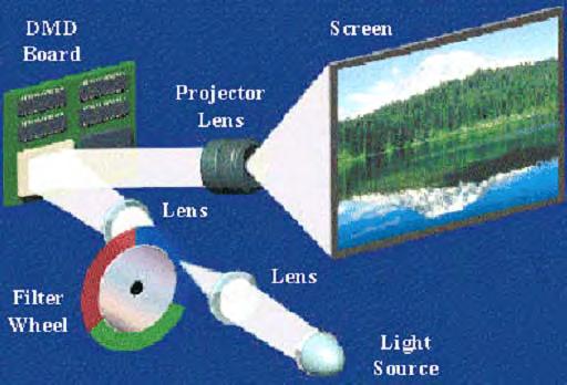
7 Digital Micromirror Device (TI) Hornbeck, IEDM 2007, ~16 μm square micromirrors ~2 μs response time 8.5 V driving voltage ±12 tilt angle = pixels for SVGA ~ = pixels for SXGA

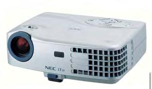

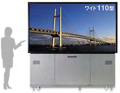
8 Applications of DMD Panasonic Rear-projection television NEC Weight: 1 kg 8 Mobile projector NEC Projector for cinema complex
 Resist 0.8 µm CMOS address 1.")
 Al SiO 2 Al Resist 5.")


 1687 4.")
9 Metal Surface Micromachining for DMD (TI) Resist 0.8 µm CMOS address 1. Sacrificial resist layer circuit (SRAM) Al SiO 2 Al Resist 5. Sacrificial resist layer and Al mirror 2. Al and SiO 2 mask for hinges SiO 2 Al 6. Sacrificial resist etching 3. Al and SiO 2 mask for beams 9 Kessel et al., Proc. IEEE, 86 (1998) Al etching for beams and hinges Hornbeck, IEDM 2007, 17-24

10 MEMS-LSI Integration using Ge Sacrificial Layer Multi-freq. AlN Lamb wave resonator monolithically integrated with LSI Application to one-chip high-speed communication devices Collaboration with NDK 1. Ge patterning and SiO 2 deposition Ge SiO 2 LSI 2. Metal patterning and AlN deposition Mo Al AlN 310 MHz LSI 3. AlN and Au/Cr patterning Au/Cr 4. Ge sacrificial etching μm
 Ni bridge 200 µm Ground Signal Off state Actuation pad Ground 11 Notches for close contact Sacrificial PR (3.5 µm) GND Signal Sacrificial PR (1.")
11 Electrostatic-Actuated Capacitive Shunt Switch On state Yuki et al., Sensor Symposium 2007 Dielectric layer(sio 2 ) Ni bridge 200 µm Ground Signal Off state Actuation pad Ground 11 Notches for close contact Sacrificial PR (3.5 µm) GND Signal Sacrificial PR (1.5 µm) GND Isolation (db) Driving voltage: 38 V Insert loss Isolation Freqency(GHz) Frequency (GHz) Insertion loss (db)
 12 Device wafer 3.")
12 Wafer-Level Packaging of RF MEMS Switch Yuki et al., Sensor Symposium 2007 Polyolefin mold Dry film resist 1. Molding dry film resist Exposed part 4. Developing and over-coating 2. Exposing dry film resist Exposed part CPW Cavity CPW Dry film resist DC in (Au/Cr) 12 Device wafer 3. Laminating molded dry film resist and exposing RF MEMS switch packaged by dry film resist

13 Phase Shifter Using RF MEMS Switches Switching line type Reflection type Z 0 Z 0 Z 1 Capacitive shunt SW Z 2 Capacitive shunt SW SW down Reflect here 13 Reflection-type phase shifter using RF MEMS switch (Taiko Denki & Tohoku Univ.) SW up Reflect here
 of bias voltage at which a half of mirrors land on the left side Test")
14 Memory Effect of Metal Hinges in DMD A. B. Southeimer, IEEE 40th Annual International Reliability Physics Symposium, Dallas, TX, 2002 Shift (%) of bias voltage at which a half of mirrors land on the left side Test duration Mirrors exhibiting hinge memory 50 % / 50% Duty cycle in accelerating test 5 % / 95% 14 Simulating random image Simulating static image
15 Wafer Bonding-based MEMS-LSI Integration 1. Preparation of a device layer on a support wafer Support wafer Interlayer e.g.) SiO 2, Polymer 2. Fabrication of a LSI wafer LSI wafer 3. Low temperature bonding of the device layer and the LSI wafer Adhesion layer Device layer e.g.) Single crystal Si, Piezoelectric materials, Diamond, Compound semiconductors Polymer 4. Removal of the support wafer/thinning of the device wafer LSI wafer 5. Fabrication of MEMS (e.g. RF MEMS switch, variable capacitor) or SAW/BAW devices Electrical connection 6. Release of the device by sacrificial etching 15


 ON (V drive = 8 V) 0")

16 Single Crystal RF MEMS Switch on Top of LSI Metal anchor Metal anchor OFF Signal line Actuation electrode Single crystal Si cantilever ON 200 μm Single crystal Si cantilever Metal anchor 16 Hight (μm) OFF (V drive = 0 V) ON (V drive = 8 V) Lateral length (μm) 200 μm Single crystal Si bridge RF MEMS switches on a dummy LSI wafer

17 Single-Crystal-Si-on-LSI (SOL) Technology 1. Fabrication of metal pads on a (dummy) LSI wafer LSI wafer 4. Patterning of metal electrodes 7. Removal of the photoresist molds 2. Bonding a SOI wafer on the LSI wafer using polymer interlayer SOI wafer 5. Shape formation of the device by reactive ion etching 8. Sacrificial polymer etching by O 2 ashing to release the device Polymer 3. Etching of the handle and BOX layers 6. Cu electroplating using photoresist molds for electrical connection Cu 17 Photoresist mold 200 μm

18 AlN/Si Composite Resonators on Top of LSI 1. Electrically-coupled AlN/Si composite thickness-mode filter 2. Mechanical-coupled AlN/Si composite disk array filter In Out In Out SiO 2 Si GND Si GND AlN Si AlN Si λ 4 Coupling Beam Out-of-phase mode In-phase mode 18 Collaboration with Mr. Matsumura (NiCT)


19 Single-Crystal-Si-on-LSI (SOL) Technology 1. Wafer bonding using polymer SOI wafer Polymer LSI 2. Handle layer and BOX layer etching 5. Metal patterning Al Au/Cr 6. Si etching Resist 3. Metal patterning Au/T Ru Au/Cr i 7. Sacrificial polymer etching 4. AlN deposition and patterning AlN SiO 2 19
20 AlN/Si Composite Resonators on Top of LSI Unpublished data 20


21 Share Wafer System in Tohoku University Shuttle service Given process Call for devices Registration from A corp., B univ. A B C D E F G H I A B Share wafer system Group A Sensor circuit Multiple devices in each shot Delivery after chip separation A B Group B Driver circuit Group C Oscillator circuit Is there a common process? Coordination with LSI foundry A D B C D A D C B C 21 Group D Actuator circuit Project members (NDA is concluded.) MEMS fabrication by each group Full wafers to each group
22 Summary There is strong demands for monolithic integration of advanced LSI and mechanical devices such as clock oscillators, mechanical filters, switches and sensors. More than Moore with Moore Moore and Biyond CMOS There are varieties of existing MEMS-LSI integration technology, but they are not suitable for the above applications. We have developed new versatile microprocess technology for the monolithic integration of high-performance MEMS on top of advanced LSI. Using the developed technology, we fabricated RF MEMS switches/variable capacitors, RF mechanical resonators and filters etc. 22 Acknowledgement: This study was partly supported by Special Coordination Funds for Promoting Science and Technology.
Surface Micromachining
 Surface Micromachining An IC-Compatible Sensor Technology Bernhard E. Boser Berkeley Sensor & Actuator Center Dept. of Electrical Engineering and Computer Sciences University of California, Berkeley Sensor
MEMS in ECE at CMU. Gary K. Fedder
 MEMS in ECE at CMU Gary K. Fedder Department of Electrical and Computer Engineering and The Robotics Institute Carnegie Mellon University Pittsburgh, PA 15213-3890 fedder@ece.cmu.edu http://www.ece.cmu.edu/~mems
CMP for More Than Moore
 2009 Levitronix Conference on CMP Gerfried Zwicker Fraunhofer Institute for Silicon Technology ISIT Itzehoe, Germany gerfried.zwicker@isit.fraunhofer.de Contents Moore s Law and More Than Moore Comparison:
RF MEMS for Low-Power Communications
 RF MEMS for Low-Power Communications Clark T.-C. Nguyen Center for Wireless Integrated Microsystems Dept. of Electrical Engineering and Computer Science University of Michigan Ann Arbor, Michigan 48109-2122
Study of MEMS Devices for Space Applications ~Study Status and Subject of RF-MEMS~
 Study of MEMS Devices for Space Applications ~Study Status and Subject of RF-MEMS~ The 26 th Microelectronics Workshop October, 2013 Maya Kato Electronic Devices and Materials Group Japan Aerospace Exploration
DEVELOPMENT OF RF MEMS SYSTEMS
 DEVELOPMENT OF RF MEMS SYSTEMS Ivan Puchades, Ph.D. Research Assistant Professor Electrical and Microelectronic Engineering Kate Gleason College of Engineering Rochester Institute of Technology 82 Lomb
High-yield Fabrication Methods for MEMS Tilt Mirror Array for Optical Switches
 : MEMS Device Technologies High-yield Fabrication Methods for MEMS Tilt Mirror Array for Optical Switches Joji Yamaguchi, Tomomi Sakata, Nobuhiro Shimoyama, Hiromu Ishii, Fusao Shimokawa, and Tsuyoshi
Micro Electro Mechanical System
 Micro Electro Mechanical System Jung-Mu Kim Mechatronics Mechatronics -The combination of mechanical engineering, electronic engineering and software engineering. Purpose of this interdisciplinary engineering
CMOS Digital Integrated Circuits Lec 2 Fabrication of MOSFETs
 CMOS Digital Integrated Circuits Lec 2 Fabrication of MOSFETs 1 CMOS Digital Integrated Circuits 3 rd Edition Categories of Materials Materials can be categorized into three main groups regarding their
EE C245 ME C218 Introduction to MEMS Design Fall 2007
 EE C245 ME C218 Introduction to MEMS Design Fall 2007 Prof. Clark T.-C. Nguyen Dept. of Electrical Engineering & Computer Sciences University of California at Berkeley Berkeley, CA 94720 Lecture 1: Definition
Transistor was first invented by William.B.Shockley, Walter Brattain and John Bardeen of Bell Labratories. In 1961, first IC was introduced.
 Unit 1 Basic MOS Technology Transistor was first invented by William.B.Shockley, Walter Brattain and John Bardeen of Bell Labratories. In 1961, first IC was introduced. Levels of Integration:- i) SSI:-
+1 (479)
") Introduction to VLSI Design http://csce.uark.edu +1 (479) 575-6043 yrpeng@uark.edu Invention of the Transistor Vacuum tubes ruled in first half of 20th century Large, expensive, power-hungry, unreliable
Introduction to VLSI Design http://csce.uark.edu +1 (479) 575-6043 yrpeng@uark.edu Invention of the Transistor Vacuum tubes ruled in first half of 20th century Large, expensive, power-hungry, unreliable
Final Exam Topics. IC Technology Advancement. Microelectronics Technology in the 21 st Century. Intel s 90 nm CMOS Technology. 14 nm CMOS Transistors
 ANNOUNCEMENTS Final Exam: When: Wednesday 12/10 12:30-3:30PM Where: 10 Evans (last names beginning A-R) 60 Evans (last names beginning S-Z) Comprehensive coverage of course material Closed book; 3 sheets
EE C245 ME C218 Introduction to MEMS Design
 EE C245 ME C218 Introduction to MEMS Design Fall 2008 Prof. Clark T.-C. Nguyen Dept. of Electrical Engineering & Computer Sciences University of California at Berkeley Berkeley, CA 94720 Lecture 1: Definition
Introduction to Microeletromechanical Systems (MEMS) Lecture 12 Topics. MEMS Overview
 Lecture 12 Topics. MEMS Overview") Introduction to Microeletromechanical Systems (MEMS) Lecture 2 Topics MEMS for Wireless Communication Components for Wireless Communication Mechanical/Electrical Systems Mechanical Resonators o Quality
Introduction to Microeletromechanical Systems (MEMS) Lecture 2 Topics MEMS for Wireless Communication Components for Wireless Communication Mechanical/Electrical Systems Mechanical Resonators o Quality
Industrialization of Micro-Electro-Mechanical Systems. Werner Weber Infineon Technologies
 Industrialization of Micro-Electro-Mechanical Systems Werner Weber Infineon Technologies Semiconductor-based MEMS market MEMS Market 2004 (total 22.7 BUS$) Others mostly Digital Light Projection IR Sensors
RF MEMS Simulation High Isolation CPW Shunt Switches
 RF MEMS Simulation High Isolation CPW Shunt Switches Authored by: Desmond Tan James Chow Ansoft Corporation Ansoft 2003 / Global Seminars: Delivering Performance Presentation #4 What s MEMS Micro-Electro-Mechanical
Lecture 020 ECE4430 Review II (1/5/04) Page 020-1
 Page 020-1") Lecture 020 ECE4430 Review II (1/5/04) Page 020-1 LECTURE 020 ECE 4430 REVIEW II (READING: GHLM - Chap. 2) Objective The objective of this presentation is: 1.) Identify the prerequisite material as taught
Lecture 020 ECE4430 Review II (1/5/04) Page 020-1 LECTURE 020 ECE 4430 REVIEW II (READING: GHLM - Chap. 2) Objective The objective of this presentation is: 1.) Identify the prerequisite material as taught
VLSI Design. Introduction
 VLSI Design Introduction Outline Introduction Silicon, pn-junctions and transistors A Brief History Operation of MOS Transistors CMOS circuits Fabrication steps for CMOS circuits Introduction Integrated
Electrostatically Tunable Analog Single Crystal Silicon Fringing-Field MEMS Varactors
 Purdue University Purdue e-pubs Birck and NCN Publications Birck Nanotechnology Center 2009 Electrostatically Tunable Analog Single Crystal Silicon Fringing-Field MEMS Varactors Joshua A. Small Purdue
Waveguide-Mounted RF MEMS for Tunable W-band Analog Type Phase Shifter
 Waveguide-Mounted RF MEMS for Tunable W-band Analog Type Phase Shifter D. PSYCHOGIOU 1, J. HESSELBARTH 1, Y. LI 2, S. KÜHNE 2, C. HIEROLD 2 1 Laboratory for Electromagnetic Fields and Microwave Electronics
Conference Paper Cantilever Beam Metal-Contact MEMS Switch
 Conference Papers in Engineering Volume 2013, Article ID 265709, 4 pages http://dx.doi.org/10.1155/2013/265709 Conference Paper Cantilever Beam Metal-Contact MEMS Switch Adel Saad Emhemmed and Abdulmagid
420 Intro to VLSI Design
 Dept of Electrical and Computer Engineering 420 Intro to VLSI Design Lecture 0: Course Introduction and Overview Valencia M. Joyner Spring 2005 Getting Started Syllabus About the Instructor Labs, Problem
RF(Radio Frequency) MEMS (Micro Electro Mechanical
 MEMS (Micro Electro Mechanical") Design and Analysis of Piezoelectrically Actuated RF-MEMS Switches using PZT and AlN PrashantTippimath M.Tech., Scholar, Dept of ECE M.S.Ramaiah Institute of Technology Bengaluru tippimathprashant@gmail.com
Design and Analysis of Piezoelectrically Actuated RF-MEMS Switches using PZT and AlN PrashantTippimath M.Tech., Scholar, Dept of ECE M.S.Ramaiah Institute of Technology Bengaluru tippimathprashant@gmail.com
Micromechanical Circuits for Wireless Communications
 Micromechanical Circuits for Wireless Communications Clark T.-C. Nguyen Center for Integrated Microsystems Dept. of Electrical Engineering and Computer Science University of Michigan Ann Arbor, Michigan
Lecture 0: Introduction
 Lecture 0: Introduction Introduction Integrated circuits: many transistors on one chip. Very Large Scale Integration (VLSI): bucketloads! Complementary Metal Oxide Semiconductor Fast, cheap, low power
Body-Biased Complementary Logic Implemented Using AlN Piezoelectric MEMS Switches
 University of Pennsylvania From the SelectedWorks of Nipun Sinha 29 Body-Biased Complementary Logic Implemented Using AlN Piezoelectric MEMS Switches Nipun Sinha, University of Pennsylvania Timothy S.
RF Micro/Nano Resonators for Signal Processing
 RF Micro/Nano Resonators for Signal Processing Roger T. Howe Depts. of EECS and ME Berkeley Sensor & Actuator Center University of California at Berkeley Outline FBARs vs. lateral bulk resonators Electrical
Micro- & Nano-technologies pour applications hyperfréquence à Thales Research &Technology Afshin Ziaei, Sébastien Demoustier, Eric Minoux
 Micro- & Nano-technologies pour applications hyperfréquence à Thales Research &Technology Afshin Ziaei, Sébastien Demoustier, Eric Minoux Outline Application hyperfréquence à THALES: Antenne à réseau réflecteur
An X band RF MEMS switch based on silicon-on-glass architecture
 Sādhanā Vol. 34, Part 4, August 2009, pp. 625 631. Printed in India An X band RF MEMS switch based on silicon-on-glass architecture M S GIRIDHAR, ASHWINI JAMBHALIKAR, J JOHN, R ISLAM, C L NAGENDRA and
MEMS for RF, Micro Optics and Scanning Probe Nanotechnology Applications
 MEMS for RF, Micro Optics and Scanning Probe Nanotechnology Applications Part I: RF Applications Introductions and Motivations What are RF MEMS? Example Devices RFIC RFIC consists of Active components
High Power RF MEMS Switch Technology
 High Power RF MEMS Switch Technology Invited Talk at 2005 SBMO/IEEE MTT-S International Conference on Microwave and Optoelectronics Conference Dr Jia-Sheng Hong Heriot-Watt University Edinburgh U.K. 1
New Type of RF Switches for Signal Frequencies of up to 75 GHz
 New Type of RF Switches for Signal Frequencies of up to 75 GHz Steffen Kurth Fraunhofer ENAS, Chemnitz, Germany Page 1 Contents Introduction and motivation RF MEMS technology Design and simulation Test
IWORID J. Schmitz page 1. Wafer-level CMOS post-processing Jurriaan Schmitz
 IWORID J. Schmitz page 1 Wafer-level CMOS post-processing Jurriaan Schmitz IWORID J. Schmitz page 2 Outline Introduction on wafer-level post-proc. CMOS: a smart, but fragile substrate Post-processing steps
EE C245 ME C218 Introduction to MEMS Design
 EE C245 ME C218 Introduction to MEMS Design Fall 2007 Prof. Clark T.-C. Nguyen Dept. of Electrical Engineering & Computer Sciences University of California at Berkeley Berkeley, CA 94720 Lecture 21: Gyros
Signal Integrity Design of TSV-Based 3D IC
 Signal Integrity Design of TSV-Based 3D IC October 24, 21 Joungho Kim at KAIST joungho@ee.kaist.ac.kr http://tera.kaist.ac.kr 1 Contents 1) Driving Forces of TSV based 3D IC 2) Signal Integrity Issues
Wafer-level Vacuum Packaged X and Y axis Gyroscope Using the Extended SBM Process for Ubiquitous Robot applications
 Proceedings of the 17th World Congress The International Federation of Automatic Control Wafer-level Vacuum Packaged X and Y axis Gyroscope Using the Extended SBM Process for Ubiquitous Robot applications
Low Actuation Wideband RF MEMS Shunt Capacitive Switch
 Available online at www.sciencedirect.com Procedia Engineering 29 (2012) 1292 1297 2012 International Workshop on Information and Electronics Engineering (IWIEE) Low Actuation Wideband RF MEMS Shunt Capacitive
MEMS Technologies and Devices for Single-Chip RF Front-Ends
 MEMS Technologies and Devices for Single-Chip RF Front-Ends Clark T.-C. Nguyen Dept. of Electrical Engineering & Computer Science University of Michigan Ann Arbor, Michigan 48105-2122 CCMT 06 April 25,
Chapter 3: Basics Semiconductor Devices and Processing 2006/9/27 1. Topics
 Chapter 3: Basics Semiconductor Devices and Processing 2006/9/27 1 Topics What is semiconductor Basic semiconductor devices Basics of IC processing CMOS technologies 2006/9/27 2 1 What is Semiconductor
Switch-less Dual-frequency Reconfigurable CMOS Oscillator using One Single Piezoelectric AlN MEMS Resonator with Co-existing S0 and S1 Lamb-wave Modes
 From the SelectedWorks of Chengjie Zuo January, 11 Switch-less Dual-frequency Reconfigurable CMOS Oscillator using One Single Piezoelectric AlN MEMS Resonator with Co-existing S and S1 Lamb-wave Modes
Chapter 3 Basics Semiconductor Devices and Processing
 Chapter 3 Basics Semiconductor Devices and Processing 1 Objectives Identify at least two semiconductor materials from the periodic table of elements List n-type and p-type dopants Describe a diode and
Power Reduction in RF
 Power Reduction in RF SoC Architecture using MEMS Eric Mercier 1 RF domain overview Technologies Piezoelectric materials Acoustic systems Ferroelectric materials Meta materials Magnetic materials RF MEMS
Micro-sensors - what happens when you make "classical" devices "small": MEMS devices and integrated bolometric IR detectors
 Micro-sensors - what happens when you make "classical" devices "small": MEMS devices and integrated bolometric IR detectors Dean P. Neikirk 1 MURI bio-ir sensors kick-off 6/16/98 Where are the targets
Jan Bogaerts imec
 imec 2007 1 Radiometric Performance Enhancement of APS 3 rd Microelectronic Presentation Days, Estec, March 7-8, 2007 Outline Introduction Backside illuminated APS detector Approach CMOS APS (readout)
EE C245 ME C218 Introduction to MEMS Design
 EE C45 ME C18 Introduction to MEMS Design Fall 008 Prof. Clark T.-C. Nguyen Dept. of Electrical Engineering & Computer Sciences University of California at Berkeley Berkeley, CA 9470 Lecture 7: Noise &
Optical Bus for Intra and Inter-chip Optical Interconnects
 Optical Bus for Intra and Inter-chip Optical Interconnects Xiaolong Wang Omega Optics Inc., Austin, TX Ray T. Chen University of Texas at Austin, Austin, TX Outline Perspective of Optical Backplane Bus
Piezoelectric Aluminum Nitride Micro Electromechanical System Resonator for RF Application
 Piezoelectric Aluminum Nitride Micro Electromechanical System Resonator for RF Application Prasanna P. Deshpande *, Pranali M. Talekar, Deepak G. Khushalani and Rajesh S. Pande Shri Ramdeobaba College
Sustaining the Si Revolution: From 3D Transistors to 3D Integration
 Sustaining the Si Revolution: From 3D Transistors to 3D Integration Tsu Jae King Liu Department of Electrical Engineering and Computer Sciences University of California, Berkeley, CA USA February 23, 2015
Wafer-scale 3D integration of silicon-on-insulator RF amplifiers
 Wafer-scale integration of silicon-on-insulator RF amplifiers The MIT Faculty has made this article openly available. Please share how this access benefits you. Your story matters. Citation As Published
EE4800 CMOS Digital IC Design & Analysis. Lecture 1 Introduction Zhuo Feng
 EE4800 CMOS Digital IC Design & Analysis Lecture 1 Introduction Zhuo Feng 1.1 Prof. Zhuo Feng Office: EERC 730 Phone: 487-3116 Email: zhuofeng@mtu.edu Class Website http://www.ece.mtu.edu/~zhuofeng/ee4800fall2010.html
3-5μm F-P Tunable Filter Array based on MEMS technology
 Journal of Physics: Conference Series 3-5μm F-P Tunable Filter Array based on MEMS technology To cite this article: Wei Xu et al 2011 J. Phys.: Conf. Ser. 276 012052 View the article online for updates
Topic 3. CMOS Fabrication Process
 Topic 3 CMOS Fabrication Process Peter Cheung Department of Electrical & Electronic Engineering Imperial College London URL: www.ee.ic.ac.uk/pcheung/ E-mail: p.cheung@ic.ac.uk Lecture 3-1 Layout of a Inverter
Integrated diodes. The forward voltage drop only slightly depends on the forward current. ELEKTRONIKOS ĮTAISAI
 1 Integrated diodes pn junctions of transistor structures can be used as integrated diodes. The choice of the junction is limited by the considerations of switching speed and breakdown voltage. The forward
Vertical Integration of MM-wave MMIC s and MEMS Antennas
 JOURNAL OF SEMICONDUCTOR TECHNOLOGY AND SCIENCE, VOL.6, NO.3, SEPTEMBER, 2006 169 Vertical Integration of MM-wave MMIC s and MEMS Antennas Youngwoo Kwon, Yong-Kweon Kim, Sanghyo Lee, and Jung-Mu Kim Abstract
RF DEVICES: BREAKTHROUGHS THANKS TO NEW MATERIALS. Jean-René Lequepeys. Leti Devices Workshop December 3, 2017
 RF DEVICES: BREAKTHROUGHS THANKS TO NEW MATERIALS Jean-René Lequepeys CELLULAR RF MARKETS RF cellular markets are still progressing Smartphones remain the main driver Declining growth rate but more complex
ITRS: RF and Analog/Mixed- Signal Technologies for Wireless Communications. Nick Krajewski CMPE /16/2005
 ITRS: RF and Analog/Mixed- Signal Technologies for Wireless Communications Nick Krajewski CMPE 640 11/16/2005 Introduction 4 Working Groups within Wireless Analog and Mixed Signal (0.8 10 GHz) (Covered
Piezoelectric Sensors and Actuators
 Piezoelectric Sensors and Actuators Outline Piezoelectricity Origin Polarization and depolarization Mathematical expression of piezoelectricity Piezoelectric coefficient matrix Cantilever piezoelectric
VLSI Design. Introduction
 Tassadaq Hussain VLSI Design Introduction Outcome of this course Problem Aims Objectives Outcomes Data Collection Theoretical Model Mathematical Model Validate Development Analysis and Observation Pseudo
Project: IEEE P Working Group for Wireless Personal Area Networks N
 Slide 1 Project: IEEE P802.15 Working Group for Wireless Personal Area Networks N (WPANs( WPANs) Title: [RF Devices for Millimeter-Wave Applications ] Date Submitted: [10 November 2003] Source: [Kenichi
A Novel WL-Integrated Low-Insertion-Loss Filter with Suspended High-Q Spiral Inductor and Patterned Ground Shields
 Progress In Electromagnetics Research C, Vol. 59, 41 49, 2015 A Novel WL-Integrated Low-Insertion-Loss Filter with Suspended High-Q Spiral Inductor and Patterned Ground Shields Tao Zheng 1, 2, Mei Han
On-chip 3D air core micro-inductor for high-frequency applications using deformation of sacrificial polymer
 header for SPIE use On-chip 3D air core micro-inductor for high-frequency applications using deformation of sacrificial polymer Nimit Chomnawang and Jeong-Bong Lee Department of Electrical and Computer
MEMS BASED QUARTZ OSCILLATORS and FILTERS for on-chip INTEGRATION
 MEMS BASED QUARTZ OSCILLATORS and FILTERS for on-chip INTEGRATION R. L. Kubena, F. P. Stratton, D. T. Chang, R. J. Joyce, and T. Y. Hsu Sensors and Materials Laboratory, HRL Laboratories, LLC Malibu, CA
SILICON BASED CAPACITIVE SENSORS FOR VIBRATION CONTROL
 SILICON BASED CAPACITIVE SENSORS FOR VIBRATION CONTROL Shailesh Kumar, A.K Meena, Monika Chaudhary & Amita Gupta* Solid State Physics Laboratory, Timarpur, Delhi-110054, India *Email: amita_gupta/sspl@ssplnet.org
EE C245 ME C218 Introduction to MEMS Design
 EE C245 ME C218 Introduction to MEMS Design Fall 2008 Prof. Clark T.-C. Nguyen Dept. of Electrical Engineering & Computer Sciences University of California at Berkeley Berkeley, CA 94720 Lecture 2: Benefits
FABRICATION OF CMOS INTEGRATED CIRCUITS. Dr. Mohammed M. Farag
 FABRICATION OF CMOS INTEGRATED CIRCUITS Dr. Mohammed M. Farag Outline Overview of CMOS Fabrication Processes The CMOS Fabrication Process Flow Design Rules Reference: Uyemura, John P. "Introduction to
This Week s Subject. DRAM & Flexible RRAM. p-channel MOSFET (PMOS) CMOS: Complementary Metal Oxide Semiconductor
 CMOS: Complementary Metal Oxide Semiconductor") DRAM & Flexible RRAM This Week s Subject p-channel MOSFET (PMOS) CMOS: Complementary Metal Oxide Semiconductor CMOS Logic Inverter NAND gate NOR gate CMOS Integration & Layout GaAs MESFET (JFET) 1 Flexible
DRAM & Flexible RRAM This Week s Subject p-channel MOSFET (PMOS) CMOS: Complementary Metal Oxide Semiconductor CMOS Logic Inverter NAND gate NOR gate CMOS Integration & Layout GaAs MESFET (JFET) 1 Flexible
Micro and Smart Systems
 Micro and Smart Systems Lecture - 39 (1)Packaging Pressure sensors (Continued from Lecture 38) (2)Micromachined Silicon Accelerometers Prof K.N.Bhat, ECE Department, IISc Bangalore email: knbhat@gmail.com
EE C245 ME C218 Introduction to MEMS Design
 EE C245 ME C218 Introduction to MEMS Design Fall 2007 Prof. Clark T.-C. Nguyen Dept. of Electrical Engineering & Computer Sciences University of California at Berkeley Berkeley, CA 94720 Lecture 20: Equivalent
3D SOI elements for System-on-Chip applications
 Advanced Materials Research Online: 2011-07-04 ISSN: 1662-8985, Vol. 276, pp 137-144 doi:10.4028/www.scientific.net/amr.276.137 2011 Trans Tech Publications, Switzerland 3D SOI elements for System-on-Chip
A Flexible Fabrication Process for RF MEMS Devices
 ROMANIAN JOURNAL OF INFORMATION SCIENCE AND TECHNOLOGY Volume 14, Number 3, 2011, 259 268 A Flexible Fabrication Process for RF MEMS Devices F. GIACOMOZZI, V. MULLONI, S. COLPO, J. IANNACCI, B. MARGESIN,
Compact Distributed Phase Shifters at X-Band Using BST
 Integrated Ferroelectrics, 56: 1087 1095, 2003 Copyright C Taylor & Francis Inc. ISSN: 1058-4587 print/ 1607-8489 online DOI: 10.1080/10584580390259623 Compact Distributed Phase Shifters at X-Band Using
Integration of AlN Micromechanical Contour- Mode Technology Filters with Three-Finger Dual Beam AlN MEMS Switches
 University of Pennsylvania From the SelectedWorks of Nipun Sinha 29 Integration of AlN Micromechanical Contour- Mode Technology Filters with Three-Finger Dual Beam AlN MEMS Switches Nipun Sinha, University
Design of MEMS Tunable Inductor Implemented on SOI and Glass wafers Using Bonding Technology
 Design of MEMS Tunable Inductor Implemented on SOI and Glass wafers Using Bonding Technology USAMA ZAGHLOUL* AMAL ZAKI* HAMED ELSIMARY* HANI GHALI** and HANI FIKRI** * Electronics Research Institute, **
MEMS Processes at CMP
 MEMS Processes at CMP MEMS Processes Bulk Micromachining MUMPs from MEMSCAP Teledyne DALSA MIDIS Micralyne MicraGEM-Si CEA/LETI Photonic Si-310 PHMP2M 2 Bulk micromachining on CMOS Compatible with electronics
Texas Instruments M Digital Micromirror Device (DMD)
") Texas Instruments 1910-612M Digital Micromirror Device (DMD) MEMS Process Review For comments, questions, or more information about this report, or for any additional technical needs concerning semiconductor
Texas Instruments 1910-612M Digital Micromirror Device (DMD) MEMS Process Review For comments, questions, or more information about this report, or for any additional technical needs concerning semiconductor
MEMS And Advanced Radar
 MEMS And Advanced Radar Dr. John K. Smith DARPA Tech 99: MEMS And Advanced Radar Page 1 Active ESA DARPA Tech 99: MEMS And Advanced Radar Page 2 T / R Module TX Controller Logic RX DARPA Tech 99: MEMS
Electrostatic actuation of silicon optomechanical resonators Suresh Sridaran and Sunil A. Bhave OxideMEMS Lab, Cornell University, Ithaca, NY, USA
 Electrostatic actuation of silicon optomechanical resonators Suresh Sridaran and Sunil A. Bhave OxideMEMS Lab, Cornell University, Ithaca, NY, USA Optomechanical systems offer one of the most sensitive
INF 5490 RF MEMS. LN12: RF MEMS inductors. Spring 2011, Oddvar Søråsen Department of informatics, UoO
 INF 5490 RF MEMS LN12: RF MEMS inductors Spring 2011, Oddvar Søråsen Department of informatics, UoO 1 Today s lecture What is an inductor? MEMS -implemented inductors Modeling Different types of RF MEMS
MICRO YAW RATE SENSORS
 1 MICRO YAW RATE SENSORS FIELD OF THE INVENTION This invention relates to micro yaw rate sensors suitable for measuring yaw rate around its sensing axis. More particularly, to micro yaw rate sensors fabricated
BROADBAND CAPACITIVE MICROMACHINED ULTRASONIC TRANSDUCERS RANGING
 BROADBAND CAPACITIVE MICROMACHINED ULTRASONIC TRANSDUCERS RANGING FROM 1 KHZ TO 6 MHZ FOR IMAGING ARRAYS AND MORE Arif S. Ergun, Yongli Huang, Ching-H. Cheng, Ömer Oralkan, Jeremy Johnson, Hemanth Jagannathan,
Lecture: Integration of silicon photonics with electronics. Prepared by Jean-Marc FEDELI CEA-LETI
 Lecture: Integration of silicon photonics with electronics Prepared by Jean-Marc FEDELI CEA-LETI Context The goal is to give optical functionalities to electronics integrated circuit (EIC) The objectives
Yoshihiko ISOBE Hiroshi MUTO Tsuyoshi FUKADA Seiji FUJINO
 Yoshihiko ISOBE Hiroshi MUTO Tsuyoshi FUKADA Seiji FUJINO Increased performance requirements in terms of the environment, safety and comfort have recently been imposed on automobiles to ensure efficient
PERSPECTIVES FOR DISRUPTIVE 200MM/8-INCH GAN POWER DEVICE AND GAN-IC TECHNOLOGY DR. DENIS MARCON SR. BUSINESS DEVELOPMENT MANAGER
 PERSPECTIVES FOR DISRUPTIVE 200MM/8-INCH GAN POWER DEVICE AND GAN-IC TECHNOLOGY DR. DENIS MARCON SR. BUSINESS DEVELOPMENT MANAGER What I will show you today 200mm/8-inch GaN-on-Si e-mode/normally-off technology
Sensors and actuators at NXP: bringing more than Moore to CMOS
 Sensors and actuators at NXP: bringing more than Moore to CMOS Joost van Beek Senior Principal Scientist Corporate R&D, NXP Semiconductors Presented at the International Symposium on Advanced Hybrid Nano
Electronic-Photonic ICs for Low Cost and Scalable Datacenter Solutions
 Electronic-Photonic ICs for Low Cost and Scalable Datacenter Solutions Christoph Theiss, Director Packaging Christoph.Theiss@sicoya.com 1 SEMICON Europe 2016, October 27 2016 Sicoya Overview Spin-off from
SAMPLE SLIDES & COURSE OUTLINE. Core Competency In Semiconductor Technology: 2. FABRICATION. Dr. Theodore (Ted) Dellin
 Dellin") & Digging Deeper Devices, Fabrication & Reliability For More Info:.com or email Dellin@ieee.org SAMPLE SLIDES & COURSE OUTLINE In : 2. A Easy, Effective, of How Devices Are.. Recommended for everyone who
& Digging Deeper Devices, Fabrication & Reliability For More Info:.com or email Dellin@ieee.org SAMPLE SLIDES & COURSE OUTLINE In : 2. A Easy, Effective, of How Devices Are.. Recommended for everyone who
Conjoined Rectangular Beam Shaped RF Micro-Electro- Mechanical System Switch for Wireless Applications
 International Journal of Advances in Microwave Technology (IJAMT) Vol.1, No.1, May 2016 10 Conjoined Rectangular Beam Shaped RF Micro-Electro- Mechanical System Switch for Wireless Applications R.Raman
EE 5611 Introduction to Microelectronic Technologies Fall Thursday, September 04, 2014 Lecture 02
 EE 5611 Introduction to Microelectronic Technologies Fall 2014 Thursday, September 04, 2014 Lecture 02 1 Lecture Outline Review on semiconductor materials Review on microelectronic devices Example of microelectronic
EE C245 ME C218 Introduction to MEMS Design Fall 2010
 Instructor: Prof. Clark T.-C. Nguyen EE C245 ME C218 Introduction to MEMS Design Fall 2010 Prof. Clark T.-C. Nguyen Dept. of Electrical Engineering & Computer Sciences University of California at Berkeley
CHAPTER 2 RF MEMS BASICS. 2.1 Switches for Microwave Applications
 CHAPTER 2 RF MEMS BASICS This chapter provides the basic introduction to RF MEMS switches. RF MEMS have in general seen a remarkable growth in the past two decades due to the immense potentials in defense
Aspemyr, Lars; Jacobsson, Harald; Bao, Mingquan; Sjöland, Henrik; Ferndal, Mattias; Carchon, G
 A 15 GHz and a 2 GHz low noise amplifier in 9 nm RF CMOS Aspemyr, Lars; Jacobsson, Harald; Bao, Mingquan; Sjöland, Henrik; Ferndal, Mattias; Carchon, G Published in: Topical Meeting on Silicon Monolithic
High-performance and Low-cost Capacitive Switches for RF Applications
 High-performance and Low-cost Capacitive Switches for RF Applications Bruce Liu University of California at Santa Barbara Toyon Research Corporation Toyon Research Corporation Fame Outline Motivation for
Design of Metal MUMPs based LLC Resonant Converter for On-chip Power Supplies
 Design of Metal MUMPs based LLC Resonant Converter for On-chip Power Supplies Fahimullah Khan, a, Yong Zhu,, b Junwei Lu,,c,Dzung Dao,,d Queensland Micro & Nanotechnology Centre Griffith University, Nathan,
A Low-cost Through Via Interconnection for ISM WLP
 A Low-cost Through Via Interconnection for ISM WLP Jingli Yuan, Won-Kyu Jeung, Chang-Hyun Lim, Seung-Wook Park, Young-Do Kweon, Sung Yi To cite this version: Jingli Yuan, Won-Kyu Jeung, Chang-Hyun Lim,
Lecture Integrated circuits era
 Lecture 1 1.1 Integrated circuits era Transistor was first invented by William.B.Shockley, Walter Brattain and John Bardeen of Bell laboratories. In 1961, first IC was introduced. Levels of Integration:-
Introduction to Microdevices and Microsystems
 PHYS 534 (Fall 2008) Module on Microsystems & Microfabrication Lecture 1 Introduction to Microdevices and Microsystems Srikar Vengallatore, McGill University 1 Introduction to Microsystems Outline of Lecture
Low noise THz NbN HEB mixers for radio astronomy: Development at Chalmers/ MC2
 Low noise THz NbN HEB mixers for radio astronomy: Development at Chalmers/ MC2 Sergey Cherednichenko Department of Microtechnology and Nanoscience, MC2 Chalmers University of Technology, SE-412 96, Gothenburg,
Low-Power VLSI. Seong-Ook Jung VLSI SYSTEM LAB, YONSEI University School of Electrical & Electronic Engineering
 Low-Power VLSI Seong-Ook Jung 2013. 5. 27. sjung@yonsei.ac.kr VLSI SYSTEM LAB, YONSEI University School of Electrical & Electronic Engineering Contents 1. Introduction 2. Power classification & Power performance