Dev Bhoomi Institute Of Technology Department of Electronics and Communication Engineering PRACTICAL INSTRUCTION SHEET REV. NO. : REV.
|
|
|
- Adela Fisher
- 5 years ago
- Views:
Transcription
1 Dev Bhoomi Institute Of Technology Department of Electronics and Communication Engineering PRACTICAL INSTRUCTION SHEET LABORATORY MANUAL EXPERIMENT NO. 1 ISSUE NO. : ISSUE DATE: July 2010 REV. NO. : REV. DATE : PAGE: 5 LABORATORY Name & Code: EDC LAB PEC-351 SEMESTER: III AIM:- FIELD EFFECT TRANSISTORS: - Single stage common source FET amplifier-plot of gain in db V s frequency, measurement of, bandwidth, input impedance, maximum signal handling capacity (MSHC) of an amplifier. EQUIPMENT REQUIRED:- S no. Particulars Specification/Range Quantity Make/Model No. 1. Trainer kit 1 2. Connecting wires 3. multimeter 1 4. CRO 1 CRO, Signal generator, Power Supply, Bread-board, Resistors (1MΩ, 4.7KΩ, 1KΩ), Capacitors (10μF, 100Μf), FET-BFW10 and connecting Wires. THEORY:- A JFET can be N-channel type or P-channel type. The structure of a P-channel JFET is similar to that of an N-channel JFET. Except that in its structure, N-type is replaced by P-type and P-type by N-type. The structure of an N-channel JFET is abar of N-type silicon. This bar behaves like a resistor between its two terminals, called source and drain. We introduce heavily doped P-type region on either side of bar. These P-regions are called gates. Usually two gates are connected together. This gate is used to control current flow from source to drain. This flow of electrons makes the drain current I d. The electrons in the bar pass through the space between the two P-regions. As width of this space between the p-regions can be controlled by varying gate voltage that is called a channel. We apply a small reverse bias to the gate. Because of the reverse bias, the width of depletion increases. Since the N-type bar is lightly doped compared to the P-regions, the depletions region extends more into the N-type bar. This reduced the width of the channel. Reduction in the width of the channel (the conductive portion of the bar) increases its resistance. This reduces the
2 drain current I d. There is one important point about the channel shape. It is narrower at the drain end. This happens because the amount of reveres bias is not same throughout the length of the P-N junction. When current flows through the bar, a potential drop occurs across its length. As a result the reverse bias between the gate and the drain end of the bar is more than that between the gate and the source end of the bar. The width of depletion region is more at the drain end than at the source end. As a result, the channel becomes narrower at the drain end. If the reverse gate bias is increased further, the channel becomes narrower at the drain end and drain current further reduces. If the reverse bias is made sufficiently large, the depletion region will extend into channel. This pinches off all current flow. The gate-source voltage at which pinch-off occurs is called PINCH-OFF voltage V p. PROCEDURE:- (1) Connect the circuit as per the circuit diagram. (2) Apply V i = 10 mv and V dd = +20v. (3) Now vary the frequency of the input signal and measure the corresponding amplitude variation in output at different values frequency. Note down the readings and plot the graph between gain and frequency. This curve is known as frequency response curve OBSERVATIONS:- S. NO INPUT VOLTAGE INPUT FREQUENCY OUTPUT VOLTAGE GAIN (V i ) (F i ) (V o ) (db)
3 RESULT:- Thus we have plotted a graph between gain and frequency to obtain a frequency response curve. The values of f L and f H from graph are given as F H = F L = BW = F H - F L PRECAUTIONS:- (1) All connections should be right and tight. (2) Readings should be taken carefully. (3) Scale on the graph should be taken correctly and carefully. PRE EXPERIMENTAL QUESTIONS: Q. Define FET. A. The field-effect transistor (FET) is a transistor that uses an electric field to control the shape and hence the conductivity of a channel of one type of charge carrier in a semiconductor material. FETs are sometimes called unipolar transistors to contrast their single-carrier-type operation with the dual-carrier-type operation of bipolar (junction) transistors (BJT). The concept of the FET predates the BJT, though it was not physically implemented until after BJTs due to the limitations of semiconductor materials and the relative ease of manufacturing BJTs compared to FETs at the time. Q. What are different terminals of FET? A. The FET's three terminals are: Source (S), through which the majority carriers enter the channel. Conventional current entering the channel at S is designated by I S. Drain (D), through which the majority carriers leave the channel. Conventional current entering the channel at D is designated by I D. Drain to Source voltage is V DS. Gate (G), the terminal that modulates the channel conductivity. By applying voltage to G, one can control I D
4 POST EXPERIMENTAL QUESTIONS: Q. What are advantages of the FET. A. The main advantage of the FET is its high input resistance, on the order of 100M ohms or more. Thus, it is a voltage-controlled device, and shows a high degree of isolation between input and output. It is a unipolar device, depending only upon majority current flow. It is less noisy and is thus found in FM tuners for quiet reception. It is relatively immune to radiation. It exhibits no offset voltage at zero drain current and hence makes an excellent signal chopper. It typically has better thermal stability than a BJT. Q. What are disadvantages of the FET? A. It has relatively low gain-bandwidth product compared to a BJT. The MOSFET has a drawback of being very susceptible to overload voltages, thus requiring special handling during installation. Q. What are the various applications of FET? A. Applications are in switching internal combustion engine ignition coils, where fast switching and voltage blocking capabilities are important. The most commonly used FET is the MOSFET. The CMOS (complementary metal oxide semiconductor) process technology is the basis for modern digital integrated circuits. This process technology uses an arrangement where the (usually "enhancement-mode") p-channel MOSFET and n-channel MOSFET are connected in series such that when one is on, the other is off.


5 Single Stage RC Coupled FET Amplifier Frequency Response
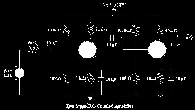
6 Dev Bhoomi Institute Of Technology Department of Electronics and Communication Engineering PRACTICAL INSTRUCTION SHEET LABORATORY MANUAL EXPERIMENT NO. 2 ISSUE NO. : ISSUE DATE: July 2010 REV. NO. : REV. DATE : PAGE: 6 LABORATORY Name & Code: EDC LAB PEC-351 SEMESTER: III AIM :- Bipolar transistor:- Designing of single stage RC coupled amplifier-design of DC biasing circuit using potential divider arrangement plot of frequency V s gain in db. Measurement of bandwidth of an amplifier, input impedance and Maximum signal Handing Capacity of an amplifier. APPARATUS:- S no. Particulars Specification/Range Quantity Make/Model No. 1. Trainer kit 1 2. Connecting wires 3. multimeter 1 4. CRO 1 CRO, Power supply, Signal Generator, Bread-board, Resistors, capacitors,transistor (BC 107) and connecting wires. Design of RC coupled amplifier (DC biasing circuit design) Design values: design a voltage divider circuit for given values: I C = 2mA R C = 2KΩ V CE = 4V V CC = 10V Determine the values of R 1, R 2,and R E. Solution: Ic = β I B I B = Ic β I 1 = 10 X I B I 1 = VCC R 1 +R 2 V CE = V C -V E V CE = V CC -I C R C -I E R E (I C =I E )
7 V CE = V CC -I C (R C +R E ) Ic = V B -V BE R E V B =I C X R E V B = R 2 X V CC R 1 +R 2 THEORY: Almost no electronic system can work without an amplifier. The voice of a single person could reach everybody in a hall only because of the amplification of the signal picked up by the P.A system. After a transistor is biased in the active region, it can work as an amplifier. We apply an ac voltage between the base and emitter terminals to produce fluctuations in the collector current.an amplified output signal is obtained when this fluctuating collector current flows through a collector resistor R c.when the input signal is so weak as to produce small fluctuations in the collector current compared to its quiescent value, the amplifier is called small signal amplifier (also voltage amplifier ). Such an amplifier is used as the first stage of the amplifier used in receivers (radio and TV), tape recorders, and stereos and measuring instruments.the circuit of a single stage transistor amplifier is shown in fig. Almost all amplifiers use potential divider biasing circuit because the design of the circuit is simple and it provides good stabilization of the operating point. If this circuit is to amplify ac voltages, some more components must be added such as the circuit capacitors are added. The capacitor C C is called coupling capacitors. A coupling capacitor passes an ac signal from one side to another. The capacitor C E works as a bypass capacitor. It bypasses all the ac currents from the emitter to ground. The resistance R represents the resistance of whatever is connected at the output. To what extent an amplifier enlarges signal is expressed in terms of its voltage gain. The voltage gain of an amplifier is given as A V = output AC voltage / input AC voltage A V = V o /V i The other quantities of interest for a voltage amplifier are current gain (A i ) input impedance (z i ) and output impedance (z o ).The performance of an amplifier is judged by observing whether all frequency component of the signal are amplified equally well. The information is provided by its frequency response curve. This curve illustrates how the magnitude of voltage gain of the amplifier varies with the freq. of the input signal (sinusoidal). It can be plotted by measuring voltage gain of the amplifier
8 for different frequencies of sinusoidal voltage fed to its input. Fig shows the frequency response curve of the typical RC coupled amplifier. B.W = f 2 f 1 PROCEDURE:- (1) Connect the circuit as the cat. Diagram. (2) Apply V cc = +15V &set i/p voltage in mv. (3) Now vary the frequency of i/p voltage &Measure the corresponding amplitude variation in o/p at different values of i/p frequency. (4) Not down the reading and plot a graph between gain and frequency. The curve is known as frequency response curve. OBSERVATIONS:- S. NO Input Voltage (V i ) Input Frequency (f) Output Voltage (V O ) Gain A=20log 10 (V o /V i RESULT:- Thus we have plot a graph between gain and frequency. This curve is known as frequency response curve and values of f2 and f1 from graph are:- F H = F L = B.W = Z i =
9 Max signal handling capacity = PRECAUTIONS:- (1) All connection should be right & tight. (2) Readings should be taken carefully. (3) Scale on the graph should be taken correctly & carefully. Single Stage RC Coupled BJT Amplifier

10 Frequency Response PRE EXPERIMENTAL QUESTIONS: Q. Define transistor. A. A transistor is a semiconductor device used to amplify and switch electronic signals and electrical power. It is composed of a semiconductor material with at least three terminals for connection to an external circuit. Q. Describe the operation of transistor as switch. A. Transistors are commonly used as electronic switches, both for high-power applications such as switched-mode power supplies and for low-power applications such as logic gates. In a grounded-emitter transistor circuit, such as the light-switch circuit shown, as the base voltage rises, the base and collector current rise exponentially. The collector voltage drops because of the collector load resistance (in this example, the resistance of the light bulb). If the collector voltage were zero, the collector current would be limited only by the light bulb resistance and the supply voltage. The transistor is then said to be saturated - it will have a very small voltage from collector to emitter. Providing sufficient base drive current is a key problem in the use of bipolar transistors as switches. The transistor provides current gain, allowing a relatively large current in the collector to be switched by a much smaller current into the base terminal. The ratio of these currents varies depending on the type of transistor, and even for a particular type, varies depending on the collector current. In the example light-switch circuit shown, the resistor is chosen to provide enough base current to ensure the transistor will be saturated. In any switching circuit, values of input voltage would be chosen such that the output is either completely off, or completely on. The transistor is acting as a switch, and this type of operation is common in digital circuits where only "on" and "off" values are relevant.
11 POST EXPERIMENTALQUESTIONS: Q. Name the ternimals of the transistor. A. Emitter, Collector and Base. Q. Why BJT Call as bipolar device? A. Bipolar transistors are so named because their operation involves both electrons and holes, as opposed to unipolar transistors, such as field-effect transistors, in which only one carrier type is involved in charge flow. Although a small part of the transistor current is due to the flow of majority carriers, most of the transistor current is due to the flow of minority carriers and so BJTs are classified as minority-carrier devices. Q. Why BJT called as current controlled device? A. The collector emitter current can be viewed as being controlled by the base emitter current (current control), or by the base emitter voltage (voltage control). These views are related by the current voltage relation of the base emitter junction, which is just the usual exponential current voltage curve of a PN junction (diode) The physical explanation for collector current is the amount of minority-carrier charge in the base region. Detailed models of transistor action, such as the Gummel Poon model, account for the distribution of this charge explicitly to explain transistor behavior more exactly. The charge-control view easily handles photo-transistors, where minority carriers in the base region are created by the absorption of photons, and handles the dynamics of turn-off, or recovery time, which depends on charge in the base region recombining. However, since base charge is not a signal that is visible at the terminals, the current- and voltage-control views are usually used in circuit design and analysis.
12 Dev Bhoomi Institute Of Technology Department of Electronics and Communication Engineering PRACTICAL INSTRUCTION SHEET LABORATORY MANUAL EXPERIMENT NO. 3 ISSUE NO. : ISSUE DATE: July 2010 REV. NO. : REV. DATE : PAGE: 6 LABORATORY Name & Code: EDC LAB PEC-351 SEMESTER: III EXPERIMENT NO 5 AIM:- Two Stage Amplifiers: - Plot of frequency V s gain, Estimation of Q factor, bandwidth of an amplifier. APPARATUS:- S no. Particulars Specification/Range Quantity Make/Model No. 1. Trainer kit 1 2. Connecting wires 3. multimeter 1 4. CRO 1 C.R.O Power supply, Signal Connecting wires. Generator, Bread board, Resistors,Capacitors, transistors & THEORY:- Gain of a single transistor amplifier Stage is not sufficient & has two or more stages are usually connected in cascade to provide the desired gains me times cascading is done to achieve the correct I/P or O/P impedance for a specific application. Most Popular cascade amplifier is formed by cascading several CS amplifier Overall gain A = A1. A2 Where A1 & A2 are the gain of individual stages. PROCEDURE:- (1) Connect the circuit as per the ckt. Diagram. (2) Apply V DD =20v & set I/p voltage in mv. (3) Now vary the frequency of I/p & measure the corresponding amplitude variation in o/p at different values of I/p frequency. (4) Note down the reading and plot a graph between gain and frequency. The curve is known as frequency response curve.
13 OBSERVATION S. NO Input Voltage (V i ) Input Frequency (f) Output Voltage (V O ) Gain A=20log 10 (V o /V i RESULT:- Thus we have plot a graph between gain and frequency. This curve is known is frequency response curve and the values of f H and f L from graph are:- F H = F L = B.W = PRECAUTION :- (1) All connection should be right & tight. (2) Reading should be taken carefully. (3) Scale on the graph should be taken correctly & carefully.

14 CASCADE CS AMLPLIFIER FREQUENCY RESPONS
15 Dev Bhoomi Institute Of Technology Department of Electronics and Communication Engineering PRACTICAL INSTRUCTION SHEET LABORATORY MANUAL EXPERIMENT NO. 4 ISSUE NO. : ISSUE DATE: July 2010 REV. NO. : REV. DATE : PAGE: 6 LABORATORY Name & Code: EDC LAB PEC-351 SEMESTER: III AIM:- EXPERTMENT NO -6 Common Collector configuration-emitter follower (using Darlington Pair):-Gain and input impedance measurement of the circuit. APPARATUS REQUIRED: S no. Particulars Specification/Range Quantity Make/Model No. 1. Trainer kit 1 2. Connecting wires 3. multimeter 1 4. CRO 1 NV6542 trainer, Digital Multimeter (DMM), Multimeter probes, 2mm Patch chords, Mains cord. Theory: Emitter Follower (using Darlington Pair) In recent years, electronics have been integrated into motor speed drives and a variety of Switching-type power supplies. This means that standard discrete components needed to be altered to provide better characteristics.the need for the Darlington pair grew from the limitations of SCRs and triac-type thyristors. Thyristors control current by delaying the turn-on time. The later the pulse is applied to turn them on, the smaller the amount of current they will conduct during each cycle.on the other hand, a transistor uses variable current (0 to saturation), which provides an output current that will be a duplication of the input. This means the transistors will produce an analog signal when an analog signal is provided to its base. The simple bipolar transistor has several limitations including slow switching speeds, low gains, and larger power losses due to the switching process. A family of high-gain transistors called metal-oxide
16 semiconductor field effect transistors (MOSFETs) was produced to address the gain problem, but they did not have the capability of controlling larger currents, so the Darlington pair was designed.the Darlington pair can actually be two discrete transistors that are connected in the driver/output configuration, or they can be a single device that has the two transistors internally connected at the point where it was manufactured as a single package. In Darlington pairs, transistor collectors are tied together and the emitter of the first transistor is directly coupled to the base of the second transistor. The total gain, which is often 1000 or more, is the- product of the gain of the individual transistors. For large currents it is standard and good procedure to use a Darlington pair of transistors, rather than a single one, which effectively acts like a single transistor with β that is the product of the two βs of the individual transistors. Figure 32 shown below is a Darlington pair since the emitter current of Q1 is the base current for Q2; the Darlington pair has an overall current gain of β= β1β 2 ADVANTAGES: 1. The key advantage of the Darlington configuration is that the total current gain of the circuit equals the product of the current gain of two devices since its current gain is much higher 2. Darlington transistors are circuits that combine two bipolar transistors in a single device; hence, they require lesser space than configurations that use two discrete transistors. 3. Darlington connection can have very high input impedance and can produce very large outputs current. DISADVANTAGES: 1. The disadvantage is the larger saturation voltage compared to single transistor configurations. 2. Darlington transistor pairs have more phase shift at high frequencies and can become unstable with negative feedback more easily. 3. Darlington transistors also have a higher base-emitter voltage, which1s the sum of both base emitter voltages. APPLICATIONS: Darlington connections are used with voltage regulators and power amplifiers. PROCEDURE FOR CURRENT GAIN, INPUT IMPEDANCE : 1. Connect a patch cord across sockets +12V of DC power supply and +12V of Emitter follower amplifier section (refer to figure 36). 2. Connect +5V of DC power supply to V in 1 terminal of Emitter follower amplifier section.
17 3. Connect a patch cord between socket A and B of Emitter follower amplifier section. 4. Connect a patch cord between socket E and F. 5. Now set the digital multimeter s dial to DC voltage mode. 6. Now connect the multimeter through multimeter probes to A and G1. 7. Switch on the power supply. 8. Now measure the DC voltage between A and ground G1 using DMM. This will give value of dc voltage input V in to the transistor T1.Note it down. 9. Switch off the power supply. 10. Calculate the input current (Ii) by substituting the value in following equation I in = (V in1 -V in )/ Rs Where, Vin1 =5 V,Rs =100 KΩ,Vin =DC voltage measured in step Note down this value of input current Iin. 12. Calculate the input impedance (Zin) by following formula in step 10. Z in =V in / I i 13. Now remove the patch cord between sockets +5V and V in1 14. Also remove the patch cord between sockets A and B. Connect a patch cord between socket E and F. 15. Now connect +5V directly at the base terminal B of transistor T Remove the patch cord between socket E and F and connect a DMM through probes between the sockets E and F 17. Now set the digital multimeter s dial to DC current mode to measure the output DC Current, I out between the sockets E and F refer to figure). 18. Switch on the power supply. 19. Note down the value of output current I out displayed on the DMM s display. 20. Ratio of output current to input current gives the overall of Darlington pair. Calculate the ratio of output current to input current by following formula β= I out / I i 21. Individual of transistors can be calculated by considering the transistors having identical and using the formula β= β 1 x β 2 β 1 =β 2 = β
18 PROCEDURE FOR VOLTAGE GAIN: 1. Connect the Sockets 1 and 2 of Sine Wave Generator section to CRO channel CH1 through CRO probes 3. Switch on the power supply.using the Frequency control and Amplitude control knobs of the Sine Wave Generator section, set the input signal at 1Vp-p, 1 KHz sine wave signal and observe the same on CRO channel CH1. 4. Switch off the power supply. Remove the CRO probes. 5. Connect a patch cord across sockets +12V of DC power supply and +12V of Emitter follower amplifier section. 6. Connect a patch cord between points V in and 1 and another patch cord between sockets G1 and 2 in Emitter follower amplifier section. 7. Connect a patch cord between sockets B and D. 8. Connect another patch cord between sockets E and F. 9. Connect the Sockets V in and G Connect the Sockets V out and G Switch on the power supply. 12. Observe simultaneously the input waveform between points V in & G1 display and measure the amplitude of input waveform. It is V in. 13. Also observe the output waveform between points V out and G2 on CRO display and measure the amplitude of the output waveform. It is V out. 14. Calculate the voltage gain (it will be approximately equal to unity). CALCULATION: Av =Vout / Vin CURRENT GAIN, INPUT IMPEDANCE : I i = (V in -V in )/ Rs Z in = V in / I i β= I out / I i β= β 1 x β 2
19 VOLTAGE GAIN: Voltage Gain, Av = V out / V in Where, Vin = Input Voltage, Vout = Output Voltage RESULT: Current Gain of Darlington Pair, β = Individual β of transistor = β =... Input impedance of emitter follower = Ω Voltage gain of Darlington pair =..V Input Current Input Voltage, Vin = 4.40 V Iin = [Vin1 - Vin] / Rs Iin = [5-4.40] / 100 x 10 3 Iin = 6 μ A Input Impedance Zin = Vin/ Ii Zin = 4.40 / 6 x 10⁻⁶ Zin = 733 K Output Current Iout = 35.4 ma Current Gain of Darlington Pair β= Iout / Iin β= 35.4 ma / 6 μa β= 5900
20 Individual of transistor β1 = β2 = β = 76.8 Input Voltage Vin = 1 Vpp Output Voltage Vout == 1 Vpp Voltage gain of Darlington pair Av = Vout / Vin Av = 1 Vpp / 1Vpp Av = 1 Emitter Follower Amplifier using Darlington Pair
21 Dev Bhoomi Institute Of Technology Department of Electronics and Communication Engineering PRACTICAL INSTRUCTION SHEET LABORATORY MANUAL EXPERIMENT NO. 5 ISSUE NO. : ISSUE DATE: July 2010 REV. NO. : REV. DATE : PAGE: 4 LABORATORY Name & Code: EDC LAB PEC-351 SEMESTER: III AIM:- Oscillators:- Sinusoidal Oscillator (a) Wein bridge Oscillator (b) Phase shift Oscillator APPARATUS:- S no. Particulars Specification/Range Quantity Make/Model No. 1. Trainer kit 1 2. Connecting wires 3. multimeter 1 4. CRO 1 CRO,Power supply, Bread Board, IC 741, Resistor (3.3kΩ-2, 10kΩ), Capacitors (0.05Μf-2). THEORY:- The Wein-bridge Oscillator is a standard circuit for generating low frequency in the rang of 10 HZ to 1MHZ. It is used all commercial audio generator. Wein-bridge is a ac bridge which balances only at particular frequency called null frequency. When the bridge is balanced the output of bridge is zero. For Oscillations to be sustained the phase shift to through the coupling network must be zero. It can be shown that this condition occurs at a frequency given by F O = 1/2IIRC Here op-amp is used in non-inverting configuration and provides O o phase shift. Since input impedance is large and out put impedance is small for the OP-AMP, there is no loading on the feed back network. When the above condition is satisfied we must have β= 1/3 This means that amplifier must have a gain of at lest 3. The Phase Shift oscillator produces positive feed back by using an inverting amplifier and adding another of phase shift with the three high pass filter circuit. It produces this 180 o phase shift for only one frequency
22 β= 1/29 This means that amplifier must have a gain of at lest 29 PROCEDURE:- (1) Connect the circuit as per the diagram. on the breadboard. (2) Provide +/-12V Supply to the circuit. (3) Observe the output sine wave on the CRO. (4) Note the time period of this wave and calculate its frequency. Also calculate the gain. OBSERVATION:- 1. Calculate value of frequency of w.b. ocs. using the formula Wein-bridge F o = 1 2πRC 2.Calculate value of frequency of w.b. ocs. using the formula Wein-bridge F o = II RC 6 3. Practical Value of frequency as observed on CRO. RESULT:- 1. Thus we have measured the frequency and gain for sine wave generated by Weinbridge oscillator. PRECAUTION:- 1. All connections should be right and tight. 2. Readings should be taken carefully. 3. Power supply should be switched off after use.


23 Circuit diagram for wein bridge oscillator
24 Circuit diagram for phase shift oscillator
25 Dev Bhoomi Institute Of Technology Department of Electronics and Communication Engineering PRACTICAL INSTRUCTION SHEET LABORATORY MANUAL EXPERIMENT NO. 6(a) ISSUE NO. : ISSUE DATE: July 2010 REV. NO. : REV. DATE : PAGE: 2 LABORATORY Name & Code: EDC LAB PEC-351 SEMESTER: III COLPITTS OSCILLATOR AIM: To determine the frequency of oscillations of a given Colpitts Oscillator. APPARATUS: S.No Name Range / Value Quantity PROCEDURE: 1. DC Regulated Power Supply (0-30V) 1 2. Resistors 560, 47 K Each 1 4. Resistors 4.7 K 2 5. Capacitors 100 F, F Each 1 6. Decade Inductance Box Decade Capacitance Box CRO Connect the circuit diagram as shown in the figure. 2. Switch on the power supply. 3. Connect the out put terminals to CRO. 4. Adjust the capacitances until a sinusoidal wave form is observed on the CRO. 5. Measure the time period of the sinusoidal wave form (T) and determine the Frequency (1/T). 6. Repeat the above steps for different values of L, C 1 & C Tabulate the readings and compare with theoretical values CALCULATIONS: RESULT: f 0 (practical) =1/T Hz. f0 (theoretical) f 0 1. [Where C eq C 1 C 2 ] 2 LC eq C 1 C 2


26 TABULAR FORM: C ( F) Practical Theoretical S.NO. L (mh) frequency Frequency C 1 C 2 (Hz) (Hz) VIVA QUESTIONS: 1. Why RC network oscillator cannot be used at Radio frequencies? 2. Why LC network oscillators are preferred at high frequencies? 3. Why a buffer amplifier is required in between an oscillator and a load? 4. What is meant by ringing in an amplifier? 5. Why the crystal oscillator is highly stable? 6. Draw the electrical equivalent circuit of a crystal oscillato
27 Dev Bhoomi Institute Of Technology Department of Electronics and Communication Engineering PRACTICAL INSTRUCTION SHEET LABORATORY MANUAL EXPERIMENT NO. 6(b) ISSUE NO. : ISSUE DATE: July 2010 REV. NO. : REV. DATE : PAGE: 2 LABORATORY Name & Code: EDC LAB PEC-351 SEMESTER: III RC-PHASE SHIFT OSCILLATOR AIM : To determine the frequency of oscillations of a given RC phase shift Oscillator. APPARATUS: S.No Name Range / Value Quantity 1. DC Regulated power supply (0 30V) 1 2. Transistor BC Resistors 1K, 47K, 560 Each 1 4. Resistors 4.7K 4 5. Capacitors 0.1 F, 0.01 F, F Each 3 6. Capacitors F 1 7. Capacitors 100 F 20V 1 PROCEDURE: 1. Connect the circuit diagram as shown in the figure. 2. Switch on the power supply. 3. Connect the O/P terminals to C.R.O. 4. Observe the sinusoidal wave form on C.R.O. 5. Determine the time period (T) of the wave form and frequency (1/T). 6. Repeat the above procedure for different sets of Capacitors. 7. Tabulate the readings and compare with theoretical values. CALCULATIONS: RESULT: f (practical) = 1/T Hz. 1 f o (Theoretical) Where K = R C / R = 1. 2 RC 6 4K R 1 = R 2 = R 3 = R. C 1 = C 2 = C 3 = C.


28 TABULAR FORM: S.No Resistance Capacitance Practical Theoretical (K ) ( F) Frequency (Hz) Frequency (Hz) VIVA QUESTIONS: 1. Which type of feedback is incorporated in RC phase shift oscillator? 2. Can we built up an RC phase shift oscillator using two stages of RC network of each 90 0 phase shift? 3. State Barkhausen criterion? 4. What is the condition imposed on A and to get sustained oscillations?

 1 2.")
29 Dev Bhoomi Institute Of Technology Department of Electronics and Communication Engineering PRACTICAL INSTRUCTION SHEET LABORATORY MANUAL EXPERIMENT NO. 7 ISSUE NO. : ISSUE DATE: July 2010 REV. NO. : REV. DATE : PAGE: 2 LABORATORY Name & Code: EDC LAB PEC-351 SEMESTER: III AIM: To Determine the frequency of oscillations of a Hartley Oscillator and compare it with the theoretical values. APPARATUS: S.No Name Range / Value Quantity 1. D.C Regulated Power Supply (0 30V) 1 2. Resistors 1KΩ, 10kΩ, 47KΩ Each 1 3. Capacitors 0.22µF 2 4. Decade Capacitance Box Decade Inductance Box CRO -- 1
30 PROCEDURE: 1. Connect the circuit as shown in the figure. 2. Connect the O / P of the oscillator to the C.R.O. 3. Adjust the Capacitance and Inductance Boxes until a sinusoidal signal is observed in the CRO. 4. Determine the frequency of the wave form. 5. Determine the frequency by varying the capacitance in convenient steps. 6. Tabulate the readings and compare the readings with the theoretical values. FORMULAS: Theoretical Frequency f L eq C Practical Frequency F: 1 T CALCULATIONS: RESULT: Capacitance C ( F ) Inductance ( m H ) L 1 L 2 Practical Frequency (Hz) Theoretical Frequency (Hz) VIVA QUESTIONS: 1. Why RC network oscillator cannot be used at Radio frequencies? 2. Why LC network oscillators are preferred at high frequencies? 3. Why a buffer amplifier is required in between an oscillator and a load? 4. What is meant by ringing in an amplifier? 5. Why the crystal oscillator is highly stable? 6. Draw the electrical equivalent circuit of a crystal oscillator?
ANALOG ELECTRONIC CIRCUITS LABORATORY MANUAL (CODE: EEE - 228)
") ANALOG ELECTRONIC CIRCUITS LABORATORY MANUAL (CODE: EEE - 228) DEPARTMENT OF ELECTRONICS & COMMUNICATION ENGINEERING ANIL NEERUKONDA INSTITUTE OF TECHNOLOGY & SCIENCES (Affiliated to AU, Approved by AICTE
ANALOG ELECTRONIC CIRCUITS LABORATORY MANUAL (CODE: EEE - 228) DEPARTMENT OF ELECTRONICS & COMMUNICATION ENGINEERING ANIL NEERUKONDA INSTITUTE OF TECHNOLOGY & SCIENCES (Affiliated to AU, Approved by AICTE
Unit III FET and its Applications. 2 Marks Questions and Answers
 Unit III FET and its Applications 2 Marks Questions and Answers 1. Why do you call FET as field effect transistor? The name field effect is derived from the fact that the current is controlled by an electric
Lab 4 : Transistor Oscillators
 Objective: Lab 4 : Transistor Oscillators In this lab, you will learn how to design and implement a colpitts oscillator. In part II you will implement a RC phase shift oscillator Hardware Required : Pre
Document Name: Electronic Circuits Lab. Facebook: Twitter:
 Document Name: Electronic Circuits Lab www.vidyathiplus.in Facebook: www.facebook.com/vidyarthiplus Twitter: www.twitter.com/vidyarthiplus Copyright 2011-2015 Vidyarthiplus.in (VP Group) Page 1 CIRCUIT
EXPT NO: 1.A. COMMON EMITTER AMPLIFIER (Software) PRELAB:
 PRELAB:") EXPT NO: 1.A COMMON EMITTER AMPLIFIER (Software) PRELAB: 1. Study the operation and working principle of CE amplifier. 2. Identify all the formulae you will need in this Lab. 3. Study the procedure of
EXPT NO: 1.A COMMON EMITTER AMPLIFIER (Software) PRELAB: 1. Study the operation and working principle of CE amplifier. 2. Identify all the formulae you will need in this Lab. 3. Study the procedure of
Shankersinh Vaghela Bapu Institute of Technology INDEX
 Shankersinh Vaghela Bapu Institute of Technology Diploma EE Semester III 3330905: ELECTRONIC COMPONENTS AND CIRCUITS INDEX Sr. No. Title Page Date Sign Grade 1 Obtain I-V characteristic of Diode. 2 To
FREQUENTLY ASKED QUESTIONS
 FREQUENTLY ASKED QUESTIONS UNIT-1 SUBJECT : ELECTRONIC DEVICES AND CIRCUITS SUBJECT CODE : EC6202 BRANCH: EEE PART -A 1. What is meant by diffusion current in a semi conductor? (APR/MAY 2010, 2011, NOV/DEC
Dev Bhoomi Institute Of Technology Department of Electronics and Communication Engineering PRACTICAL INSTRUCTION SHEET
 Dev Bhoomi Institute Of Technology Department of Electronics and Communication Engineering PRACTICAL INSTRUCTION SHEET LABORATORY MANUAL EXPERIMENT NO. ISSUE NO. : ISSUE DATE: REV. NO. : REV. DATE : PAGE:
Dev Bhoomi Institute Of Technology Department of Electronics and Communication Engineering PRACTICAL INSTRUCTION SHEET REV. NO. : REV.
 Dev Bhoomi Institute Of Technology Department of Electronics and Communication Engineering PRACTICAL INSTRUCTION SHEET LABORATORY MANUAL EXPERIMENT NO. ISSUE NO. : ISSUE DATE: July 200 REV. NO. : REV.
Difference between BJTs and FETs. Junction Field Effect Transistors (JFET)
") Difference between BJTs and FETs Transistors can be categorized according to their structure, and two of the more commonly known transistor structures, are the BJT and FET. The comparison between BJTs
Difference between BJTs and FETs Transistors can be categorized according to their structure, and two of the more commonly known transistor structures, are the BJT and FET. The comparison between BJTs
OBJECTIVE TYPE QUESTIONS
 OBJECTIVE TYPE QUESTIONS Q.1 The breakdown mechanism in a lightly doped p-n junction under reverse biased condition is called (A) avalanche breakdown. (B) zener breakdown. (C) breakdown by tunnelling.
Jawaharlal Nehru Engineering College
 Jawaharlal Nehru Engineering College Laboratory Manual EDC-I For Second Year Students Manual made by A.A.Sayar Author JNEC, Aurangabad 1 MGM S Jawaharlal Nehru Engineering College N-6, CIDCO, Aurangabad
CHADALAWADA RAMANAMMA ENGINEERING COLLEGE (AUTONOMOUS) Chadalawada Nagar, Renigunta Road, Tirupati
 Chadalawada Nagar, Renigunta Road, Tirupati") ELECTRONIC DEVICES AND CIRCUITS LABORATORY MANUAL Subject Code : 17CA04305 Regulations : R17 Class : III Semester (ECE) CHADALAWADA RAMANAMMA ENGINEERING COLLEGE (AUTONOMOUS) Chadalawada Nagar, Renigunta
ELECTRONIC DEVICES AND CIRCUITS LABORATORY MANUAL Subject Code : 17CA04305 Regulations : R17 Class : III Semester (ECE) CHADALAWADA RAMANAMMA ENGINEERING COLLEGE (AUTONOMOUS) Chadalawada Nagar, Renigunta
Phy 335, Unit 4 Transistors and transistor circuits (part one)
") Mini-lecture topics (multiple lectures): Phy 335, Unit 4 Transistors and transistor circuits (part one) p-n junctions re-visited How does a bipolar transistor works; analogy with a valve Basic circuit
Mini-lecture topics (multiple lectures): Phy 335, Unit 4 Transistors and transistor circuits (part one) p-n junctions re-visited How does a bipolar transistor works; analogy with a valve Basic circuit
Chapter 8. Field Effect Transistor
 Chapter 8. Field Effect Transistor Field Effect Transistor: The field effect transistor is a semiconductor device, which depends for its operation on the control of current by an electric field. There
Shankersinh Vaghela Bapu Institute of Technology
 Shankersinh Vaghela Bapu Institute of Technology B.E. Semester III (EC) 131101: Basic Electronics INDEX Sr. No. Title Page Date Sign Grade 1 [A] To Study the V-I characteristic of PN junction diode. [B]
UNIT 3: FIELD EFFECT TRANSISTORS
 FIELD EFFECT TRANSISTOR: UNIT 3: FIELD EFFECT TRANSISTORS The field effect transistor is a semiconductor device, which depends for its operation on the control of current by an electric field. There are
Government Polytechnic Muzaffarpur Name of the Lab: Applied Electronics Lab
 Government Polytechnic Muzaffarpur Name of the Lab: Applied Electronics Lab Subject Code: 1620408 Experiment-1 Aim: To obtain the characteristics of field effect transistor (FET). Theory: The Field Effect
DHANALAKSHMI COLLEGE OF ENGINEERING DEPARTMENT OF ELECTRICAL AND ELECTRONICS ENGINEERING EC6202 ELECTRONIC DEVICES AND CIRCUITS
 DHANALAKSHMI COLLEGE OF ENGINEERING DEPARTMENT OF ELECTRICAL AND ELECTRONICS ENGINEERING EC6202 ELECTRONIC DEVICES AND CIRCUITS UNIT-I - PN DIODEAND ITSAPPLICATIONS 1. What is depletion region in PN junction?
SIDDHARTH GROUP OF INSTITUTIONS :: PUTTUR (AUTONOMOUS) Siddharth Nagar, Narayanavanam Road QUESTION BANK
 Siddharth Nagar, Narayanavanam Road QUESTION BANK") SIDDHARTH GROUP OF INSTITUTIONS :: PUTTUR (AUTONOMOUS) Siddharth Nagar, Narayanavanam Road 517583 QUESTION BANK Subject with Code : Electronic Circuit Analysis (16EC407) Year & Sem: II-B.Tech & II-Sem
SIDDHARTH GROUP OF INSTITUTIONS :: PUTTUR (AUTONOMOUS) Siddharth Nagar, Narayanavanam Road 517583 QUESTION BANK Subject with Code : Electronic Circuit Analysis (16EC407) Year & Sem: II-B.Tech & II-Sem
ELECTRONIC DEVICES AND CIRCUITS (EDC) LABORATORY MANUAL
 LABORATORY MANUAL") ELECTRONIC DEVICES AND CIRCUITS (EDC) LABORATORY MANUAL (B.E. THIRD SEMESTER - BEENE302P / BEECE302P/ BEETE302P) Prepared by Prof. S. Irfan Ali HOD PROF. M. NASIRUDDIN DEPARTMENT OF ELECTRONICS & TELECOMMUNICATION
ELECTRONIC DEVICES AND CIRCUITS (EDC) LABORATORY MANUAL (B.E. THIRD SEMESTER - BEENE302P / BEECE302P/ BEETE302P) Prepared by Prof. S. Irfan Ali HOD PROF. M. NASIRUDDIN DEPARTMENT OF ELECTRONICS & TELECOMMUNICATION
GOVERNMENT OF KARNATAKA KARNATAKA STATE PRE-UNIVERSITY EDUCATION EXAMINATION BOARD II YEAR PUC EXAMINATION JULY-2012 SCHEME OF VALUATION
 GOVERNMENT OF KARNATAKA KARNATAKA STATE PRE-UNIVERSITY EDUCATION EXAMINATION BOARD II YEAR PUC EXAMINATION JULY-0 SCHEME OF VALUATION Subject Code: 40 Subject: PART - A 0. Which region of the transistor
Lecture 3: Transistors
 Lecture 3: Transistors Now that we know about diodes, let s put two of them together, as follows: collector base emitter n p n moderately doped lightly doped, and very thin heavily doped At first glance,
4.2.2 Metal Oxide Semiconductor Field Effect Transistor (MOSFET)
") 4.2.2 Metal Oxide Semiconductor Field Effect Transistor (MOSFET) The Metal Oxide Semitonductor Field Effect Transistor (MOSFET) has two modes of operation, the depletion mode, and the enhancement mode.
4.2.2 Metal Oxide Semiconductor Field Effect Transistor (MOSFET) The Metal Oxide Semitonductor Field Effect Transistor (MOSFET) has two modes of operation, the depletion mode, and the enhancement mode.
Code: 9A Answer any FIVE questions All questions carry equal marks *****
 II B. Tech II Semester (R09) Regular & Supplementary Examinations, April/May 2012 ELECTRONIC CIRCUIT ANALYSIS (Common to EIE, E. Con. E & ECE) Time: 3 hours Max Marks: 70 Answer any FIVE questions All
AE103 ELECTRONIC DEVICES & CIRCUITS DEC 2014
 Q.2 a. State and explain the Reciprocity Theorem and Thevenins Theorem. a. Reciprocity Theorem: If we consider two loops A and B of network N and if an ideal voltage source E in loop A produces current
Subject Code: Model Answer Page No: / N
 Important Instructions to examiners: 1) The answers should be examined by key words and not as word-to-word as given in the model answer scheme. 2) The model answer and the answer written by candidate
UNIT I BIASING OF DISCRETE BJT AND MOSFET PART A
 UNIT I BIASING OF DISCRETE BJT AND MOSFET PART A 1. Why do we choose Q point at the center of the load line? 2. Name the two techniques used in the stability of the q point.explain. 3. Give the expression
ANALOG FUNDAMENTALS C. Topic 4 BASIC FET AMPLIFIER CONFIGURATIONS
 AV18-AFC ANALOG FUNDAMENTALS C Topic 4 BASIC FET AMPLIFIER CONFIGURATIONS 1 ANALOG FUNDAMENTALS C AV18-AFC Overview This topic identifies the basic FET amplifier configurations and their principles of
MAHARASHTRA STATE BOARD OF TECHNICAL EDUCATION (Autonomous) (ISO/IEC Certified) Summer 2016 EXAMINATIONS.
 (ISO/IEC Certified) Summer 2016 EXAMINATIONS.") Summer 2016 EXAMINATIONS Subject Code: 17321 Model Answer Important Instructions to examiners: 1) The answers should be examined by key words and not as word-to-word as given in the answer scheme. 2) The
Summer 2016 EXAMINATIONS Subject Code: 17321 Model Answer Important Instructions to examiners: 1) The answers should be examined by key words and not as word-to-word as given in the answer scheme. 2) The
Field Effect Transistors
 Field Effect Transistors Purpose In this experiment we introduce field effect transistors (FETs). We will measure the output characteristics of a FET, and then construct a common-source amplifier stage,
UNIT 4 BIASING AND STABILIZATION
 UNIT 4 BIASING AND STABILIZATION TRANSISTOR BIASING: To operate the transistor in the desired region, we have to apply external dec voltages of correct polarity and magnitude to the two junctions of the
Practical Manual. Deptt.of Electronics &Communication Engg. (ECE)
") Practical Manual LAB: BASICS OF ELECTRONICS 1 ST SEM.(CSE/CV) Deptt.of Electronics &Communication Engg. (ECE) RAO PAHALD SINGH GROUP OF INSTITUTIONS BALANA(MOHINDER GARH)12302 Prepared By. Mr.SANDEEP KUMAR
Practical Manual LAB: BASICS OF ELECTRONICS 1 ST SEM.(CSE/CV) Deptt.of Electronics &Communication Engg. (ECE) RAO PAHALD SINGH GROUP OF INSTITUTIONS BALANA(MOHINDER GARH)12302 Prepared By. Mr.SANDEEP KUMAR
BJT Circuits (MCQs of Moderate Complexity)
") BJT Circuits (MCQs of Moderate Complexity) 1. The current ib through base of a silicon npn transistor is 1+0.1 cos (1000πt) ma. At 300K, the rπ in the small signal model of the transistor is i b B C r
BJT Circuits (MCQs of Moderate Complexity) 1. The current ib through base of a silicon npn transistor is 1+0.1 cos (1000πt) ma. At 300K, the rπ in the small signal model of the transistor is i b B C r
Oscillators. An oscillator may be described as a source of alternating voltage. It is different than amplifier.
 Oscillators An oscillator may be described as a source of alternating voltage. It is different than amplifier. An amplifier delivers an output signal whose waveform corresponds to the input signal but
Analog Electronics Laboratory
 Circuit Diagram a) Center tap FWR without filter b) Center tap FWR with C filter AC Supply AC Supply D2 c) Bridge Rectifier without filter d) Bridge Rectifier with C filter AC Supply AC Supply Waveforms
GOVERNMENT OF KARNATAKA KARNATAKA STATE PRE-UNIVERSITY EDUCATION EXAMINATION BOARD II YEAR PUC EXAMINATION MARCH-2013 SCHEME OF VALUATION
 GOVERNMENT OF KARNATAKA KARNATAKA STATE PRE-UNIVERSITY EDUCATION EXAMINATION BOARD II YEAR PUC EXAMINATION MARCH-03 SCHEME OF VALUATION Subject Code: 0 Subject: PART - A 0. What does the arrow mark indicate
Scheme Q.1 Attempt any SIX of following: 12-Total Marks a) Draw symbol NPN and PNP transistor. 2 M Ans: Symbol Of NPN and PNP BJT (1M each)
 Draw symbol NPN and PNP transistor. 2 M Ans: Symbol Of NPN and PNP BJT (1M each)") Q. No. WINTER 16 EXAMINATION (Subject Code: 17319) Model Answer Important Instructions to examiners: 1) The answers should be examined by key words and not as word-to-word as given in the model answer
Q. No. WINTER 16 EXAMINATION (Subject Code: 17319) Model Answer Important Instructions to examiners: 1) The answers should be examined by key words and not as word-to-word as given in the model answer
ELECTRONIC DEVICES AND CIRCUITS LABORATORY MANUAL FOR II / IV B.E (EEE): I - SEMESTER
: I - SEMESTER") ELECTRONIC DEVICES AND CIRCUITS LABORATORY MANUAL FOR II / IV B.E (EEE): I - SEMESTER DEPT. OF ELECTRICAL AND ELECTRONICS ENGINEERING SIR C.R.REDDY COLLEGE OF ENGINEERING ELURU 534 007 ELECTRONIC DEVICES
ELECTRONIC DEVICES AND CIRCUITS LABORATORY MANUAL FOR II / IV B.E (EEE): I - SEMESTER DEPT. OF ELECTRICAL AND ELECTRONICS ENGINEERING SIR C.R.REDDY COLLEGE OF ENGINEERING ELURU 534 007 ELECTRONIC DEVICES
INSTITUTE OF AERONAUTICAL ENGINERING DUNDIGAL, HYDERABAD
 INSTITUTE OF AERONAUTICAL ENGINERING DUNDIGAL, HYDERABAD 500 043 Digital Signal Processing Lab Work Book Name: Reg.No: Branch: Class: Section: IARE-ECE Department CERTIFICATE This is to certify that it
ELECTRONIC CIRCUITS LAB
 ELECTRONIC CIRCUITS LAB 1 2 STATE INSTITUTE OF TECHNICAL TEACHERS TRAINING AND RESEARCH GENERAL INSTRUCTIONS Rough record and Fair record are needed to record the experiments conducted in the laboratory.
Analog Electronic Circuits Lab-manual
 2014 Analog Electronic Circuits Lab-manual Prof. Dr Tahir Izhar University of Engineering & Technology LAHORE 1/09/2014 Contents Experiment-1:...4 Learning to use the multimeter for checking and indentifying
Experiment No: 5. JFET Characteristics
 Experiment No: 5 JFET Characteristics Aim: 1. To study Drain Characteristics and Transfer Characteristics of a Junction Field Effect Transistor (JFET). 2. To measure drain resistance, trans-conductance
LABORATORY #3 QUARTZ CRYSTAL OSCILLATOR DESIGN
 LABORATORY #3 QUARTZ CRYSTAL OSCILLATOR DESIGN OBJECTIVES 1. To design and DC bias the JFET transistor oscillator for a 9.545 MHz sinusoidal signal. 2. To simulate JFET transistor oscillator using MicroCap
Roll No. B.Tech. SEM I (CS-11, 12; ME-11, 12, 13, & 14) MID SEMESTER EXAMINATION, ELECTRONICS ENGINEERING (EEC-101)
 MID SEMESTER EXAMINATION, ELECTRONICS ENGINEERING (EEC-101)") F:/Academic/22 Refer/WI/ACAD/10 SHRI RAMSWAROOP MEMORIAL COLLEGE OF ENGG. & MANAGEMENT (Following Paper-ID and Roll No. to be filled by the student in the Answer Book) PAPER ID: 3301 Roll No. B.Tech. SEM
F:/Academic/22 Refer/WI/ACAD/10 SHRI RAMSWAROOP MEMORIAL COLLEGE OF ENGG. & MANAGEMENT (Following Paper-ID and Roll No. to be filled by the student in the Answer Book) PAPER ID: 3301 Roll No. B.Tech. SEM
Chapter 3-2 Semiconductor devices Transistors and Amplifiers-BJT Department of Mechanical Engineering
 MEMS1082 Chapter 3-2 Semiconductor devices Transistors and Amplifiers-BJT Bipolar Transistor Construction npn BJT Transistor Structure npn BJT I = I + E C I B V V BE CE = V = V B C V V E E Base-to-emitter
UNIT I Introduction to DC & AC circuits
 SIDDHARTH GROUP OF INSTITUTIONS :: PUTTUR Siddharth Nagar, Narayanavanam Road 517583 QUESTION BANK (DESCRIPTIVE) Subject with Code: Basic Electrical and Electronics Engineering (16EE207) Year & Sem: II-B.
GATE: Electronics MCQs (Practice Test 1 of 13)
") GATE: Electronics MCQs (Practice Test 1 of 13) 1. Removing bypass capacitor across the emitter leg resistor in a CE amplifier causes a. increase in current gain b. decrease in current gain c. increase
GATE: Electronics MCQs (Practice Test 1 of 13) 1. Removing bypass capacitor across the emitter leg resistor in a CE amplifier causes a. increase in current gain b. decrease in current gain c. increase
 Code No: Y0221/R07 Set No. 1 I B.Tech Supplementary Examinations, Apr/May 2013 BASIC ELECTRONIC DEVICES AND CIRCUITS (Electrical & Electronics Engineering) Time: 3 hours Max Marks: 80 Answer any FIVE Questions
EE301 ELECTRONIC CIRCUITS CHAPTER 2 : OSCILLATORS. Lecturer : Engr. Muhammad Muizz Bin Mohd Nawawi
 EE301 ELECTRONIC CIRCUITS CHAPTER 2 : OSCILLATORS Lecturer : Engr. Muhammad Muizz Bin Mohd Nawawi 2.1 INTRODUCTION An electronic circuit which is designed to generate a periodic waveform continuously at
Federal Urdu University of Arts, Science & Technology Islamabad Pakistan THIRD SEMESTER ELECTRONICS - II BASIC ELECTRICAL & ELECTRONICS LAB
 THIRD SEMESTER ELECTRONICS - II BASIC ELECTRICAL & ELECTRONICS LAB DEPARTMENT OF ELECTRICAL ENGINEERING Prepared By: Checked By: Approved By: Engr. Saqib Riaz Engr. M.Nasim Khan Dr.Noman Jafri Lecturer
LIC & COMMUNICATION LAB MANUAL
 LIC & Communication Lab Manual LIC & COMMUNICATION LAB MANUAL FOR V SEMESTER B.E (E& ( E&C) (For private circulation only) NAME: DEPARTMENT OF ELECTRONICS & COMMUNICATION SRI SIDDHARTHA INSTITUTE OF TECHNOLOGY
Objective: To study and verify the functionality of a) PN junction diode in forward bias. Sl.No. Name Quantity Name Quantity 1 Diode
 PN junction diode in forward bias. Sl.No. Name Quantity Name Quantity 1 Diode") Experiment No: 1 Diode Characteristics Objective: To study and verify the functionality of a) PN junction diode in forward bias Components/ Equipments Required: b) Point-Contact diode in reverse bias Components
Experiment No: 1 Diode Characteristics Objective: To study and verify the functionality of a) PN junction diode in forward bias Components/ Equipments Required: b) Point-Contact diode in reverse bias Components
UNIT I PN JUNCTION DEVICES
 UNIT I PN JUNCTION DEVICES 1. Define Semiconductor. 2. Classify Semiconductors. 3. Define Hole Current. 4. Define Knee voltage of a Diode. 5. What is Peak Inverse Voltage? 6. Define Depletion Region in
R a) Draw and explain VI characteristics of Si & Ge diode. (8M) b) Explain the operation of SCR & its characteristics (8M)
 Draw and explain VI characteristics of Si & Ge diode. (8M) b) Explain the operation of SCR & its characteristics (8M)") SET - 1 1. a) Define i) transient capacitance ii) Diffusion capacitance (4M) b) Explain Fermi level in intrinsic and extrinsic semiconductor (4M) c) Derive the expression for ripple factor of Half wave
SET - 1 1. a) Define i) transient capacitance ii) Diffusion capacitance (4M) b) Explain Fermi level in intrinsic and extrinsic semiconductor (4M) c) Derive the expression for ripple factor of Half wave
Analog Electronics. Electronic Devices, 9th edition Thomas L. Floyd Pearson Education. Upper Saddle River, NJ, All rights reserved.
 Analog Electronics BJT Structure The BJT has three regions called the emitter, base, and collector. Between the regions are junctions as indicated. The base is a thin lightly doped region compared to the
UNIT 1 MULTI STAGE AMPLIFIES
 UNIT 1 MULTI STAGE AMPLIFIES 1. a) Derive the equation for the overall voltage gain of a multistage amplifier in terms of the individual voltage gains. b) what are the multi-stage amplifiers? 2. Describe
EE 330 Laboratory 8 Discrete Semiconductor Amplifiers
 EE 330 Laboratory 8 Discrete Semiconductor Amplifiers Fall 2018 Contents Objective:...2 Discussion:...2 Components Needed:...2 Part 1 Voltage Controlled Amplifier...2 Part 2 A Nonlinear Application...3
Scheme Q.1 Attempt any SIX of following 12-Total Marks 1 A) Draw symbol of P-N diode, Zener diode. 2 M Ans: P-N diode
 Draw symbol of P-N diode, Zener diode. 2 M Ans: P-N diode") Q. No. WINTER 16 EXAMINATION (Subject Code: 17321) Model Answer Important Instructions to examiners: 1) The answers should be examined by key words and not as word-to-word as given in themodel answer scheme.
Q. No. WINTER 16 EXAMINATION (Subject Code: 17321) Model Answer Important Instructions to examiners: 1) The answers should be examined by key words and not as word-to-word as given in themodel answer scheme.
State the application of negative feedback and positive feedback (one in each case)
") (ISO/IEC - 700-005 Certified) Subject Code: 073 Model wer Page No: / N Important Instructions to examiners: ) The answers should be examined by key words and not as word-to-word as given in the model answer
(ISO/IEC - 700-005 Certified) Subject Code: 073 Model wer Page No: / N Important Instructions to examiners: ) The answers should be examined by key words and not as word-to-word as given in the model answer
Dhanalakshmi College of Engineering Manimangalam, Tambaram, Chennai
 Dhanalakshmi College of Engineering Manimangalam, Tambaram, Chennai 601 301 DEPARTMENT OF ELECTRONICS AND COMMUNICATION ENGINEERING III SEMESTER - R 2017 EC8361 ANALOG AND DIGITAL CIRCUITS LABORATORY LABORATORY
Dhanalakshmi College of Engineering Manimangalam, Tambaram, Chennai
 Dhanalakshmi College of Engineering Manimangalam, Tambaram, Chennai 601 301 DEPARTMENT OF ELECTRONICS AND COMMUNICATION ENGINEERING III SEMESTER - R 2013 EC6311 ANALOG AND DIGITAL LABORATORY LABORATORY
UNIT I - TRANSISTOR BIAS STABILITY
 UNIT I - TRANSISTOR BIAS STABILITY OBJECTIVE On the completion of this unit the student will understand NEED OF BIASING CONCEPTS OF LOAD LINE Q-POINT AND ITS STABILIZATION AND COMPENSATION DIFFERENT TYPES
PART-A UNIT I Introduction to DC & AC circuits
 SIDDHARTH GROUP OF INSTITUTIONS :: PUTTUR (AUTONOMOUS) Siddharth Nagar, Narayanavanam Road 517583 QUESTION BANK (DESCRIPTIVE) Subject with Code : Basic Electrical and Electronics Engineering (16EE207)
Electronics Prof. D. C. Dube Department of Physics Indian Institute of Technology, Delhi
 Electronics Prof. D. C. Dube Department of Physics Indian Institute of Technology, Delhi Module No # 05 FETS and MOSFETS Lecture No # 06 FET/MOSFET Amplifiers and their Analysis In the previous lecture
DESIGN & TESTING OF A RC COUPLED SINGLE STAGE BJT AMPLIFIER
 DESIGN & TESTING OF A RC COUPLED SINGLE STAGE BJT AMPLIFIER Aim: Wiring of a RC coupled single stage BJT amplifier and determination of the gainfrequency response, input and output impedances. Apparatus
EMT212 Analog Electronic II. Chapter 4. Oscillator
 EMT Analog Electronic II Chapter 4 Oscillator Objectives Describe the basic concept of an oscillator Discuss the basic principles of operation of an oscillator Analyze the operation of RC, LC and crystal
 VALLIAMMAI ENGINEERING COLLEGE SRM NAGAR, KATTANKULATHUR- 603 203 DEPARTMENT OF ELECTRONICS AND COMMUNICATION ENGINEERING EC6202- ELECTRONIC DEVICES AND CIRCUITS UNIT I PN JUNCTION DEVICES 1. Define Semiconductor.
WINTER 14 EXAMINATION. Model Answer. 1) The answers should be examined by key words and not as word-to-word as given in the
 The answers should be examined by key words and not as word-to-word as given in the") WINTER 14 EXAMINATION Subject Code: 17213 Model Answer Important Instructions to examiners: 1) The answers should be examined by key words and not as word-to-word as given in the model answer scheme. 2)
WINTER 14 EXAMINATION Subject Code: 17213 Model Answer Important Instructions to examiners: 1) The answers should be examined by key words and not as word-to-word as given in the model answer scheme. 2)
Electronics Lab. (EE21338)
") Princess Sumaya University for Technology The King Abdullah II School for Engineering Electrical Engineering Department Electronics Lab. (EE21338) Prepared By: Eng. Eyad Al-Kouz October, 2012 Table of
Princess Sumaya University for Technology The King Abdullah II School for Engineering Electrical Engineering Department Electronics Lab. (EE21338) Prepared By: Eng. Eyad Al-Kouz October, 2012 Table of
The Common Source JFET Amplifier
 The Common Source JFET Amplifier Small signal amplifiers can also be made using Field Effect Transistors or FET's for short. These devices have the advantage over bipolar transistors of having an extremely
 EC 6411 CIRCUITS AND SIMULATION INTEGRATED LABORATORY LABORATORY MANUAL INDEX EXPT.NO NAME OF THE EXPERIMENT PAGE NO 1 HALF WAVE AND FULL WAVE RECTIFIER 3 2 FIXED BIAS AMPLIFIER CIRCUIT USING BJT 3 BJT
ELC224 Final Review (12/10/2009) Name:
 Name:") ELC224 Final Review (12/10/2009) Name: Select the correct answer to the problems 1 through 20. 1. A common-emitter amplifier that uses direct coupling is an example of a dc amplifier. 2. The frequency
ELC224 Final Review (12/10/2009) Name: Select the correct answer to the problems 1 through 20. 1. A common-emitter amplifier that uses direct coupling is an example of a dc amplifier. 2. The frequency
Lesson Plan. Electronics 1-Total 51 Hours
 Lesson Plan. Electronics 1-Total 5s Unit I: Electrical Engineering materials:(10) Crystal structure & defects; Ceramic materials-structures, composites, processing and uses; Insulating laminates for electronics,
ETEK TECHNOLOGY CO., LTD.
 Trainer Model: ETEK DCS-6000-07 FSK Modulator ETEK TECHNOLOGY CO., LTD. E-mail: etek21@ms59.hinet.net mlher@etek21.com.tw http: // www.etek21.com.tw Digital Communication Systems (ETEK DCS-6000) 13-1:
6. Field-Effect Transistor
 6. Outline: Introduction to three types of FET: JFET MOSFET & CMOS MESFET Constructions, Characteristics & Transfer curves of: JFET & MOSFET Introduction The field-effect transistor (FET) is a threeterminal
SIDDHARTH GROUP OF INSTITUTIONS :: PUTTUR Siddharth Nagar, Narayanavanam Road QUESTION BANK (DESCRIPTIVE) PART - A
 PART - A") SIDDHARTH GROUP OF INSTITUTIONS :: PUTTUR Siddharth Nagar, Narayanavanam Road 517583 QUESTION BANK (DESCRIPTIVE) Subject with Code: Basic Electrical and Electronics Engineering (16EE207) Year & Sem: II-B.
SIDDHARTH GROUP OF INSTITUTIONS :: PUTTUR Siddharth Nagar, Narayanavanam Road 517583 QUESTION BANK (DESCRIPTIVE) Subject with Code: Basic Electrical and Electronics Engineering (16EE207) Year & Sem: II-B.
KOM2751 Analog Electronics :: Dr. Muharrem Mercimek :: YTU - Control and Automation Dept. 1 6 FIELD-EFFECT TRANSISTORS
 KOM2751 Analog Electronics :: Dr. Muharrem Mercimek :: YTU - Control and Automation Dept. 1 6 FIELD-EFFECT TRANSISTORS Most of the content is from the textbook: Electronic devices and circuit theory, Robert
MAHARASHTRA STATE BOARD OF TECHNICAL EDUCATION (Autonomous) (ISO/IEC Certified)
 (ISO/IEC Certified)") WINTER 16 EXAMINATION Model Answer Subject Code: 17213 Important Instructions to examiners: 1) The answers should be examined by key words and not as word-to-word as given in the model answer scheme. 2)
WINTER 16 EXAMINATION Model Answer Subject Code: 17213 Important Instructions to examiners: 1) The answers should be examined by key words and not as word-to-word as given in the model answer scheme. 2)
Q1 A) Attempt any six: i) Draw the neat symbol of N-channel and P-channel FET
 Attempt any six: i) Draw the neat symbol of N-channel and P-channel FET") Subject Code:17319 Model Answer Page1 of 27 Important Instructions to examiners: 1) The answers should be examined by key words and not as word-to-word as given in the model answer scheme. 2) The model
Subject Code:17319 Model Answer Page1 of 27 Important Instructions to examiners: 1) The answers should be examined by key words and not as word-to-word as given in the model answer scheme. 2) The model
EC202- ELECTRONIC CIRCUITS II Unit- I -FEEEDBACK AMPLIFIER
 EC202- ELECTRONIC CIRCUITS II Unit- I -FEEEDBACK AMPLIFIER 1. What is feedback? What are the types of feedback? 2. Define positive feedback. What are its merits and demerits? 3. Define negative feedback.
Laboratory #5 BJT Basics and MOSFET Basics
 Laboratory #5 BJT Basics and MOSFET Basics I. Objectives 1. Understand the physical structure of BJTs and MOSFETs. 2. Learn to measure I-V characteristics of BJTs and MOSFETs. II. Components and Instruments
GOVERNMENT OF KARNATAKA KARNATAKA STATE PRE-UNIVERSITY EDUCATION EXAMINATION BOARD II YEAR PUC EXAMINATION MARCH-2012 SCHEME OF VALUATION
 GOVERNMENT OF KARNATAKA KARNATAKA STATE PRE-UNIVERSITY EDUCATION EXAMINATION BOARD II YEAR PUC EXAMINATION MARCH-0 SCHEME OF VALUATION Subject Code: 0 Subject: Qn. PART - A 0. Which is the largest of three
The steeper the phase shift as a function of frequency φ(ω) the more stable the frequency of oscillation
 the more stable the frequency of oscillation") It should be noted that the frequency of oscillation ω o is determined by the phase characteristics of the feedback loop. the loop oscillates at the frequency for which the phase is zero The steeper the
It should be noted that the frequency of oscillation ω o is determined by the phase characteristics of the feedback loop. the loop oscillates at the frequency for which the phase is zero The steeper the
MAHARASHTRA STATE BOARD OF TECHNICAL EDUCATION (Autonomous) (ISO/IEC Certified) MODEL ANSWER
 (ISO/IEC Certified) MODEL ANSWER") Important Instructions to examiners: 1) The answers should be examined by key words and not as word-to-word as given in the model answer scheme. 2) The model answer and the answer written by candidate
Important Instructions to examiners: 1) The answers should be examined by key words and not as word-to-word as given in the model answer scheme. 2) The model answer and the answer written by candidate
MODEL ANSWER SUMMER 17 EXAMINATION 17319
 MODEL ANSWER SUMMER 17 EXAMINATION 17319 Subject Title: Electronics Devices and Circuits. Subject Code: Important Instructions to examiners: 1) The answers should be examined by key words and not as word-to-word
R & D Electronics DIGITAL IC TRAINER. Model : DE-150. Feature: Object: Specification:
 DIGITAL IC TRAINER Model : DE-150 Object: To Study the Operation of Digital Logic ICs TTL and CMOS. To Study the All Gates, Flip-Flops, Counters etc. To Study the both the basic and advance digital electronics
Module 4 Unit 4 Feedback in Amplifiers
 Module 4 Unit 4 Feedback in mplifiers eview Questions:. What are the drawbacks in a electronic circuit not using proper feedback? 2. What is positive feedback? Positive feedback is avoided in amplifier
Figure 1: Closed Loop System
 SIGNAL GENERATORS 3. Introduction Signal sources have a variety of applications including checking stage gain, frequency response, and alignment in receivers and in a wide range of other electronics equipment.
Reg. No. : Question Paper Code : B.E./B.Tech. DEGREE EXAMINATION, NOVEMBER/DECEMBER Second Semester
 WK 5 Reg. No. : Question Paper Code : 27184 B.E./B.Tech. DEGREE EXAMINATION, NOVEMBER/DECEMBER 2015. Time : Three hours Second Semester Electronics and Communication Engineering EC 6201 ELECTRONIC DEVICES
LENDI INSTITUTE OF ENGINEERING & TECHNOLOGY
 LENDI INSTITUTE OF ENGINEERING & TECHNOLOGY (Approved by A.I.C.T.E & Affiliated to JNTU,Kakinada) Jonnada (Village), Denkada (Mandal), Vizianagaram Dist 535 005 Phone No. 08922-241111, 241112 E-Mail: lendi_2008@yahoo.com
Field - Effect Transistor
 Page 1 of 6 Field - Effect Transistor Aim :- To draw and study the out put and transfer characteristics of the given FET and to determine its parameters. Apparatus :- FET, two variable power supplies,
Bipolar Junction Transistors
 Bipolar Junction Transistors Invented in 1948 at Bell Telephone laboratories Bipolar junction transistor (BJT) - one of the major three terminal devices Three terminal devices more useful than two terminal
SIR PADAMPAT SINGHANIA UNIVERSITY
 SIR PADAMPAT SINGHANIA UNIVERSITY SCHOOL OF ENGINEERING BHATEWAR-3360 ELECTRONIC DEVICES AND CIRCUITS LABORATORY MANUAL DEPARTMENT OF ELECTRONICS & COMMUNICATION ENGINEERING [[ Objective: ) P-N JUNCTION
Chapter 8: Field Effect Transistors
 Chapter 8: Field Effect Transistors Transistors are different from the basic electronic elements in that they have three terminals. Consequently, we need more parameters to describe their behavior than
CIRCUIT DIAGRAM Half Wave Rectifier. Half Wave Rectifier with filter 2012/ODD/III/ECE/EC I/LM 1
 CIRCUIT DIAGRAM Half Wave Rectifier Half Wave Rectifier with filter 2012/ODD/III/ECE/EC I/LM 1 Ex.No. 1 Date: / /2012 Power supply circuit using Half Wave rectifiers AIM To Build and understand the operation
UNIT 3 Transistors JFET
 UNIT 3 Transistors JFET Mosfet Definition of BJT A bipolar junction transistor is a three terminal semiconductor device consisting of two p-n junctions which is able to amplify or magnify a signal. It
Field Effect Transistors (npn)
") Field Effect Transistors (npn) gate drain source FET 3 terminal device channel e - current from source to drain controlled by the electric field generated by the gate base collector emitter BJT 3 terminal
Field Effect Transistors (npn) gate drain source FET 3 terminal device channel e - current from source to drain controlled by the electric field generated by the gate base collector emitter BJT 3 terminal
EE 330 Laboratory 8 Discrete Semiconductor Amplifiers
 EE 330 Laboratory 8 Discrete Semiconductor Amplifiers Fall 2017 Contents Objective:... 2 Discussion:... 2 Components Needed:... 2 Part 1 Voltage Controlled Amplifier... 2 Part 2 Common Source Amplifier...
EC6202-ELECTRONIC DEVICES AND CIRCUITS YEAR/SEM: II/III UNIT 1 TWO MARKS. 1. Define diffusion current.
 EC6202-ELECTRONIC DEVICES AND CIRCUITS YEAR/SEM: II/III UNIT 1 TWO MARKS 1. Define diffusion current. A movement of charge carriers due to the concentration gradient in a semiconductor is called process