An 8-Channel General-Purpose Analog Front- End for Biopotential Signal Measurement
|
|
|
- Noah Oliver
- 5 years ago
- Views:
Transcription

1 An 8-Channel General-Purpose Analog Front- End for Biopotential Signal Measurement Group 4: Jinming Hu, Xue Yang, Zengweijie Chen, Hang Yang (auditing)
2 1. System Specifications & Structure 2. Chopper Low-Noise Amplifier 3. Programmable Low-Pass Filter Channel Selector & Buffer 5. Programmable Gain Amplifier 6. Analog-Digital Converter
3 1. System Specifications & Structure 2. Chopper Low-Noise Amplifier 3. Programmable Low-Pass Filter Channel Selector & Buffer 5. Programmable Gain Amplifier 6. Analog-Digital Converter
4 Input Signal Characteristics Brain Brain Heart Muscle 5μV ~ 5mV DC~2 khz
5 System Overview 8 Differential Pairs
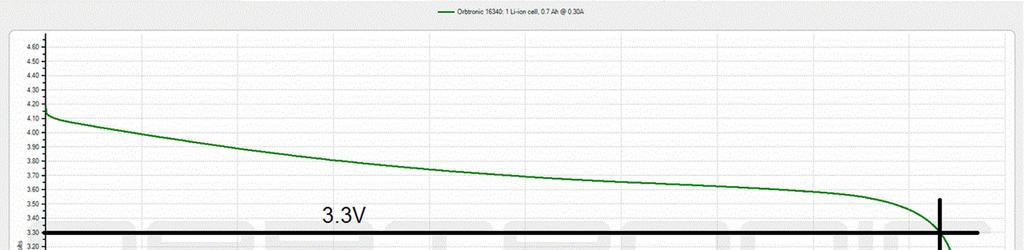
6 Battery Characteristic Source:
7 Block Diagram
8 1. System Specifications & Structure 2. Chopper Low-Noise Amplifier 3. Programmable Low-Pass Filter Channel Selector & Buffer 5. Programmable Gain Amplifier 6. Analog-Digital Converter
9 Pre-Amplifier Goals 1. Input noise cancellation a. Chopper modulation 2. Provides 40 db gain with 2 khz bandwidth 3. Adjustable cutoff frequency for different biopotentials
10 Pre-Amplifier Topology Fully differential folded cascode amplifier PMOS diff pair first stage, common source second stage Cross coupled configuration High CMRR
11 Open-loop Characteristics DC Gain Phase Margin Bandwidth 58 db 70 degrees 0-8 khz Output Voltage V
12 CMRR and PSRR 136 db from (0.5-2 khz) 90 db from (0.5-2 khz)
13 Chopper Implementation 1/f noise modulated to chopper frequency (15 khz) Subsequently eliminated by low pass filter
14 Adjustable High-pass Filter Nmos in series biased in subthreshold provides high resistance Tunable with gate voltage

15 Adjustable High-pass Filter
16 1. System Specifications & Structure 2. Chopper Low-Noise Amplifier 3. Programmable Low-Pass Filter Channel Selector & Buffer 5. Programmable Gain Amplifier 6. Analog-Digital Converter
17 OTA Used in Gm-C Filter
18 2nd-Order Programmable Gm-C Filter gm4 gm1 gm2 gm3 Gm2 used to set cutoff frequency -biasing voltage is varied
19 Adjustable Low Pass Filter Cutoff frequency can vary from 255 Hz to 2.4 khz Capacitor at 3n -a bit large
20 Full Pre-amplification Stage 40 1kHz Input
21 Pre-Amp and Gm-C Bandpass Response
22 Noise Analysis ~2.24μVrms in (0.5-2 khz)
23 Full Circuit
24 Performance Benchmarking
25 1. System Specifications & Structure 2. Chopper Low-Noise Amplifier 3. Programmable Low-Pass Filter Channel Selector & Buffer 5. Programmable Gain Amplifier 6. Analog-Digital Converter
26 Channel Selector Logic Data Select Signals Output D 2 D 1 D 0 Y S S S S S S S S7 Channel Selector
27 Channel Selector Logic Channel Selector


28 Channel Selector Logic Output Bit 0, 4, 7 Channel Selector
29 Buffer - Differential Difference Amplifier Buffer
30 DDA Open-loop Frequency Response Buffe r
31 DDA Close-loop Frequency Response Buffer
32 1. System Specifications & Structure 2. Chopper Low-Noise Amplifier 3. Programmable Low-Pass Filter Channel Selector & Buffer 5. Programmable Gain Amplifier and BGR 6. Analog-Digital Converter
33 Bandgap Reference Generator Vbiasn = 0.75 V; Vbiasp = 2.3 V PGA
34 PGA Attempted Topology PGA

35 PGA Attempted Topology Can only reach a gain of 1. Moved to other typology. PGA
36 PGA Topology Fully differential sample and hold circuit from homework assignment. Fully differential amplifier comes from Baker CH CH CF CF CH A = 1+CF/CH PGA
37 Amplification Signal, Gain = 2 PGA
38 Amplification Signal, Gain = 10 fclock = 500 K Vin f = 2K PGA
39 SW Cap Amp -- Clock Signals ph1, ph2, ph3 are non- overlapping. --A 5-transistor op-amp with a gain =1 transferring the fully differential amplifier s output signals into single ended signals to the ADC. PGA
40 1. System Specifications & Structure 2. Chopper Low-Noise Amplifier 3. Programmable Low-Pass Filter Channel Selector & Buffer 5. Programmable Gain Amplifier 6. Analog-Digital Converter
41 ADC Architecture 8-bit SAR ADC Comparator SAR Logic Binary Weighted Capacitive DAC Charge Redistribution Architecture No s/h circuit Approaches Vcm at end of cycle
42 Comparator Design Output range ICMR Power Propagation Delay Rail to Rail V < 396 uw 2.5 ns ADC
43 Comparator Layout
44 SAR Logic Schematic ADC
45 SAR Logic Layout ADC
46 DAC Schematic 1. Sampling phase 2. Hold phase 3. Charge redistribution phase ADC
47 One Throw Three Pole Switch Design ADC
48 ADC Conversion Cycle Voltage =.309 Digital Code = ADC
49 Results Dynamic Range 0 V -2.0 V Power Consumption 478 μw ADC
50 Conclusion -- Collects EEG, ECoG, EMG, ECG signal from probes; --Processes EEG, ECoG, EMG, ECG signal for μc; -- Low power consumption (~890μW, ~270μA, 3.3V) -- Portable ready
51 Future Work -- Adding control abilities on channel switching; -- Review the order of system blocks; -- Possible power optimization; -- Command library; -- Integration of the voltage regulator (risky: heat diss.)
52 Block Diagram
53 Questions?
An 8-Channel General-Purpose Analog Front-End for Biopotential Signal Measurement
 An 8-Channel General-Purpose Analog Front-End for Biopotential Signal Measurement Xue Jinming Yang, Hu, Jinming Xue Yang, Hu, Zengweijie Chen, Hang Yang Abstract This paper presents system level specifications
An 8-Channel General-Purpose Analog Front-End for Biopotential Signal Measurement
 An 8-Channel General-Purpose Analog Front-End for Biopotential Signal Measurement Xue Yang, Jinming Hu, Zengweijie Chen, Hang Yang Abstract This paper presents system level specifications of an 8 channel
A Low Power Analog Front End Capable of Monitoring Knee Movements to Detect Injury
 A Low Power Analog Front End Capable of Monitoring Knee Movements to Detect Injury Garren Boggs, Hua Chen, Sridhar Sivapurapu ECE 6414 Final Presentation Outline Motivation System Overview Analog Front
d. Can you find intrinsic gain more easily by examining the equation for current? Explain.
 EECS140 Final Spring 2017 Name SID 1. [8] In a vacuum tube, the plate (or anode) current is a function of the plate voltage (output) and the grid voltage (input). I P = k(v P + µv G ) 3/2 where µ is a
Homework 2 Summary. at the differential amplifier s inputs and sweeping V in
 Team 1 Jaehoo Choi, Xiaoshan Wang, Daniel Zhang ECE 6414 Spring 2017 Homework 2 Summary Graded HW Summary For homework 2 we graded Team 3 s submission which comprised of a fully differential amplifier
Analog CMOS Interface Circuits for UMSI Chip of Environmental Monitoring Microsystem
 Analog CMOS Interface Circuits for UMSI Chip of Environmental Monitoring Microsystem A report Submitted to Canopus Systems Inc. Zuhail Sainudeen and Navid Yazdi Arizona State University July 2001 1. Overview
LOW VOLTAGE / LOW POWER RAIL-TO-RAIL CMOS OPERATIONAL AMPLIFIER FOR PORTABLE ECG
 LOW VOLTAGE / LOW POWER RAIL-TO-RAIL CMOS OPERATIONAL AMPLIFIER FOR PORTABLE ECG A DISSERTATION SUBMITTED TO THE FACULTY OF THE GRADUATE SCHOOL OF THE UNIVERSITY OF MINNESOTA BY BORAM LEE IN PARTIAL FULFILLMENT
A Complete Analog Front-End IC Design for ECG Signal Acquisition
 A Complete Analog Front-End IC Design for ECG Signal Acquisition Yang Xu, Yanling Wu, Xiaotong Jia School of Electrical and Computer Engineering Georgia Institute of Technology yxu327@gatech.edu, yanlingwu@gatech.edu,
Design of High-Speed Op-Amps for Signal Processing
 Design of High-Speed Op-Amps for Signal Processing R. Jacob (Jake) Baker, PhD, PE Professor and Chair Boise State University 1910 University Dr. Boise, ID 83725-2075 jbaker@ieee.org Abstract - As CMOS
A Low Power Analog Front End Capable of Monitoring Knee Movements to Detect Injury
 1 A Low Power Analog Front End Capable of Monitoring Knee Movements to Detect Injury Garren Boggs, Student, IEEE, Hua Chen, Student, IEEE, Sridhar Sivapurapu, Student, IEEE Abstract This work proposes
Topology Selection: Input
 Project #2: Design of an Operational Amplifier By: Adrian Ildefonso Nedeljko Karaulac I have neither given nor received any unauthorized assistance on this project. Process: Baker s 50nm CAD Tool: Cadence
Design and Simulation of Low Voltage Operational Amplifier
 Design and Simulation of Low Voltage Operational Amplifier Zach Nelson Department of Electrical Engineering, University of Nevada, Las Vegas 4505 S Maryland Pkwy, Las Vegas, NV 89154 United States of America
IJSRD - International Journal for Scientific Research & Development Vol. 4, Issue 02, 2016 ISSN (online):
:") IJSRD - International Journal for Scientific Research & Development Vol. 4, Issue 02, 2016 ISSN (online): 2321-0613 Design & Analysis of CMOS Telescopic Operational Transconductance Amplifier (OTA) with
IJSRD - International Journal for Scientific Research & Development Vol. 4, Issue 02, 2016 ISSN (online): 2321-0613 Design & Analysis of CMOS Telescopic Operational Transconductance Amplifier (OTA) with
A 24 V Chopper Offset-Stabilized Operational Amplifier with Symmetrical RC Notch Filters having sub-10 µv offset and over-120db CMRR
 ROMANIAN JOURNAL OF INFORMATION SCIENCE AND TECHNOLOGY Volume 20, Number 4, 2017, 301 312 A 24 V Chopper Offset-Stabilized Operational Amplifier with Symmetrical RC Notch Filters having sub-10 µv offset
A DRY ELECTRODE LOW POWER CMOS EEG ACQUISITION SOC FOR SEIZURE DETECTION
 A DRY ELECTRODE LOW POWER CMOS EEG ACQUISITION SOC FOR SEIZURE DETECTION TEAM 6: MATTHIEU DURBEC, VALENTIN BERANGER, KARIM ELOUELDRHIRI ECE 6414 SPRING 2017 OUTLINE Project motivation Design overview Body-Electrode
Low Power Low Noise CMOS Chopper Amplifier
 International Journal of Electronics and Computer Science Engineering 734 Available Online at www.ijecse.org ISSN- 2277-1956 Low Power Low Noise CMOS Chopper Amplifier Parneet Kaur 1, Manjit Kaur 2, Gurmohan
ANALYSIS AND DESIGN OF HIGH CMRR INSTRUMENTATION AMPLIFIER FOR ECG SIGNAL ACQUISITION SYSTEM USING 180nm CMOS TECHNOLOGY
 International Journal of Electronics and Communication Engineering (IJECE) ISSN 2278-9901 Vol. 2, Issue 4, Sep 2013, 67-74 IASET ANALYSIS AND DESIGN OF HIGH CMRR INSTRUMENTATION AMPLIFIER FOR ECG SIGNAL
Design Analysis and Performance Comparison of Low Power High Gain 2nd Stage Differential Amplifier Along with 1st Stage
 Design Analysis and Performance Comparison of Low Power High Gain 2nd Stage Differential Amplifier Along with 1st Stage Sadeque Reza Khan Department of Electronic and Communication Engineering, National
6. OpAmp Application Examples
 Preamp MRC GmC Switched-Cap 1/31 6. OpAmp Application Examples Francesc Serra Graells francesc.serra.graells@uab.cat Departament de Microelectrònica i Sistemes Electrònics Universitat Autònoma de Barcelona
Lab 8: SWITCHED CAPACITOR CIRCUITS
 ANALOG & TELECOMMUNICATION ELECTRONICS LABORATORY EXERCISE 8 Lab 8: SWITCHED CAPACITOR CIRCUITS Goal The goals of this experiment are: - Verify the operation of basic switched capacitor cells, - Measure
Lecture 300 Low Voltage Op Amps (3/28/10) Page 300-1
 Page 300-1") Lecture 300 Low Voltage Op Amps (3/28/10) Page 300-1 LECTURE 300 LOW VOLTAGE OP AMPS LECTURE ORGANIZATION Outline Introduction Low voltage input stages Low voltage gain stages Low voltage bias circuits
Lecture 300 Low Voltage Op Amps (3/28/10) Page 300-1 LECTURE 300 LOW VOLTAGE OP AMPS LECTURE ORGANIZATION Outline Introduction Low voltage input stages Low voltage gain stages Low voltage bias circuits
NOISE IN SC CIRCUITS
 ECE37 Advanced Analog Circuits Lecture 0 NOISE IN SC CIRCUITS Richard Schreier richard.schreier@analog.com Trevor Caldwell trevor.caldwell@utoronto.ca Course Goals Deepen Understanding of CMOS analog circuit
A Novel Design of Low Voltage,Wilson Current Mirror based Wideband Operational Transconductance Amplifier
 A Novel Design of Low Voltage,Wilson Current Mirror based Wideband Operational Transconductance Amplifier Kehul A. Shah 1, N.M.Devashrayee 2 1(Associative Prof., Department of Electronics and Communication,
Pankaj Naik Electronic and Instrumentation Deptt. SGSITS, Indore, India. Priyanka Sharma Electronic and. SGSITS, Indore, India
 Designing Of Current Mode Instrumentation Amplifier For Bio-Signal Using 180nm CMOS Technology Sonu Mourya Electronic and Instrumentation Deptt. SGSITS, Indore, India Pankaj Naik Electronic and Instrumentation
CHAPTER 3 DESIGN OF PIPELINED ADC USING SCS-CDS AND OP-AMP SHARING TECHNIQUE
 CHAPTER 3 DESIGN OF PIPELINED ADC USING SCS-CDS AND OP-AMP SHARING TECHNIQUE 3.1 INTRODUCTION An ADC is a device which converts a continuous quantity into discrete digital signal. Among its types, pipelined
CMOS Instrumentation Amplifier with Offset Cancellation Circuitry for Biomedical Application
 CMOS Instrumentation Amplifier with Offset Cancellation Circuitry for Biomedical Application Author Mohd-Yasin, Faisal, Yap, M., I Reaz, M. Published 2006 Conference Title 5th WSEAS Int. Conference on
Overcoming Offset. Prof. Kofi Makinwa. Electronic Instrumentation Laboratory / DIMES Delft University of Technology Delft, The Netherlands
 Overcoming Offset Prof. Kofi Makinwa Electronic Instrumentation Laboratory / DIMES Delft University of Technology Delft, The Netherlands email: k.a.a.makinwa@tudelft.nl Motivation The offset of amplifiers
Design of a Low Power Low Noise System-on-Chip for ECG Monitoring and Diagnostic
 Design of a Low Power Low Noise System-on-Chip for ECG Monitoring and Diagnostic Yang Xu, Yanling Wu, Xiaotong Jia School of Electrical and Computer Engineering Georgia Institute of Technology yxu37@gatech.edu,
ISSN:
 468 Modeling and Design of a CMOS Low Drop-out (LDO) Voltage Regulator PRIYADARSHINI JAINAPUR 1, CHIRAG SHARMA 2 1 Department of E&CE, Nitte Meenakshi Institute of Technology, Yelahanka, Bangalore-560064,
Performance Analysis of Low Power, High Gain Operational Amplifier Using CMOS VLSI Design
 RESEARCH ARTICLE OPEN ACCESS Performance Analysis of Low Power, High Gain Operational Amplifier Using CMOS VLSI Design Ankush S. Patharkar*, Dr. Shirish M. Deshmukh** *(Department of Electronics and Telecommunication,
LINEAR IC APPLICATIONS
 1 B.Tech III Year I Semester (R09) Regular & Supplementary Examinations December/January 2013/14 1 (a) Why is R e in an emitter-coupled differential amplifier replaced by a constant current source? (b)
CHAPTER 3. Instrumentation Amplifier (IA) Background. 3.1 Introduction. 3.2 Instrumentation Amplifier Architecture and Configurations
 Background. 3.1 Introduction. 3.2 Instrumentation Amplifier Architecture and Configurations") CHAPTER 3 Instrumentation Amplifier (IA) Background 3.1 Introduction The IAs are key circuits in many sensor readout systems where, there is a need to amplify small differential signals in the presence
CHAPTER 3 Instrumentation Amplifier (IA) Background 3.1 Introduction The IAs are key circuits in many sensor readout systems where, there is a need to amplify small differential signals in the presence
DESIGN OF A PROGRAMMABLE LOW POWER LOW DROP-OUT REGULATOR
 DESIGN OF A PROGRAMMABLE LOW POWER LOW DROP-OUT REGULATOR Jayanthi Vanama and G.L.Sampoorna Trainee Engineer, Powerwave Technologies Pvt. Ltd., R&D India jayanthi.vanama@pwav.com Intern, CONEXANT Systems
Design of High Gain Low Voltage CMOS Comparator
 Design of High Gain Low Voltage CMOS Comparator Shahid Khan 1 1 Rustomjee Academy for Global Careers Abstract: Comparators used in most of the analog circuits like analog to digital converters, switching
Design of a low voltage,low drop-out (LDO) voltage cmos regulator
 voltage cmos regulator") Design of a low,low drop-out (LDO) cmos regulator Chaithra T S Ashwini Abstract- In this paper a low, low drop-out (LDO) regulator design procedure is proposed and implemented using 0.25 micron CMOS process.
Design of a low,low drop-out (LDO) cmos regulator Chaithra T S Ashwini Abstract- In this paper a low, low drop-out (LDO) regulator design procedure is proposed and implemented using 0.25 micron CMOS process.
A Compact Folded-cascode Operational Amplifier with Class-AB Output Stage
 A Compact Folded-cascode Operational Amplifier with Class-AB Output Stage EEE 523 Advanced Analog Integrated Circuits Project Report Fuding Ge You are an engineer who is assigned the project to design
DESIGNING OF CURRENT MODE INSTRUMENTATION AMPLIFIER FOR BIO-SIGNAL USING 180NM CMOS TECHNOLOGY
 DESIGNING OF CURRENT MODE INSTRUMENTATION AMPLIFIER FOR BIO-SIGNAL USING 180NM CMOS TECHNOLOGY GAYTRI GUPTA AMITY University Email: Gaytri.er@gmail.com Abstract In this paper we have describes the design
Radivoje Đurić, 2015, Analogna Integrisana Kola 1
 Low power OTA 1 Two-Stage, Miller Op Amp Operating in Weak Inversion Low frequency response: gm1 gm6 Av 0 g g g g A v 0 ds2 ds4 ds6 ds7 I D m, ds D nvt g g I n GB and SR: GB 1 1 n 1 2 4 6 6 7 g 2 2 m1
A Low Power Gain Boosted Fully Differential OTA for a 10bit pipelined ADC
 IOSR Journal of Engineering e-issn: 2250-3021, p-issn: 2278-8719, Vol. 2, Issue 12 (Dec. 2012) V2 PP 22-27 A Low Power Gain Boosted Fully Differential OTA for a 10bit pipelined ADC A J Sowjanya.K 1, D.S.Shylu
10-Bit 5MHz Pipeline A/D Converter. Kannan Sockalingam and Rick Thibodeau
 10-Bit 5MHz Pipeline A/D Converter Kannan Sockalingam and Rick Thibodeau July 30, 2002 Contents 1 Introduction 8 1.1 Project Overview........................... 8 1.2 Objective...............................
Design for MOSIS Education Program
 Design for MOSIS Education Program (Research) T46C-AE Project Title Low Voltage Analog Building Block Prepared by: C. Durisety, S. Chen, B. Blalock, S. Islam Institution: Department of Electrical and Computer
Design of Miller Compensated Two-Stage Operational Amplifier for Data Converter Applications
 Design of Miller Compensated Two-Stage Operational Amplifier for Data Converter Applications Prema Kumar. G Shravan Kudikala Casest, School Of Physics Casest, School Of Physics University Of Hyderabad
ECE 415/515 ANALOG INTEGRATED CIRCUIT DESIGN
 ECE 415/515 ANALOG INTEGRATED CIRCUIT DESIGN OPAMP DESIGN AND SIMULATION Vishal Saxena OPAMP DESIGN PROJECT R 2 v out v in /2 R 1 C L v in v out V CM R L V CM C L V CM -v in /2 R 1 C L (a) (b) R 2 ECE415/EO
A 16Ω Audio Amplifier with 93.8 mw Peak loadpower and 1.43 quiscent power consumption
 A 16Ω Audio Amplifier with 93.8 mw Peak loadpower and 1.43 quiscent power consumption IEEE Transactions on circuits and systems- Vol 59 No:3 March 2012 Abstract A class AB audio amplifier is used to drive
Design of Low Power Preamplifier Latch Based Comparator
 Design of Low Power Preamplifier Latch Based Comparator Siddharth Bhat SRM University India siddharth.bhat05@gmail.com Shubham Choudhary SRM University India shubham.choudhary8065@gmail.com Jayakumar Selvakumar
c 2013 MD. NAIMUL HASAN ALL RIGHTS RESERVED
 c 2013 MD. NAIMUL HASAN ALL RIGHTS RESERVED A COMPACT LOW POWER BIO-SIGNAL AMPLIFIER WITH EXTENDED LINEAR OPERATION RANGE A Thesis Presented to The Graduate Faculty of The University of Akron In Partial
Analog Integrated Circuit Design Exercise 1
 Analog Integrated Circuit Design Exercise 1 Integrated Electronic Systems Lab Prof. Dr.-Ing. Klaus Hofmann M.Sc. Katrin Hirmer, M.Sc. Sreekesh Lakshminarayanan Status: 21.10.2015 Pre-Assignments The lecture
TWO AND ONE STAGES OTA
 TWO AND ONE STAGES OTA F. Maloberti Department of Electronics Integrated Microsystem Group University of Pavia, 7100 Pavia, Italy franco@ele.unipv.it tel. +39-38-50505; fax. +39-038-505677 474 EE Department
Op-Amp Design Project EE 5333 Analog Integrated Circuits Prof. Ramesh Harjani Department of ECE University of Minnesota, Twin Cities Report prepared
 Op-Amp Design Project EE 5333 Analog Integrated Circuits Prof. Ramesh Harjani Department of ECE University of Minnesota, Twin Cities Report prepared by: Nirav Desai (4280229) 1 Contents: 1. Design Specifications
Design of a Folded Cascode Operational Amplifier in a 1.2 Micron Silicon-Carbide CMOS Process
 University of Arkansas, Fayetteville ScholarWorks@UARK Electrical Engineering Undergraduate Honors Theses Electrical Engineering 5-2017 Design of a Folded Cascode Operational Amplifier in a 1.2 Micron
Performance Evaluation of Different Types of CMOS Operational Transconductance Amplifier
 Performance Evaluation of Different Types of CMOS Operational Transconductance Amplifier Kalpesh B. Pandya 1, Kehul A. shah 2 1 Gujarat Technological University, Department of Electronics & Communication,
ELM824xA 3.0μA Very low power CMOS dual operational amplifier
 ELM824xA 3.μA Very low power CMOS dual operational amplifier General description ELM824xA is a very low current consumption-typ.3.μa CMOS dual OP-AMP provided with a wide common mode input voltage range.
A Design of Sigma-Delta ADC Using OTA
 RESEARCH ARTICLE OPEN ACCESS A Design of Sigma-Delta ADC Using OTA Miss. Niveditha Yadav M 1, Mr. Yaseen Basha 2, Dr. Venkatesh kumar H 3 1 Department of ECE, PG Student, NCET/VTU, and Bengaluru, India
Design and Implementation of High Gain, High Bandwidth CMOS Folded cascode Operational Transconductance Amplifier
 Design and Implementation of High Gain, High Bandwidth CMOS Folded cascode Operational Transconductance Amplifier Jalpa solanki, P.G Student, Electronics and communication, SPCE Visnagar, India jalpa5737@gmail.com
EEC 210 Fall 2008 Design Project. Rajeevan Amirtharajah Dept. of Electrical and Computer Engineering University of California, Davis
 EEC 210 Fall 2008 Design Project Rajeevan Amirtharajah Dept. of Electrical and Computer Engineering University of California, Davis Issued: November 18, 2008 Due: December 5, 2008, 5:00 PM in my office.
A Low Power Low-Noise Low-Pass Filter for Portable ECG Detection System
 I J C T A, 9(41), 2016, pp. 95-103 International Science Press ISSN: 0974-5572 A Low Power Low-Noise Low-Pass Filter for Portable ECG Detection System Rajeev Kumar*, Sanjeev Sharma** and Rishab Goyal***
Design and implementation of two stage operational amplifier
 Design and implementation of two stage operational amplifier Priyanka T 1, Dr. H S Aravind 2, Yatheesh Hg 3 1M.Tech student, Dept, of ECE JSSATE Bengaluru 2Professor and HOD, Dept, of ECE JSSATE Bengaluru
Nizamuddin M., International Journal of Advance Research, Ideas and Innovations in Technology.
 ISSN: 2454-132X Impact factor: 4.295 (Volume3, Issue1) Available online at: www.ijariit.com Design & Performance Analysis of Instrumentation Amplifier at Nanoscale Dr. M. Nizamuddin Assistant professor,
Radivoje Đurić, 2015, Analogna Integrisana Kola 1
 OTA-output buffer 1 According to the types of loads, the driving capability of the output stages differs. For switched capacitor circuits which have high impedance capacitive loads, class A output stage
ACUTE Respiratory Distress Syndrome (ARDS) is a condition
 is a condition") An Electrical Impedance Tomography Analog Front End for Lung Ventilation Monitoring Jaehoo Choi, Xiaoshan Wang and Daniel Zhang Electrical and Computer Engineering Georgia Institute of Technology GA, USA
An Electrical Impedance Tomography Analog Front End for Lung Ventilation Monitoring Jaehoo Choi, Xiaoshan Wang and Daniel Zhang Electrical and Computer Engineering Georgia Institute of Technology GA, USA
NOVEMBER 29, 2017 COURSE PROJECT: CMOS TRANSIMPEDANCE AMPLIFIER ECG 720 ADVANCED ANALOG IC DESIGN ERIC MONAHAN
 NOVEMBER 29, 2017 COURSE PROJECT: CMOS TRANSIMPEDANCE AMPLIFIER ECG 720 ADVANCED ANALOG IC DESIGN ERIC MONAHAN 1.Introduction: CMOS Transimpedance Amplifier Avalanche photodiodes (APDs) are highly sensitive,
Operational Amplifier with Two-Stage Gain-Boost
 Proceedings of the 6th WSEAS International Conference on Simulation, Modelling and Optimization, Lisbon, Portugal, September 22-24, 2006 482 Operational Amplifier with Two-Stage Gain-Boost FRANZ SCHLÖGL
EE 330 Lecture 34. Guest Lecture. Why are there so many Op Amps?
 EE 330 Lecture 34 Guest Lecture Why are there so many Op Amps? by Jerry Doorenbos of Texas Instruments 1 Op Amp Technology Overview Developed by Art Kay, Thomas Kuehl, and Tim Green Precision Amplifiers
A PSEUDO-CLASS-AB TELESCOPIC-CASCODE OPERATIONAL AMPLIFIER
 A PSEUDO-CLASS-AB TELESCOPIC-CASCODE OPERATIONAL AMPLIFIER M. Taherzadeh-Sani, R. Lotfi, and O. Shoaei ABSTRACT A novel class-ab architecture for single-stage operational amplifiers is presented. The structure
Design of Rail-to-Rail Op-Amp in 90nm Technology
 IJSTE - International Journal of Science Technology & Engineering Volume 1 Issue 2 August 2014 ISSN(online) : 2349-784X Design of Rail-to-Rail Op-Amp in 90nm Technology P R Pournima M.Tech Electronics
DESIGN OF RAIL-TO-RAIL OPERATIONAL AMPLIFIER USING XFAB 0.35µM PROCESS
 DESIGN OF RAIL-TO-RAIL OPERATIONAL AMPLIFIER USING XFAB 0.35µM PROCESS A DISSERTATION SUBMITTED TO THE FACULTY OF UNIVERSITY OF MINNESOTA BY NAMRATA ANAND DATE IN PARTIAL FULFILLMENT OF THE REQUIREMENTS
Design of Operational Amplifier in 45nm Technology
 Design of Operational Amplifier in 45nm Technology Aman Kaushik ME Scholar Dept. of E&CE, NITTTR Chandigarh Abstract-This paper presents the designing and performance analysis of Operational Transconductance
Low Quiescent Power CMOS Op-Amp in 0.5µm Technology
 Kevin Fronczak - Low Power CMOS Op-Amp - Rochester Institute of Technology EE610 1 Low Quiescent Power CMOS Op-Amp in 0.5µm Technology Kevin C. Fronczak Abstract This paper analyzes a low quiescent power
A CMOS Low-Voltage, High-Gain Op-Amp
 A CMOS Low-Voltage, High-Gain Op-Amp G N Lu and G Sou LEAM, Université Pierre et Marie Curie Case 203, 4 place Jussieu, 75252 Paris Cedex 05, France Telephone: (33 1) 44 27 75 11 Fax: (33 1) 44 27 48 37
Design of Gain Enhanced and Power Efficient Op- Amp for ADC/DAC and Medical Applications
 Indian Journal of Science and Technology, Vol 9(29), DOI: 10.17485/ijst/2016/v9i29/90885, August 2016 ISSN (Print) : 0974-6846 ISSN (Online) : 0974-5645 Design of Gain Enhanced and Power Efficient Op-
DESIGN OF LOW POWER SAR ADC FOR ECG USING 45nm CMOS TECHNOLOGY
 DESIGN OF LOW POWER SAR ADC FOR ECG USING 45nm CMOS TECHNOLOGY Silpa Kesav 1, K.S.Nayanathara 2 and B.K. Madhavi 3 1,2 (ECE, CVR College of Engineering, Hyderabad, India) 3 (ECE, Sridevi Women s Engineering
This document is downloaded from DR-NTU, Nanyang Technological University Library, Singapore.
 This document is downloaded from DR-NTU, Nanyang Technological University Library, Singapore. Title An ultra low-power CMOS EMG amplifier with high efficiency in operation frequency per power Author(s
Problem three helps in changing the biasing of the circuit to operate at a lower VDD but it comes at a cost of increased power.
 Summary By Saad Bin Nasir HW#3 helps us learn the following key components Problem one helps us understand the distribution of vds on the output transistors of an amplifier. Improved biasing can be made
EC kHz, 7μA, CMOS, Rail-to-Rail Operational Amplifier. General Description. Features. Applications. Pin Assignments
 General Description Features The is a single supply, low power CMOS operational amplifier; these amplifiers offer bandwidth of 250kHz, rail-to-rail inputs and outputs, and single-supply operation from
Fully differential RF ADC Driver XT06
 Fully differential RF ADC Driver XT06 DATA SHEET FEATURES FUNCTIONAL BLOCK DIAGRAM 3 db bandwidth of up to 350 MHz Adjustable output common-mode voltage Externally adjustable gain Slew rate 880 V/us at
Design of High Gain Two stage Op-Amp using 90nm Technology
 Design of High Gain Two stage Op-Amp using 90nm Technology Shaik Aqeel 1, P. Krishna Deva 2, C. Mahesh Babu 3 and R.Ganesh 4 1 CVR College of Engineering/UG Student, Hyderabad, India 2 CVR College of Engineering/UG
Design and Simulation of Low Dropout Regulator
 Design and Simulation of Low Dropout Regulator Chaitra S Kumar 1, K Sujatha 2 1 MTech Student, Department of Electronics, BMSCE, Bangalore, India 2 Assistant Professor, Department of Electronics, BMSCE,
Ultra Low Power Multistandard G m -C Filter for Biomedical Applications
 Volume-7, Issue-5, September-October 2017 International Journal of Engineering and Management Research Page Number: 105-109 Ultra Low Power Multistandard G m -C Filter for Biomedical Applications Rangisetti
A Successive Approximation ADC based on a new Segmented DAC
 A Successive Approximation ADC based on a new Segmented DAC segmented current-mode DAC successive approximation ADC bi-direction segmented current-mode DAC DAC INL 0.47 LSB DNL 0.154 LSB DAC 3V 8 2MS/s
Ultra Low Static Power OTA with Slew Rate Enhancement
 ECE 595B Analog IC Design Design Project Fall 2009 Project Proposal Ultra Low Static Power OTA with Slew Rate Enhancement Patrick Wesskamp PUID: 00230-83995 1) Introduction In this design project I plan
AD8232 EVALUATION BOARD DOCUMENTATION
 One Technology Way P.O. Box 9106 Norwood, MA 02062-9106 Tel: 781.329.4700 Fax: 781.461.3113 www.analog.com AD8232 EVALUATION BOARD DOCUMENTATION FEATURES Ready to use Heart Rate Monitor (HRM) Front end
HT9291/HT9292/HT9294 TinyPower TM Operation Amplifier
 TinyPower TM Operation Amplifier Features Wide operating voltage: 1.4V to 5.5V Low quiescent current: typical 0.6µA/amplifier Rail-to-Rail output Gain bandwidth: 11kHz typical Unity gain stable Available
Low-Voltage Wide Linear Range Tunable Operational Transconductance Amplifier
 Low-Voltage Wide Linear Range Tunable Operational Transconductance Amplifier A dissertation submitted in partial fulfillment of the requirement for the award of degree of Master of Technology in VLSI Design
EECS 140/240A Final Project spec, version 1 Spring 17. FINAL DESIGN due Monday, 5/1/2017 9am
 EECS 140/240A Final Project spec, version 1 Spring 17 FINAL DESIGN due Monday, 5/1/2017 9am 1 1.2 no layout? XC? Golden Bear Circuits is working on its next exciting circuit product. This is a mixedsignal
What? nanowatt? Acquiring sensor data in wireless products with nanowatts of power consumption
 11001101011010 10101010101010 10101010111010 01010011101101 010101 What? nanowatt? Acquiring sensor data in wireless products with nanowatts of power consumption Peggy Liska Texas Instruments Product Marketing
A 25MS/s 14b 200mW Σ Modulator in 0.18µm CMOS
 UT Mixed-Signal/RF Integrated Circuits Seminar Series A 25MS/s 14b 200mW Σ Modulator in 0.18µm CMOS Pio Balmelli April 19 th, Austin TX 2 Outline VDSL specifications Σ A/D converter features Broadband
What is the typical voltage gain of the basic two stage CMOS opamp we studied? (i) 20dB (ii) 40dB (iii) 80dB (iv) 100dB
 20dB (ii) 40dB (iii) 80dB (iv) 100dB") Department of Electronic ELEC 5808 (ELG 6388) Signal Processing Electronics Final Examination Dec 14th, 2010 5:30PM - 7:30PM R. Mason answer all questions one 8.5 x 11 crib sheets allowed 1. (5 points)
Department of Electronic ELEC 5808 (ELG 6388) Signal Processing Electronics Final Examination Dec 14th, 2010 5:30PM - 7:30PM R. Mason answer all questions one 8.5 x 11 crib sheets allowed 1. (5 points)
Low Power and Fast Transient High Swing CMOS Telescopic Operational Amplifier
 RESEARCH ARTICLE OPEN ACCESS Low Power and Fast Transient High Swing CMOS Telescopic Operational Amplifier Akshay Kumar Kansal 1, Asst Prof. Gayatri Sakya 2 Electronics and Communication Department, 1,2
Homework Assignment 10
 Homework Assignment 10 Question The amplifier below has infinite input resistance, zero output resistance and an openloop gain. If, find the value of the feedback factor as well as so that the closed-loop
EMG Sensor Shirt. Senior Project Written Hardware Description April 28, 2015 ETEC 474. By: Dylan Kleist Joshua Goertz
 EMG Sensor Shirt Senior Project Written Hardware Description April 28, 2015 ETEC 474 By: Dylan Kleist Joshua Goertz Table of Contents Introduction... 3 User Interface Board... 3 Bluetooth... 3 Keypad...
High Voltage Operational Amplifiers in SOI Technology
 High Voltage Operational Amplifiers in SOI Technology Kishore Penmetsa, Kenneth V. Noren, Herbert L. Hess and Kevin M. Buck Department of Electrical Engineering, University of Idaho Abstract This paper
@IJMTER-2016, All rights Reserved 333
 Design of High Performance CMOS Comparator using 90nm Technology Shankar 1, Vasudeva G 2, Girish J R 3 1 Alpha college of Engineering, 2 Knowx Innovations, 3 sjbit Abstract- In many digital circuits the
Advanced Operational Amplifiers
 IsLab Analog Integrated Circuit Design OPA2-47 Advanced Operational Amplifiers כ Kyungpook National University IsLab Analog Integrated Circuit Design OPA2-1 Advanced Current Mirrors and Opamps Two-stage
Index terms: Analog to Digital conversion, capacitor sharing, high speed OPAMP-sharing pipelined analog to digital convertor, Low power.
 Pipeline ADC using Switched Capacitor Sharing Technique with 2.5 V, 10-bit Ankit Jain Dept. of Electronics and Communication, Indore Institute of Science & Technology, Indore, India Abstract: This paper
Chapter 13 Oscillators and Data Converters
 Chapter 13 Oscillators and Data Converters 13.1 General Considerations 13.2 Ring Oscillators 13.3 LC Oscillators 13.4 Phase Shift Oscillator 13.5 Wien-Bridge Oscillator 13.6 Crystal Oscillators 13.7 Chapter
16 V, 1 MHz, CMOS Rail-to-Rail Input/Output Operational Amplifier ADA4665-2
 6 V, MHz, CMOS Rail-to-Rail Input/Output Operational Amplifier ADA4665-2 FEATURES Lower power at high voltage: 29 μa per amplifier typical Low input bias current: pa maximum Wide bandwidth:.2 MHz typical
An Analog Phase-Locked Loop
 1 An Analog Phase-Locked Loop Greg Flewelling ABSTRACT This report discusses the design, simulation, and layout of an Analog Phase-Locked Loop (APLL). The circuit consists of five major parts: A differential
Amplifiers Frequency Response Examples
 ECE 5/45 Analog IC Design We will use the following MOSFET parameters for hand-calculations and the µm CMOS models for corresponding simulations. Table : Long-channel MOSFET parameters. Parameter NMOS
1.8 V Low Power CMOS Rail-to-Rail Input/Output Operational Amplifier AD8515
 Data Sheet FEATURES Single-supply operation: 1.8 V to 5 V Offset voltage: 6 mv maximum Space-saving SOT-23 and SC7 packages Slew rate: 2.7 V/μs Bandwidth: 5 MHz Rail-to-rail input and output swing Low
Design of an Amplifier for Sensor Interfaces
 Design of an Amplifier for Sensor Interfaces Anurag Mangla Electrical and Electronics Engineering anurag.mangla@epfl.ch Supervised by Dr. Marc Pastre Prof. Maher Kayal Outline Introduction Need for high