1. General Description
|
|
|
- Silvester Goodwin
- 5 years ago
- Views:
Transcription
1 AK9721AE LED Driver and Sensor AFE for NDIR Gas Sensing 1. General Description The AK9721AE is the IR LED driver and Analog Front End (AFE) IC for signal processing of IR photo detector. The AK9721AE has dual channel AFE and an ADC for digital output, and IR photo detector output signals can be obtained at the same time. The AK9721AE can communicate with HOST MCU through I 2 C bus. The AK9721AE is suitable for NDIR gas sensing processing using IR LED and IR photo detector. 2. Features Integrated LED Driver with Programmable Constant Current Circuit Dual Channel Input AFE Interrupt Function Power Supply Voltage Range: 2.7V to 3.6V Low Current Consumption: Typ. 8.1μA (Integration time:100μs, Measurement time: 149ms) Small and Thin Package: 16-pin QFN 3.0mm x 3.0mm x t0.7mm CO 2 Sensor for HVAC System CO 2 refrigerant leakage detection 3. Applications - 1 -
2 4. Table of Contents 1. General Description Features Applications Table of Contents Block Diagram and Functions Block Diagram Functions Pin Configurations and Functions Pin Configurations Functions Absolute Maximum Ratings Recommended Operating Conditions Power Supply Conditions Electrical Characteristics Analog Characteristics Connection device specification Digital Characteristics DC Characteristics AC Characteristics Functional Descriptions Power Supply States Reset Functions Operating Mode Descriptions for Each Operating Mode Power Down Mode (PDN pin = L ) Stand-by Mode (MODE[1:0] bits = 00 ) Single Measurement Mode (MODE[1:0] bits = 10 ) Sensor Resistance Measurement Mode (MODE[1:0] bits = 10 and RES_MEAS bit = 1 ) Read Measurement Data Readout Procedure Example of Read-out Procedure Serial Interface Data Transfer Changing state of the SDA line Start / Stop Conditions Acknowledge Slave Address WRITE Command READ Command Registers Description of Registers Register Map Detailed Description of Register WIA1: Company code WIA2: Device ID INFO1, INFO2: Information ST1: Status IRxL, IRxM, IRxH: Measurement data of IR sensor(x=1,2) TMPL, TMPH: Measurement data of temperature sensor Vf: Measurement data of LED forward voltage CNTL1: Control
3 CNTL2: Control CNTL3: Control CNTL4: Control CNTL5: Control CNTL6: Control CNTL7: Control CNTL8: Control CNTL9: Control CNTL10: Control Example of Recommended External Circuits Package Outline Dimensions Pad Dimensions Marking Ordering Guide Revision History IMPORTANT NOTICE

 to voltage. Cancel the offset of IR photo detector.")
4 5. Block Diagram and Functions 5.1. Block Diagram Figure 4.1 Block Diagram 5.2. Functions Block OSC VIREF TSENS AFE1 AFE2 ADC1 / 2 LED DRIVER REGU I 2 C I/F SEQUENCER REGISTER ADVREF GEN1 / 2 SH PRE SH Table 4.1 Block Functions Function Oscillator Reference voltage and reference current generator Temperature sensor Convert the IR photo detector output current path1 (IR1 path) to voltage. Cancel the offset of IR photo detector. Convert the IR photo detector output current path2 (IR2 path) to voltage. Cancel the offset of IR photo detector. Sigma delta 2nd order analog-to-digital converter LED constant current driver Generate 1.6V for digital circuit Communicate with MCU by SCL and SDA in I 2 C protocol. Support 400kHz fast mode. Control of analog circuit Register to store the measurement data, operation mode, timing value Reference voltage generator for ADC Sample and hold circuit Sample and hold circuit - 4 -
. SCL is connected to AVDD voltage through a pull-up resistor. 2 SDA I/O I2 C data input/output pin. This pin is open drain pin output(nmos type).")
5 6. Pin Configurations and Functions 6.1. Pin Configurations Figure 5.1 Pin Configurations 6.2. Functions Table 5.1 Pin Functions Pin No. Name I/O Functions 1 SCL I I 2 C clock input pin. This pin is open drain pin output(nmos type). SCL is connected to AVDD voltage through a pull-up resistor. 2 SDA I/O I2 C data input/output pin. This pin is open drain pin output(nmos type). SDA is connected to AVDD voltage through a pull-up resistor. Interrupt pin. INTN pin is active low at the ADC output is ready for 3 INTN O read. This pin is open drain output(nmos type). INTN is connected to AVDD voltage through a pull-up resister. 4 PDN I Power down pin. When PDN pin = H, The AK9721AE can operate. 5 TEST1 I TEST pin. TEST pin should be connected to VSS 6 TEST2 I TEST pin. TEST pin should be connected to VSS 7 TEST3 I TEST pin. TEST pin should be connected to VSS 8 TEST4 I TEST pin. TEST pin should be connected to VSS 9 SINA1 I IR photo ditector1 connection pin (anode) 10 SINC1 I IR photo ditector1 connection pin (cathode) 11 SINC2 I IR photo ditector2 connection pin (cathode) 12 SINA2 I IR photo ditector2 connection pin (anode) 13 LEDO O LED driver output pin 14 FVDD - LED driver power supply pin 15 VSS - Ground pin 16 AVDD - Power supply pin - 5 -

6 7. Absolute Maximum Ratings Table 7.1 Absolute Maximum Ratings (VSS = 0V) Parameter Symbol Min. Max. Unit Power supply AVDD, FVDD pins V V Input voltage All pins Vin V Input current All pins(except for power supply) Iin ma Storage temperature Tstg C WARNING: Operation at or beyond these limits may result in permanent damage to the device. Normal operation is not guaranteed at these extremes. 8. Recommended Operating Conditions Table 8.1 Recommended Operating Conditions (VSS = 0V) Parameter Symbol Min. Typ. Max. Unit Power supply AVDD, FVDD pins V V Operation temperature Ta C 9. Power Supply Conditions Table 9.1 Power Supply Conditions (Unless otherwise specified, AVDD = 2.7 ~ 3.6V, Ta = -40 ~ 90ºC) Parameter Symbol Min. Typ. Max. Unit Power supply PDN pin PSUP 200 μs Figure 9.1 Power supply conditions - 6 -
7 10. Electrical Characteristics Analog Characteristics Table 10.1 Electrical Characteristics (Unless otherwise specified, AVDD = 2.7 ~ 3.6V, Ta = -40 ~ 90ºC) Parameter Symbol Min. Typ. Max. Unit IR sensor input current range 1 IR sensor input current range 2 IR sensor output noise 1 IR sensor output noise 2 Sensor resistance measurement range 1 Sensor resistance measurement range 2 LED forward voltage measurement range LED current accuracy LED current step Current consumption IR1 path IR1_AFE_GAIN[1:0] bits = 01 ITIME[7:0] bits = IR2 path ITIME[7:0] bits = IR1 path MLOOP[7:0] bits= IR1_AFE_GAIN[1:0] bits = 00 ITIME[7:0] bits = R01 = 33kΩ Ta = 25 ºC IR2 path ITIME[7:0] bits = R02 = 33kΩ Ta = 25 ºC IR1 path Sensor resistance measurement mode IR2 path Sensor resistance measurement mode LEDDADJ[4:0] bits= LEDO pin = 1.5V Ta = 25 ºC LEDO pin = 1.5V AVDD pin = 2.7V Ta = 25 ºC Stand-by mode MODE[1:0] bits = 00 Single measurement mode MODE[1:0] bits = 10 MTIME[7:0] bits = ITIME[7:0] bits = LEDADJ[4:0] bits = Single measurement mode MODE[1:0] bits = 10 MTIME[7:0] bits = ITIME[7:0] bits = LEDADJ[4:0] bits = Single measurement mode MODE[1:0] bits = 10 MTIME[7:0] bits = ITIME[7:0] bits = LEDADJ[4:0] bits = Note: * 1. Reference data only, not tested * 2. Total average current of AK9721AE and LED * 3. Total peak current of AK9721AE and LED SIR na SIR μa SON LSBrms SON LSBrms kω kω VFMR V ma ma IDD μa IDD μa IDD2 (* 1,2) IDD3 (* 1) IDD4 (* 1,2) IDD5 (* 1,2,3) 8.9 ma 8.1 μa 160 μa 102 ma IDD6(* 1) 5.4 μa - 7 -
8 Connection device specification Table 10.2 Connection device specification (Unless otherwise specified, AVDD = 2.7 ~ 3.6V, Ta = -40 ~ 90ºC) Parameter Symbol Min. Typ. Max. Unit Input current 1 IR1 path ISIN na Input current 2 IR2 path ISIN μa IR sensor resistance 1 IR1 path Ta = 25 ºC R kω IR sensor resistance 2 IR2 path Ta = 25 ºC R kω Digital Characteristics DC Characteristics Table 10.3 DC Characteristics (Unless otherwise specified, AVDD = 2.7 ~ 3.6V, Ta = -40 ~ 90ºC) Parameter Symbol Min. Typ. Max. Unit SCL, High level input voltage1 SDA pins VIH1 70%AVDD AVDD+0.3 V PDN pin VIH2 80%AVDD AVDD+0.3 Low level input voltage PDN, SCL, VIL 30%AVDD V Input current Vin = VSS or AVDD Hysteresis voltage (*3) Low level IOL 3mA output voltage Note: * 3. Reference data only, not tested SDA pins PDN, SCL, SDA pins SCL, SDA pins SDA, INTN pins Iin μa VHS 5%AVDD V VOL 20%AVDD V - 8 -
9 AC Characteristics Table 10.4 AC Characteristics (Standard Mode: fscl 100kHz) (Unless otherwise specified, AVDD = 2.7 ~ 3.6V, Ta = -40 ~ 90ºC) Parameter Symbol Min. Typ. Max. Unit SCL clock frequency fscl 100 khz SCL clock high period thigh 4.0 µs SCL clock low period tlow 4.7 µs SDA and SCL rise time (*4) tr 1.0 µs SDA and SCL fall time (*4) tf 0.3 µs Start condition hold time thd:sta 4.0 µs Start condition setup time tsu:sta 4.7 µs SDA hold time (vs. SCL falling edge) thd:dat 0 µs SDA setup time (vs. SCL rising edge) tsu:dat 250 ns Stop condition setup time tsu:sto 4.0 µs Bus free time fbuf 4.7 µs Note: *4. Reference data only, not tested Table 10.5 AC Characteristics (Fast Mode: 100kHz fscl 400kHz) (Unless otherwise specified, AVDD = 2.7 ~ 3.6V, Ta = -40 ~ 90ºC) Parameter Symbol Min. Typ. Max. Unit SCL clock frequency fscl 400 khz SCL clock high period thigh 0.6 µs SCL clock low period tlow 1.3 µs SDA and SCL rise time (*5) tr 0.3 µs SDA and SCL fall time (*5) tf 0.3 µs Start condition hold time thd:sta 0.6 µs Start condition setup time tsu:sta 0.6 µs SDA hold time (vs. SCL falling edge) thd:dat 0 µs SDA setup time (vs. SCL rising edge) tsu:dat 100 ns Stop condition setup time tsu:sto 0.6 µs Bus free time fbuf 1.3 µs Noise suppression pulse width tsp 50 ns Note: *5. Reference data only, not tested
![[I 2 C bus interface timing] SDA tbuf tlow tr thigh tf tsp VIH VIL SCL VIH VIL thd:sta thd:dat tsu:dat tsu:sta](/docs-images/81/84621017/images/10-0.jpg "tsu:sto Stop Start Start Stop Figure 10.1 Bus Timing Table 10.")
 Parameter Symbol Min. Typ. Max. Unit Rise time(*6) INTN pin trintn 2.")

10 [I 2 C bus interface timing] SDA tbuf tlow tr thigh tf tsp VIH VIL SCL VIH VIL thd:sta thd:dat tsu:dat tsu:sta tsu:sto Stop Start Start Stop Figure 10.1 Bus Timing Table 10.6 AC Characteristics of the INTN pin (Unless otherwise specified, AVDD = 2.7 ~ 3.6V, Ta = -40 ~ 90ºC) Parameter Symbol Min. Typ. Max. Unit Rise time(*6) INTN pin trintn 2.0 µs Fall time(*6) RL = 24kΩ CL = 50pF tfintn 0.25 µs Note: *6. Reference data only, not tested Figure 10.2 INTN load circuit Table 10.7 AC Characteristics of the PDN pin (Unless otherwise specified, AVDD = 2.7 ~ 3.6V, Ta = -40 ~ 90ºC) Parameter Symbol Min. Typ. Max. Unit PDN pulse width PDN pin tpdn 1 µs Figure 10.3 PDN condition
11 11.1. Power Supply States 11. Functional Descriptions Table 11.1 Power Supply States and Functions State AVDD pin, FVDD pin PDN pin I 2 C Analog Circuit IDD 1 OFF(0V) L Disable Power Down Unknown ~ 3.6V L Disable Only the regulator circuit < 3.0µA operates ~ 3.6V H Enable Only the regulator circuit operates < 3.0µA Reset Functions The AK9721AE has three reset functions. (1) Hardware reset The AK9721AE is reset by PDN pin = L (2) Soft reset The AK9721AE is reset by setting SRST bit. When the AK9721AE is reset, all registers are set to initial values Operating Mode The AK9721AE has following four operation modes. (1) Power Down Mode (2) Stand-by Mode (3) Single Measurement Mode (4) Sensor Resistance Measurement Mode
12 Power Down Mode: The all circuits are powered down for saving the current consumption. PDN= H PDN= L Stand-by Mode MODE [1:0] bits = 10 MODE [1:0] bits = 00, 01, 11 Automatic shift Single measurement mode: The measurement is done, and saving the data on the register. Stand-by mode is automatically after measurement ended. RES_MEAS bit = 1 MODE [1:0] bits = 10 MODE [1:0] bits = 00, 01, 11 Automatic shift Sensor resistance measurement mode: The measurement is done, and saving the data on the register. Stand-by mode is automatically after measurement ended. Figure 11.1 Operating Mode Descriptions for Each Operating Mode Power Down Mode (PDN pin = L ) All circuits are powered off with PDN pin = L. The all functions of the AK9721AE do not work in this mode Stand-by Mode (MODE[1:0] bits = 00 ) Power to the circuits except for the regulator is off. All registers can be access in this mode. Read / Write register data are retained, and reset by software reset Single Measurement Mode (MODE[1:0] bits = 10 ) When the AK9721AE is set to single measurement mode (MODE [1:0] bits = 10 ), measurement is done once, and the measurement data is stored to the measurement data registers (IR1L to VFH). After completing measurement, The AK9721AE output Low from INTN pin and goes to stand-by mode (MODE [1:0] bits = 00 ) automatically
13 MODE[1:0] "00" Change the register Read data Change the register "10" (Single measurement mode) "00" (Stand-by Mode) "10" MLOOP[7:0] setting Intermediate data Measure 1 Measure 2 Measure M Measure 1 Measurement data Data(N) Data(N) Interrupt Data is ready Analog MTIME[7:0] setting OFF ON OFF ON LED driver ON IR sensor measurement LED off time = (Integration time x ) x 8 μs IR sensor measurement LED on time = Integration time x μs Temperature measurement Vf measurement Figure 11.2 Single Measurement Mode Sensor Resistance Measurement Mode (MODE[1:0] bits = 10 and RES_MEAS bit = 1 ) After setting the sensor resistance measurement mode (RES_MEAS bit = 1 ), execute the single measurement mode, you can measure the resistance value of the IR sensor. Measurement results are stored in the IR measurement data registers. After completing measurement, The AK9721AE output Low from INTN pin and goes to stand-by mode (MODE [1:0] bits = 00 ) automatically
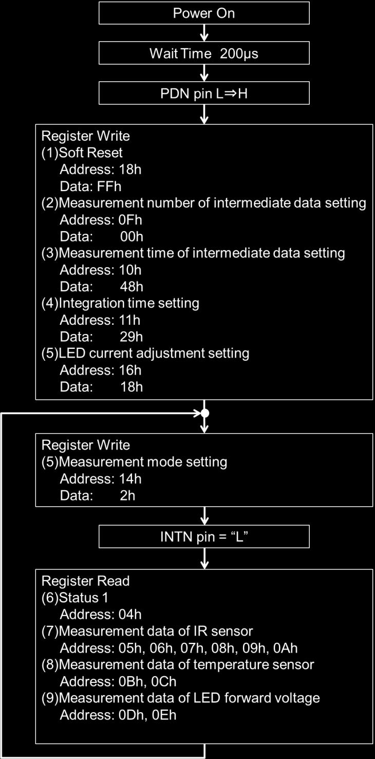
14 11.5. Read Measurement Data After measurement data is set to internal buffer and ready to read, DRDY bit in ST1 register is set to 1. This state is called Data Ready. When the DRDY bit is "1", the output of the INTN pin becomes "L". By the either above ways, it can be confirmed whether Data Ready or not. Readout procedure is described using the measurement example below Readout Procedure (1) Read-out ST1 register DRDY: DRDY shows whether the state is Data Ready or not. DRDY bit = 0 means No Data Ready. DRDY bit = 1 means Data Ready. When DRDY bit = 1, read-out measurement data. (Required Operation) (2) Read-out measurement data Once a data read is initiated from one of the measurement data registers (IR1L to VFH), the AK9721AE recognizes that a data read-out has begun. When a data read-out is initiated, DRDY change to 0. (N-1) (N) (N+1) Stand-by Measurement Stand-by Measurement Stand-by Measurement data register data(n-1) data(n) data(n+1) DRDY INTN pin Read-out data ST1 data(n) ST1 data(n+1) Figure 11.3 Read-out Procedure Example of Read-out Procedure Example of read-out procedure of AK9721AE is shown in the following. The below settings are assumed. Measurement number of intermediate data setting: 1time Measurement time of intermediate data setting: 149ms Integration time setting: 99μs LED current adjustment setting: 100mA Data ready interrupt setting is enable. INTN output turns to L (Active) after completion of data ready
15 - 15 -
16 12. Serial Interface The I 2 C bus interface of the AK9721AE supports standard mode(max, 100kHz) and high speed mode(max. 400kHz) Data Transfer Initially the start condition should be input to access the AK9721AE through the bus. Next, send a one byte slave address, which includes the device address. The AK9721AE compares the slave address, and if these addresses match, the AK9721AE generates an acknowledge signal and executes a Read / Write command. The stop condition should be input after executing a command Changing state of the SDA line The SDA line state should be changed only while the SCL line is L. The SDA line state must be maintained while the SCL line is H. The SDA line state can be changed while the SCL line is H, only when a Start Condition or a Stop Condition is input. SCL SDA Constant Changing Stare Enable Figure 12.1 Changing State of SDA Line Start / Stop Conditions A start condition is generated when the SDA line state is changed from H to L while the SCL line is H. All command start from a start condition. A stop condition is generated when the SDA line state is changed from L to H while the SCL line is H. All command end after a stop condition. SCL SDA Start Condition Figure 12.2 Start / Stop Conditions Stop Condition
17 Acknowledge The device transmitting data will release the SDA line after transmitting one byte of data (SDA line state is H ). The device receiving data will pull the SDA line to L during the next clock. This operation is called Acknowledge. The Acknowledge signal can be used to indicate successful data transfers. The AK9721AE will output an acknowledge signal after receiving a start condition and slave address. The AK9721AE will output an acknowledge signal after receiving each byte, when the write instruction is transmitted. The AK9721AE will transmit the data stored in the selected address after outputting an acknowledge signal, when read instruction is transmitted. Then the AK9721AE will monitor the SDA line after releasing the SDA line. If the master device generates an acknowledge instead of stop condition, the AK9721AE transmits an 8-bit data stored in the next address. When the Acknowledge is not generated, transmitting data is terminated. Clocl pulse for Acknowledge SCL of Master Device Data Output of Transmitter Data Output of Receiver Start Condition Non-Acknowledge Acknowledge Figure 12.3 Acknowledge
18 Slave Address The slave address of the AK9721AE is 65h. MSB LSB R/W Figure 12.4 Slave Address When the first one byte data including the slave address is transmitted after a start condition, the device, which is specified as the communicator by the slave address on bus, selected. After transmitting the slave address, the device that has the corresponding device address will execute a command after transmitting an acknowledge signal. The 8-bit (Least Significant bit-lsb) of the first one byte is the R/W bit. When the R/W bit is set to 1, a READ command is executed. When the R/W bit is set to 0, a WRITE command is executed
19 ACK ACK ACK ACK ACK ACK Start Stop [AK9721AE] WRITE Command When the R/W bit set to 0, the AK9721AE executes a WRITE operation. The AK9721AE will out an acknowledge signal and receive the second byte, after receiving a start condition and first one byte (slave address) in a WRITE operation. The second byte has an MSB-first configuration, and specifies the address of the internal control register. MSB LSB A7 A6 A5 A4 A3 A2 A1 A0 Figure 12.5 Register Address The AK9721AE will generate an acknowledge and receive the third byte after receiving the second byte (register address). The data after the third byte is the control data. The control data consists of 8-bit and has an MSB-first configuration. The AL9721AE generates an acknowledge for each byte received. The data transfer is terminated by a stop condition, generated by the master device. MSB LSB D7 D6 D5 D4 D3 D2 D1 D0 Figure 12.6 Control Data Two or more bytes can be written at once. The AK9721AE generates an acknowledge and receives the next data after receiving the third byte (control data). When the following data is transmitted without a stop condition, after transmitting one byte, the internal address counter is automatically incremented, and data is written in the next address. The automatic increment function works in the address from 0Fh to 17h. When the start address is 0Fh, the address is repeatedly incremented as. 0Fh -> 10h -> -> 17h -> 0Fh -> 10h R/W= 0 SDA S Slave Address Register Address(n) DATA(n) DATA(n+1) DATA(n+x) P Figure 12.7 WRITE Operation
20 ACK ACK ACK ACK ACK ACK Start Start Stop ACK ACK ACK ACK ACK ACK Start Stop [AK9721AE] READ Command When the R/W bit is set to 1, the AK9721AE executes a READ operation. When the AK9721AE transmits data from the specified address, the master device generates an acknowledge instead of a stop condition and the next address data can be read-out. Address can be 00h to 0Eh, 0Fh to 17h. When the address is 00h to 0Eh, the address is incremented 00h -> 01h -> -> 0Eh, and the address goes back to 04h after 0Eh. When the address is 0Fh to17h, the address goes back to 0Fh after 17h. The AK9721AE supports both current address read and random address read. (1) Current Address Read The AK9721AE has an integrated address counter. The data specified by the counter is read-out in the current address read operation. The internal address counter retains the next address which is accessed at last. For example, when the address which was accessed last is n, the data of address n+1 is read-out by the current address read instruction. The AK9721AE will generate an acknowledge after receiving a slave address for a read command (R/W bit = 1 ) in the current address read operation. Then the AK9721AE will start to transmit the data specified by the internal address counter at the next clock, and will increment the internal address counter by one. When the AK9721AE generates a stop condition instead of an acknowledge after transmitting the one byte data, a read-out operation is terminated. R/W= 1 SDA S Slave Address DATA(n) DATA(n+1) DATA(n+2) DATA(n+x) P Figure 12.8 Current Address Read (2) Random Read Data from an arbitrary address can be read-out by a random read operation. A random read requires the input of a dummy WRITE instruction before the input of a slave address of a READ instruction (R/W bit = 1 ). To execute a random read, first generate a start condition, then input the slave address for a WRITE instruction (R/W bit = 0 ) and a read address, sequentially. After the AK9721AE generates an acknowledge in response to this address input, generate a start condition and the slave address for a READ instruction (R/W bit = 1 ) again. The AK9721AE generates an acknowledge in response to the input of this slave address. Next, the AK9721AE output the data at the specified address, then increments the internal address counter by one. When a stop condition from the master device is generated in generated instead of an acknowledge after the AK9721AE outputs data, Read operation stops. R/W= 0 R/W= 1 SDA S Slave Address Register Address(n) Slave S Address DATA(n) DATA(n+1) DATA(n+x) P Figure 12.9 Random Read
21 13. Registers Description of Registers The AK9721AE has registers of 25 addresses as indicated in Table 13.1 Every address consists of 8 bits data. Data is transferred to or received from the external MCU via the serial interface described previously. Table 13.1 Register Table Name Address SRST R/W Data Content bit WIA1 00h Disable R Company Code 8 WIA2 01h Disable R Device ID 8 INFO1 02h Disable R Information 8 INFO2 03h Disable R Information 8 ST1 04h Enable R Status 1 2 IR1L 05h Enable R Measurement data of IR1 (Low) 8 IR1M 06h Enable R Measurement data of IR1 (Middle) 8 IR1H 07h Enable R Measurement data of IR1 (High) 8 IR2L 08h Enable R Measurement data of IR2 (Low) 8 IR2M 09h Enable R Measurement data of IR2 (Middle) 8 IR2H 0Ah Enable R Measurement data of IR2 (High) 8 TMPL 0Bh Enable R Measurement data of temperature sensor(low) 8 TMPH 0Ch Enable R Measurement data of temperature sensor(high) 8 VFL 0Dh Enable R Measurement data of LED forward voltage(low) 8 VFH 0Eh Enable R Measurement data of LED forward voltage (High) 8 CNTL1 0Fh Enable R/W Measurement number of intermediate data 8 CNTL2 10h Enable R/W Measurement time of intermediate data 8 CNTL3 11h Enable R/W Integration time 8 CNTL4 12h Enable R/W IR2 integrated time setting 8 CNTL5 13h Enable R/W INTN pin output setting 2 CNTL6 14h Enable R/W Mode setting 2 CNTL7 15h Enable R/W Detection range switching 7 CNTL8 16h Enable R/W LED current setting 5 CNTL9 17h Enable R/W Resistance measurement mode setting 1 CNTL10 18h Enable R/W Soft reset 1 Addresses 00h to 0Eh, 0Fh to 17h are compliant with automatic increment function of serial interface respectively. When the address is in 00h to 0Eh, the address is incremented 00h -> 01h -> 02h -> -> 0Eh, and the address goes back to 04h after 0Eh. When the address is in 0Fh to 17h, the address goes back to 0Fh after 17h
22 13.2. Register Map 00h WIA h WIA h INFO h INFO h ST ERR_FLAG DRDY 05h IR1L IR1L_7 IR1L_6 IR1L_5 IR1L_4 IR1L_3 IR1L_2 IR1L_1 IR1L_0 06h IR1M IR1M_15 IR1M_14 IR1M_13 IR1M_12 IR1M_11 IR1M_10 IR1M_9 IR1M_8 07h IR1H IR1H_23 IR1H_22 IR1H_21 IR1H_20 IR1H_19 IR1H_18 IR1H_17 IR1H_16 08h IR2L IR2L_7 IR2L_6 IR2L_5 IR2L_4 IR2L_3 IR2L_2 IR2L_1 IR2L_0 09h IR2M IR2M_15 IR2M_14 IR2M_13 IR2M_12 IR2M_11 IR2M_10 IR2M_9 IR2M_8 0Ah IR2H IR2H_23 IR2H_22 IR2H_21 IR2H_20 IR2H_19 IR2H_18 IR2H_17 IR2H_16 0Bh TMPL TMPL_7 TMPL_6 TMPL_5 TMPL_4 TMPL_3 TMPL_2 TMPL_1 TMPL_0 0Ch TMPH TMPH_15 TMPH_14 TMPH_13 TMPH_12 TMPH_11 TMPH_10 TMPH_9 TMPH_8 0Dh VFL VFL_7 VFL_6 VFL_5 VFL_4 VFL_3 VFL_2 VFL_1 VFL_0 0Eh VFH VFH_15 VFH_14 VFH_13 VFH_12 VFH_11 VFH_10 VFH_9 VFH_8 0Fh CNTL1 MLOOP_7 MLOOP_6 MLOOP_5 MLOOP_4 MLOOP_3 MLOOP_2 MLOOP_1 MLOOP_0 10h CNTL2 MTIME_7 MTIME_6 MTIME_5 MTIME_4 MTIME_3 MTIME_2 MTIME_1 MTIME_0 11h CNTL3 ITIME_7 ITIME_6 ITIME_5 ITIME_4 ITIME_3 ITIME_2 ITIME_1 ITIME_0 12h CNTL4 IR2INT_7 IR2INT_6 IR2INT_5 IR2INT_4 IR2INT_3 IR2INT_2 IR2INT_1 IR2INT_0 13h CNTL ERR_DIS DRDY_DIS 14h CNTL MODE_1 MODE_0 15h CNTL7 1 IR2_ MSRIUP IR1_ MSRIUP IR2_SH _GAIN IR1_ADC _RNG IR1_SH _GAIN IR1_AFE _GAIN_1 IR1_AFE _GAIN_0 16h CNTL LEDADJ_4 LEDADJ_3 LEDADJ_2 LEDADJ_1 LEDADJ_0 17h CNTL RES_MEAS 18h CNTL SRST The ERR_FLAG bit is reset in the single measurement mode setting. At this time, the DRDY bit is not reset. The DRDY bit is reset by reading the ST1 register. At this time, the ERR_FLAG bit is not reset
23 13.3. Detailed Description of Register WIA1: Company code 00h WIA Byte fixed code as Company code of AKM WIA2: Device ID 01h WIA Byte fixed code as AKM device ID INFO1, INFO2: Information 02h INFO h INFO INFO1 [7:0]: Reserved register for AKM. INFO2 [7:0]: Reserved register for AKM ST1: Status 1 04h ST1 ERR_FLAG DRDY Reset ERR_FLAG: Error flag 0 : Normal state 1 : Error state The ERR_FLAG bit is "1" when register setting satisfies the following conditions. Error judgment condition: (Integration time) x 18 > (Measurement time) DRDY: Data ready 0 : Normal state 1 : Data ready The DRDY bit turns to 1, when the data is ready to be read. This bit turns back to 0, when either the ST1 register is read
24 IRxL, IRxM, IRxH: Measurement data of IR sensor(x=1,2) 05h IR1L IR1L_7 IR1L_6 IR1L_5 IR1L_4 IR1L_3 IR1L_2 IR1L_1 IR1L_0 06h IR1M IR1M_15 IR1M_14 IR1M_13 IR1M_12 IR1M_11 IR1M_10 IR1M_9 IR1M_8 07h IR1H IR1H_23 IR1H_22 IR1H_21 IR1H_20 IR1H_19 IR1H_18 IR1H_17 IR1H_16 08h IR2L IR2L_7 IR2L_6 IR2L_5 IR2L_4 IR2L_3 IR2L_2 IR2L_1 IR2L_0 09h IR2M IR2M_15 IR2M_14 IR2M_13 IR2M_12 IR2M_11 IR2M_10 IR2M_9 IR2M_8 0Ah IR2H IR2H_23 IR2H_22 IR2H_21 IR2H_20 IR2H_19 IR2H_18 IR2H_17 IR2H_16 Reset Measurement data of IR sensor IR1L[7:0] : IR1 measurement data lower 8-bits IR1M[15:8] : IR1 measurement data middle 8-bits IR1H[23:16] : IR1 measurement data upper 8-bits IR2L[7:0] : IR2 measurement data lower 8-bits IR2M[15:8] : IR2 measurement data middle 8-bits IR2H[23:16] : IR2 measurement data upper 8-bits 24-bit data is stored in two s compliment and little endian format. Table 13.1 Measurement data of IR sensor IRx[23:0] (x=1,2) Hex Decimal IR Sensor output[mv] 7FFFFF x FFFFFF x10-5 EEEEEF AAAAAB TMPL, TMPH: Measurement data of temperature sensor 0Bh TMPL TMPL_7 TMPL_6 TMPL_5 TMPL_4 TMPL_3 TMPL_2 TMPL_1 TMPL_0 0Ch TMPH TMPH_15 TMPH_14 TMPH_13 TMPH_12 TMPH_11 TMPH_10 TMPH_9 TMPH_8 Reset Measurement data of temperature sensor TMPL[7:0] : Temperature data lower 8-bits TMPH[15:8] : Temperature data upper 8-bits 16-bit data is stored in two s compliment and little endian format. By two-point calibration, it is possible to can accurately detect the temperature of -40 ºC to 90 ºC. For details, refer to the application note Calibrating the Temperature sensor
25 Vf: Measurement data of LED forward voltage 0Dh VFL VFL_7 VFL_6 VFL_5 VFL_4 VFL_3 VFL_2 VFL_1 VFL_0 0Eh VFH VFH_15 VFH_14 VFH_13 VFH_12 VFH_11 VFH_10 VFH_9 VFH_8 Reset Measurement data of LED forward voltage VFL[7:0]: Vf data lower 8-bits VFH[15:8]: Vf data upper 8-bits 16-bit data is stored in two s compliment and little endian format. Table 13.3 Measurement data of LED forward voltage Vf[15:0] Hex Decimal LED forward voltage[mv] 7FFF FFFF DDDE BBBC CNTL1: Control1 0Fh CNTL1 MLOOP_7 MLOOP_6 MLOOP_5 MLOOP_4 MLOOP_3 MLOOP_2 MLOOP_1 MLOOP_0 Reset MLOOP[7:0]: Measurement number of intermediate data setting Table 13.4 Measurement number of intermediate data MLOOP[7:0] Hex Decimal Number of measurements[times] FF FE FD
26 CNTL2: Control2 10h CNTL2 MTIME_7 MTIME_6 MTIME_5 MTIME_4 MTIME_3 MTIME_2 MTIME_1 MTIME_0 Reset MTIME[7:0]: Measurement time of intermediate data setting Table 13.5 Measurement time of intermediate data MTIME[7:0] Hex Decimal Measurement time[ms] FF CNTL3: Control3 11h CNTL3 ITIME_7 ITIME_6 ITIME_5 ITIME_4 ITIME_3 ITIME_2 ITIME_1 ITIME_0 Reset ITIME[7:0]: Integration time setting The light emission time of the LED can be obtained by the following formula. LED light emission time = Integration time x [μs] Table 13.6 Integration time ITIME[7:0] Hex Decimal Integration time[μs] FF A
27 CNTL4: Control4 12h CNTL4 IR2INT_7 IR2INT_6 IR2INT_5 IR2INT_4 IR2INT_3 IR2INT_2 IR2INT_1 IR2INT_0 Reset IR2INT[7:0]: Integration time adjustment of IR2 Since the input ranges of IR1 and IR2 are different, the integration time of IR2 can be adjusted to match the measurement range of IR1. The integration time of IR2 is shown below. IR2 integration time = Integration time IR2 mask time[μs] Table 13.7 Integration time adjustment IR2INT[7:0] Hex Decimal IR2mask time [μs] FF
28 CNTL5: Control5 13h CNTL5 ERR_DIS DRDY_DIS Reset DRDY_DIS: DRDY interrupt setting 0 : Enable 1 : Disenable ERR_DIS: Error flag interrupt setting 0 : Enable 1 : Disenable If you do not want to interrupt the HOST from the INTN pin, set the above bit to "1" CNTL6: Control6 14h CNTL6 MODE_1 MODE_0 Reset MODE[1:0]: Measurement mode setting : Stand-by Mode 10 : Single Measurement Mode CNTL7: Control7 IR2_ IR1_ IR2_SH IR1_ADC IR1_SH IR1_AFE IR1_AFE 15h CNTL7 MSRIUP MSRIUP _GAIN _RNG _GAIN _GAIN_1 _GAIN_0 Reset IR1_AFE_GAIN[1:0]: Selection of AFE gain of IR1 measurement path 00 : 2 times 01 : 1 times 10 : 2/3 times 11 : 1/2 times IR1_SH_GAIN: Selection of SH gain of IR1 measurement path 0 : 1 times 1 : 2 times IR1_ADC_RNG: Selection of ADC range of IR1 measurement path 0 : 1000 mv 1 : 500 mv IR2_SH_GAIN: Selection of SH gain of IR2 measurement path 0 : 0.5 times 1 : 0.33 times IR1_MSRIUP: Resolution selection in IR1 resistance measurement mode 0 : 1 times (Measurement range: Maximum 750kΩ) 1 : 4 times (Measurement range: Maximum 187.5kΩ) IR2_MSRIUP: Resolution selection in IR2 resistance measurement mode 0 : 1 times (Measurement range: Maximum 450kΩ) 1 : 4 times (Measurement range: Maximum 112.5kΩ)
29 CNTL8: Control8 16h CNTL8 LEDADJ_4 LEDADJ_3 LEDADJ_2 LEDADJ_1 LEDADJ_0 Reset LEDADJ[4:0]: LED current adjustment Table 13.8 LED current adjustment LEDADJ[4:0] Hex Decimal LED current[ma] 1F E CNTL9: Control9 17h CNTL9 RES_MEAS Reset RES_MEAS: Resistance measurement mode setting 0 : Normal mode 1 : Resistance measurement mode By setting this bit to "1", resistance measurement can be performed by performing single measurement mode CNTL10: Control10 18h CNTL10 SRST Reset SRST: Soft reset 0 : Normal state 1 : Reset All registers are reset by setting SRST bit to 1. SRST bit automatically returns to 0 after reset is activated


30 14. Example of Recommended External Circuits Figure 14.1 Recommended External Circuits Pull-up resistance of SDA, SCL and INTN should be connected to DVDD. Please refer the I 2 C bus specification Ver2.1 and select the suitable resistance value. The resistance value in Figure 14.1 is reference
31 15.1. Outline Dimensions 15. Package Unit: mm Please set the exposed pad to OPEN. Figure 15.1 Outline Dimensions
32 15.2. Pad Dimensions Unit: mm Figure 15.2 Pad Dimensions Do not connect with exposed pad

33 15.3. Marking Y: Year W W: Week L: Lot Mark Year Mark Week Mark Week Mark Lot A B C D E F G H J K L M N P Q R T U V W X Y Z Ordering Guide AK9721AE -40 ~ 90ºC 16-pin QFN Consumer Grade 17. Revision History Date (Y/M/D) Revision Reason Page Contents 17/7/13 00 First Edition
34 IMPORTANT NOTICE 0. Asahi Kasei Microdevices Corporation ( AKM ) reserves the right to make changes to the information contained in this document without notice. When you consider any use or application of AKM product stipulated in this document ( Product ), please make inquiries the sales office of AKM or authorized distributors as to current status of the Products. 1. All information included in this document are provided only to illustrate the operation and application examples of AKM Products. AKM neither makes warranties or representations with respect to the accuracy or completeness of the information contained in this document nor grants any license to any intellectual property rights or any other rights of AKM or any third party with respect to the information in this document. You are fully responsible for use of such information contained in this document in your product design or applications. AKM ASSUMES NO LIABILITY FOR ANY LOSSES INCURRED BY YOU OR THIRD PARTIES ARISING FROM THE USE OF SUCH INFORMATION IN YOUR PRODUCT DESIGN OR APPLICATIONS. 2. The Product is neither intended nor warranted for use in equipment or systems that require extraordinarily high levels of quality and/or reliability and/or a malfunction or failure of which may cause loss of human life, bodily injury, serious property damage or serious public impact, including but not limited to, equipment used in nuclear facilities, equipment used in the aerospace industry, medical equipment, equipment used for automobiles, trains, ships and other transportation, traffic signaling equipment, equipment used to control combustions or explosions, safety devices, elevators and escalators, devices related to electric power, and equipment used in finance-related fields. Do not use Product for the above use unless specifically agreed by AKM in writing. 3. Though AKM works continually to improve the Product s quality and reliability, you are responsible for complying with safety standards and for providing adequate designs and safeguards for your hardware, software and systems which minimize risk and avoid situations in which a malfunction or failure of the Product could cause loss of human life, bodily injury or damage to property, including data loss or corruption. 4. Do not use or otherwise make available the Product or related technology or any information contained in this document for any military purposes, including without limitation, for the design, development, use, stockpiling or manufacturing of nuclear, chemical, or biological weapons or missile technology products (mass destruction weapons). When exporting the Products or related technology or any information contained in this document, you should comply with the applicable export control laws and regulations and follow the procedures required by such laws and regulations. The Products and related technology may not be used for or incorporated into any products or systems whose manufacture, use, or sale is prohibited under any applicable domestic or foreign laws or regulations. 5. Please contact AKM sales representative for details as to environmental matters such as the RoHS compatibility of the Product. Please use the Product in compliance with all applicable laws and regulations that regulate the inclusion or use of controlled substances, including without limitation, the EU RoHS Directive. AKM assumes no liability for damages or losses occurring as a result of noncompliance with applicable laws and regulations. 6. Resale of the Product with provisions different from the statement and/or technical features set forth in this document shall immediately void any warranty granted by AKM for the Product and shall not create or extend in any manner whatsoever, any liability of AKM. 7. This document may not be reproduced or duplicated, in any form, in whole or in part, without prior written consent of AKM. Rev
AK9700AE IR LED for NDIR Gas Sensing
 AK9700AE IR LED for NDIR Gas Sensing 1. General Description The AK9700AE is a small mid-infrared light emitting diode made of AlInSb and optimized for NDIR gas sensing applications. It uses AKM s unique
AK channel Capacitive Touch Sensor IC
 AK4161 6channel Capacitive Touch Sensor IC GENERAL DESCRIPTION The AK4161 is a low operating voltage and low power consumption 6channel capacitive touch sensor. Maximum 6 input channels can be configured
MS-0050 Semiconductor Magnetoresistive Element
 MS-0050 Semiconductor Magnetoresistive Element Semiconductor Magnetoresistive Element Composition MS-0050 is used as rotation sensor for gear (module: m=0.5), combining bias magnet. MS-0050 generates A/B
Ultra Low Power Dual Voltage Detector
 = Preliminary = AP4410BEC Ultra Low Power Dual Voltage Detector 1. General Description The AP4410BEC is a voltage detector IC for monitoring battery, power supply and system voltage. The circuit includes
AK1291 IF Variable Gain Amplifier with RSSI
 AK1291 IF Variable Gain Amplifier with RSSI 1. Overview AK1291 is a variable gain amplifier with a power detector. It s operating frequency ranges from 90MHz to 300MHz. The gain control adopts an analog
Low Power Multiclock Generator with VCXO AK8130AH
 Low Power Multiclock Generator with VCXO Features 27MHz Crystal Input Four Frequency-Selectable Clock Outputs One 27MHz-Reference Output Selectable Clock out Frequencies: - 54.000,74.1758, 74.250MHz -
AP1013CEN. 18V 1ch H-Bridge Motor Driver IC
 AP1013CEN 18V 1ch H-Bridge Motor Driver IC 1. General Description The AP1013CEN realizes four drive mode of forward, reverse, break and standby by 1 channel H-bridge motor driver corresponding to operating
AP V 2ch H-Bridge Motor Driver IC
 1. General Description The AP1040 is a 2ch H-Bridge motor driver that supports a maximum output current of 2.0A and from 8 to 32V operation voltage. The control mode of the AP1040 can be switched between
7.0V Dual H-Bridge Motor Driver IC
 AP1014AEC 7.0V Dual H-Bridge Motor Driver IC 1. Genaral Description The AP1014AEC has four drive mode of forward, reverse, brake and standby by 2 channel H-bridge Motor Driver corresponding to operating
AP V 2ch H-Bridge Motor Driver IC
 AP1010 18V 2ch H-Bridge Motor Driver IC 1. General Description The AP1010 is a 2ch H-Bridge motor driver compatible with motor operating voltage 18V and can drive two DC motors or one stepping motor. The
AP V Dual H-Bridge Motor Driver IC
 1. General Description The AP1018 is a Dual H-Bridge small motor driver corresponding to the motor drive voltage 18V. Since the AP1018 has two output channels, it is capable of driving two DC motors or
TLP3924 TELECOMMUNICATION PROGRAMMABLE CONTROLLERS MOSFET GATE DRIVER. Features. Pin Configuration (top view)
") TOSHIBA PHOTOCOUPLER GaAlAs IRED & PHOTO DIODE ARRAY TELECOMMUNICATION PROGRAMMABLE CONTROLLERS MOSFET GATE DRIVER. Unit: mm φ. The TOSHIBA SSOP coupler is a small outline coupler, suitable for surface
TOSHIBA PHOTOCOUPLER GaAlAs IRED & PHOTO DIODE ARRAY TELECOMMUNICATION PROGRAMMABLE CONTROLLERS MOSFET GATE DRIVER. Unit: mm φ. The TOSHIBA SSOP coupler is a small outline coupler, suitable for surface
AP1013DEN. 18V 1ch H-Bridge Motor Driver IC
 AP1013DEN 18V 1ch H-Bridge Motor Driver IC 1. General Description The AP1013DEN realizes four drive mode of forward, reverse, break and standby by 1 channel H-bridge motor driver corresponding to operating
TLP3902 TLP3902 SOLID STATE RELAY PROGRAMMABLE CONTROLLERS MOSFET GATE DRIVER. Features. Pin Configuration (top view)
") TOSHIBA PHOTOCOUPLER GaAs IRED & PHOTO-DIODE ARRAY TLP92 SOLID STATE RELAY PROGRAMMABLE CONTROLLERS MOSFET GATE DRIVER Unit: mm The TOSHIBA mini flat coupler TLP92 is a small outline coupler, suitable
TOSHIBA PHOTOCOUPLER GaAs IRED & PHOTO-DIODE ARRAY TLP92 SOLID STATE RELAY PROGRAMMABLE CONTROLLERS MOSFET GATE DRIVER Unit: mm The TOSHIBA mini flat coupler TLP92 is a small outline coupler, suitable
TLP206A TLP206A. Measurement Instrument Data Acquisition Programmable Control. Pin Configuration (top view) Internal Circuit
 Internal Circuit") TOSHIBA Photocoupler GaAs IRED & Photo-MOSFET TLP206A Measurement Instrument Data Acquisition Programmable Control Unit: mm The TOSHIBA TLP206A consists of gallium arsenide infrared emitting diode optically
TOSHIBA Photocoupler GaAs IRED & Photo-MOSFET TLP206A Measurement Instrument Data Acquisition Programmable Control Unit: mm The TOSHIBA TLP206A consists of gallium arsenide infrared emitting diode optically
TA75W01FU TA75W01FU. Dual Operational Amplifier. Features Pin Connection (Top View)
") TOSHIBA Bipolar Linear Integrated Circuit Silicon Monolithic TA75W01FU Dual Operational Amplifier Features In the linear mode the input common mode voltage range includes ground. The internally compensated
TOSHIBA Bipolar Linear Integrated Circuit Silicon Monolithic TA75W01FU Dual Operational Amplifier Features In the linear mode the input common mode voltage range includes ground. The internally compensated
TC75W57FU, TC75W57FK
 Dual Comparator TOSHIBA CMOS Linear Integrated Circuit Silicon Monolithic TC75W57FU, TC75W57FK TC75W57FU/FK TC75W57 is a CMOS type general-purpose dual comparator capable of single power supply operation
TLP127 TLP127. Programmable Controllers DC Output Module Telecommunication. Pin Configurations (top view)
") TOSHIBA Photocoupler GaAs Ired & Photo Transistor TLP27 Programmable Controllers DC Output Module Telecommunication Unit: mm The TOSHIBA mini-flat coupler TLP27 is a small outline coupler, suitable for
TOSHIBA Photocoupler GaAs Ired & Photo Transistor TLP27 Programmable Controllers DC Output Module Telecommunication Unit: mm The TOSHIBA mini-flat coupler TLP27 is a small outline coupler, suitable for
TLP206A TLP206A. Measurement Instrument Data Acquisition Programmable Control. Pin Configuration (top view) Internal Circuit
 Internal Circuit") TOSHIBA Photocoupler GaAs IRED & Photo-MOSFET TLP206A Measurement Instrument Data Acquisition Programmable Control Unit: mm The TOSHIBA TLP206A consists of gallium arsenide infrared emitting diode optically
TOSHIBA Photocoupler GaAs IRED & Photo-MOSFET TLP206A Measurement Instrument Data Acquisition Programmable Control Unit: mm The TOSHIBA TLP206A consists of gallium arsenide infrared emitting diode optically
TLP168J TLP168J. Triac Driver Programmable Controllers AC Output Modules Solid State Relays. Pin Configurations
 TLP68J TOSHIBA Photocoupler GaAlAs IRed & Photo-Triac TLP68J Triac Driver Programmable Controllers AC Output Modules Solid State Relays Unit: mm The TOSHIBA mini-flat coupler TLP68J is a small-outline
TLP191B TLP191B. Telecommunication Programmable Controllers MOS Gate Driver MOS FET Gate Driver. TOSHIBA Photocoupler GaAlAs IRED & Photo-Diode Array
 TLP9B TOSHIBA Photocoupler GaAlAs IRED & Photo-Diode Array TLP9B Telecommunication Programmable Controllers MOS Gate Driver MOS FET Gate Driver Unit: mm The TOSHIBA mini-flat coupler TLP9B is a small outline
TLP190B. Telecommunications Programmable Controllers MOS Gate Drivers MOSFET Gate Drivers. Short Current. Pin Configuration (top view)
") TOSHIBA Photocoupler GaAlAs IRED & Photo Diode Array TLP9B Telecommunications Programmable Controllers MOS Gate Drivers MOSFET Gate Drivers Unit: mm The TOSHIBA TLP9B mini-flat photocoupler is suitable
TOSHIBA Photocoupler GaAlAs IRED & Photo Diode Array TLP9B Telecommunications Programmable Controllers MOS Gate Drivers MOSFET Gate Drivers Unit: mm The TOSHIBA TLP9B mini-flat photocoupler is suitable
TOSHIBA Field Effect Transistor Silicon N Channel MOS Type 2SK2009
 TOSHIBA Field Effect Transistor Silicon N Channel MOS Type 2SK2009 High Speed Switching Applications Analog Switch Applications Unit: mm High input impedance. Low gate threshold voltage: V th = 0.5~1.5
TOSHIBA Field Effect Transistor Silicon N Channel MOS Type 2SK1829
 TOSHIBA Field Effect Transistor Silicon N Channel MOS Type 2SK1829 High Speed Switching Applications Analog Switch Applications Unit: mm 2.5 V gate drive Low threshold voltage: V th = 0.5 to 1.5 V High
1. Genaral Description
 AK09970N 3D Magnetic Sensor with Programmable Switch 1. Genaral Description AK09970N is a 3D magnetic sensor IC with high sensitivity and wide measurement range utilizing our latest Hall sensor technology.
HT16C22/HT16C22G RAM Mapping 44 4 LCD Controller Driver
 RAM Mapping 44 4 LCD Controller Driver Features Operating voltage: 2.4V~5.5V Internal 32kHz RC oscillator Bias: 1/2 or 1/3; Duty: 1/4 Internal LCD bias generation with voltage-follower buffers I 2 C-bus
TOSHIBA Field Effect Transistor Silicon N Channel MOS Type SSM3K17FU
 SSMK7FU TOSHIBA Field Effect Transistor Silicon N Channel MOS Type SSMK7FU High Speed Switching Applications Analog Switch Applications Unit: mm Suitable for high-density mounting due to compact package
TOSHIBA Field-Effect Transistor Silicon N-Channel MOS Type SSM3K35MFV. DC I D 180 ma Pulse I DP 360
 SSMKMFV TOSHIBA Field-Effect Transistor Silicon N-Channel MOS Type SSMKMFV High-Speed Switching Applications Analog Switch Applications Unit: mm. V drive Low ON-resistance : R on = Ω (max) (@V GS =. V)
TOSHIBA Field Effect Transistor Silicon N Channel MOS Type SSM3K16FU
 SSMKFU TOSHIBA Field Effect Transistor Silicon N Channel MOS Type SSMKFU High Speed Switching Applications Analog Switching Applications Unit: mm Suitable for high-density mounting due to compact package
TC75S56F, TC75S56FU, TC75S56FE
 TOSHIBA CMOS Linear Integrated Circuit Silicon Monolithic TC75S56F/FU/FE TC75S56F, TC75S56FU, TC75S56FE Single Comparator The TC75S56F/TC75S56FU/TC75S56FE is a CMOS generalpurpose single comparator. The
[AKD570-A] Board Outline Chart Outline Chart J J J JP JP5 JP SW JP JP JP9 J6 T T JP JP JP6 T T JP0 U JP SW JP SW U U JP7 JP8 Port Port J5 J J7 J8 Figu
![[AKD570-A] Board Outline Chart Outline Chart J J J JP JP5 JP SW JP JP JP9 J6 T T JP JP JP6 T T JP0 U JP SW JP SW U U JP7 JP8 Port Port J5 J J7 J8 Figu](/thumbs/90/103721021.jpg "[AKD570-A] Board Outline Chart Outline Chart J J J JP JP5 JP SW JP JP JP9 J6 T T JP JP JP6 T T JP0 U JP SW JP SW U U JP7 JP8 Port Port J5 J J7 J8 Figu") [AKD570-A] AK570 Evaluation Board Rev. GENERA DESCRIPTION AKD570-A is an evaluation board for AK570 which is low voltage bit analog-digital converter developed for digital audio system. It supports Jacks
[AKD570-A] AK570 Evaluation Board Rev. GENERA DESCRIPTION AKD570-A is an evaluation board for AK570 which is low voltage bit analog-digital converter developed for digital audio system. It supports Jacks
TOSHIBA Field Effect Transistor Silicon N Channel Junction Type 2SK mw
 TOSHIBA Field Effect Transistor Silicon N Channel Junction Type Audio Frequency Low Noise Amplifier Applications Unit: mm Including two devices in SM5 (super mini type with 5 leads.) High Y fs : Y fs =
TOSHIBA Field-Effect Transistor Silicon N-Channel MOS Type SSM3K35MFV. DC I D 180 ma Pulse I DP 360
 SSMKMFV TOSHIBA Field-Effect Transistor Silicon N-Channel MOS Type SSMKMFV High-Speed Switching Applications Analog Switch Applications Unit: mm. V drive Low ON-resistance : R on = Ω (max) (@V GS =. V)
TLP170D. PBX Modem Fax Card Telecommunication Security Equipment Measurement Equipment. Pin Configuration (top view) Internal Circuit
 Internal Circuit") TLP7D TOSHIBA Photocoupler GaAs IRED & Photo-MOSFET TLP7D PBX Modem Fax Card Telecommunication Security Equipment Measurement Equipment Unit: mm The Toshiba TLP7D consists of a gallium arsenide infrared
TLP7D TOSHIBA Photocoupler GaAs IRED & Photo-MOSFET TLP7D PBX Modem Fax Card Telecommunication Security Equipment Measurement Equipment Unit: mm The Toshiba TLP7D consists of a gallium arsenide infrared
TOSHIBA Field Effect Transistor Silicon N-Channel Dual Gate MOS Type 3SK292
 TOSHIBA Field Effect Transistor Silicon N-Channel Dual Gate MOS Type 3SK292 TV Tuner, VHF RF Amplifier Application Unit: mm Superior cross modulation performance. Low reverse transfer capacitance: C rss
TLP4227G, TLP4227G-2
 TLP7G,TLP7G- TOSHIBA Photocoupler Photorelay TLP7G, TLP7G- PBX Telecommunication Modem FAX Cards, Modems In PC Measurement Instrumentation TLP7G Unit: mm The TOSHIBA TLP7G series consist of a gallium arsenide
TC7SBL66CFU, TC7SBL384CFU
 TOSHIBA CMOS Digital Integrated Circuit Silicon Monolithic TC7SBL66C,384CFU TC7SBL66CFU, TC7SBL384CFU Low Voltage / Low Capacitance Single Bus Switch The TC7SBL66C and TC7SBL384C are a Low Voltage / Low
TLP4222G,TLP4222G-2 TLP4222G,TLP4222G-2. Telecommunication Measurement Equipment Security Equipment FA. Pin Configuration (top view)
") TOSHIBA Photocoupler Photorelay TLPG,TLPG- TLPG,TLPG- Telecommunication Measurement Equipment Security Equipment FA Unit: mm The Toshiba TLPG consists of an aluminum gallium arsenide infrared emitting
TOSHIBA Photocoupler Photorelay TLPG,TLPG- TLPG,TLPG- Telecommunication Measurement Equipment Security Equipment FA Unit: mm The Toshiba TLPG consists of an aluminum gallium arsenide infrared emitting
TOSHIBA Field Effect Transistor Silicon N-Channel Dual Gate MOS Type 3SK294
 TOSHIBA Field Effect Transistor Silicon N-Channel Dual Gate MOS Type TV Tuner, VHF RF Amplifier Application Unit: mm Superior cross modulation performance Low reverse transfer capacitance: C rss = 20 ff
TLP202A TLP202A. Telecommunications Measurement and Control Equipment Data Acquisition System Measurement Equipment. Pin Configuration (top view)
") TOSHIBA Photocoupler Photorelay TLP22A Telecommunications Measurement and Control Equipment Data Acquisition System Measurement Equipment Unit: mm The Toshiba TLP22A consists of a gallium arsenide infrared
TOSHIBA Photocoupler Photorelay TLP22A Telecommunications Measurement and Control Equipment Data Acquisition System Measurement Equipment Unit: mm The Toshiba TLP22A consists of a gallium arsenide infrared
TOSHIBA Field Effect Transistor Silicon N Channel MOS Type 2SK302
 TOSHIBA Field Effect Transistor Silicon N Channel MOS Type FM Tuner, VHF RF Amplifier Applications Unit: mm Low reverse transfer capacitance: C rss = 0.035 pf (typ.) Low noise figure: NF = 1.7dB (typ.)
TOSHIBA Field Effect Transistor Silicon N Channel MOS Type SSM3K37FS. JEDEC Storage temperature range T stg 55 to 150 C
 TOSHIBA Field Effect Transistor Silicon N Channel MOS Type High Speed Switching Applications Analog Switch Applications Unit: mm.vdrive Low ON-resistance R DS(ON) =.6 Ω (max) (@V GS =. V) R DS(ON) =. Ω
TC4001BP, TC4001BF, TC4001BFT
 TOSHIBA CMOS Digital Integrated Circuit Silicon Monolithic TC4001BP/BF/BFT TC4001BP, TC4001BF, TC4001BFT TC4001B Quad 2 Input NOR Gate The TC4001B is 2-input positive NOR gate, respectively. Since the
TLP523, TLP523 2, TLP523 4
 TLP,TLP,TLP 4 TOSHIBA Photocoupler GaAs Ired & Photo Transistor TLP, TLP, TLP 4 Programmable Controllers DC Output Module Solid State Relay Unit: mm The TOSHIBA TLP, and 4 consist of a gallium arsenide
TLX9185A. Pin Configuration TOSHIBA Photocoupler IRLED & Photo-Transistor. Unit: mm
 TLX985A TOSHIBA Photocoupler IRLED & Photo-Transistor TLX985A 〇 Various Controllers 〇 Signal transmission between different circuit potential 〇 HEV (Hybrid Electric Vehicle) and EV (Electric Vehicle) Applications
TC7MBL3245AFT, TC7MBL3245AFK
 TOSHIBA CMOS Digital Integrated Circuit Silicon Monolithic TC7MBL3245AFT/FK TC7MBL3245AFT, TC7MBL3245AFK Octal Low Voltage Bus Switch The TC7MBL3245A provides eight bits of low-voltage, high-speed bus
TOSHIBA Photocoupler GaAs IRED & Photo-Triac TLP161J. Marking of Classification
 TOSHIBA Photocoupler GaAs IRED & Photo-Triac TLP161J Triac Drive Programmable Controllers AC-Output Module Solid State Relay Unit: mm The TOSHIBA mini flat coupler TLP161J is a small outline coupler, suitable
TLP176D TLP176D. Modem in PC Modem Fax Card Telecommunication. Pin Configuration (top view) Internal Circuit
 Internal Circuit") TLP76D TOSHIBA Photocoupler GaAs IRED & Photo-MOSFET TLP76D Modem in PC Modem Fax Card Telecommunication Unit: mm The TOSHIBA TLP76D consists of gallium arsenide infrared emitting diode optically coupled
TLP76D TOSHIBA Photocoupler GaAs IRED & Photo-MOSFET TLP76D Modem in PC Modem Fax Card Telecommunication Unit: mm The TOSHIBA TLP76D consists of gallium arsenide infrared emitting diode optically coupled
SSM6K202FE SSM6K202FE. High-Speed Switching Applications Power Management Switch Applications. Absolute Maximum Ratings (Ta = 25 C)
") SSM6K22FE TOSHIBA Field-Effect Transistor Silicon N-Channel MOS Type SSM6K22FE High-Speed Switching Applications Power Management Switch Applications.8 V drive Low ON-resistance: R on = 4 mω (max) (@V
SSM6K22FE TOSHIBA Field-Effect Transistor Silicon N-Channel MOS Type SSM6K22FE High-Speed Switching Applications Power Management Switch Applications.8 V drive Low ON-resistance: R on = 4 mω (max) (@V
TOSHIBA Field-Effect Transistor Silicon N Channel MOS Type SSM3K7002F
 SSMK7F TOSHIBA Field-Effect Transistor Silicon N Channel MOS Type SSMK7F High-Speed Switching Applications Analog Switch Applications Unit: mm Small package Low ON-resistance : R on =. Ω (max) (@V GS =.
TOSHIBA Field Effect Transistor Silicon N Channel MOS Type SSM3K15FV
 SSMKFV TOSHIBA Field Effect Transistor Silicon N Channel MOS Type SSMKFV High Speed Switching Applications Analog Switch Applications Unit: mm Optimum for high-density mounting in small packages Low on-resistance
SSM3K36FS N X SSM3K36FS. High-Speed Switching Applications. Equivalent Circuit (top view) Absolute Maximum Ratings (Ta = 25 C)
 Absolute Maximum Ratings (Ta = 25 C)") TOSHIBA Field-Effect Transistor Silicon N Channel MOS Type High-Speed Switching Applications.5-V drive Low ON-resistance : R on =.5 Ω (max) (@V GS =.5 V) : R on =.4 Ω (max) (@V GS =.8 V) : R on =.85 Ω
TOSHIBA Field-Effect Transistor Silicon N Channel MOS Type High-Speed Switching Applications.5-V drive Low ON-resistance : R on =.5 Ω (max) (@V GS =.5 V) : R on =.4 Ω (max) (@V GS =.8 V) : R on =.85 Ω
TLP174GA TLP174GA. Modem Fax Cards, Modems in PC Telecommunications PBX Measurement Equipment. Pin Configuration (top view)
") TLP7GA TOSHIBA Photocoupler Photorelay TLP7GA Modem Fax Cards, Modems in PC Telecommunications PBX Measurement Equipment Unit: mm The Toshiba TLP7GA consists of an aluminum gallium arsenide infrared emitting
TLP7GA TOSHIBA Photocoupler Photorelay TLP7GA Modem Fax Cards, Modems in PC Telecommunications PBX Measurement Equipment Unit: mm The Toshiba TLP7GA consists of an aluminum gallium arsenide infrared emitting
TLP202A TLP202A. Telecommunications Measurement and Control Equipment Data Acquisition System Measurement Equipment. Pin Configuration (top view)
") TOSHIBA Photocoupler Photorelay TLP22A Telecommunications Measurement and Control Equipment Data Acquisition System Measurement Equipment Unit: mm The Toshiba TLP22A consists of a gallium arsenide infrared
TOSHIBA Photocoupler Photorelay TLP22A Telecommunications Measurement and Control Equipment Data Acquisition System Measurement Equipment Unit: mm The Toshiba TLP22A consists of a gallium arsenide infrared
TLP222A, TLP222A-2 TLP222A,TLP222A-2. Telecommunications Measurement and Control Equipment Data Acquisition System Measurement Equipment
 TOSHIBA Photocoupler Photorelay TLPA, TLPA- TLPA,TLPA- Telecommunications Measurement and Control Equipment Data Acquisition System Measurement Equipment Unit: mm TLPA The Toshiba TLPA and TLPA- consist
TLP3542 TLP3542 TESTERS DATA RECORDING EQUIPMENTS MEASUREMENT EQUIPMENTS. Pin Configuration (top view) Schematic
 Schematic") TLP5 TOSHIBA PHOTOCOUPLER PHOTO RELAY TLP5 TESTERS DATA RECORDING EQUIPMENTS MEASUREMENT EQUIPMENTS Unit: mm The TOSHIBA TLP5 consist of a aluminum gallium arsenide infrared emitting diode optically coupled
TLP5 TOSHIBA PHOTOCOUPLER PHOTO RELAY TLP5 TESTERS DATA RECORDING EQUIPMENTS MEASUREMENT EQUIPMENTS Unit: mm The TOSHIBA TLP5 consist of a aluminum gallium arsenide infrared emitting diode optically coupled
RN4987 RN4987. Switching, Inverter Circuit, Interface Circuit and Driver Circuit Applications. Equivalent Circuit and Bias Resister Values
 TOSHIBA Transistor Silicon NPN/PNP Epitaxial Type (PCT Process) (Transistor with Built-in Bias Resistor) RN4987 RN4987 Switching, Inverter Circuit, Interface Circuit and Driver Circuit Applications Unit:
TLP550 TLP550. Digital Logic Isolation Line Receiver Feedback Control Power Supply Control Switching Power Supply Transistor Inverter
 TLP TOSHIBA Photocoupler Infrared LED + Photo IC TLP Digital Logic Isolation Line Receiver Feedback Control Power Supply Control Switching Power Supply Transistor Inverter Unit: mm TLP constructs a high
TLP176D TLP176D. Modem in PC Modem Fax Card Telecommunication. Pin Configuration (top view) Internal Circuit
 Internal Circuit") TLP76D TOSHIBA Photocoupler GaAs IRED & Photo-MOSFET TLP76D Modem in PC Modem Fax Card Telecommunication Unit: mm The TOSHIBA TLP76D consists of gallium arsenide infrared emitting diode optically coupled
TLP76D TOSHIBA Photocoupler GaAs IRED & Photo-MOSFET TLP76D Modem in PC Modem Fax Card Telecommunication Unit: mm The TOSHIBA TLP76D consists of gallium arsenide infrared emitting diode optically coupled
TLP3122 TLP3122. Measurement Instruments Logic Testers / Memory Testers Board Testers / Scanners Power Line Control FA (Factory Automation) Features
 Features") TLP22 TOSHIBA Photocoupler PHOTORELAY TLP22 Measurement Instruments Logic Testers / Memory Testers Board Testers / Scanners Power Line Control FA (Factory Automation) Unit: mm The TOSHIBA TLP22 consists
TLP22 TOSHIBA Photocoupler PHOTORELAY TLP22 Measurement Instruments Logic Testers / Memory Testers Board Testers / Scanners Power Line Control FA (Factory Automation) Unit: mm The TOSHIBA TLP22 consists
TOSHIBA Field Effect Transistor Silicon P Channel MOS Type 2SJ200
 TOSHIBA Field Effect Transistor Silicon P Channel MOS Type High Power Amplifier Application Unit: mm High breakdown voltage : V DSS = 180 V High forward transfer admittance : Y fs = 4.0 S (typ.) Complementary
TC7SB66CFU, TC7SB67CFU
 TOSHIBA CMOS Digital Integrated Circuit Silicon Monolithic TC7SB66CFU, TC7SB67CFU TC7SB66C,67CFU Low Capacitance Single Bus Switch (analog) The TC7SB66C and TC7SB67C are low ON-resistance, high-speed CMOS
TOSHIBA Field-Effect Transistor Silicon N-Channel MOS Type SSM3K37MFV. ma Pulse I DP 500
 SSMK7MFV TOSHIBA Field-Effect Transistor Silicon N-Channel MOS Type SSMK7MFV High Speed Switching Applications Analog Switch Applications nit: mm.-v drive Low ON-resistance R DS(ON) =.6Ω (max) (@V GS =.
TC75S55F, TC75S55FU, TC75S55FE
 TOSHIBA CMOS Linear Integrated Circuit Silicon Monolithic TC7SF/FU/FE TC7SF, TC7SFU, TC7SFE Single Operational Amplifier The TC7SF/TC7SFU/TC7SFE is a CMOS singleoperation amplifier which incorporates a
TOSHIBA Field Effect Transistor Silicon P Channel MOS Type SSM3J01T. A Pulse. 3.4 (Note 2) 1250 mw
 1250 mw") SSMJT TOSHIBA Field Effect Transistor Silicon P Channel MOS Type SSMJT Power Management Switch High Speed Switching Applications Unit: mm Small Package Low on Resistance : R on =.4 Ω (max) (@V GS = ) :
SSMJT TOSHIBA Field Effect Transistor Silicon P Channel MOS Type SSMJT Power Management Switch High Speed Switching Applications Unit: mm Small Package Low on Resistance : R on =.4 Ω (max) (@V GS = ) :
TLP160G TLP160G. Triac Drive Programmable Controllers AC-Output Module Solid State Relay. Pin Configurations (top view) Trigger LED Current
 Trigger LED Current") TOSHIBA Photocoupler GaAs Ired & Photo-Triac Triac Drive Programmable Controllers AC-Output Module Solid State Relay Unit: mm The TOSHIBA mini flat coupler is a small outline coupler, suitable for surface
TOSHIBA Photocoupler GaAs Ired & Photo-Triac Triac Drive Programmable Controllers AC-Output Module Solid State Relay Unit: mm The TOSHIBA mini flat coupler is a small outline coupler, suitable for surface
TOSHIBA Transistor Silicon NPN Epitaxial Type (PCT Process) RN1110MFV,RN1111MFV
 RN1110MFV,RN1111MFV") RN0MFV,RNMFV TOSHIBA Transistor Silicon NPN Epitaxial Type (PCT Process) RN0MFV,RNMFV Switching, Inverter Circuit, Interface Circuit and Driver Circuit Applications Ultra-small package, suited to very
RN0MFV,RNMFV TOSHIBA Transistor Silicon NPN Epitaxial Type (PCT Process) RN0MFV,RNMFV Switching, Inverter Circuit, Interface Circuit and Driver Circuit Applications Ultra-small package, suited to very
TOSHIBA Transistor Silicon NPN Epitaxial Type (PCT process) 2SC2240
 2SC2240") TOSHIBA Transistor Silicon NPN Epitaxial Type (PCT process) 2SC2240 Low Noise Audio Amplifier Applications Unit: mm The 2SC2240 is a transistor for low frequency and low noise applications. This device
TOSHIBA Transistor Silicon NPN Epitaxial Type (PCT process) 2SC2240 Low Noise Audio Amplifier Applications Unit: mm The 2SC2240 is a transistor for low frequency and low noise applications. This device
1. Genaral Description
 AP1150ADSXX 14V Input / 200mA Output LDO Regulator 1. Genaral Description The AP1150ADSxx is a low dropout linear regulator with ON/OFF control, which can supply 200mA load current. The IC is an integrated
TLP504A,TLP504A 2. Programmable Controllers AC / DC Input Module Solid State Relay. Pin Configurations (top view)
") TOSHIBA Photocoupler GaAs Ired & Photo Transistor TLP4A,TLP4A 2 TLP4A,TLP4A 2 Programmable Controllers AC / DC Input Module Solid State Relay Unit in mm The TOSHIBA TLP4A and TLP4A 2 consists of a photo
TOSHIBA Photocoupler GaAs Ired & Photo Transistor TLP4A,TLP4A 2 TLP4A,TLP4A 2 Programmable Controllers AC / DC Input Module Solid State Relay Unit in mm The TOSHIBA TLP4A and TLP4A 2 consists of a photo
TLP172A. Telecommunications Control Equipment Data Acquisition System Security Equipment Measurement Equipment. Pin Configuration (top view)
") TOSHIBA Photocoupler Photorelay Telecommunications Control Equipment Data Acquisition System Security Equipment Measurement Equipment Unit: mm The Toshiba consists of a gallium arsenide infrared emitting
TOSHIBA Photocoupler Photorelay Telecommunications Control Equipment Data Acquisition System Security Equipment Measurement Equipment Unit: mm The Toshiba consists of a gallium arsenide infrared emitting
Pin Assignment SEG28 SEG29 SEG30 SEG31 SEG32 SEG33 SEG34 SEG35 SEG36 SEG37 SEG38 VDD SDA SCL COM0 COM1 COM2 COM3 COM4 COM5 COM6 COM
 General Description Features VK2C23 56 4 / 52 8 LCD Driver Controller The VK2C23 device is a memory mapping and multi-function LCD controller driver. The Display segments of the device are 224 patterns
TLP227G, TLP227G 2 TLP227G,TLP227G 2. Cordless Telephone PBX Modem. Pin Configuration (top view) Internal Circuit (TLP227G)
 Internal Circuit (TLP227G)") TOSHIBA Photocoupler Photo Relay, Cordless Telephone PBX Modem, Unit: mm The TOSHIBA series consist of a gallium arsenide infrared emitting diode optically coupled to a photo MOS FET in a plastic DIP package.
TOSHIBA Photocoupler Photo Relay, Cordless Telephone PBX Modem, Unit: mm The TOSHIBA series consist of a gallium arsenide infrared emitting diode optically coupled to a photo MOS FET in a plastic DIP package.
TLP160G TLP160G. Triac Drive Programmable Controllers AC Output Module Solid State Relay. Trigger LED Current. Pin Configurations
 TLP60G TOSHIBA Photocoupler GaAs Ired & Photo-Triac TLP60G Triac Drive Programmable Controllers AC Output Module Solid State Relay Unit in mm The TOSHIBA mini flat coupler TLP60G is a small outline coupler,
HT16C23/HT16C23G RAM Mapping 56 4 / 52 8 LCD Driver Controller
 RAM Mapping 56 4 / 52 8 LCD Driver Controller Features Operating voltage: 2.4 ~ 5.5V Internal 32kHz RC oscillator Bias: 1/3 or 1/4; Duty:1/4 or 1/8 Internal LCD bias generation with voltage-follower buffers
TOSHIBA Transistor Silicon NPN Epitaxial Type (PCT process) 2SC4213
 2SC4213") TOSHIBA Transistor Silicon NPN Epitaxial Type (PCT process) 2SC4213 For Muting and Switching Applications Unit: mm High emitter-base voltage: V EBO = 25 V (min) High reverse h FE : Reverse h FE = 150 (typ.)
TOSHIBA Transistor Silicon NPN Epitaxial Type (PCT process) 2SC4213 For Muting and Switching Applications Unit: mm High emitter-base voltage: V EBO = 25 V (min) High reverse h FE : Reverse h FE = 150 (typ.)
TC4069UBP, TC4069UBF, TC4069UBFT
 TOSHIBA CMOS Digital Integrated Circuit Silicon Monolithic TC4069UBP/UBF/UBFT TC4069UBP, TC4069UBF, TC4069UBFT TC4069UB Hex Inverter TC4069UB contains six circuits of inverters. Since the internal circuit
TLP559(IGM) TLP559(IGM) Transistor Inverters Air Conditioner Inverters Line Receivers Intelligent Power Modules (IPMs) Interfaces
 TLP559(IGM) Transistor Inverters Air Conditioner Inverters Line Receivers Intelligent Power Modules (IPMs) Interfaces") TOSHIBA Photocoupler GaAlAs Ired & Photo IC TLP559(IGM) Transistor Inverters Air Conditioner Inverters Line Receivers Intelligent Power Modules (IPMs) Interfaces Unit: mm The TOSHIBA TLP559(IGM) consists
TOSHIBA Photocoupler GaAlAs Ired & Photo IC TLP559(IGM) Transistor Inverters Air Conditioner Inverters Line Receivers Intelligent Power Modules (IPMs) Interfaces Unit: mm The TOSHIBA TLP559(IGM) consists
TOSHIBA Field Effect Transistor Silicon P Channel MOS Type (U-MOSⅥ) TPC8120
 TPC8120") TPC82 TOSHIBA Field Effect Transistor Silicon P Channel MOS Type (U-MOSⅥ) TPC82 Lithium Ion Battery Applications Power Management Switch Applications Unit: mm Small footprint due to small and thin package
TPC82 TOSHIBA Field Effect Transistor Silicon P Channel MOS Type (U-MOSⅥ) TPC82 Lithium Ion Battery Applications Power Management Switch Applications Unit: mm Small footprint due to small and thin package
SSM3J118TU SSM3J118TU. High-Speed Switching Applications. Absolute Maximum Ratings (Ta = 25 C) Electrical Characteristics (Ta = 25 C)
 Electrical Characteristics (Ta = 25 C)") TOSHIBA Field-Effect Transistor Silicon P-Channel MOS Type High-Speed Switching Applications 4 V drive Low ON-resistance: R on = 48 mω (max) (@V GS = 4 V) R on = 24 mω (max) (@V GS = V) Absolute Maximum
TOSHIBA Field-Effect Transistor Silicon P-Channel MOS Type High-Speed Switching Applications 4 V drive Low ON-resistance: R on = 48 mω (max) (@V GS = 4 V) R on = 24 mω (max) (@V GS = V) Absolute Maximum
TOSHIBA Field Effect Transistor Silicon N Channel MOS Type (L 2 -π-mos V) 2SK2963
 2SK2963") TOSHIBA Field Effect Transistor Silicon N Channel MOS Type (L 2 -π-mos V) 2SK2963 2SK2963 DC-DC Converter, Relay Drive and Motor Drive Applications Unit: mm 4-V gate drive Low drain-source ON-resistance:
TOSHIBA Field Effect Transistor Silicon N Channel MOS Type (L 2 -π-mos V) 2SK2963 2SK2963 DC-DC Converter, Relay Drive and Motor Drive Applications Unit: mm 4-V gate drive Low drain-source ON-resistance:
SSM3K35CTC SSM3K35CTC. 1. Applications. 2. Features. 3. Packaging and Pin Assignment Rev.3.0. Silicon N-Channel MOS
 MOSFETs Silicon N-Channel MOS 1. Applications High-Speed Switching Analog Switches 2. Features (1) 1.2-V gate drive voltage. (2) Low drain-source on-resistance = 9.0 Ω (max) (@V GS = 1.2 V, I D = 10 ma)
Toshiba Intelligent Power Device Silicon Monolithic Power MOS Integrated Circuit TPD1036F
 Toshiba Intelligent Power Device Silicon Monolithic Power MOS Integrated Circuit TPD6F -IN- Low-Side Power Switch for Motor, Solenoid and Lamp Drivers TPD6F The TPD6F is a -IN- low-side switch. The output
TOSHIBA Field Effect Transistor Silicon P Channel MOS Type SSM3J36FS
 SSMJ6FS TOSHIBA Field Effect Transistor Silicon P Channel MOS Type SSMJ6FS Power Management Switches.-V drive Low ON-resistance: R on =.6 Ω (max) (@V GS = -. V) : R on =.7 Ω (max) (@V GS = -.8 V) : R on
TLP206G TLP206G. PBX Modem FAX Card Measurement Instrument. Pin Configuration (top view) TOSHIBA Photocoupler GaAs Ired & Photo-MOS FET
 TOSHIBA Photocoupler GaAs Ired & Photo-MOS FET") TLP26G PBX Modem FAX Card Measurement Instrument TOSHIBA Photocoupler GaAs Ired & Photo-MOS FET TLP26G Unit: mm The TOSHIBA TLP26G consists of gallium arsenide infrared emitting diode optically coupled
TLP26G PBX Modem FAX Card Measurement Instrument TOSHIBA Photocoupler GaAs Ired & Photo-MOS FET TLP26G Unit: mm The TOSHIBA TLP26G consists of gallium arsenide infrared emitting diode optically coupled
TOSHIBA Photocoupler GaAs Ired & Photo-Transistor TLP124
 TLP24 TOSHIBA Photocoupler GaAs Ired & Photo-Transistor TLP24 Programmable Controllers AC / DC-Input Module Solid-State Relays Unit: mm The TOSHIBA mini flat coupler TLP24 is a small outline coupler, suitable
HN1B01F HN1B01F. Audio-Frequency General-Purpose Amplifier Applications Q1: Q2: Marking. Q1 Absolute Maximum Ratings (Ta = 25 C)
") TOSHIBA Transistor Silicon PNP Epitaxial Type (PCT Process) Silicon NPN Epitaxial Type (PCT Process) Audio-Frequency General-Purpose Amplifier Applications Q1: High voltage and high current : VCEO = 50
TOSHIBA Transistor Silicon PNP Epitaxial Type (PCT Process) Silicon NPN Epitaxial Type (PCT Process) Audio-Frequency General-Purpose Amplifier Applications Q1: High voltage and high current : VCEO = 50
SSM3K357R SSM3K357R. 1. Applications. 2. Features. 3. Packaging and Pin Assignment Rev.2.0. Silicon N-Channel MOS.
 MOSFETs Silicon N-Channel MOS SSM3K357R SSM3K357R 1. Applications Relay Drivers 2. Features (1) AEC-Q101 Qualified (Note1). (2) 3.0-V gate drive voltage. (3) Built-in Internal Zener diodes and resistors.
TPCC8103 TPCC8103. Notebook PC Applications Portable Equipment Applications. Absolute Maximum Ratings (Ta = 25 C) Circuit Configuration
 Circuit Configuration") TOSHIBA Field Effect Transistor Silicon P-Channel MOS Type (U-MOSⅤ) TPCC83 TPCC83 Notebook PC Applications Portable Equipment Applications Unit: mm Small footprint due to a small and thin package Low drain-source
TOSHIBA Field Effect Transistor Silicon P-Channel MOS Type (U-MOSⅤ) TPCC83 TPCC83 Notebook PC Applications Portable Equipment Applications Unit: mm Small footprint due to a small and thin package Low drain-source
TOSHIBA Field Effect Transistor Silicon N-Channel MOS Type (U-MOSⅥ-H) TPCA8048-H
 TPCA8048-H") TOSHIBA Field Effect Transistor Silicon N-Channel MOS Type (U-MOSⅥ-H) Switching Regulator Applications Motor Drive Applications DC-DC Converter Applications.7. ±. 8 5.5 M A Unit: mm Small footprint due
TOSHIBA Field Effect Transistor Silicon N-Channel MOS Type (U-MOSⅥ-H) Switching Regulator Applications Motor Drive Applications DC-DC Converter Applications.7. ±. 8 5.5 M A Unit: mm Small footprint due
TC7MBL3257CFT,TC7MBL3257CFK,TC7MBL3257CFTG
 TOSHIBA CMOS Digital Integrated Circuit Silicon Monolithic TC7MBL3257CFT/FK/FTG TC7MBL3257CFT,TC7MBL3257CFK,TC7MBL3257CFTG 4-Bit 1-of-2 Multiplexer/Demultiplexer The TC7MBL3257C is a Low Voltage/Low Capacitance
TOSHIBA Field Effect Transistor Silicon P Channel MOS Type (U-MOSⅥ) TPC8120
 TPC8120") TOSHIBA Field Effect Transistor Silicon P Channel MOS Type (U-MOSⅥ) Lithium Ion Battery Applications Power Management Switch Applications Unit: mm Small footprint due to small and thin package Low drain-source
TOSHIBA Field Effect Transistor Silicon P Channel MOS Type (U-MOSⅥ) Lithium Ion Battery Applications Power Management Switch Applications Unit: mm Small footprint due to small and thin package Low drain-source
TLP560J TLP560J. Triac Driver Programmable Controllers AC Output Module Solid State Relay. Pin Configuration (top view)
") TLP6J TOSHIBA Photocoupler GaAs Ired & Photo Triac TLP6J Triac Driver Programmable Controllers AC Output Module Solid State Relay Unit in mm The TOSHIBA TLP6J consists of a photo triac optically coupled
TLP6J TOSHIBA Photocoupler GaAs Ired & Photo Triac TLP6J Triac Driver Programmable Controllers AC Output Module Solid State Relay Unit in mm The TOSHIBA TLP6J consists of a photo triac optically coupled
TOSHIBA Field Effect Transistor Silicon N Channel Junction Type 2SK211. Characteristics Symbol Test Condition Min Typ. Max Unit
 TOSHIBA Field Effect Transistor Silicon N Channel Junction Type FM Tuner Applications VHF Band Amplifier Applications Unit: mm Low noise figure: NF = 2.5dB (typ.) (f = 100 MHz) High forward transfer admitance:
TC7W00FU, TC7W00FK TC7W00FU/FK. Dual 2-Input NAND Gate. Features. Marking. Pin Assignment (top view)
") TOSHIBA CMOS Digital Integrated Circuit Silicon Monolithic TC7W00FU, TC7W00FK TC7W00FU/FK Dual 2-Input NAND Gate Features High Speed : t pd = 6ns (typ.) at V CC = 5V Low power dissipation : I CC = 1μA
TOSHIBA CMOS Digital Integrated Circuit Silicon Monolithic TC7W00FU, TC7W00FK TC7W00FU/FK Dual 2-Input NAND Gate Features High Speed : t pd = 6ns (typ.) at V CC = 5V Low power dissipation : I CC = 1μA
RN2101MFV, RN2102MFV, RN2103MFV RN2104MFV, RN2105MFV, RN2106MFV
 RN21MFV TOSHIBA Transistor Silicon PNP Epitaxial Type (PCT Process) (Bias Resistor built-in Transistor) RN21MFV, RN22MFV, RN23MFV,, Switching, Inverter Circuit, Interface Circuit and Driver Circuit Applications
TC7WH00FU, TC7WH00FK
 Dual 2-Input NAND Gate TOSHIBA CMOS Digital Integrated Circuit Silicon Monolithic TC7WH00FU, TC7WH00FK TC7WH00FU/FK Features High speed operation : t pd = 3.7ns (typ.) at V CC = 5 V, CL = 15pF Low power
Low-Current Consumption, Real-Time Clock IC (General-Purpose IC)
") S1T542XXD0A00 Low-Current Consumption, Real-Time Clock IC (General-Purpose IC) Operating power voltage 1.6 to 5.5V (-40 to +85 C) Output control 32.768kHz output function Clock power voltage 1.2 to 5.5V
S1T542XXD0A00 Low-Current Consumption, Real-Time Clock IC (General-Purpose IC) Operating power voltage 1.6 to 5.5V (-40 to +85 C) Output control 32.768kHz output function Clock power voltage 1.2 to 5.5V
TC7S04FU. Inverter. Features. Absolute Maximum Ratings (Ta = 25 C) TOSHIBA CMOS Digital Integrated Circuit Silicon Monolithic
 TOSHIBA CMOS Digital Integrated Circuit Silicon Monolithic") TOSHIBA CMOS Digital Integrated Circuit Silicon Monolithic TC7S04F, TC7S04FU Inverter The TC7S04 is a high speed C 2 MOS Inverter fabricated with silicon gate C 2 MOS technology. It achieves high speed
TOSHIBA CMOS Digital Integrated Circuit Silicon Monolithic TC7S04F, TC7S04FU Inverter The TC7S04 is a high speed C 2 MOS Inverter fabricated with silicon gate C 2 MOS technology. It achieves high speed
TLP3123 TLP3123. Measurement Instruments Power Line Control FA (Factory Automation) Features. Pin configuration (top view) Schematic
 Features. Pin configuration (top view) Schematic") TLP TOSHIBA Photocoupler PHOTORELAY TLP Measurement Instruments Power Line Control FA (Factory Automation) Unit: mm The TOSHIBA TLP consists of a gallium arsenide infrared emitting diode optically coupled
TLP TOSHIBA Photocoupler PHOTORELAY TLP Measurement Instruments Power Line Control FA (Factory Automation) Unit: mm The TOSHIBA TLP consists of a gallium arsenide infrared emitting diode optically coupled