High Voltage Power MOSFET & IGBTs. Ester Spitale
|
|
|
- Arthur Cannon
- 5 years ago
- Views:
Transcription

1 High Voltage Power MOSFET & IGBTs Ester Spitale


2 ST HV Power MOSFETs: WW most complete offer 1500V 1000V 800V 600V 500V SuperMESH NK SuperMESH 3 K3 MDmesh II SuperMESH 5 K5 MDmesh V 200V Planar Super-junction Normalised R DS(on) x Area
3 ST Power MOSFET s: Nomenclature 3 ST x 42 N 65 M5 C = TSSOP8 T = SOT23-6L H = H 2 PAK (2 to 7 leads) R = PPAK Z = P 2 PAK Y= Max247 E = ISOTOP Q = TO-92 FW = TO-3PF N = SOT-223 L = PowerFLAT U = IPAK I = I 2 PAK S = SO-8 D = DPAK B = D 2 PAK P = TO-220/Pentawatt F = TO-220FP W = TO-247 PACKAGE INDICATIVE CURRENT RANGE BREAKDOWN VOLTAGE 10 (with the exception of non 10 multiples) CHANNEL POLARITY TECHNOLOGY SPECIAL FEATURES M5 = MDmesh V >200V K3 = SuperMESH3 >300V K5 = SuperMESH5 >900V up to 1500V T = Temperature Sensing C = Current Sensing Z = Clamped by Zener Diode V D = Fast Recovery Diode N = N- Channel P = P-Channel NS or PS = N-Ch or P-Ch plus Schottky Diode (electrically connected, monolithic included) DNS or DPS = N-Ch or P-Ch plus Schottky Diode (not electrically connected) N N = Two different N-Channel dice N P = Complementary pair DN or DP = Dual N-Ch or Dual P-Ch Insert All the TM
4 HV MOSFETs: 500V 700V


5 SuperMESH3 Abs. Max Ratings STD planar SuperMESH 3 V DSS 400V,450V,500V, 600V 400V,450V,525V, 600V,620V,650V Diode dv/dt, di/dt 4.5V/ns, 400A/µs Up to 12 V/ns,400A/µs V th 3V 4.5V 3V 4.5V P Source D.E. Substrate Body P Higher margin & robustness Higher ESD immunity HIGHER V DSS BtB G-S Zeners Higher dv/dt REDUCED Trr Improved DYNAMIC (Qg Ciss, Crss) Lower switching losses
 planar")
6 SuperMESH3 Improved dynamic SuperMESH3 Vs equivalent planar device Ciss Coss Crss SuperMESH Other Planar (similar R dson ) Device: STx6N62K3 Conditions : Vds=25V ; f=1mhz ; Vgs=0V ; Tj=25 C SuperMESH3 Features Lower Gate Charge Benefits Lower Switching losses Lower gate driving losses Same R DS(on) planar techno
 State-of-the-art MDmesh V MDmesh II Best")
7 Why use an ST HV Power MOSFETs!! R DS(on) State-of-the-art MDmesh V MDmesh II Best cost/performance compromise
 State-of-the-art consolidated technologies high power in innovative packaging among leaders in FReD MOSFETs 300Mpcs sold during 2011")
8 ST HV Power MOSFETs: WW most complete offer >50 different 600/650V R DS(on) specs from 1.8Ω down to 17mΩ R DS(on) State-of-the-art consolidated technologies high power in innovative packaging among leaders in FReD MOSFETs 300Mpcs sold during 2011 extremely fast time-tomarket MDmesh II Best cost/performance compromise MDmesh V
 up to 40% less vs MDmesh I Small Qg,Ciss,Coss,Crss")
 x area Higher")

9 Multiple Drain mesh Evolution DIFFERENCES - Pitch - Concentration drain n - Ron * Area Key features Low R DS(on) up to 40% less vs MDmesh I Small Qg,Ciss,Coss,Crss Very robust in dv/dt 0.36Ohm in DPAK 600V BEST in Class Key features 650 V lowest R DS(on) x area Higher breakdown voltage MDmesh V targeted for best efficiency in the application Main benefits Main benefits Extremely Low Power Losses Higher current at lower Vgs Avalanche Ruggedness Higher energy saving Increased power density Increased safety margin
10 MDmeshII: Product range extension BVDss R DS(on) (max) [Ω] Sales Type Package Status STx3NM60N PowerFLAT3.3x3.3 Samples STx7NM60N STx9NM60N STx10NM60N DPAK / IPAK TO STx13NM60N 600V STx18NM60N STx22NM60N STx24NM60N STx26NM60N STx34NM60N STW48NM60N STW56NM60N STW62NM60N D²PAK TO-247 TO-220/FP TO-247 Full Production Samples 700V STx13NM70N TO-220/FP Samples


11 MDmeshV New MDmeshV devices with improved R ds(on) ST able to beat his record for new concept devices: 29mΩ 650V 63mΩ 650V 220mΩ 650V Best Competition: 650V 37mΩ Best Competition: 650V 74mΩ Best Competition: 650V 250mΩ


12 MDmesh V: NEW product range Sales Type R DS(on) Package Samples Mass Production STY139N65M Max247 available May 2012 STW88N65M available production TO-247 STW69N65M available production STx57N65M available May V STx45N65M available production STx38N65M TO-220 D ² PAK I ² PAK available production STx34N65M May 2012 June 2012 STx31N65M available May 2012 STx18N65M TO-220 available June 2012 STx15N65M TO-247 DPAK May 2012 May 2012 STx11N65M IPAK available production
13 Very HV: 900V 1700V
14 VHV MOSFETs: SuperMESH Roadmaps V to 2200V SuperMESH 5 (Extension up to 2200V) 850V to 1200V SuperMESH 5 950V to 1200V SuperMESH Eng. samples Maturity
 x area Lowest FOM (R DS(on) *Q g ) Designed for best")


15 SuperMESH 5: Very HV SJ revolution Key features 900V-1200V lowest R DS(on) x area Lowest FOM (R DS(on) *Q g ) Designed for best efficiency STL23N85K5 850V 0.275Ω PowerFLAT8x8 STD6N95K5 950V 1.250Ω DPAK STP20N95K5 950V 0.330Ω TO-220 STFW6N V 0.690Ω TO-3PF Main benefits Higher energy saving Faster switching speed Increased safety margin TO-3PF PowerFLAT 8x8 TO-3PF for higher creepage
 Q g (Ω nc) 0,299")

16 R DS(on) MAX (Ω) SuperMESH 5: best in class FoM = R DS(on) Q g (Ω nc) 0,299 0, STP21N90K5 Best Competitor STP21N90K5 900V TO-220 Benchmark Best Competitor
17 SuperMESH 5: best in class Targets* by Package/Voltage R DS(on) MAX (mω) 950V 1050V 1200V ISOTOP Max TO TO-3PF TO DPAK Production Samples In development * Simulated data
18 SuperMESH 3 & 5 very HV series Very first available specs: V DS [V] R DS(on) (max) [Ω] P/N Package Samples Production 1.2 STx7N80K5 DPAK/IPAK STx8N80K5 TO-220/TO-220FP/TO STx12N80K5 TO-220/TO-220FP/TO STx25N80K5 TO-220/TO-220FP/TO-247 Q Q STL23N85K5 PowerFLAT 8x8 HV Available Q STx21N90K5 TO-220/TO-220FP/TO STx6N95K3 DPAK/IPAK/TO-220/TO-220FP/ TO STx13N95K3 TO-220/TO-220FP/TO STW25N95K3 TO-247 Available Production STx20N95K5 TO-220/TO-220FP/TO STx1N105K3 DPAK/TO-220 End Q STx6N120K3 TO-220/TO-3PF/TO STx12N120K5 TO-220/TO-3PF/TO-247 Q Q3 2012
 (max)")
19 VHV MOSFETs for 3-ph aux. SMPS 19 Main Benefits Specifically targeted for 3-Ф aux. SMPS PV inverter Welding Industrial Drvies High reliability makes each solution stronger Wide choice of packages, including new fully isolated TO-3PF, for easier solution V DS [V] P/N R DS(on) (max) [Ω] Packages TO-3PF Higher creepage for electrical insulation STW9N TO STx4N150 7 TO-247/ TO-3PF/TO-220/H2PAK STx3N150 9 TO-247/ TO-3PF/TO-220/H2PAK 1700 STx3N170* 13 TO-247/ TO-3PF/TO-220 * By Q
20 About Packages 20


21 PowerFLAT The smart solution to reduce space Space Tickness Weight Simplicity Area Thickness 4.5mm 2.3mm 1mm 150 mm 2 64 mm 2 D²PAK DPAK PowerFLAT8x8

22 PowerFLAT 3.3 x 3.3 HV INNOVATION IN PACKAGES This innovative HV, 1 mm high, surface-mount package, featured both with ST s 600V MDmesh II and MDmesh V technologies, increases power density reducing thickness and weight Features Maximum thickness: 1 mm Unequalled low RDS(on) x area Clearance / Creepage distance: 1.4 mm Benefits Compactness Higher power density
23 PowerFLAT product range 3x3 HV P/N V DS [V] R DS(on) (max) [Ω] Status STL3NM60N Samples Available STL3N65M Q3 12 Samples P/N V DS [V] R DS(on) (max) [Ω] Status 5x5 HV STL3NK Full Production STL7NM60N Full Production STL11N65M Q3 12 Samples
24 PowerFLAT product range P/N V DS [V] R DS(on) (max) [Ω] Status 5x6 HV STL5N52K Upon Request STL4N62K Upon Request STL12N65M Samples in Q3 12 STL15N65M Samples in Q3 12 STL18N65M Samples in Q3 12 STL20N65M Samples in Q3 12 STL7N80K Samples in Q3 12 STL8N80K Samples in Q4 12
![P/N PowerFLAT 8x8 product range V DS [V] R DS(on) (max) [Ω] Status STL18N55M5 0.216 550 STL36N55M5 0.090 Samples available by Q3 12 STL23NM60ND 0.180 STL26NM60N 0.185 STL24NM60N 600 0.](/docs-images/81/83648876/images/25-1.jpg "215 Full Production STL18NM60N 0.309 STL13NM60N 0.385 STL57N65M5 0.069 Samples available by Q3 12 STL31N65M5 0.162 Samples available by Q3 12 STL22N65M5 0.")
25 P/N PowerFLAT 8x8 product range V DS [V] R DS(on) (max) [Ω] Status STL18N55M STL36N55M Samples available by Q3 12 STL23NM60ND STL26NM60N STL24NM60N Full Production STL18NM60N STL13NM60N STL57N65M Samples available by Q3 12 STL31N65M Samples available by Q3 12 STL22N65M Samples available by Q STL18N55M Samples available by Q3 12 STL19N65M Samples available by Q3 12 STL17N65M Samples available by Q3 12 STL23N85K Samples available
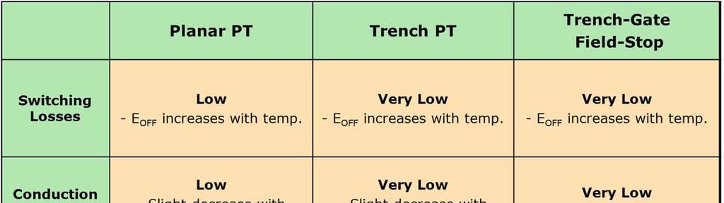
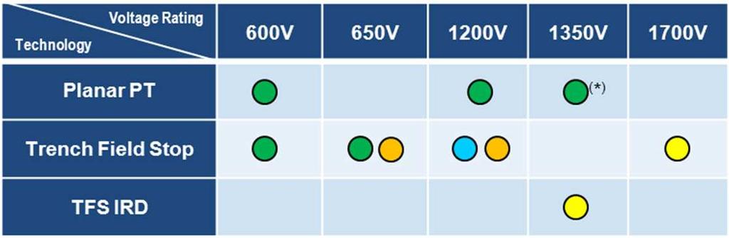

26 IGBT technologies 26
27 IGBT: Nomenclature for New Products 27 STG x 60 H 65 y DD Fy TECHNOLOGY Fx = Trench Gate Field Stop P = Planar PT PACKAGE DIODE FEATURES D = Very Fast Recovery DR = Ultra Fast Recovery DL = Low Forward Voltage B = D 2 PAK D = DPAK E = ISOTOP F = TO-220FP FW = TO-3PF I = I 2 PAK L = PowerFLAT TM (8x8) P = TO-220 U = IPAK (-S for short leads) W = TO-247 WA = TO-247 LL WT = TO-3P Y = Max247 SPECIAL FEATURES BREAKDOWN VOLTAGE 10 TECHNOLOGY SERIES Exception (if any ) C = Current Sensing T = Temperature Sensing Z = Clamped by Zener Diode L = Logic Level H = High speed (8 30 khz) V = Very High speed ( khz) M = Low Loss ( up to 20 khz) MAX CONTINUOUS 100 C

 resulting in a safer")
")
 Low RTH (Thin wafer thickness) Hybrid Electric")
28 Trench Gate Field Stop IGBT: Suitable for high voltage and high current applications Features Low E OFF due to improved minority carrier recombination (Field Stop ) Positive Temperature coefficient in V CE(sat) resulting in a safer paralleling operation Main Applications PhotoVoltaic Uninterruptable Power Supply Welding emitter gate Low V CE(sat) (Trench gate) Power Factor Corrector High switching robusteness (Large SOA) Low RTH (Thin wafer thickness) Hybrid Electric Veichles Induction Heating collector
 Tailored for High speed switching application Preliminary Results (on packaged parts) Symbol Characteristic Typical Value 25 C 150 C BV CES Collector to Emitter breakdown voltage 1200 V")
 I C (nom) P Con (W) P Sw (W) P")
29 1200V IGBT TFS High Frequency series MAT 20 STGW25H120DF Product Features: IGBT in Trench Gate Field Stop Technology 1200V break down rated Final die thickness: 110µm Very low R TH Positive derating of V CE(sat) Tailored for High speed switching application Preliminary Results (on packaged parts) Symbol Characteristic Typical Value 25 C 150 C BV CES Collector to Emitter breakdown voltage 1200 V V CESAT V GE = 15V, I C = 25A V E OFF V CC =600V, V GE =15 0V, R GOFF =22Ω, I C =25A mj Simulated benchmark based on datasheet values Unit Topology: Full Bridge Main Specs: P Out =3kW, f Sw =20kHz, D Max =90%, Î Out 20A, T j =125ºC Device (Trench FS) I C (nom) P Con (W) P Sw (W) P Tot (W) (*) STGW25H120DF 100 C Competitor C Competitor C Competitor C Samples Available (*) switching-on power losses have been neglected for all the devices under benchmark, since they basically depend of co-packaged diode
30 MAT V IGBT TFS High Frequency Final Results (on packaged parts) series STGW60H65DF Product Features: IGBT in Trench Gate Field Stop Technology 650V break down rated Final die thickness: 80µm Very low R TH Positive derating of V CE(sat) Tailored for High speed switching application Symbol BV CES Characteristic Collector to Emitter breakdown voltage Typical Value 25 C 150 C Unit 650 V V CESAT V GE = 15V, I C =60A V E OFF V CC = 400V, V GE = 15V 0, R G = 10Ω, I C = 60A mj Simulated benchmark based on datasheet values Topology: Full Bridge Main Specs: P out =5kW, f sw =16kHz, D Max =90%, Î Out 30A, T J =150ºC Device (Trench FS) I C (nom) P Con (W) P Sw (W) P Tot (W) (*) STGW60H65DF 100 C Competitor C Competitor C Competitor C (*) switching-on power losses have been neglected for all the devices under benchmark, since they basically depend of co-packaged diode

31 600V/650V Discrete IGBT Product Plan H series (8 30 khz) 31 BV CES` I CN 1) V I CN Short Circuit 2) Sales Type Main Applications Packages Eng. Samples Production 600 V 20 A 1.6 V 6 µs STGP20H60DF 30 A 1.9 V 6 µs STGP30H60DF UPS, PFC, motor control UPS, PFC, motor control TO-220, FP Available Production TO-220, FP, TO-247 Available Production 650 V 60 A 1.9 V 6 µs STGW60H65DF Solar, UPS, PFC TO-247 Available Production 60 A 1.9 V 6 µs STGW60H65DRF Solar, UPS, PFC TO-247 Available Production 1) continuous I 100 C 2) Test condition V CC = 400V, V GE = 15V, T Jstart = 25 C T JMAX = 175 C

32
ST High Voltage Power MOSFET
 ST High Voltage Power MOSFET Maurizio Giudice, Marketing Director Power Transistor Division IMS Group March-2012 Market Trend: High efficiency and Emerging Applications 2 Energy efficiency and costs Growing
IGBT and SLLIMM. Technology evolution, Roadmaps and short term new products overview
 IGBT and SLLIMM Technology evolution, Roadmaps and short term new products overview March 2012 IGBT Technology evolution, Roadmaps and short term new products overview 3 IGBTs technologies evolution Trench
HCD80R600R 800V N-Channel Super Junction MOSFET
 HCD80R600R 800V N-Channel Super Junction MOSFET Features Very Low FOM (R DS(on) X Q g ) Extremely low switching loss Excellent stability and uniformity 00% Avalanche Tested Application Switch Mode Power
STB25N80K5, STF25N80K5, STP25N80K5, STW25N80K5
 STB25N80K5, STF25N80K5, STP25N80K5, STW25N80K5 N-channel 800 V, 0.19 Ω typ., 19.5 A MDmesh K5 Power MOSFETs in D 2 PAK, TO-220FP, TO-220 and TO-247 packages Datasheet production data TAB Features TAB 1
STD6N95K5, STP6N95K5 STU6N95K5, STW6N95K5 Datasheet
 STD6N95K5, STP6N95K5 STU6N95K5, STW6N95K5 Datasheet N-channel 950 V, 1 Ω typ., 9 A MDmesh K5 Power MOSFETs in DPAK, TO-220, IPAK and TO-247 packages TAB TAB Features DPAK 1 3 Order codes V DS R DS(on)
STF10N105K5, STP10N105K5, STW10N105K5
 STF10N105K5, STP10N105K5, STW10N105K5 N-channel 1050 V, 1 Ω typ., 6 A MDmesh K5 Power MOSFETs in TO-220, TO-220FP and TO-247 packages Datasheet - production data TAB Features Order codes V DS R DS(on)
Low Voltage Power MOSFET
 Low Voltage Power MOSFET Technical Marketing Power Transistor Division IMS Sector March-2012 Technology Roadmap 10/03/2012 MOSFET Technology Roadmap 4 STripFET V H5 STripFET DeepGATE H6 STripFET DeepGATE
HCS90R1K5R 900V N-Channel Super Junction MOSFET
 HCS90RK5R 900V N-Channel Super Junction MOSFET Features Very Low FOM (R DS(on) X Q g ) Extremely low switching loss Excellent stability and uniformity 00% Avalanche Tested Application Switch Mode Power
N-channel 1050 V, 6 Ω typ., 1.5 A MDmesh K5 Power MOSFETs in DPAK, TO-220 and IPAK packages. Features STU2N105K5. Description.
 STD2N105K5, STP2N105K5, STU2N105K5 N-channel 1050 V, 6 Ω typ., 1.5 A MDmesh K5 Power MOSFETs in DPAK, TO-220 and IPAK packages Datasheet - production data TAB Features DPAK 1 3 Order codes V DS R DS(on)
HCS80R850R 800V N-Channel Super Junction MOSFET
 HCS80R850R 800V N-Channel Super Junction MOSFET Features Very Low FOM (R DS(on) X Q g ) Extremely low switching loss Excellent stability and uniformity 00% Avalanche Tested Application Switch Mode Power
STD4N52K3, STP4N52K3, STU4N52K3
 Datasheet N-channel 525 V, 2.1 Ω typ., 2.5 A MDmesh K3 Power MOSFETs in DPAK, TO-220 and IPAK packages TAB TAB Features DPAK 1 3 TAB TO-220 1 2 3 Order code V DS R DS(on) max. I D Package STD4N52K3 2.5
STD5N95K5, STF5N95K5, STP5N95K5, STU5N95K5
 STD5N95K5, STF5N95K5, STP5N95K5, N-channel 950 V, 2 Ω typ., 3.5 A MDmesh K5 Power MOSFETs in DPAK, TO-220FP, TO-220 and IPAK Datasheet - production data TAB DPAK 2 3 1 TAB 1 2 3 TO-220FP 3 TAB 1 2 1 2
Features. Description. AM01476v1. Table 1. Device summary. Order code Marking Packages Packaging. STF6N95K5 6N95K5 TO-220FP Tube
 N-channel 950 V, 1 Ω typ., 9 A MDmesh K5 Power MOSFET in a TO-220FP package Features Datasheet - production data Order code V DS R DS(on) max. I D P TOT STF6N95K5 950 V 1.25 Ω 9 A 25 W TO-220FP 1 2 3 Figure
STB20N95K5, STF20N95K5, STP20N95K5, STW20N95K5
 STB20N95K5, STF20N95K5, STP20N95K5, N-channel 950 V, 0.275 Ω typ., 17.5 A MDmesh K5 Power MOSFETs in D²PAK, TO-220FP, TO-220 and TO-247 Datasheet packages - production data Features Order code V DS R DS(on)
Automotive-grade N-channel 950 V, Ω typ., 17.5 A MDmesh K5 Power MOSFET in a TO-247 package. Features. Description.
 Automotive-grade N-channel 950 V, 0.280 Ω typ., 17.5 A MDmesh K5 Power MOSFET in a TO-247 package Datasheet - production data Features Order code V DS R DS(on) max. I D P TOT STW22N95K5 950 V 0.330 Ω 17.5
STD2N62K3, STF2N62K3, STU2N62K3
 Datasheet N-channel 620 V, 2.9 Ω typ., 2.2 A MDmesh K3 Power MOSFETs in DPAK, TO-220FP and IPAK packages Features Order code V DS R DS(on) max. I D Package STD2N62K3 STF2N62K3 620 V 3.6 Ω 2.2 A DPAK TO-220FP
Features. Features. Description. Table 1: Device summary Order code Marking Package Packaging STL33N60M2 33N60M2 PowerFLAT 8x8 HV Tape and reel
 N-channel 600 V, 0.115 Ω typ., 22 A MDmesh M2 Power MOSFET in a PowerFLAT 8x8 HV package Datasheet - production data Features Order code V DS @ T Jmax R DS(on)max I D 5 STL33N60M2 650 V 0.135 Ω 22 A 4
HCD80R1K4E 800V N-Channel Super Junction MOSFET
 HCD80R1K4E 800V N-Channel Super Junction MOSFET Features Very Low FOM (R DS(on) X Q g ) Extremely low switching loss Excellent stability and uniformity 100% Avalanche Tested Application Switch Mode Power
Power Semiconductors technologies trends for E-Mobility
 1 Power Semiconductors technologies trends for E-Mobility Gianni Vitale Power Conversion & Drives Section Manager System Lab, STMicroelectronics NESEM 2013, Toulouse All trademarks and logos are property
Features. Table 1: Device summary Order code Marking Package Packing STL10LN80K5 10LN80K5 PowerFLAT 5x6 VHV Tape and reel
 N-channel 800 V, 0.59 Ω typ., 6 A MDmesh K5 Power MOSFET in a PowerFLAT 5x6 VHV package Datasheet - production data Features Order code V DS R DS(on) max. I D STL10LN80K5 800 V 0.66 Ω 6 A 1 2 3 4 PowerFLAT
SSP20N60S / SSF20N60S 600V N-Channel MOSFET
 SSP20N60S / SSF20N60S 600V N-Channel MOSFET Description SJ-FET is new generation of high voltage MOSFET family that is utilizing an advanced charge balance mechanism for outstanding low on-resistance and
I2-PAK I-PAK. TC = 25 C unless otherwise noted D2-PAK/D-PAK I2-PAK / I-PAK/ TO-220
 General Description This Power MOSFET is produced Features using Maple semi s Advanced Super-Junction technology. - 7.6A, 500V, R DS(on) typ. = 0.5Ω@V GS = 10 V This advanced technology has - been Low
HCA60R080FT (Fast Recovery Diode Type) 600V N-Channel Super Junction MOSFET
 600V N-Channel Super Junction MOSFET") HCA60R080FT (Fast Recovery Diode Type) 600V N-Channel Super Junction MOSFET Features Very Low FOM (R DS(on) X Q g ) Extremely low switching loss Excellent stability and uniformity 00% Avalanche Tested
HCA60R080FT (Fast Recovery Diode Type) 600V N-Channel Super Junction MOSFET Features Very Low FOM (R DS(on) X Q g ) Extremely low switching loss Excellent stability and uniformity 00% Avalanche Tested
Symbol Parameter TSB20N60S TSP20N60S TSF20N60S Unit 20* 20* I D -Continuous (TC = 100 ) 12*
 12*") TSP20N60S,TSF20N60S, TSB20N60S 600V N-Channel MOSFET Description SJ-FET is new generation of high voltage MOSFET family that is utilizing an advanced charge balance mechanism for outstanding low on-resistance
TSP20N60S,TSF20N60S, TSB20N60S 600V N-Channel MOSFET Description SJ-FET is new generation of high voltage MOSFET family that is utilizing an advanced charge balance mechanism for outstanding low on-resistance
SUPER-SEMI SUPER-MOSFET. Super Junction Metal Oxide Semiconductor Field Effect Transistor. 800V Super Junction Power Transistor SS*80R380S
 SUPER-SEMI SUPER-MOSFET Super Junction Metal Oxide Semiconductor Field Effect Transistor 800V Super Junction Power Transistor SS*80R380S Rev. 1.2 Oct. 2017 September, 2013 SJ-FET SSF80R380S/SSP80R380S/SSW80R380S/SSA80R380S
SJ-FET TSD5N60S/TSU5N60S
 September, 2013 SJ-FET TSD5N60S/TSU5N60S OSD5N60S/OSU5N60S 600V N-Channel MOSFET Description SJ-FET is new generation of high voltage MOSFET family that is utilizing an advanced charge balance mechanism
HCA80R250T 800V N-Channel Super Junction MOSFET
 HCA80R250T 800V N-Channel Super Junction MOSFET Features Very Low FOM (R DS(on) X Q g ) Extremely low switching loss Excellent stability and uniformity 100% Avalanche Tested Application Switch Mode Power
100% avalanche tested Extremely high dv/dt capability Very low intrinsic capacitance Improved diode reverse recovery characteristics Zener-protected
 Datasheet N-channel 620 V, 1.7 Ω typ., 3.8 A MDmesh K3 Power MOSFET in DPAK package Features TAB Order codes V DS R DS(on) max. I D P TOT 2 3 1 DPAK D(2, TAB) STD4N62K3 620 V 2 Ω 3.8 A 70 W 100% avalanche
Symbol Parameter TSB10N60S TSP10N60S TSF10N60S Unit V DSS Drain-Source Voltage 600 V Drain Current -Continuous (TC = 25 ) 9.5*
 9.5*") TSP10N60S/TSF10N60S /TSB10N60S 600V N-Channel MOSFET Description SJ-FET is new generation of high voltage MOSFET family that is utilizing an advanced charge balance mechanism for outstanding low on-resistance
TSP10N60S/TSF10N60S /TSB10N60S 600V N-Channel MOSFET Description SJ-FET is new generation of high voltage MOSFET family that is utilizing an advanced charge balance mechanism for outstanding low on-resistance
N-channel 600 V, 1.06 Ω typ., 4.5 A MDmesh M2 Power MOSFETs in D 2 PAK and DPAK packages. Features. Description. AM15572v1. Table 1.
 STB6N60M2, STD6N60M2 N-channel 600 V, 1.06 Ω typ., 4.5 A MDmesh M2 Power MOSFETs in D 2 PAK and DPAK packages Features Datasheet - production data Order code V DS @ T Jmax R DS(on) max I D TAB 1 3 2 D
Features. Description. Table 1: Device summary Order code Marking Package Packing STP5N80K5 5N80K5 TO-220 Tube
 N-channel 800 V, 1.50 Ω typ., 4 A MDmesh K5 Power MOSFET in a TO-220 package Datasheet - production data Features Order code VDS RDS(on) max. ID STP5N80K5 800 V 1.75 Ω 4 A Industry s lowest RDS(on) x area
Features. Description. Table 1: Device summary. Order code Marking Package Packing STL24N60DM2 24N60DM2 PowerFLAT 8x8 HV Tape and reel
 N-channel 600 V, 0.195 Ω typ., 15 A MDmesh DM2 Power MOSFET in a PowerFLAT 8x8 HV package Datasheet - production data Features Order code VDS @ TJmax RDS(on) max. ID 5 STL24N60DM2 650 V 0.220 Ω 15 A 4
Schematic diagram R DS(ON) < V GS =10V. Marking and pin assignment Uninterruptible power supply
 < V GS =10V. Marking and pin assignment Uninterruptible power supply") FNK N-Channel Enhancement Mode Power MOSFET Description The FNK 85H21 uses advanced trench technology and design to provide excellent R DS(ON) with low gate charge. It can be used in automotive applications
FNK N-Channel Enhancement Mode Power MOSFET Description The FNK 85H21 uses advanced trench technology and design to provide excellent R DS(ON) with low gate charge. It can be used in automotive applications
STGW25H120DF2, STGWA25H120DF2
 STGW25H120DF2, STGWA25H120DF2 Trench gate field-stop IGBT, H series 1200 V, 25 A high speed Features Datasheet - production data Maximum junction temperature: T J = 175 C High speed switching series Minimized
PWRLITE LU1014D High Performance N-Channel POWERJFET TM with PN Diode
 PWRLITE LU114D High Performance N-Channel POWERJFET TM with PN Diode Features Superior gate charge x Rdson product (FOM) Trench Power JFET with low threshold voltage Vth. Device fully ON with Vgs =.7V
STF12N120K5, STFW12N120K5
 STF12N120K5, STFW12N120K5 N-channel 1200 V, 0.62 Ω typ., 12 A MDmesh K5 Power MOSFETs in TO-220FP and TO-3PF packages Features Datasheet - production data Order code V DS R DS(on) max. I D P TOT TO-220FP
HCD80R650E 800V N-Channel Super Junction MOSFET
 HCD80R650E 800V N-Channel Super Junction MOSFET Features Very Low FOM (R DS(on) X Q g ) Extremely low switching loss Excellent stability and uniformity 100% Avalanche Tested Application Switch Mode Power
SJ-FET. TSA20N60S, TSK20N60S 600V N-Channel MOSFET. September, 2013
 TSA20N60S, TSK20N60S 600V N-Channel MOSFET Description SJ-FET is new generation of high voltage MOSFET family that is utilizing an advanced charge balance mechanism for outstanding low on-resistance and
STP5N105K5. N-channel 1050 V, 2.9 Ω typ., 3 A MDmesh K5 Power MOSFET in a TO-220 package. Features. Applications. Description
 STP5N05K5 N-channel 050 V, 2.9 Ω typ., 3 A MDmesh K5 Power MOSFET in a TO-220 package Datasheet - production data Features Order code VDS RDS(on) max. ID PTOT STP5N05K5 050 V 3.5 Ω 3 A 85 W Worldwide best
Features. Description. Table 1: Device summary Order code Marking Package Packing STL10N65M2 10N65M2 PowerFLAT 5x6 HV Tape and reel
 N-channel 650 V, 0.85 Ω typ., 4.5 A MDmesh M2 Power MOSFET in a PowerFLAT 5x6 HV package Datasheet - production data Features Order code VDS RDS(on) max. ID STL10N65M2 650 V 1.00 Ω 4.5 A 1 2 3 4 PowerFLAT
STD7N60M2, STP7N60M2, STU7N60M2
 Datasheet N-channel 600 V, 0.86 Ω typ., 5 A, MDmesh M2 Power MOSFETs in DPAK, TO-220 and IPAK packages TAB TAB Features DPAK 1 3 TAB TO-220 1 2 3 Order codes V DS @ T Jmax R DS(on) max. I D STD7N60M2 STP7N60M2
STB100N10F7, STD100N10F7, STF100N10F7 STI100N10F7, STP100N10F7 Datasheet
 STB100N10F7, STD100N10F7, STF100N10F7 STI100N10F7, STP100N10F7 Datasheet N-channel 100 V, 6.8 mω typ., 80 A STripFET F7 Power MOSFETs in D 2 PAK, DPAK, TO-220FP, I 2 PAK and TO-220 packages TAB TAB Features
Features. Description. Table 1: Device summary Order code Marking Package Packing STW12N150K5 12N150K5 TO-247 Tube
 N-channel 1500 V, 1.6 Ω typ.,7 A MDmesh K5 Power MOSFET in a TO-247 package Datasheet - production data Features Order code V DS R DS(on) max. I D P TOT STW12N150K5 1500 V 1.9 Ω 7 A 250 W 1 3 2 Industry
N-channel 30 V, Ω typ., 23 A STripFET H7 Power MOSFET plus monolithic Schottky in a PowerFLAT 3.3 x 3.3. Features.
 N-channel 30 V, 0.0027 Ω typ., 23 A STripFET H7 Power MOSFET plus monolithic Schottky in a PowerFLAT 3.3 x 3.3 Datasheet - production data Features Order code V DS R DS(on) max I D STL23NS3LLH7 30 V 0.0037
STP3LN80K5, STU3LN80K5
 N-channel 800 V, 2.75 Ω typ., 2 A MDmesh K5 Power MOSFET in TO-220 and IPAK packages Datasheet - production data TAB Features Order code V DS RDS(on) max ID TAB IPAK 3 2 1 TO-220 1 2 3 STP3LN80K5 800 V
HCS80R1K4E 800V N-Channel Super Junction MOSFET
 HCS80R1K4E 800V N-Channel Super Junction MOSFET Features Very Low FOM (R DS(on) X Q g ) Extremely low switching loss Excellent stability and uniformity 100% Avalanche Tested Application Switch Mode Power
SiC Cascodes and its advantages in power electronic applications
 SiC Cascodes and its advantages in power electronic applications WBG Power Conference, Munich, 5 th December 2017 Christopher Rocneanu Director Sales Europe and North America cro@unitedsic.com +4915121063411
Prerelease Product(s) - Prerelease Product(s)
 - Prerelease Product(s)") N-channel 1500 V, 1.6 Ω typ.,7 A MDmesh K5 Power MOSFET in a TO-220FP wide creepage package Figure 1: Internal schematic diagram Features Order code VDS Datasheet - preliminary data RDS(on) max. ID PTOT
N-channel 1500 V, 1.6 Ω typ.,7 A MDmesh K5 Power MOSFET in a TO-220FP wide creepage package Figure 1: Internal schematic diagram Features Order code VDS Datasheet - preliminary data RDS(on) max. ID PTOT
STH12N120K5-2, STP12N120K5, STW12N120K5, STWA12N120K5
 STH12N120K5-2, STP12N120K5, N-channel 1200 V, 0.62 Ω typ.,12 A MDmesh K5 Power MOSFETs in H²PAK-2, TO-220, TO-247 and TO-247 long leads Datasheet - production data Features Order codes V DS R DS(on) max.
Features. Description. AM15572v1_no_tab. Table 1: Device summary Order code Marking Package Packing STF7LN80K5 7LN80K5 TO-220FP Tube
 N-channel 800 V, 0.95 Ω typ., 5 A MDmesh K5 Power MOSFET in a TO-220FP package Datasheet - production data Features Order code V DS R DS(on) max. I D STF7LN80K5 800 V 1.15 Ω 5 A 3 1 2 TO-220FP Figure 1:
Device Marking Device Device Package Reel Size Tape width Quantity TO-252-2L. Parameter Symbol Limit Unit
 HM80N05K N-Channel Enhancement Mode Power MOSFET Description The uses advanced trench technology and design to provide excellent R DS(ON) with low gate charge. It can be used in a wide variety of applications.
STF14N80K5, STFI14N80K5
 STF14N80K5, STFI14N80K5 N-channel 800 V, 0.400 Ω typ., 12 A MDmesh K5 Power MOSFETs in TO-220FP and I²PAKFP packages Datasheet - production data Features Order code V DS R DS(on) max. I D STF14N80K5 STFI14N80K5
PKP3105. P-Ch 30V Fast Switching MOSFETs
 Super Low Gate Charge % EAS Guaranteed Green Device Available Excellent CdV/dt effect decline Advanced high cell density Trench technology Product Summary BVDSS RDSON ID -3V mω -6A Description TO22 Pin
Features. Description. AM01476v1. Table 1. Device summary. Order codes Marking Package Packaging. STW70N60M2 70N60M2 TO-247 Tube
 N-channel 600 V, 0.03 Ω typ., 68 A MDmesh M2 Power MOSFET in a TO-247 package Features Datasheet production data Order codes V DS @ T Jmax R DS(on) max I D STW70N60M2 650 V 0.040 Ω 68 A TO-247 1 2 3 Extremely
IGBT Technologies and Applications Overview: How and When to Use an IGBT Vittorio Crisafulli, Apps Eng Manager. Public Information
 IGBT Technologies and Applications Overview: How and When to Use an IGBT Vittorio Crisafulli, Apps Eng Manager Agenda Introduction Semiconductor Technology Overview Applications Overview: Welding Induction
HCS80R380R 800V N-Channel Super Junction MOSFET
 HCS8R38R 8V N-Channel Super Junction MOSFET Features Very Low FOM (R DS(on) X Q g ) Extremely low switching loss Excellent stability and uniformity % Avalanche Tested Application Switch Mode Power Supply
Features. Description. AM15572v1_no_tab. Table 1: Device summary Order code Marking Package Packing STF4N90K5 4N90K5 TO-220FP Tube
 N-channel 900 V, 1.90 Ω typ., 4 A MDmesh K5 Power MOSFET in a TO-220FP package Datasheet - production data Features Order code VDS RDS(on) max. ID STF4N90K5 900 V 2.10 Ω 4 A TO-220FP Figure 1: Internal
Order code V DS R DS(on) max. I D
 max. I D") Datasheet N-channel 6 V, 61 mω typ., 39 A, MDmesh M6 Power MOSFET in a TO 247 package Features Order code V DS R DS(on) max. I D STW48N6M6 6 V 69 mω 39 A TO-247 D(2, TAB) 1 3 2 Reduced switching losses
Datasheet N-channel 6 V, 61 mω typ., 39 A, MDmesh M6 Power MOSFET in a TO 247 package Features Order code V DS R DS(on) max. I D STW48N6M6 6 V 69 mω 39 A TO-247 D(2, TAB) 1 3 2 Reduced switching losses
Order code V DS R DS(on ) max. I D
 max. I D") Datasheet N-channel 9 V,.21 Ω typ., 2 A MDmesh K5 Power MOSFET in a TO 22FP package Features TO-22FP D(2) 1 2 3 Order code V DS R DS(on ) max. I D STF2N9K5 9 V.25 Ω 2 A Industry s lowest R DS(on) x area
Datasheet N-channel 9 V,.21 Ω typ., 2 A MDmesh K5 Power MOSFET in a TO 22FP package Features TO-22FP D(2) 1 2 3 Order code V DS R DS(on ) max. I D STF2N9K5 9 V.25 Ω 2 A Industry s lowest R DS(on) x area
N-channel 650 V, 1.6 Ω typ., 2.3 A MDmesh M2 Power MOSFET in a PowerFLAT 3.3x3.3 HV package. Features
 N-channel 650 V, 1.6 Ω typ., 2.3 A MDmesh M2 Power MOSFET in a PowerFLAT 3.3x3.3 HV package Datasheet - production data Features 1 2 3 4 Order code VDS RDS(on) max. ID STL3N65M2 650 V 1.8 Ω 2.3 A 8 7 6
AUTOMOTIVE MOSFET. HEXFET Power MOSFET Wiper Control
 AUTOMOTIVE MOSFET PD -94A IRFBA405P Typical Applications Electric Power Steering (EPS) Anti-lock Braking System (ABS) HEXFET Power MOSFET Wiper Control D Climate Control V DSS = 55V Power Door Benefits
STB22NM60N, STF22NM60N, STP22NM60N
 Datasheet N-channel 600 V, 0.20 Ω typ., 16 A MDmesh II Power MOSFETs in D²PAK, TO-220FP and TO-220 packages TAB Features 3 1 2 D PAK TAB 1 2 3 TO-220FP Order code STB22NM60N V DS @ T jmax. R DS(on) max.
PFP15T140 / PFB15T140
 FEATURES 1% EAS Test Super high density cell design Extremely Low Intrinsic Capacitances Remarkable Switching Characteristics Extended Safe Operating Area Lower R DS(ON) : 6. mω (Typ.) @ =1V 15V N-Channel
Features. Description. Table 1: Device summary Order code Marking Package Packing STB20N90K5 20N90K5 D²PAK Tape and reel
 N-channel 900 V, 0.21 Ω typ., 20 A MDmesh K5 Power MOSFET in a D²PAK package Datasheet - production data Features TAB Order code VDS RDS(on) max. ID STB20N90K5 900 V 0.25 Ω 20 A 2 3 1 D²PAK Industry s
HCI70R500E 700V N-Channel Super Junction MOSFET
 HCI70R500E 700V N-Channel Super Junction MOSFET Features Very Low FOM (R DS(on) X Q g ) Extremely low switching loss Excellent stability and uniformity 100% Avalanche Tested Higher dv/dt ruggedness Application
Features. Description. Table 1: Device summary. Order code Marking Package Packing STW75N60M6 75N60M6 TO-247 Tube
 N-channel 600 V, 32 mω typ., 72 A MDmesh M6 Power MOSFET in TO-247 package Datasheet - production data Features Order code VDS RDS(on) max. ID STW75N60M6 600 V 36 mω 72 A 3 2 1 TO-247 Figure 1: Internal
Features. Description. Table 1: Device summary Order code Marking Package Packing STF23N80K5 23N80K5 TO-220FP Tube
 N-channel 800 V, 0.23 Ω typ., 16 A MDmesh K5 Power MOSFET in a TO-220FP package Datasheet - production data Features Order code VDS RDS(on) max. ID PTOT STF23N80K5 800 V 0.28 Ω 16 A 35 W TO-220FP Figure
TO-220. Item Sales Type Marking Package Packaging 1 SW P 640 SW640 TO-220 TUBE 2 SW W 640 SW640 TO-3P TUBE
 N-channel MOSFET Features High ruggedness R DS(ON) (Max 0.8 Ω)@V GS =0V Gate Charge (Typical 35nC) Improved dv/dt Capability 00% Avalanche Tested 2 3 2 3. Gate 2. Drain 3. Source General Description This
STD5N60M2, STP5N60M2, STU5N60M2
 Datasheet N-channel 600 V, 1.3 Ω typ., 3.5 A, MDmesh M2 Power MOSFETs in DPAK, TO-220 and IPAK packages TAB TAB Features DPAK 1 3 TAB TO-220 1 2 3 Order code V DS @ T Jmax R DS(on) max. I D STD5N60M2 STP5N60M2
Features. Description. AM15572v1_no_tab. Table 1: Device summary Order code Marking Package Packing STF10LN80K5 10LN80K5 TO-220FP Tube
 N-channel 800 V, 0.55 Ω typ., 8 A MDmesh K5 Power MOSFET in a TO-220FP package Datasheet - production data Features Order code V DS R DS(on) max. I D STF10LN80K5 800 V 0.63 Ω 8 A TO-220FP Figure 1: Internal
Features. Description. AM15572v1_no_tab. Table 1: Device summary Order code Marking Package Packing STFH18N60M2 18N60M2 TO-220FP wide creepage Tube
 N-channel 600 V, 0.255 Ω typ., 13 A MDmesh M2 Power MOSFET in a TO-220FP wide creepage package Datasheet - production data Features Order code VDS @ TJmax RDS(on) max ID STFH18N60M2 650 V 0.28 Ω 13 A Extremely
STD2N80K5, STF2N80K5, STP2N80K5, STU2N80K5
 STD2N80K5, STF2N80K5, STP2N80K5, STU2N80K5 N-channel 800 V, 3.5 Ω typ., 2 A Zener-protected SuperMESH 5 Power MOSFET in DPAK, TO-220FP, TO-220 and IPAK packages Datasheet production data TAB Features TAB
Automotive-grade N-channel 60 V, 1.2 mω typ., 120 A STripFET F7 Power MOSFET in a PowerFLAT 5x6 package. Features. Description
 Automotive-grade N-channel 60 V, 1.2 mω typ., 120 A STripFET F7 Power MOSFET in a PowerFLAT 5x6 package Datasheet - production data Features Order code V DS RDS(on) max ID STL225N6F7AG 60 V 1.4 mω 120
STD16N50M2, STF16N50M2, STP16N50M2
 Datasheet N-channel 500 V, 0.24 Ω typ., 13 A MDmesh M2 Power MOSFETs in DPAK, TO-220FP and TO-220 packages TAB 3 2 1 DPAK Features Order code V DS at T J max. R DS(on) max. I D Packages TAB STD16N50M2
Switch mode power supplies Low gate charge. Power factor correction modules Low intrinsic capacitance
 Description United Silicon Carbide's cascode products co-package its highperformance F3 SiC fast JFETs with a cascode optimized MOSFET to produce the only standard gate drive SiC device in the market today.
Power Matters Microsemi SiC Products
 Microsemi SiC Products James Kerr Director of Marketing Power Discrete Products Microsemi Power Products MOSFETs (100V-1200V) Highest Performance SiC MOSFETs 1200V MOSFETs FREDFETs (MOSFET with fast body
35mW V SiC Cascode UJ3C120040K3S Datasheet. Description. Typical Applications. Maximum Ratings
 Description United Silicon Carbide's cascode products co-package its highperformance G3 SiC JFETs with a cascode optimized MOSFET to produce the only standard gate drive SiC device in the market today.
SMPS MOSFET. V DSS Rds(on) max I D
 max I D") Applications Switch Mode Power Supply ( SMPS ) Uninterruptable Power Supply High speed power switching Lead-Free Benefits Low Gate Charge Qg results in Simple Drive Requirement Improved Gate, Avalanche
Applications Switch Mode Power Supply ( SMPS ) Uninterruptable Power Supply High speed power switching Lead-Free Benefits Low Gate Charge Qg results in Simple Drive Requirement Improved Gate, Avalanche
Features. Description. AM01476v1. Table 1. Device summary. Order code Marking Package Packaging. STF10N80K5 10N80K5 TO-220FP Tube
 N-channel 800 V, 0.470 Ω typ., 9 A MDmesh K5 Power MOSFET in a TO-220FP package Features Datasheet - production data Order code V DS R DS(on) max I D P TOT STF10N80K5 800 V 0.600 Ω 9 A 30 W TO-220FP Figure
STD10P6F6, STF10P6F6, STP10P6F6, STU10P6F6
 STD10P6F6, STF10P6F6, STP10P6F6, STU10P6F6 P-channel -60 V, 0.13 Ω typ., -10 A STripFET F6 Power MOSFETs in DPAK, TO-220FP, TO-220 and IPAK packages Features Datasheet production data TAB Order codes V
Features. Description. AM15572v1. Table 1. Device summary. Order code Marking Package Packaging. STD7N65M2 7N65M2 DPAK Tape and reel
 N-channel 650 V, 0.98 Ω typ., 5 A MDmesh M2 Power MOSFET in a DPAK package Features Datasheet - production data TAB Order code V DS R DS(on) max STD7N65M2 650 V 1.15 Ω 5 A I D DPAK 1 3 Extremely low gate
Switch mode power supplies Low gate charge. Power factor correction modules Low intrinsic capacitance
 Description United Silicon Carbide's cascode products co-package its highperformance F3 SiC fast JFETs with a cascode optimized MOSFET to produce the only standard gate drive SiC device in the market today.
STD1NK60 - STD1NK60-1 STQ1HNK60R - STN1HNK60 N-CHANNEL 600V - 8Ω - 1A DPAK/TO-92/IPAK/SOT-223 SuperMESH MOSFET
 STD1NK60 - STD1NK60-1 STQ1HNK60R - STN1HNK60 N-CHANNEL 600V - 8Ω - 1A DPAK/TO-92/IPAK/SOT-223 SuperMESH MOSFET Table 1: General Features TYPE V DSS R DS(on) I D Pw STD1NK60 STD1NK60-1 STQ1HNK60R STN1HNK60
SUPER-SEMI SUPER-MOSFET. Super Junction Metal Oxide Semiconductor Field Effect Transistor. 600V Super Junction Power Transistor SS*20N60S. Rev. 1.
 SUPER-SEMI SUPER-MOSFET Super Junction Metal Oxide Semiconductor Field Effect Transistor 600V Super Junction Power Transistor SS*20N60S Rev. 1.04 September, 2013 SSW20N60S/SSA20N60S 600V N-Channel MOSFET
STD12N65M2. N-channel 650 V, 0.42 Ω typ., 8 A MDmesh M2 Power MOSFET in a DPAK package. Features. Applications. Description DPAK (TO-252)
") N-channel 650 V, 0.42 Ω typ., 8 A MDmesh M2 Power MOSFET in a DPAK package Datasheet - production data Features Order code V DS R DS(on)max. I D 650 V 0.5 Ω 8 A DPAK (TO-252) Extremely low gate charge
N-channel 650 V, 0.42 Ω typ., 8 A MDmesh M2 Power MOSFET in a DPAK package Datasheet - production data Features Order code V DS R DS(on)max. I D 650 V 0.5 Ω 8 A DPAK (TO-252) Extremely low gate charge
Among the lowest R DS(on) on the market Excellent FoM (figure of merit) Low C rss /C iss ratio for EMI immunity High avalanche ruggedness
 on the market Excellent FoM (figure of merit) Low C rss /C iss ratio for EMI immunity High avalanche ruggedness") N-channel 100 V, 5 mω typ., 107 A, STripFET F7 Power MOSFET in a PowerFLAT 5x6 package Features Order code V DS R DS(on) max. I D P TOT STL110N10F7 100 V 6 mω 107 A 136 W Among the lowest R DS(on) on the
N-channel 100 V, 5 mω typ., 107 A, STripFET F7 Power MOSFET in a PowerFLAT 5x6 package Features Order code V DS R DS(on) max. I D P TOT STL110N10F7 100 V 6 mω 107 A 136 W Among the lowest R DS(on) on the
PFU70R360G / PFD70R360G
 FEATURES New technology for high voltage device Low RDS(on) low conduction losses Small package Ultra low gate charge cause lower driving requirement 100% avalanche tested Halogen Free APPLICATION Power
Features. Order code. Description. Table 1: Device summary Order code Marking Package Packing STL28N60DM2 28N60DM2 PowerFLAT 8x8 HV Tape and reel
 N-channel 600 V, 0.155 Ω typ., 21 A MDmesh DM2 Power MOSFET in a PowerFLAT 8x8 HV package Datasheet - production data Features 4 5 3 2 1 PowerFLAT 8x8 HV Figure 1: Internal schematic diagram Order code
HCS70R1K6 700V N-Channel Super Junction MOSFET
 HCS70RK6 700 NChannel Super Junction MOSFET Features ery Low FOM (R DS(on) X Qg) Extremely low switching loss Excellent stability and uniformity 00% valanche Tested Builtin ESD Diode pplication Switch
Features. Symbol Parameter Rating Units V DS Drain-Source Voltage 60 V V GS Gate-Source Voltage ±20 V
 General Description These N-Channel enhancement mode power field effect transistors are using trench DMOS technology. This advanced technology has been especially tailored to minimize on-state resistance,
Device Marking Device Device Package Reel Size Tape width Quantity SIP3210 SIP3210 SOP-8 330mm
 SIAI N-Channel Enhancement Mode Power MOSFET DESCRIPTION The SIP3210 uses advanced trench technology and design to provide excellent R DS(ON) with low gate charge. It can be used in a wide variety of applications.
SUPER-SEMI SUPER-MOSFET. Super Junction Metal Oxide Semiconductor Field Effect Transistor. 800V Super Junction Power Transistor SS*80R240S
 SUPER-SEMI SUPER-MOSFET Super Junction Metal Oxide Semiconductor Field Effect Transistor 800V Super Junction Power Transistor SS*80R240S Rev. 1.1 Aug. 2017 SSP80R240S/SSF80R240S/SSB80R240S 800V N-Channel
Features. Description. AM15572v1_tab. Table 1: Device summary Order code Marking Package Packing STD7LN80K5 7LN80K5 DPAK Tape and reel
 N-channel 800 V, 0.95 Ω typ., 5 A MDmesh K5 Power MOSFET in a DPAK package Datasheet - production data Features Order code V DS R DS(on) max. I D STD7LN80K5 800 V 1.15 Ω 5 A DPAK Figure 1: Internal schematic
STB18N60M2, STI18N60M2 STP18N60M2, STW18N60M2 Datasheet
 STB18N60M2, STI18N60M2 STP18N60M2, STW18N60M2 Datasheet N-channel 600 V, 0.255 Ω typ., 13 A MDmesh M2 Power MOSFETs in D 2 PAK, I 2 PAK, TO-220 and TO-247 packages TAB TAB Features Order codes V DS @ T
SMD Type. P-Channel Enhancement MOSFET IRLML6401 (KRLML6401) Features. Absolute Maximum Ratings Ta = 25
 Features. Absolute Maximum Ratings Ta = 25") SMD Type P-Channel Enhancement IRLML640 (KRLML640) Features Ultra low on-resistance. P-Channel. Fast switching. 2.4 - + SOT-23 3 2.9 - + 0.4 - + 2.3 - + 0.55 0.4 Unit: mm 0.95 - +.9 - + -0.0 +0.05 0-0.38
SMD Type P-Channel Enhancement IRLML640 (KRLML640) Features Ultra low on-resistance. P-Channel. Fast switching. 2.4 - + SOT-23 3 2.9 - + 0.4 - + 2.3 - + 0.55 0.4 Unit: mm 0.95 - +.9 - + -0.0 +0.05 0-0.38
SGT160N60W3/SGF160N60W3/SGW160N60W3
 600V, 22A, 0.160Ω Features RDS(on) = 0.160Ω (Max.)@ VGS = 10V, ID = 11A Ultra low gate charge ( Typ. Qg = 45nC) Low effective output capacitance 100% avalanche tested RoHS compliant Description The WinMOS
STO36N60M6. N-channel 600 V, 85 mω typ., 30 A, MDmesh M6 Power MOSFET in a TO LL HV package. Datasheet. Features. Applications.
 Datasheet N-channel 600 V, 85 mω typ., 30 A, MDmesh M6 Power MOSFET in a TO LL HV package Features Order code V DS R DS(on) max. I D 600 V 99 mω 30 A Drain (TAB) Reduced switching losses Lower R DS(on)
STGW15H120DF2, STGWA15H120DF2
 STGW15H120DF2, STGWA15H120DF2 Trench gate field-stop IGBT, H series 1200 V, 15 A high speed Features Datasheet - production data Maximum junction temperature: T J = 175 C High speed switching series Minimized
TO-220F. 1. Gate 2. Drain 3. Source. Item Sales Type Marking Package Packaging 1 SW P 4N60 SW4N60 TO-220 TUBE 2 SW F 4N60 SW4N60 TO-220F TUBE
 N-channel MOSFET Features High ruggedness R DS(ON) (Max 2.2 Ω)@V GS =0V Gate Charge (Typ 30nC) Improved dv/dt Capability 00% Avalanche Tested 2 3 TO-220F 2 3 TO-220 BS : 600V I D : 4.0A R DS(ON) : 2.2ohm
Features. Description. Table 1: Device summary Order code Marking Package Packing STF24N60DM2 24N60DM2 TO-220FP Tube
 N-channel 600 V, 0.175 Ω typ., 18 A MDmesh DM2 Power MOSFET in a TO-220FP package Datasheet - production data Features Order code VDS @ TJmax RDS(on) max. ID 650 V 0.200 Ω 18 A TO-220FP Fast-recovery body