Glass Processing. Younès Messaddeq Centre d optique, Photonique et laser,québec, Canada Spring 2015 JIRU
|
|
|
- Colin Boyd
- 5 years ago
- Views:
Transcription
1 Glass Processing Lecture 19 # Introduction to Dielectric Waveguide Younès Messaddeq Centre d optique, Photonique et laser,québec, Canada (younes.messaddeq@copl.ulaval.ca) Spring 2015 Lectures available at: Sponsored by US National Science Foundation (DMR )
2 Introduction to Dielectric Waveguide OUTLINE Day One (Introduction to Dielectric Waveguide) 1 Introduction & Useful references 2 Dielectric waveguide Representative of Chanel waveguides Waveguide condition Single and multimode waveguide TE and TM modes 3- Waveguides Materials 4-Characterization of Optical Waveguides 5- Waveguide devices
 Hardcover October 25, 2012 by Safa O. Kasap (Author) ISBN-10: 0133081753 Second Edition Version 1.056")
3 Introduction to Dielectric Waveguide USEFUL REFERENCE Optoelectronics & Photonics: Principles & Practices (2nd Edition) Hardcover October 25, 2012 by Safa O. Kasap (Author) ISBN-10: Second Edition Version 1.056
4 Introduction to Dielectric Waveguide USEFUL REFERENCE Optical Waveguides (OPT568) Govind P. Agrawal Institute of Optics University of Rochester Rochester, NY Photonics devices Jia-Ming Liu Electrical Engineering Department University of California Los Angeles, CA
5 Introduction The basic element of any optical circuit is the optical waveguide which permits to connect optically different devices. To build integrated optical circuits that substitute micro-electronic circuits, integrated optical waveguides with light confinement in a size of the order of the wavelength are mandatory. Optical waveguides can be classified according to their : a) Geometry: Planar, Strip, Fiber waveguides b) Mode Structure: Single mode, multimode c) Rectractive index distribution: Step, Gradient index d) Material: Glass, Polymer, Semicomducteur.
6 Introduction
7 Introduction Optical integrated waveguides: -Design: energy flow only along the waveguiding structure but not perpendicular to it, so radiation losses can be avoided -Mechanism: usually, optical integrated waveguides rely on the principle of total internal reflection (TIR) -Material science: use of materials with good optical properties: low absorption loss is fundamental. -Integration: The waveguide cross-section should be as small as possible to permit high-density integration (physical limit: diffraction, size λ/2) -Functionality: linking devices or systems (i.e., optical fiber) or implementation of complex functionalities: splitters/combiners, couplers, AWGs, modulators, etc. -Technology: Importance of the employed materials and related-technology: Silicon/silica, SiN, polymers, III-V compounds, lithium niobate, etc.
8 DIELECTRIC WAVEGUIDES

9 Representative of Chanel Waveguides


10 Representative of Chanel Waveguides A buried channel waveguide is formed with a high-index waveguiding core buried in a lowindex surrounding medium. A ridge waveguide has a structure that looks like a strip waveguide, but the strip, or the ridge, on top of its planar structure has a high index and is actually the waveguiding core. A ridge waveguide has strong optical confinement because it is surrounded on three sides by low-index air (or cladding material). A rib waveguide has a structure similar to that of a strip or ridge waveguide, but the strip has the same index as the high index planar layer beneath it and is part of the waveguiding core.

11 Representative of Chanel Waveguides A strip-loaded waveguide is formed by loading a planar waveguide, which already provides optical confinement in the x direction, with a dielectric strip of index n3<n1 or a metal strip to facilitate optical confinement in the y direction. The waveguiding core of a strip waveguide is the n1 region under the loading strip, with its thickness d determined by the thickness of the n1 layer and its width w defined by the width of the loading strip. A diffused waveguide is formed by creating a highindex region in a substrate through diffusion of dopants, such as LiNbO 3 waveguide with a core formed by Ti diffusion.

12 Planar Optical Waveguide A planar dielectric waveguide has a central rectangular region of higher refractive index n 1 than the surrounding region which has a refractive index n 2. It is assumed that the waveguide is infinitely wide and the central region is of thickness 2a. It is illuminated at one end by a nearly monochromatic light source. Optoelectronics & Photonics: Principles & Practices (2nd Edition) Hardcover October 25, 2012 by Safa O. Kasap (Author)
13 Waves Inside the Core A light ray traveling in the guide must interfere constructively with itself to propagate successfully. Otherwise destructive interference will destroy the wave. E is parallel to x. (l 1 and k 1 are the wavelength and the propagation constant inside the core medium n 1 i.e. l 1 = l/n 1.) Optoelectronics & Photonics: Principles & Practices (2nd Edition) Hardcover October 25, 2012 by Safa O. Kasap (Author)
![Waveguide Condition And Modes k 1 = kn 1 = 2pn 1 /l, Df(AC) = k 1 (AB + BC) - 2f = m(2p) BC = d/cosq and AB = BCcos(2q) AB + BC = BCcos(2q) + BC = BC[(2cos 2 q -1) + 1] = 2dcosq k 1 [2dcosq] - 2f =](/docs-images/81/82953201/images/14-1.jpg "m(2p) 2pn 1 (2a) l cosq m Waveguide condition -f m mp m = 0, 1, 2, 3 etc Integer Mode number Optoelectronics & Photonics: Principles & Practices (2nd Edition) Hardcover October 25, 2012 by Safa O.")
14 Waveguide Condition And Modes k 1 = kn 1 = 2pn 1 /l, Df(AC) = k 1 (AB + BC) - 2f = m(2p) BC = d/cosq and AB = BCcos(2q) AB + BC = BCcos(2q) + BC = BC[(2cos 2 q -1) + 1] = 2dcosq k 1 [2dcosq] - 2f = m(2p) 2pn 1 (2a) l cosq m Waveguide condition -f m mp m = 0, 1, 2, 3 etc Integer Mode number Optoelectronics & Photonics: Principles & Practices (2nd Edition) Hardcover October 25, 2012 by Safa O. Kasap (Author)

15 Waves Inside the Core Two arbitrary waves 1 and 2 that are initially in phase must remain in phase after reflections. Otherwise the two will interfere destructively and cancel each other. Optoelectronics & Photonics: Principles & Practices (2nd Edition) Hardcover October 25, 2012 by Safa O. Kasap (Author)
16 Waveguide Condition And Modes m m k k 2pn 1 1 sinq m l 2pn l 1 1 cosq m sinq cosq m m Propagation constant along the guide Transverse Propagation constant Optoelectronics & Photonics: Principles & Practices (2nd Edition) Hardcover October 25, 2012 by Safa O. Kasap (Author)

17 Modes in a Planar Waveguide We can identify upward (A) and downward (B) traveling waves in the guide which interfere to set up a standing wave along y and a wave that is propagating along z. Rays 2 and 2 belong to the same wave front but 2 becomes reflected before 2. The interference of 1 and 2 determines the field at a height y from the guide center. The field E(y, z, t) at P can be written as: E(y,z,t) = E m (y)cos(wt - m z) Traveling wave along z Field pattern along y Optoelectronics & Photonics: Principles & Practices (2nd Edition) Hardcover October 25, 2012 by Safa O. Kasap (Author)

18 Mode Field Pattern Left: The upward and downward traveling waves have equal but opposite wavevectors m and interfere to set up a standing electric field pattern across the guide. Right: The electric field pattern of the lowest mode traveling wave along the guide. This mode has m = 0 and the lowest q. It is often referred to as the glazing incidence ray. It has the highest phase velocity along the guide Optoelectronics & Photonics: Principles & Practices (2nd Edition) Hardcover October 25, 2012 by Safa O. Kasap (Author)

19 Modes in a Planar Waveguide The electric field patterns of the first three modes (m = 0, 1, 2) traveling wave along the guide. Notice different extents of field penetration into the cladding. Each of these traveling wave constitutes a mode of propagation. Optoelectronics & Photonics: Principles & Practices (2nd Edition) Hardcover October 25, 2012 by Safa O. Kasap (Author)
 l cosq m -f m mp Optoelectronics & Photonics: Principles & Practices (2nd Edition) Hardcover October 25, 2012 by Safa O.")
20 Waveguide Condition and Modes To get a propagating wave along a guide you must have constructive interference. All these rays interfere with each other. Only certain angles are allowed. Each allowed angle represents a mode of propagation. 2pn 1 (2a) l cosq m -f m mp Optoelectronics & Photonics: Principles & Practices (2nd Edition) Hardcover October 25, 2012 by Safa O. Kasap (Author)
21 TE and TM Modes Two of the possibilities for the electric field direction of a wave Traveling toward the core-cladding boundary. B^ is along - x, so that B^ = -B x E^ is along x, so that E^ = E x Possible modes can be classified in terms of : (a) transverse electric field (TE) (b) transverse magnetic field (TM). Plane of incidence is the paper. Optoelectronics & Photonics: Principles & Practices (2nd Edition) Hardcover October 25, 2012 by Safa O. Kasap (Author)
22 V-Number All waveguides are characterized by a parameter called the V-number or normalized frequency 1/ 2 V 2pa l n 2 - n V < p/2, m = 0 is the only possibility and only the fundamental mode (m = 0) propagates along the dielectric slab waveguide: a single mode planar waveguide. l = l c for V = p/2 is the cut-off wavelength, and above this wavelength, only one-mode, the fundamental mode will propagate. Optoelectronics & Photonics: Principles & Practices (2nd Edition) Hardcover October 25, 2012 by Safa O. Kasap (Author)
23 Example on Waveguide Modes Consider a planar dielectric guide with a core thickness 20 mm, n 1 = 1.455, n 2 = 1.440, light wavelength of 900 nm. Find the modes? TIR phase change f m for TE mode tan 1 2 f m sin 2 q m - cosq n n m / 2 TE mode Waveguide condition 2pn 1 (2a) l cosq m -f m mp Waveguide condition fm 2ak 1 cosq m - mp Optoelectronics & Photonics: Principles & Practices (2nd Edition) Hardcover October 25, 2012 by Safa O. Kasap (Author)
24 tan ak cosq p - m 2 sin / 2 1 m m cosqm q m n - n f ( q ) TE mode Optoelectronics & Photonics: Principles & Practices (2nd Edition) Hardcover October 25, 2012 by Safa O. Kasap (Author)
25 WAVEGUIDE MATERIALS
26 WAVEGUIDE MATERIALS a) Glass Waveguides :(SiO 2 ) or SiON b) Electro-Optic Waveguides: LiNbO 3 c) Silicon-on-Insulator technology d) Semiconductor Waveguides e) Polymer Waveguides
27 WAVEGUIDE MATERIALS Silica on Silicon technology A number of different technologies are used for the fabrication of silicaon silicon integrated devices including: a) Flame hydrolysis; b) Low pressure chemical vapour deposition; c) Sputtering, ion exchange and ion implantation; d) Sol-gel techniques ; e) Plasma enhanced chemical vapor deposition.
 Advantages:mature technology, ultra-low propagation losses, low fiber coupling losses, tuning by thermal effects Drawbacks:large bending radius (large size devices),")
28 Examples of integrated waveguides Silica (SiO 2 ) waveguides (Flame Hydrolsis) Core: doped silica; claddings: silica (n=1.45) Advantages:mature technology, ultra-low propagation losses, low fiber coupling losses, tuning by thermal effects Drawbacks:large bending radius (large size devices), weak nonlinearities,no integration with active devices


29 WAVEGUIDE MATERIALS Lithium niobate(linbo 3 ) waveguides Core: diffused Titanium in LiNbO 3 ; claddings: LiNbO 3, air Advantages: mature technology, high electro-optic effect (electrooptical Mach-Zehndermodulators), efficient coupling to fiber. Drawbacks: low integration density, polarization dependence, no mass-manufacturing. LiNbO3

30 WAVEGUIDE MATERIALS

31 WAVEGUIDE MATERIALS


32 WAVEGUIDE MATERIALS Silicon oxynitride grated waveguides Courtesy: Jeff Viens, MIT
 Core: Silicon (n=3.")

, weak nonlinearities,")
33 Examples of integrated waveguides Silicon wires (strip waveguides) Core: Silicon (n=3.5); claddings: silica, air Advantages: Integration of on-chip electronics/photonics, mass manufacturing, high density of integration, strong confinement Drawbacks: propagation losses (>1dB/cm), weak nonlinearities, negligible electro-optic effect, inefficient coupling

34 WAVEGUIDE MATERIALS

35 WAVEGUIDE MATERIALS

36 WAVEGUIDE MATERIALS
; claddings: silica, air Advantages: efficient coupling (large mode size), low")
, not suitable for")
37 Examples of integrated waveguides Silicon Rib waveguides Core: Silicon (n=3.5); claddings: silica, air Advantages: efficient coupling (large mode size), low losses, single mode (in spite of the large core size), monolithic integration with electronics Drawbacks: weak nonlinearities, large sizes (bends), not suitable for high-density integration.


38 Examples of integrated waveguides Photonic crystal waveguides -The core can be of low or high index -Materials: the same than in TIR-based optical waveguides -Light can not escape from the waveguide since it is not permitted in the cladding due to the existence of a photonic band gap -Possibility of strong bending with low losses


39 Examples of integrated waveguides Plasmonic waveguides -Guidings of plasmons(photons + electrons) -Metal/dielectric interfaces -Quite high losses -Ultra high field confinement in the interface.

40 Examples of integrated waveguides Refractive indexes of materials employed to build optical waveguides
41 Characterization Methodologies of Optical Waveguides
42 Characterization of Optical Waveguides 1. Geometrical Inspection SEM, DEKTEK, 2. Refractive Index Measurements 2.1 Reflectometry and Ellipsometry 2.2 Surface Plasmon Resonance 2.3 Prism Coupling 2.4 M-Line Spectroscopy (MLS) 3. Coupling Techniques 4. Optical Losses
describes how the speed of light changes as it enters the material. The extinction coefficient (n ) describes how light is absorbed.")
43 Reflectometry and Ellipsometry Refractive index (n) is a complex number comprising a real refractive index and an imaginary part: the absorption (or extinction) coefficient: n= n n The real part (n )describes how the speed of light changes as it enters the material. The extinction coefficient (n ) describes how light is absorbed. The fundamental equation of ellipsometry can be expressed as : Medium (0) Medium (1) r p E r s where Δ is the phase change between rp and rs upon reflection Ψ is the angle whose tangent is the ratio of the intensity of the Rp and Rs components.
44 Reflectometry and Ellipsometry With these parameters, the complex refractive index of the sample (thin film of optical waveguide) can be calculated as: where n 0 is the complex reflective index of the ambient. θ 0 is the angle of incidence. The data from the ellipsometer are values of Ψ and Δ as a function of wavelength.
45 Reflectometry and Ellipsometry In the reflectometry measurement, the sample surface is illuminated with s- and p-polarized light. The reflected intensities Rp and Rs of the p and s polarized components are measured, and are used to calculate a refractive index using the form of the Fresnel equations for a transparent substrate: For the types of material that reflectometry is aimed at, the simplified measurement of refractive index generally works very well. However, if the surface is rough, the reflected light will be scattered over a range of angles making the analysis extremely difficult.

46 Surface Plasmon Resonance
47 Surface Plasmon Resonance where k 0 is wave vector of light in a vacuum, k SPR is wave vector of the surface plasmon, ns is a refraction index of the dielectric film above the metal layer, εau is a real part of the dielectric complex constant of the active plasmon layer (e.g., Au), nprism is a refraction index of the prism, and φi is an incident angle of light against the normal to the prism base.
 rotation spectra against angle of incidence θ of the")
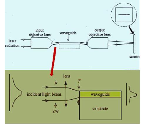
48 Prism Coupling (a) Prism coupling assembly; (b) phase-matching condition at prism waveguide interface; (c) rotation spectra against angle of incidence θ of the prism.
49 Prism Coupling where np is the prism index, θp is the prism angle, and θ is the measured incident angle for mode m ¼ 0, 1,.... The following factors limit the utilization of the prism coupling technique: (a) The film must be thick enough to permit the propagation of at least two modes. (b) The method is a contact method and it is necessary to press the film against the base of the prism. Extra care must be taken when measuring polymers. In general, the technique is non destructive. (c) Alignment of small samples with the coupling spot requires a certain degree of skill and experience. Typically, the laser spot is collimated to approximately 1.0 mm 2 and this can be a challenge where the proton beam written samples are only about 2.0 mm 2 in size.

50 M-Line Spectroscopy (MLS)
51 M-Line Spectroscopy (MLS) The refractive index (n f ) and thickness (T) of the thin film can be calculated using the step-index model: If the agreement between experimental and calculated values of N m is in the range of or less, the step-index model is satisfied.
52 Coupling Techniques For an integrated optical waveguide system, It is necessary to find a technique to effectively confine and couple the laser beam with the waveguide. Several techniques have been used, including prism coupling, end coupling, tapered and/or lunch coupling, and grating coupling.

53 Prism Coupling Method
54 End-Coupling Method

55 Lunch and Tapered-Coupling Method

56 Grating Coupling Method
57 Optical Loss where I 0 is the initial power, I(x) is the transmitted power through the waveguide at a distance x (cm), and α is defined as the attenuation coefficient of the waveguide, measured in decibels per centimeter (db/cm). The loss, L in decibels (db) is defined as: Many factors are considered to disturb the light propagation and increase the propagation losses: (a) Radiation losses due to the guided mode converse to the radiation mode. (b) Mode conversion losses due to conversion from the excited mode to other guided modes (c) Absorption losses due to light absorption in the waveguide materials.
 Tunneling losses that only occurs in barrier optical waveguides produced by ion modification Measurement of")
58 (d) Diffusion losses or scattering losses due to the imperfection of the waveguide structure. (e) Tunneling losses that only occurs in barrier optical waveguides produced by ion modification Measurement of Propagation Losses Cutback Method

59 WAVEGUIDE DEVICES
60 WAVEGUIDE DEVICES

61 WAVEGUIDE DEVICES

62 WAVEGUIDE DEVICES

63 WAVEGUIDE DEVICES
64 WAVEGUIDE DEVICES Can be wavelength selective/nonselective Up to N =M = 64, typically N, M < 10
65 WAVEGUIDE DEVICES
66 WAVEGUIDE DEVICES

67 WAVEGUIDE DEVICES
68 WAVEGUIDE DEVICES
OPTI510R: Photonics. Khanh Kieu College of Optical Sciences, University of Arizona Meinel building R.626
 OPTI510R: Photonics Khanh Kieu College of Optical Sciences, University of Arizona kkieu@optics.arizona.edu Meinel building R.626 Announcements Homework #3 is due today No class Monday, Feb 26 Pre-record
Waveguides and Optical Fibers
 Waveguides and Optical Fibers Dielectric Waveguides Light Light Light n n Light n > n A planar dielectric waveguide has a central rectangular region of higher refractive index n than the surrounding region
Principles of Optics for Engineers
 Principles of Optics for Engineers Uniting historically different approaches by presenting optical analyses as solutions of Maxwell s equations, this unique book enables students and practicing engineers
DIELECTRIC WAVEGUIDES and OPTICAL FIBERS
 DIELECTRIC WAVEGUIDES and OPTICAL FIBERS Light Light Light n 2 n 2 Light n 1 > n 2 A planar dielectric waveguide has a central rectangular region of higher refractive index n 1 than the surrounding region
Index. Cambridge University Press Silicon Photonics Design Lukas Chrostowski and Michael Hochberg. Index.
 absorption, 69 active tuning, 234 alignment, 394 396 apodization, 164 applications, 7 automated optical probe station, 389 397 avalanche detector, 268 back reflection, 164 band structures, 30 bandwidth
Guided Propagation Along the Optical Fiber. Xavier Fernando Ryerson University
 Guided Propagation Along the Optical Fiber Xavier Fernando Ryerson University The Nature of Light Quantum Theory Light consists of small particles (photons) Wave Theory Light travels as a transverse electromagnetic
Guided Propagation Along the Optical Fiber. Xavier Fernando Ryerson Comm. Lab
 Guided Propagation Along the Optical Fiber Xavier Fernando Ryerson Comm. Lab The Nature of Light Quantum Theory Light consists of small particles (photons) Wave Theory Light travels as a transverse electromagnetic
Hybrid Integration Technology of Silicon Optical Waveguide and Electronic Circuit
 Hybrid Integration Technology of Silicon Optical Waveguide and Electronic Circuit Daisuke Shimura Kyoko Kotani Hiroyuki Takahashi Hideaki Okayama Hiroki Yaegashi Due to the proliferation of broadband services
Guided Propagation Along the Optical Fiber
 Guided Propagation Along the Optical Fiber The Nature of Light Quantum Theory Light consists of small particles (photons) Wave Theory Light travels as a transverse electromagnetic wave Ray Theory Light
New Waveguide Fabrication Techniques for Next-generation PLCs
 New Waveguide Fabrication Techniques for Next-generation PLCs Masaki Kohtoku, Toshimi Kominato, Yusuke Nasu, and Tomohiro Shibata Abstract New waveguide fabrication techniques will be needed to make highly
Fabrication Techniques of Optical ICs
 Fabrication Techniques of Optical ICs Processing Techniques Lift off Process Etching Process Patterning Techniques Photo Lithography Electron Beam Lithography Photo Resist ( Microposit MP1300) Electron
Realization of Polarization-Insensitive Optical Polymer Waveguide Devices
 644 Realization of Polarization-Insensitive Optical Polymer Waveguide Devices Kin Seng Chiang,* Sin Yip Cheng, Hau Ping Chan, Qing Liu, Kar Pong Lor, and Chi Kin Chow Department of Electronic Engineering,
Supplementary Figure 1. GO thin film thickness characterization. The thickness of the prepared GO thin
 Supplementary Figure 1. GO thin film thickness characterization. The thickness of the prepared GO thin film is characterized by using an optical profiler (Bruker ContourGT InMotion). Inset: 3D optical
Robert G. Hunsperger. Integrated Optics. Theory and Technology. Sixth Edition. 4ü Spri rineer g<
 Robert G. Hunsperger Integrated Optics Theory and Technology Sixth Edition 4ü Spri rineer g< 1 Introduction 1 1.1 Advantages of Integrated Optics 2 1.1.1 Comparison of Optical Fibers with Other Interconnectors
Chapter 1 Silicon Photonic Wire Waveguides: Fundamentals and Applications
 Chapter 1 Silicon Photonic Wire Waveguides: Fundamentals and Applications Koji Yamada Abstract This chapter reviews the fundamental characteristics and basic applications of the silicon photonic wire waveguide.
 Chapter 5 5.1 What are the factors that determine the thickness of a polystyrene waveguide formed by spinning a solution of dissolved polystyrene onto a substrate? density of polymer concentration of polymer
Microphotonics Readiness for Commercial CMOS Manufacturing. Marco Romagnoli
 Microphotonics Readiness for Commercial CMOS Manufacturing Marco Romagnoli MicroPhotonics Consortium meeting MIT, Cambridge October 15 th, 2012 Passive optical structures based on SOI technology Building
E LECTROOPTICAL(EO)modulatorsarekeydevicesinoptical
modulatorsarekeydevicesinoptical") 286 JOURNAL OF LIGHTWAVE TECHNOLOGY, VOL. 26, NO. 2, JANUARY 15, 2008 Design and Fabrication of Sidewalls-Extended Electrode Configuration for Ridged Lithium Niobate Electrooptical Modulator Yi-Kuei Wu,
286 JOURNAL OF LIGHTWAVE TECHNOLOGY, VOL. 26, NO. 2, JANUARY 15, 2008 Design and Fabrication of Sidewalls-Extended Electrode Configuration for Ridged Lithium Niobate Electrooptical Modulator Yi-Kuei Wu,
Optical behavior. Reading assignment. Topic 10
 Reading assignment Optical behavior Topic 10 Askeland and Phule, The Science and Engineering of Materials, 4 th Ed.,Ch. 0. Shackelford, Materials Science for Engineers, 6 th Ed., Ch. 16. Chung, Composite
Chapter 9 GUIDED WAVE OPTICS
 [Reading Assignment, Hecht 5.6] Chapter 9 GUIDED WAVE OPTICS Optical fibers The step index circular waveguide is the most common fiber design for optical communications plastic coating (sheath) core cladding
Optical Polarization Filters and Splitters Based on Multimode Interference Structures using Silicon Waveguides
 International Journal of Engineering and Technology Volume No. 7, July, 01 Optical Polarization Filters and Splitters Based on Multimode Interference Structures using Silicon Waveguides 1 Trung-Thanh Le,
1. Evolution Of Fiber Optic Systems
 OPTICAL FIBER COMMUNICATION UNIT-I : OPTICAL FIBERS STRUCTURE: 1. Evolution Of Fiber Optic Systems The operating range of optical fiber system term and the characteristics of the four key components of
Transmitting Light: Fiber-optic and Free-space Communications Holography
 1 Lecture 9 Transmitting Light: Fiber-optic and Free-space Communications Holography 2 Wireless Phone Calls http://havilandtelconews.com/2011/10/the-reality-behind-wireless-networks/ 3 Undersea Cable and
Fundamentals of Electromagnetics With Engineering Applications by Stuart M. Wentworth Copyright 2005 by John Wiley & Sons. All rights reserved.
 Figure 7-1 (p. 339) Non-TEM mmode waveguide structures include (a) rectangular waveguide, (b) circular waveguide., (c) dielectric slab waveguide, and (d) fiber optic waveguide. Figure 7-2 (p. 340) Cross
(A) 2f (B) 2 f (C) f ( D) 2 (E) 2
 2f (B) 2 f (C) f ( D) 2 (E) 2") 1. A small vibrating object S moves across the surface of a ripple tank producing the wave fronts shown above. The wave fronts move with speed v. The object is traveling in what direction and with what
1. A small vibrating object S moves across the surface of a ripple tank producing the wave fronts shown above. The wave fronts move with speed v. The object is traveling in what direction and with what
Optical systems have carrier frequencies of ~100 THz. This corresponds to wavelengths from µm.
 Introduction A communication system transmits information form one place to another. This could be from one building to another or across the ocean(s). Many systems use an EM carrier wave to transmit information.
Simulation of technologically relevant SPR devices
 Simulation of technologically relevant SPR devices Author: Judith Costa Iracheta Advisor: Mauricio Moreno Sereno Facultat de Física, Universitat de Barcelona, Diagonal 645, 08028 Barcelona, Spain*. Abstract:
Examination Optoelectronic Communication Technology. April 11, Name: Student ID number: OCT1 1: OCT 2: OCT 3: OCT 4: Total: Grade:
 Examination Optoelectronic Communication Technology April, 26 Name: Student ID number: OCT : OCT 2: OCT 3: OCT 4: Total: Grade: Declaration of Consent I hereby agree to have my exam results published on
Tunable Color Filters Based on Metal-Insulator-Metal Resonators
 Chapter 6 Tunable Color Filters Based on Metal-Insulator-Metal Resonators 6.1 Introduction In this chapter, we discuss the culmination of Chapters 3, 4, and 5. We report a method for filtering white light
Lecture 5. SPR Sensors: Principle and Instrumentation.
 Lecture 5 Optical sensors. SPR Sensors: Principle and Instrumentation. t ti Optical sensors What they can be based on: Absorption spectroscopy (UV-VIS, VIS IR) Fluorescence/phosphorescence spectroscopy
Waveguiding in PMMA photonic crystals
 ROMANIAN JOURNAL OF INFORMATION SCIENCE AND TECHNOLOGY Volume 12, Number 3, 2009, 308 316 Waveguiding in PMMA photonic crystals Daniela DRAGOMAN 1, Adrian DINESCU 2, Raluca MÜLLER2, Cristian KUSKO 2, Alex.
Lecture: Integration of silicon photonics with electronics. Prepared by Jean-Marc FEDELI CEA-LETI
 Lecture: Integration of silicon photonics with electronics Prepared by Jean-Marc FEDELI CEA-LETI Context The goal is to give optical functionalities to electronics integrated circuit (EIC) The objectives
CHAPTER 2 POLARIZATION SPLITTER- ROTATOR BASED ON A DOUBLE- ETCHED DIRECTIONAL COUPLER
 CHAPTER 2 POLARIZATION SPLITTER- ROTATOR BASED ON A DOUBLE- ETCHED DIRECTIONAL COUPLER As we discussed in chapter 1, silicon photonics has received much attention in the last decade. The main reason is
OPTICAL GUIDED WAVES AND DEVICES
 OPTICAL GUIDED WAVES AND DEVICES Richard Syms John Cozens Department of Electrical and Electronic Engineering Imperial College of Science, Technology and Medicine McGRAW-HILL BOOK COMPANY London New York
CHIRPED FIBER BRAGG GRATING (CFBG) BY ETCHING TECHNIQUE FOR SIMULTANEOUS TEMPERATURE AND REFRACTIVE INDEX SENSING
 BY ETCHING TECHNIQUE FOR SIMULTANEOUS TEMPERATURE AND REFRACTIVE INDEX SENSING") CHIRPED FIBER BRAGG GRATING (CFBG) BY ETCHING TECHNIQUE FOR SIMULTANEOUS TEMPERATURE AND REFRACTIVE INDEX SENSING Siti Aisyah bt. Ibrahim and Chong Wu Yi Photonics Research Center Department of Physics,
CHIRPED FIBER BRAGG GRATING (CFBG) BY ETCHING TECHNIQUE FOR SIMULTANEOUS TEMPERATURE AND REFRACTIVE INDEX SENSING Siti Aisyah bt. Ibrahim and Chong Wu Yi Photonics Research Center Department of Physics,
Horizontal single and multiple slot waveguides: optical transmission at λ = 1550 nm
 Horizontal single and multiple slot waveguides: optical transmission at λ = 1550 nm Rong Sun 1 *, Po Dong 2 *, Ning-ning Feng 1, Ching-yin Hong 1, Jurgen Michel 1, Michal Lipson 2, Lionel Kimerling 1 1Department
Photograph of the rectangular waveguide components
 Waveguides Photograph of the rectangular waveguide components BACKGROUND A transmission line can be used to guide EM energy from one point (generator) to another (load). A transmission line can support
Optical Interconnection in Silicon LSI
 The Fifth Workshop on Nanoelectronics for Tera-bit Information Processing, 1 st Century COE, Hiroshima University Optical Interconnection in Silicon LSI Shin Yokoyama, Yuichiro Tanushi, and Masato Suzuki
LOS 1 LASER OPTICS SET
 LOS 1 LASER OPTICS SET Contents 1 Introduction 3 2 Light interference 5 2.1 Light interference on a thin glass plate 6 2.2 Michelson s interferometer 7 3 Light diffraction 13 3.1 Light diffraction on a
Optodevice Data Book ODE I. Rev.9 Mar Opnext Japan, Inc.
 Optodevice Data Book ODE-408-001I Rev.9 Mar. 2003 Opnext Japan, Inc. Section 1 Operating Principles 1.1 Operating Principles of Laser Diodes (LDs) and Infrared Emitting Diodes (IREDs) 1.1.1 Emitting Principles
The electric field for the wave sketched in Fig. 3-1 can be written as
 ELECTROMAGNETIC WAVES Light consists of an electric field and a magnetic field that oscillate at very high rates, of the order of 10 14 Hz. These fields travel in wavelike fashion at very high speeds.
Integrated electro-optical waveguide based devices with liquid crystals on a silicon backplane
 Integrated electro-optical waveguide based devices with liquid crystals on a silicon backplane Florenta Costache Group manager Smart Micro-Optics SMO/AMS Fraunhofer Institute for Photonic Microsystems,
Optical Fibers p. 1 Basic Concepts p. 1 Step-Index Fibers p. 2 Graded-Index Fibers p. 4 Design and Fabrication p. 6 Silica Fibers p.
 Preface p. xiii Optical Fibers p. 1 Basic Concepts p. 1 Step-Index Fibers p. 2 Graded-Index Fibers p. 4 Design and Fabrication p. 6 Silica Fibers p. 6 Plastic Optical Fibers p. 9 Microstructure Optical
ABSTRACT 1. INTRODUCTION
 Reflectance Fabry-Perot modulator utilizing electro-optic ZnO thin film Vikash Gulia* and Sanjeev Kumar Department of Physics and Astrophysics, University of Delhi, Delhi-117, India. *E-mail: vikasgulia222@rediffmail.com
Applications of Cladding Stress Induced Effects for Advanced Polarization Control in Silicon Photonics
 PIERS ONLINE, VOL. 3, NO. 3, 27 329 Applications of Cladding Stress Induced Effects for Advanced Polarization Control in licon Photonics D.-X. Xu, P. Cheben, A. Delâge, S. Janz, B. Lamontagne, M.-J. Picard
A tunable Si CMOS photonic multiplexer/de-multiplexer
 A tunable Si CMOS photonic multiplexer/de-multiplexer OPTICS EXPRESS Published : 25 Feb 2010 MinJae Jung M.I.C.S Content 1. Introduction 2. CMOS photonic 1x4 Si ring multiplexer Principle of add/drop filter
Optics Communications
 Optics Communications 283 (2010) 3678 3682 Contents lists available at ScienceDirect Optics Communications journal homepage: www.elsevier.com/locate/optcom Ultra-low-loss inverted taper coupler for silicon-on-insulator
Grating-waveguide structures and their applications in high-power laser systems
 Grating-waveguide structures and their applications in high-power laser systems Marwan Abdou Ahmed*, Martin Rumpel, Tom Dietrich, Stefan Piehler, Benjamin Dannecker, Michael Eckerle, and Thomas Graf Institut
Waveguide Bragg Gratings and Resonators LUMERICAL SOLUTIONS INC
 Waveguide Bragg Gratings and Resonators JUNE 2016 1 Outline Introduction Waveguide Bragg gratings Background Simulation challenges and solutions Photolithography simulation Initial design with FDTD Band
A STUDY OF THE LASER DIRECT WRITING FOR ALL POLYMER SINGLE MODE PASSIVE OPTICAL CHANNEL WAVEGUIDE DEVICES. Bradley W. Borden, B.S.
 A STUDY OF THE LASER DIRECT WRITING FOR ALL POLYMER SINGLE MODE PASSIVE OPTICAL CHANNEL WAVEGUIDE DEVICES Bradley W. Borden, B.S. Thesis Prepared for the Degree of MASTER OF SCIENCE UNIVERSITY OF NORTH
On-chip Si-based Bragg cladding waveguide with high index contrast bilayers
 On-chip Si-based Bragg cladding waveguide with high index contrast bilayers Yasha Yi, Shoji Akiyama, Peter Bermel, Xiaoman Duan, and L. C. Kimerling Massachusetts Institute of Technology, 77 Massachusetts
Novel Optical Waveguide Design Based on Wavefront Matching Method
 Novel Optical Waveguide Design Based on Wavefront Matching Method Hiroshi Takahashi, Takashi Saida, Yohei Sakamaki, and Toshikazu Hashimoto Abstract The wavefront matching method provides a new way to
Department of Electrical Engineering and Computer Science
 MASSACHUSETTS INSTITUTE of TECHNOLOGY Department of Electrical Engineering and Computer Science 6.161/6637 Practice Quiz 2 Issued X:XXpm 4/XX/2004 Spring Term, 2004 Due X:XX+1:30pm 4/XX/2004 Please utilize
Introduction Fundamentals of laser Types of lasers Semiconductor lasers
 ECE 5368 Introduction Fundamentals of laser Types of lasers Semiconductor lasers Introduction Fundamentals of laser Types of lasers Semiconductor lasers How many types of lasers? Many many depending on
Photonic Crystal Slot Waveguide Spectrometer for Detection of Methane
 Photonic Crystal Slot Waveguide Spectrometer for Detection of Methane Swapnajit Chakravarty 1, Wei-Cheng Lai 2, Xiaolong (Alan) Wang 1, Che-Yun Lin 2, Ray T. Chen 1,2 1 Omega Optics, 10306 Sausalito Drive,
Chapter Ray and Wave Optics
 109 Chapter Ray and Wave Optics 1. An astronomical telescope has a large aperture to [2002] reduce spherical aberration have high resolution increase span of observation have low dispersion. 2. If two
Infrared broadband 50%-50% beam splitters for s- polarized light
 University of New Orleans ScholarWorks@UNO Electrical Engineering Faculty Publications Department of Electrical Engineering 7-1-2006 Infrared broadband 50%-50% beam splitters for s- polarized light R.
Design and Simulation of Optical Power Splitter By using SOI Material
 J. Pure Appl. & Ind. Phys. Vol.3 (3), 193-197 (2013) Design and Simulation of Optical Power Splitter By using SOI Material NAGARAJU PENDAM * and C P VARDHANI 1 * Research Scholar, Department of Physics,
Projects in microwave theory 2009
 Electrical and information technology Projects in microwave theory 2009 Write a short report on the project that includes a short abstract, an introduction, a theory section, a section on the results and
MICRO RING MODULATOR. Dae-hyun Kwon. High-speed circuits and Systems Laboratory
 MICRO RING MODULATOR Dae-hyun Kwon High-speed circuits and Systems Laboratory Paper preview Title of the paper Low Vpp, ultralow-energy, compact, high-speed silicon electro-optic modulator Publication
Chapter 17: Wave Optics. What is Light? The Models of Light 1/11/13
 Chapter 17: Wave Optics Key Terms Wave model Ray model Diffraction Refraction Fringe spacing Diffraction grating Thin-film interference What is Light? Light is the chameleon of the physical world. Under
OPAC 202 Optical Design and Instrumentation. Topic 3 Review Of Geometrical and Wave Optics. Department of
 OPAC 202 Optical Design and Instrumentation Topic 3 Review Of Geometrical and Wave Optics Department of http://www.gantep.edu.tr/~bingul/opac202 Optical & Acustical Engineering Gaziantep University Feb
InP-based Waveguide Photodetector with Integrated Photon Multiplication
 InP-based Waveguide Photodetector with Integrated Photon Multiplication D.Pasquariello,J.Piprek,D.Lasaosa,andJ.E.Bowers Electrical and Computer Engineering Department University of California, Santa Barbara,
Photonics and Optical Communication
 Photonics and Optical Communication (Course Number 300352) Spring 2007 Dr. Dietmar Knipp Assistant Professor of Electrical Engineering http://www.faculty.iu-bremen.de/dknipp/ 1 Photonics and Optical Communication
plasmonic nanoblock pair
 Nanostructured potential of optical trapping using a plasmonic nanoblock pair Yoshito Tanaka, Shogo Kaneda and Keiji Sasaki* Research Institute for Electronic Science, Hokkaido University, Sapporo 1-2,
Substrate-Embedded and Flip-Chip-Bonded Photodetector Polymer-Based Optical Interconnects: Analysis, Design, and Performance
 2382 JOURNAL OF LIGHTWAVE TECHNOLOGY, VOL. 21, NO. 10, OCTOBER 2003 Substrate-Embedded and Flip-Chip-Bonded Photodetector Polymer-Based Optical Interconnects: Analysis, Design, and Performance Elias N.
Absorption: in an OF, the loss of Optical power, resulting from conversion of that power into heat.
 Absorption: in an OF, the loss of Optical power, resulting from conversion of that power into heat. Scattering: The changes in direction of light confined within an OF, occurring due to imperfection in
AS Physics Unit 5 - Waves 1
 AS Physics Unit 5 - Waves 1 WHAT IS WAVE MOTION? The wave motion is a means of transferring energy from one point to another without the transfer of any matter between the points. Waves may be classified
Impact of the light coupling on the sensing properties of photonic crystal cavity modes Kumar Saurav* a,b, Nicolas Le Thomas a,b,
 Impact of the light coupling on the sensing properties of photonic crystal cavity modes Kumar Saurav* a,b, Nicolas Le Thomas a,b, a Photonics Research Group, Ghent University-imec, Technologiepark-Zwijnaarde
Lecture 3. Mass sensors Optical sensors. SPR Sensors.
 Lecture 3 Mass sensors Optical sensors. SPR Sensors. Lecture plan mass sensors (QCM, SAW, u-cantilevers) thermal sensors optical sensors: adsorption diffractive index change SPR history concept performance
Silicon photonics with low loss and small polarization dependency. Timo Aalto VTT Technical Research Centre of Finland
 Silicon photonics with low loss and small polarization dependency Timo Aalto VTT Technical Research Centre of Finland EPIC workshop in Tokyo, 9 th November 2017 VTT Technical Research Center of Finland
Fiber Optic Communications Communication Systems
 INTRODUCTION TO FIBER-OPTIC COMMUNICATIONS A fiber-optic system is similar to the copper wire system in many respects. The difference is that fiber-optics use light pulses to transmit information down
Frequency Tunable Low-Cost Microwave Absorber for EMI/EMC Application
 Progress In Electromagnetics Research Letters, Vol. 74, 47 52, 2018 Frequency Tunable Low-Cost Microwave Absorber for EMI/EMC Application Gobinda Sen * and Santanu Das Abstract A frequency tunable multi-layer
Numerical Analysis and Optimization of a Multi-Mode Interference Polarization Beam Splitter
 Numerical Analysis and Optimization of a Multi-Mode Interference Polarization Beam Splitter Y. D Mello*, J. Skoric, M. Hui, E. Elfiky, D. Patel, D. Plant Department of Electrical Engineering, McGill University,
This writeup is adapted from Fall 2002, final project report for by Robert Winsor.
 Optical Waveguides in Andreas G. Andreou This writeup is adapted from Fall 2002, final project report for 520.773 by Robert Winsor. September, 2003 ABSTRACT This lab course is intended to give students
ECSE 352: Electromagnetic Waves
 December 2008 Final Examination ECSE 352: Electromagnetic Waves 09:00 12:00, December 15, 2008 Examiner: Zetian Mi Associate Examiner: Andrew Kirk Student Name: McGill ID: Instructions: This is a CLOSED
Silicon Photonic Device Based on Bragg Grating Waveguide
 Silicon Photonic Device Based on Bragg Grating Waveguide Hwee-Gee Teo, 1 Ming-Bin Yu, 1 Guo-Qiang Lo, 1 Kazuhiro Goi, 2 Ken Sakuma, 2 Kensuke Ogawa, 2 Ning Guan, 2 and Yong-Tsong Tan 2 Silicon photonics
Lateral leakage of TM-like mode in thin-ridge Silicon-on-Insulator bent waveguides and ring resonators
 Lateral leakage of TM-like mode in thin-ridge Silicon-on-Insulator bent waveguides and ring resonators Thach G. Nguyen *, Ravi S. Tummidi 2, Thomas L. Koch 2, and Arnan Mitchell School of Electrical and
ECE 6323 Ridge Waveguide Laser homework
 ECE 633 Ridge Waveguide Laser homework Introduction This is a slide from a lecture we will study later on. It is about diode lasers. Although we haven t studied diode lasers, there is one aspect about
Optical Fiber Technology. Photonic Network By Dr. M H Zaidi
 Optical Fiber Technology Numerical Aperture (NA) What is numerical aperture (NA)? Numerical aperture is the measure of the light gathering ability of optical fiber The higher the NA, the larger the core
Optical Splitters Based on Self-Imaging Effect in Multi-Mode Waveguide Made by Ion Exchange in Glass
 352 O. BARKMAN, V. JEŘÁBEK, V. PRAJZLER, OPTICAL SPLITTERS BASED ON SELF-IMAGING EFFECT IN MULTI-MODE Optical Splitters Based on Self-Imaging Effect in Multi-Mode Waveguide Made by Ion Exchange in Glass
Fiber-Optic Polarizer Using Resonant Tunneling through a Multilayer Overlay
 Fiber-Optic Polarizer Using Resonant Tunneling through a Multilayer Overlay Arun Kumar, Rajeev Jindal, and R. K. Varshney Department of Physics, Indian Institute of Technology, New Delhi 110 016 India
Design and Analysis of Resonant Leaky-mode Broadband Reflectors
 846 PIERS Proceedings, Cambridge, USA, July 6, 8 Design and Analysis of Resonant Leaky-mode Broadband Reflectors M. Shokooh-Saremi and R. Magnusson Department of Electrical and Computer Engineering, University
Integrated photonic circuit in silicon on insulator for Fourier domain optical coherence tomography
 Integrated photonic circuit in silicon on insulator for Fourier domain optical coherence tomography Günay Yurtsever *,a, Pieter Dumon a, Wim Bogaerts a, Roel Baets a a Ghent University IMEC, Photonics
UC Santa Barbara UC Santa Barbara Previously Published Works
 UC Santa Barbara UC Santa Barbara Previously Published Works Title Compact broadband polarizer based on shallowly-etched silicon-on-insulator ridge optical waveguides Permalink https://escholarship.org/uc/item/959523wq
Ti: LiNbO 3 Acousto-Optic Tunable Filter (AOTF)
") UDC 621.372.54:621.391.6 Ti: LiNbO 3 Acousto-Optic Tunable Filter (AOTF) VTadao Nakazawa VShinji Taniguchi VMinoru Seino (Manuscript received April 3, 1999) We have developed the following new elements
UDC 621.372.54:621.391.6 Ti: LiNbO 3 Acousto-Optic Tunable Filter (AOTF) VTadao Nakazawa VShinji Taniguchi VMinoru Seino (Manuscript received April 3, 1999) We have developed the following new elements
Angela Piegari ENEA, Optical Coatings Laboratory, Roma, Italy
 Optical Filters for Space Instrumentation Angela Piegari ENEA, Optical Coatings Laboratory, Roma, Italy Trieste, 18 February 2015 Optical Filters Optical Filters are commonly used in Space instruments
Fiber Optic Communication Systems. Unit-04: Theory of Light. https://sites.google.com/a/faculty.muet.edu.pk/abdullatif
 Unit-04: Theory of Light https://sites.google.com/a/faculty.muet.edu.pk/abdullatif Department of Telecommunication, MUET UET Jamshoro 1 Limitations of Ray theory Ray theory describes only the direction
Propagation Mechanism
 Propagation Mechanism ELE 492 FUNDAMENTALS OF WIRELESS COMMUNICATIONS 1 Propagation Mechanism Simplest propagation channel is the free space: Tx free space Rx In a more realistic scenario, there may be
Plane wave excitation by taper array for optical leaky waveguide antenna
 LETTER IEICE Electronics Express, Vol.15, No.2, 1 6 Plane wave excitation by taper array for optical leaky waveguide antenna Hiroshi Hashiguchi a), Toshihiko Baba, and Hiroyuki Arai Graduate School of
Lecture 9 External Modulators and Detectors
 Optical Fibres and Telecommunications Lecture 9 External Modulators and Detectors Introduction Where are we? A look at some real laser diodes. External modulators Mach-Zender Electro-absorption modulators
Module 19 : WDM Components
 Module 19 : WDM Components Lecture : WDM Components - I Part - I Objectives In this lecture you will learn the following WDM Components Optical Couplers Optical Amplifiers Multiplexers (MUX) Insertion
Directional coupler (2 Students)
") Directional coupler (2 Students) The goal of this project is to make a 2 by 2 optical directional coupler with a defined power ratio for the two output branches. The directional coupler should be optimized
Directional coupler (2 Students) The goal of this project is to make a 2 by 2 optical directional coupler with a defined power ratio for the two output branches. The directional coupler should be optimized
Hiroshi Murata and Yasuyuki Okamura. 1. Introduction. 2. Waveguide Fabrication
 OptoElectronics Volume 2008, Article ID 654280, 4 pages doi:10.1155/2008/654280 Research Article Fabrication of Proton-Exchange Waveguide Using Stoichiometric itao 3 for Guided Wave Electrooptic Modulators
Will contain image distance after raytrace Will contain image height after raytrace
 Name: LASR 51 Final Exam May 29, 2002 Answer all questions. Module numbers are for guidance, some material is from class handouts. Exam ends at 8:20 pm. Ynu Raytracing The first questions refer to the
SUPPLEMENTARY INFORMATION Polarization response of nanowires à la carte
 * Correspondence to anna.fontcuberta-morral@epfl.ch SUPPLEMENTARY INFORMATION Polarization response of nanowires à la carte Alberto Casadei, Esther Alarcon Llado, Francesca Amaduzzi, Eleonora Russo-Averchi,
A Novel technique to measure propagation loss of optical waveguides. Abstract. I. Introduction
 A Novel technique to measure propagation loss of optical waveguides Samit Barai, ASelvarajan, T.Srinivas,T.Madhan and R. Fazludeen' Applied Photonics Lab, ECE Dept. Indian Institute of Science, Bangalore,
Ultra-Low-Loss Athermal AWG Module with a Large Number of Channels
 Ultra-Low-Loss Athermal AWG Module with a Large Number of Channels by Junichi Hasegawa * and Kazutaka Nara * There is an urgent need for an arrayed waveguide grating (AWG), the device ABSTRACT that handles
Experimental Competition
 37 th International Physics Olympiad Singapore 8 17 July 2006 Experimental Competition Wed 12 July 2006 Experimental Competition Page 2 List of apparatus and materials Label Component Quantity Label Component
Development of Vertical Spot Size Converter (SSC) with Low Coupling Loss Using 2.5%Δ Silica-Based Planar Lightwave Circuit
 with Low Coupling Loss Using 2.5%Δ Silica-Based Planar Lightwave Circuit") Development of Vertical Spot Size Converter (SSC) with Low Coupling Loss Using 2.5%Δ Silica-Based Planar Lightwave Circuit Yasuyoshi Uchida *, Hiroshi Kawashima *, and Kazutaka Nara * Recently, new planar
Development of Vertical Spot Size Converter (SSC) with Low Coupling Loss Using 2.5%Δ Silica-Based Planar Lightwave Circuit Yasuyoshi Uchida *, Hiroshi Kawashima *, and Kazutaka Nara * Recently, new planar