Wish you all Very Happy New Year
|
|
|
- Lizbeth Grant
- 5 years ago
- Views:
Transcription
1 Wish you all Very Happy New Year Course: Basic Electronics (EC21101) Course Instructors: Prof. Goutam Saha (Sec. 2), Prof. Shailendra K. Varshney (Sec. 1), Prof. Sudip Nag (Sec. 3 ), Prof. Debashish Sen (Sec. 4) MON(10:00-10:55), WED(08:00-08:55), WED(09:00-09:55), THURS(10:00-10:55) Contact skvarshney@ece.iitkgp.ernet.in basicelectronicst@gmail.com
2 Course Breakup Mid-Semester Examination : 30 Marks End-Semester Examination: 50 Marks TA: 20 Marks Two class Tests (14 marks) Tutorial (3 marks) Attendance and interaction in class (3 marks) Mid Semester Examination: Feb End-Semester Examination: April 2016
3 Course contents Signal, noise, system, RL, RC filter circuit etc., Intrinsic, extrinsic semiconductor, drift & diffusion current, p-n junction, forward bias/ reverse bias, I-V equation (without proof), diode model (ideal, piece wise linear etc), Zener diode characteristics; half wave, full wave rectifier, bridge rectifier, ripple, Zener diode circuit (voltage ref, regulation), filter, clipper, clamper, multi diode circuit BJT Basics, alpha-beta relation, I-V equation with different regions, DC circuit analysis, common emitter circuit with and without emitter resistor, BJT amplifier, load line, Q point, small signal equivalent circuit, common emitter amplifier (gain, input resistance, output resistance).
4 Course contents MOSFET basic structure, IV equation (no proof) with different regions, depletion mode, enhancement mode, channel length modulation, DC circuit analysis, common source circuit with and without source resistor MOSFET amplifier, load line, Q point, small signal equivalent circuit, common source amplifier (gain, input resistance, output resistance). OPAMP basic, virtual ground, ideal properties, inverting, non inverting, buffer, differential amplifier, CMRR (all these with ideal and non ideal OPAMP gain), integrator, differentiator. Digital electronics- number system, Digital gates (symbol, truth table), universal gate, sum of product, product of sum, Karnaugh map, RS/D/T Flip Flop.
5 References Donald A Neamen, Electronic Circuits- Analysis and Design Text book Sedra and Smith, Microelectronics Text book (some portion). Raza Vi, Fundamentals of Microelectronics, Reference book Milliman and Halikas, Microelectronics, Reference book


6 What is signal? Function that provides information about the behavior or attributes of some phenomenon -audio, video, speech, image, medical, muscial etc.


7 Brown, red, orange: 12x10 3 Ω

")
")
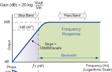
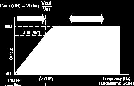
8 Filter Circuits Low pass (RC, RL) High Pass (CR, LR)

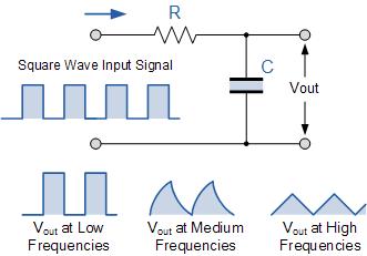
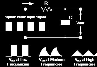
9 Filters as Integrator and Differentiator
10 Semiconductor physics


11 n-type Extrinsic semiconductors Group V elements P, As, Sb (donor) free electrons: majority (adding impurities to intrinsic semiconductors) p-type Group III elements B, Al, (acceptor) holes: majority Rough sketch of bandgap for n-type Rough sketch of bandgap for n-type
12 Carrier Transport Drift Movement caused by electric field Diffusion Flow caused by concentration gradient (due to non homogenous distribution)
13 Transport of free carriers in semiconductors Drift e - Random motion of carriers in semiconductors with and without field o Thermal motion of an individual electron random scattering (lattice vibration, impurities, other electrons, and defects) o no net motion of group of n electrons/cm 3 over any period of time J n

14 Diffusion Flow from region of high concentration to low concentration - concentration gradient Charge carriers in absence of electric field move toward region of low concentration More nonuniform the concentration, the larger the current
15 n : carrier concentration at given point along x Concentration gradient If each carrier has charge q, and the semiconductor has cross-section area A D n : diffusion constant (cm 2 /s) D n = 34 cm 2 /s (for electrons); D p =12 cm 2 /s (for holes) Current density (electrons) Current density (holes)
16 With both electron and hole gradients present, the total current density is Consider a situation as shown in figure below. Suppose the electron concentration is N at x=0 and falls linearly to zero at x=l. Determine the diffusion current.
17 L d is constant Make an analysis of both gradient profiles (linear and exponential) Exercise At what value of x does the current density drops to 1% of its maximum value?
18 Now, we can FINALLY write down the TOTAL current in a semiconductor: For electrons: J N = J N,drift + J N,diff = qnµ n ε + qd N dn dx For holes: J P = J P,drift + J P,diff = qpµ p ε qd P dp dx And TOTAL current:
19 Under equilibrium, or open circuit conditions, total current must always be zero J drift = -J diffusion J N = qnµ ε + qd n N dn dx = 0 Leads to the Einstein Relationship: D = µ kt q This is very, very important because it connects diffusivity with mobility, which we already know how to look up
20 pn junction Simplest semiconductor device Flow of current freely when p region has external positive voltage (forward bias) No current in reverse bias mode This asymmetry in current flows makes pn junction diodes useful as rectifier. Biased pn junction can be used Voltage variable capacitors Photocells Light emittters

21 What are we going to study.. No external connections Terminals are open p-type n-type A pn junction employs following doping levels, N a =10 16 cm -3, N d = cm -3. Calculate the electron and hole concentrations on the two sides. electrons holes
22 Evolution of junction with time t = t =t t = E in Junction reaches equilibrium once the electric field is strong enough to stop diffusion
23 Forward bias E A E in V f
24 Diode characteristics
25 No biasing p-region holes flow Reverse bias Bound charges electrons flow n-region p-region n-region E in E A V R
26 Peak Reverse Voltage (Peak Inverse Voltage): Voltage that may be applied to the junction without causing junction breakdown
27 Effect of temperature I s and V T are temperature dependent Diode characteristics will change with temperature Greater be the temperature, lower be the forward voltage required for the conduction of current. For Si, 2mV/ C
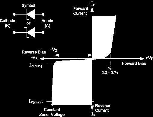
28 Breakdown in Diodes Zener breakdown Avalance breakdown
29 Zener breakdown Dominant for heavily doped (>10 18 cm -3 ) Depletion region becomes narrower Tunneling of carriers across the region Breakdown at a few volts (typically < 5 V)
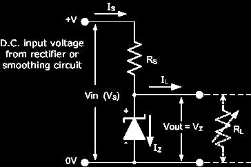
30 Zener diodes Diodes operated under Zener breakdown effect Can be used as voltage regulator
31 Avalanche breakdown More lightly doped junctions (< cm -3 ) Wider depletion region, electrons accelerated across it gain enough kinetic energy to create additional EHPs by breaking the covalent bonds Impact ionization and carrier multiplication V R > 7V Most common breakdown V BR ε 2 CR ε s 2qN if V BR >> V 0 V BR decreases with increasing N (=N A or N D ) V BR decreases with decreasing E G
32 Diodes in DC circuit Voltage and current designation Ideal I D -V D characteristics Forward bias Reverse bias
33
34 Half-wave Rectifiers
35
36 Full Wave Bridge Rectifier with Capacitor Filter
37
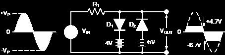
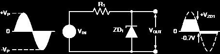
38 Diode as Clipper Also known as Diode limiter Wave shaping circuit that clips or slice certain portion of a input waveform Positive clipper Negative clipper Biased Positive clipper Biased negative clipper

39 Positive clipper Courtesy: circuitstoday.com
40 Courtesy: circuitstoday.com Negative clipper
41 Courtesy: circuitstoday.com Biased Positive Clipper
42 Courtesy: circuitstoday.com Biased Negative Clipper
43
44 Different clipping circuits
45
46
47
48
49
50 Diode as Clamper A clamping circuit is used to place either the positive or negative peak of a signal at a desired level. The dc component is simply added or subtracted to/from the input signal. The clamper is also referred to as an IC restorer and ac signal level shifter.
51
Intrinsic Semiconductor
 Semiconductors Crystalline solid materials whose resistivities are values between those of conductors and insulators. Good electrical characteristics and feasible fabrication technology are some reasons
IENGINEERS- CONSULTANTS QUESTION BANK SERIES ELECTRONICS ENGINEERING 1 YEAR UPTU
 ELECTRONICS ENGINEERING Unit 1 Objectives Q.1 The breakdown mechanism in a lightly doped p-n junction under reverse biased condition is called. (A) avalanche breakdown. (B) zener breakdown. (C) breakdown
Part II. Devices Diode, BJT, MOSFETs
 Part II Devices Diode, BJT, MOSFETs 49 4 Semiconductor Semiconductor The number of charge carriers available to conduct current 1 is between that of conductors and that of insulators. Semiconductor is
Ch5 Diodes and Diodes Circuits
 Circuits and Analog Electronics Ch5 Diodes and Diodes Circuits 5.1 The Physical Principles of Semiconductor 5.2 Diodes 5.3 Diode Circuits 5.4 Zener Diode References: Floyd-Ch2; Gao-Ch6; 5.1 The Physical
Department of Electrical Engineering IIT Madras
 Department of Electrical Engineering IIT Madras Sample Questions on Semiconductor Devices EE3 applicants who are interested to pursue their research in microelectronics devices area (fabrication and/or
Diode Limiters or Clipper Circuits
 Diode Limiters or Clipper Circuits Circuits which are used to clip off portions of signal voltages above or below certain levels are called limiters or clippers. Types of Clippers Positive Clipper Negative
Semiconductor Devices Lecture 5, pn-junction Diode
 Semiconductor Devices Lecture 5, pn-junction Diode Content Contact potential Space charge region, Electric Field, depletion depth Current-Voltage characteristic Depletion layer capacitance Diffusion capacitance
Digital Integrated Circuits A Design Perspective. The Devices. Digital Integrated Circuits 2nd Devices
 Digital Integrated Circuits A Design Perspective The Devices The Diode The diodes are rarely explicitly used in modern integrated circuits However, a MOS transistor contains at least two reverse biased
Basic Electronics Important questions
 Basic Electronics Important questions B.E-2/4 Mech- B Faculty: P.Lakshmi Prasanna Note: Read the questions in the following order i. Assignment questions ii. Class test iii. Expected questions iv. Tutorials
Electronic Circuits I. Instructor: Dr. Alaa Mahmoud
 Electronic Circuits I Instructor: Dr. Alaa Mahmoud alaa_y_emam@hotmail.com Chapter 27 Diode and diode application Outline: Semiconductor Materials The P-N Junction Diode Biasing P-N Junction Volt-Ampere
Difference between BJTs and FETs. Junction Field Effect Transistors (JFET)
") Difference between BJTs and FETs Transistors can be categorized according to their structure, and two of the more commonly known transistor structures, are the BJT and FET. The comparison between BJTs
Difference between BJTs and FETs Transistors can be categorized according to their structure, and two of the more commonly known transistor structures, are the BJT and FET. The comparison between BJTs
Lecture 4 -- Tuesday, Sept. 19: Non-uniform injection and/or doping. Diffusion. Continuity/conservation. The five basic equations.
 6.012 ELECTRONIC DEVICES AND CIRCUITS Schedule -- Fall 1995 (8/31/95 version) Recitation 1 -- Wednesday, Sept. 6: Review of 6.002 models for BJT. Discussion of models and modeling; motivate need to go
Chapter 2. Diodes & Applications
 Chapter 2 Diodes & Applications The Diode A diode is made from a small piece of semiconductor material, usually silicon, in which half is doped as a p region and half is doped as an n region with a pn
SRM INSTITUTE OF SCIENCE AND TECHNOLOGY (DEEMED UNIVERSITY)
") SRM INSTITUTE OF SCIENCE AND TECHNOLOGY (DEEMED UNIVERSITY) QUESTION BANK I YEAR B.Tech (II Semester) ELECTRONIC DEVICES (COMMON FOR EC102, EE104, IC108, BM106) UNIT-I PART-A 1. What are intrinsic and
SRM INSTITUTE OF SCIENCE AND TECHNOLOGY (DEEMED UNIVERSITY) QUESTION BANK I YEAR B.Tech (II Semester) ELECTRONIC DEVICES (COMMON FOR EC102, EE104, IC108, BM106) UNIT-I PART-A 1. What are intrinsic and
SEMICONDUCTOR ELECTRONICS: MATERIALS, DEVICES AND SIMPLE CIRCUITS. Class XII : PHYSICS WORKSHEET
 SEMICONDUCT ELECTRONICS: MATERIALS, DEVICES AND SIMPLE CIRCUITS Class XII : PHYSICS WKSHEET 1. How is a n-p-n transistor represented symbolically? (1) 2. How does conductivity of a semiconductor change
Analog Electronic Circuits
 Analog Electronic Circuits Chapter 1: Semiconductor Diodes Objectives: To become familiar with the working principles of semiconductor diode To become familiar with the design and analysis of diode circuits
Scheme I Sample. : Second : Basic. Electronics : 70. Marks. Time: 3 Hrs. 2] b) State any. e) State any. Figure Definition.
![Scheme I Sample. : Second : Basic. Electronics : 70. Marks. Time: 3 Hrs. 2] b) State any. e) State any. Figure Definition.](/thumbs/96/128002629.jpg "Scheme I Sample. : Second : Basic. Electronics : 70. Marks. Time: 3 Hrs. 2] b) State any. e) State any. Figure Definition.") Program Name Program Code Semester Course Title Scheme I Sample Question Paper : Diploma in Electronics Program Group : DE/EJ/IE/IS/ET/EN/EX : Second : Basic Electronics : 70 22216 Time: 3 Hrs. Instructions:
Program Name Program Code Semester Course Title Scheme I Sample Question Paper : Diploma in Electronics Program Group : DE/EJ/IE/IS/ET/EN/EX : Second : Basic Electronics : 70 22216 Time: 3 Hrs. Instructions:
ELEC 3908, Physical Electronics, Lecture 16. Bipolar Transistor Operation
 ELEC 3908, Physical Electronics, Lecture 16 Bipolar Transistor Operation Lecture Outline Last lecture discussed the structure and fabrication of a double diffused bipolar transistor Now examine current
QUESTION BANK EC6201 ELECTRONIC DEVICES UNIT I SEMICONDUCTOR DIODE PART A. It has two types. 1. Intrinsic semiconductor 2. Extrinsic semiconductor.
 FATIMA MICHAEL COLLEGE OF ENGINEERING & TECHNOLOGY Senkottai Village, Madurai Sivagangai Main Road, Madurai - 625 020. [An ISO 9001:2008 Certified Institution] QUESTION BANK EC6201 ELECTRONIC DEVICES SEMESTER:
Microelectronic Circuits Fourth Edition Adel S. Sedra, Kenneth C. Smith, 1998 Oxford University Press
 Diodes ELZ 206 - Elektronik I Microelectronic Circuits Fourth Edition Adel S. Sedra, Kenneth C. Smith, 1998 Oxford University Press Department of Electrical and Electronics Engineering Dicle University
Basic Electronics. Introductory Lecture Course for. Technology and Instrumentation in Particle Physics Chicago, Illinois June 9-14, 2011
 Basic Electronics Introductory Lecture Course for Technology and Instrumentation in Particle Physics 2011 Chicago, Illinois June 9-14, 2011 Presented By Gary Drake Argonne National Laboratory Session 3
1) A silicon diode measures a low value of resistance with the meter leads in both positions. The trouble, if any, is
 A silicon diode measures a low value of resistance with the meter leads in both positions. The trouble, if any, is") 1) A silicon diode measures a low value of resistance with the meter leads in both positions. The trouble, if any, is A [ ]) the diode is open. B [ ]) the diode is shorted to ground. C [v]) the diode is
1) A silicon diode measures a low value of resistance with the meter leads in both positions. The trouble, if any, is A [ ]) the diode is open. B [ ]) the diode is shorted to ground. C [v]) the diode is
Lecture -1: p-n Junction Diode
 Lecture -1: p-n Junction Diode Diode: A pure silicon crystal or germanium crystal is known as an intrinsic semiconductor. There are not enough free electrons and holes in an intrinsic semi-conductor to
BASIC ELECTRONICS ENGINEERING
 BASIC ELECTRONICS ENGINEERING Objective Questions UNIT 1: DIODES AND CIRCUITS 1 2 3 4 5 6 7 8 9 10 11 12 The process by which impurities are added to a pure semiconductor is A. Diffusing B. Drift C. Doping
Physics 160 Lecture 5. R. Johnson April 13, 2015
 Physics 160 Lecture 5 R. Johnson April 13, 2015 Half Wave Diode Rectifiers Full Wave April 13, 2015 Physics 160 2 Note that there is no ground connection on this side of the rectifier! Output Smoothing
Chapter 2 PN junction and diodes
 Chapter 2 PN junction and diodes ELEC-H402/CH2: PN junction and diodes 1 PN junction and diodes PN junction What happens in a PN junction Currents through the PN junction Properties of the depletion region
ECE 440 Lecture 29 : Introduction to the BJT-I Class Outline:
 ECE 440 Lecture 29 : Introduction to the BJT-I Class Outline: Narrow-Base Diode BJT Fundamentals BJT Amplification Things you should know when you leave Key Questions How does the narrow-base diode multiply
EDC Lecture Notes UNIT-1
 P-N Junction Diode EDC Lecture Notes Diode: A pure silicon crystal or germanium crystal is known as an intrinsic semiconductor. There are not enough free electrons and holes in an intrinsic semi-conductor
Lecture 2 p-n junction Diode characteristics. By Asst. Prof Dr. Jassim K. Hmood
 Electronic I Lecture 2 p-n junction Diode characteristics By Asst. Prof Dr. Jassim K. Hmood THE p-n JUNCTION DIODE The pn junction diode is formed by fabrication of a p-type semiconductor region in intimate
GUJARAT TECHNOLOGICAL UNIVERSITY BE - SEMESTER III EXAMINATION SUMMER 2013
 Seat No.: Enrolment No. GUJARAT TECHNOLOGICAL UNIVERSITY BE - SEMESTER III EXAMINATION SUMMER 2013 Subject Code: 131101 Date: 31-05-2013 Subject Name: Basic Electronics Time: 02.30 pm - 05.00 pm Total
Electronics The basics of semiconductor physics
 Electronics The basics of semiconductor physics Prof. Márta Rencz, Gábor Takács BME DED 17/09/2015 1 / 37 The basic properties of semiconductors Range of conductivity [Source: http://www.britannica.com]
I E I C since I B is very small
 Figure 2: Symbols and nomenclature of a (a) npn and (b) pnp transistor. The BJT consists of three regions, emitter, base, and collector. The emitter and collector are usually of one type of doping, while
Microelectronic Circuits, Kyung Hee Univ. Spring, Bipolar Junction Transistors
 Bipolar Junction Transistors 1 Introduction physical structure of the bipolar transistor and how it works How the voltage between two terminals of the transistor controls the current that flows through
Electronics Review Flashcards
 November 21, 2011 1 Op Amps 2 Diodes 3 Silicon 4 pn Junctions 5 BJTs 6 MOSFETs Open Loop Characteristics Open-Loop Op-Amp Characteristics (first-order model) Closed Loop Characteristics Closed-Loop Op-Amp
The shape of the waveform will be the same, but its level is shifted either upward or downward. The values of the resistor R and capacitor C affect
 Diode as Clamper A clamping circuit is used to place either the positive or negative peak of a signal at a desired level. The dc component is simply added or subtracted to/from the input signal. The clamper
CONTENTS. 2.2 Schrodinger's Wave Equation 31. PART I Semiconductor Material Properties. 2.3 Applications of Schrodinger's Wave Equation 34
 CONTENTS Preface x Prologue Semiconductors and the Integrated Circuit xvii PART I Semiconductor Material Properties CHAPTER 1 The Crystal Structure of Solids 1 1.0 Preview 1 1.1 Semiconductor Materials
R a) Draw and explain VI characteristics of Si & Ge diode. (8M) b) Explain the operation of SCR & its characteristics (8M)
 Draw and explain VI characteristics of Si & Ge diode. (8M) b) Explain the operation of SCR & its characteristics (8M)") SET - 1 1. a) Define i) transient capacitance ii) Diffusion capacitance (4M) b) Explain Fermi level in intrinsic and extrinsic semiconductor (4M) c) Derive the expression for ripple factor of Half wave
SET - 1 1. a) Define i) transient capacitance ii) Diffusion capacitance (4M) b) Explain Fermi level in intrinsic and extrinsic semiconductor (4M) c) Derive the expression for ripple factor of Half wave
EC T34 ELECTRONIC DEVICES AND CIRCUITS
 RAJIV GANDHI COLLEGE OF ENGINEERING AND TECHNOLOGY PONDY-CUDDALORE MAIN ROAD, KIRUMAMPAKKAM-PUDUCHERRY DEPARTMENT OF ECE EC T34 ELECTRONIC DEVICES AND CIRCUITS II YEAR Mr.L.ARUNJEEVA., AP/ECE 1 PN JUNCTION
Student Lecture by: Giangiacomo Groppi Joel Cassell Pierre Berthelot September 28 th 2004
 Student Lecture by: Giangiacomo Groppi Joel Cassell Pierre Berthelot September 28 th 2004 Lecture outline Historical introduction Semiconductor devices overview Bipolar Junction Transistor (BJT) Field
CHAPTER FORMULAS & NOTES
 Formulae For u SEMICONDUCTORS By Mir Mohammed Abbas II PCMB 'A' 1 Important Terms, Definitions & Formulae CHAPTER FORMULAS & NOTES 1 Intrinsic Semiconductor: The pure semiconductors in which the electrical
EC6202- ELECTRONIC DEVICES AND CIRCUITS UNIT TEST-1 EXPECTED QUESTIONS
 EC6202- ELECTRONIC DEVICES AND CIRCUITS UNIT TEST-1 EXPECTED QUESTIONS 1. List the PN diode parameters. 1. Bulk Resistance. 2. Static Resistance/Junction Resistance (or) DC Forward Resistance 3. Dynamic
Discuss the basic structure of atoms Discuss properties of insulators, conductors, and semiconductors
 Discuss the basic structure of atoms Discuss properties of insulators, conductors, and semiconductors Discuss covalent bonding Describe the properties of both p and n type materials Discuss both forward
Section 2.3 Bipolar junction transistors - BJTs
 Section 2.3 Bipolar junction transistors - BJTs Single junction devices, such as p-n and Schottkty diodes can be used to obtain rectifying I-V characteristics, and to form electronic switching circuits
Lesson Plan. Electronics 1-Total 51 Hours
 Lesson Plan. Electronics 1-Total 5s Unit I: Electrical Engineering materials:(10) Crystal structure & defects; Ceramic materials-structures, composites, processing and uses; Insulating laminates for electronics,
Diodes and Applications
 Diodes and Applications Diodes and Applications 2 1 Diode Operation 2 2 Voltage-Current (V-I) Characteristics 2 3 Diode Models 2 4 Half-Wave Rectifiers 2 5 Full-Wave Rectifiers 2 6 Power Supply Filters
OBJECTIVE TYPE QUESTIONS FOR PRACTICAL EXAMINATION Subject : Electronics-I ( EC 112)
") OBJECTIVE TYPE QUESTIONS FOR PRACTICAL EXAMINATION Subject : Electronics-I ( EC 112) 1. Which mathematical notation specifies the condition of periodicity for a continuous time signal? a. x(t) = x( t +T)
OBJECTIVE TYPE QUESTIONS FOR PRACTICAL EXAMINATION Subject : Electronics-I ( EC 112) 1. Which mathematical notation specifies the condition of periodicity for a continuous time signal? a. x(t) = x( t +T)
Module 04.(B1) Electronic Fundamentals
 Electronic Fundamentals") 1.1a. Semiconductors - Diodes. Module 04.(B1) Electronic Fundamentals Question Number. 1. What gives the colour of an LED?. Option A. The active element. Option B. The plastic it is encased in. Option
1.1a. Semiconductors - Diodes. Module 04.(B1) Electronic Fundamentals Question Number. 1. What gives the colour of an LED?. Option A. The active element. Option B. The plastic it is encased in. Option
UNIT IX ELECTRONIC DEVICES
 UNT X ELECTRONC DECES Weightage Marks : 07 Semiconductors Semiconductors diode-- characteristics in forward and reverse bias, diode as rectifier. - characteristics of LED, Photodiodes, solarcell and Zener
EJERCICIOS DE COMPONENTES ELECTRÓNICOS. 1 er cuatrimestre
 EJECICIOS DE COMPONENTES ELECTÓNICOS. 1 er cuatrimestre 2 o Ingeniería Electrónica Industrial Juan Antonio Jiménez Tejada Índice 1. Basic concepts of Electronics 1 2. Passive components 1 3. Semiconductors.
Reg. No. : Question Paper Code : B.E./B.Tech. DEGREE EXAMINATION, NOVEMBER/DECEMBER Second Semester
 WK 5 Reg. No. : Question Paper Code : 27184 B.E./B.Tech. DEGREE EXAMINATION, NOVEMBER/DECEMBER 2015. Time : Three hours Second Semester Electronics and Communication Engineering EC 6201 ELECTRONIC DEVICES
EC6202-ELECTRONIC DEVICES AND CIRCUITS YEAR/SEM: II/III UNIT 1 TWO MARKS. 1. Define diffusion current.
 EC6202-ELECTRONIC DEVICES AND CIRCUITS YEAR/SEM: II/III UNIT 1 TWO MARKS 1. Define diffusion current. A movement of charge carriers due to the concentration gradient in a semiconductor is called process
Università degli Studi di Roma Tor Vergata Dipartimento di Ingegneria Elettronica. Analogue Electronics. Paolo Colantonio A.A.
 Università degli Studi di Roma Tor Vergata Dipartimento di Ingegneria Elettronica Analogue Electronics Paolo Colantonio A.A. 2015-16 Introduction: materials Conductors e.g. copper or aluminum have a cloud
Basic Electronic Devices and Circuits EE 111 Electrical Engineering Majmaah University 2 nd Semester 1432/1433 H. Chapter 2. Diodes and Applications
 Basic Electronic Devices and Circuits EE 111 Electrical Engineering Majmaah University 2 nd Semester 1432/1433 H Chapter 2 Diodes and Applications 1 Diodes A diode is a semiconductor device with a single
Shankersinh Vaghela Bapu Institute of Technology INDEX
 Shankersinh Vaghela Bapu Institute of Technology Diploma EE Semester III 3330905: ELECTRONIC COMPONENTS AND CIRCUITS INDEX Sr. No. Title Page Date Sign Grade 1 Obtain I-V characteristic of Diode. 2 To
EE301 Electronics I , Fall
 EE301 Electronics I 2018-2019, Fall 1. Introduction to Microelectronics (1 Week/3 Hrs.) Introduction, Historical Background, Basic Consepts 2. Rewiev of Semiconductors (1 Week/3 Hrs.) Semiconductor materials
EE/COE 152: Basic Electronics. Lecture 3. A.S Agbemenu. https://sites.google.com/site/agbemenu/courses/ee-coe-152
 EE/COE 152: Basic Electronics Lecture 3 A.S Agbemenu https://sites.google.com/site/agbemenu/courses/ee-coe-152 Books: Microelcetronic Circuit Design (Jaeger/Blalock) Microelectronic Circuits (Sedra/Smith)
ECE 440 Lecture 39 : MOSFET-II
 ECE 440 Lecture 39 : MOSFETII Class Outline: MOSFET Qualitative Effective Mobility MOSFET Quantitative Things you should know when you leave Key Questions How does a MOSFET work? Why does the channel mobility
 Code No: Y0221/R07 Set No. 1 I B.Tech Supplementary Examinations, Apr/May 2013 BASIC ELECTRONIC DEVICES AND CIRCUITS (Electrical & Electronics Engineering) Time: 3 hours Max Marks: 80 Answer any FIVE Questions
Section:A Very short answer question
 Section:A Very short answer question 1.What is the order of energy gap in a conductor, semi conductor, and insulator?. Conductor - no energy gap Semi Conductor - It is of the order of 1 ev. Insulator -
Lesson 08. Name and affiliation of the author: Professor L B D R P Wijesundera Department of Physics, University of Kelaniya.
 Lesson 08 Title of the Experiment: Identification of active components in electronic circuits and characteristics of a Diode, Zener diode and LED (Activity number of the GCE Advanced Level practical Guide
UNIT I Introduction to DC & AC circuits
 SIDDHARTH GROUP OF INSTITUTIONS :: PUTTUR Siddharth Nagar, Narayanavanam Road 517583 QUESTION BANK (DESCRIPTIVE) Subject with Code: Basic Electrical and Electronics Engineering (16EE207) Year & Sem: II-B.
CENTURION UNIVERSITY OF TECHNOLOGY AND MANAGEMENT SCHOOL OF ENGINEERING & TECHNOLOGYDEPARTMENT OF ELECTRONICS & COMMUNICATION ENGINEERING
 CENTURION UNIVERSITY OF TECHNOLOGY AND MANAGEMENT SCHOOL OF ENGINEERING & TECHNOLOGYDEPARTMENT OF ELECTRONICS & COMMUNICATION ENGINEERING ELECTRONIC DEVICES Section: ECE SEM: II PART-A 1. a) In a N-type
10/27/2009 Reading: Chapter 10 of Hambley Basic Device Physics Handout (optional)
") EE40 Lec 17 PN Junctions Prof. Nathan Cheung 10/27/2009 Reading: Chapter 10 of Hambley Basic Device Physics Handout (optional) Slide 1 PN Junctions Semiconductor Physics of pn junctions (for reference
EE40 Lec 17 PN Junctions Prof. Nathan Cheung 10/27/2009 Reading: Chapter 10 of Hambley Basic Device Physics Handout (optional) Slide 1 PN Junctions Semiconductor Physics of pn junctions (for reference
 Energy band diagrams Metals: 9. ELECTRONIC DEVICES GIST ρ= 10-2 to 10-8 Ω m Insulators: ρ> 10 8 Ω m Semiconductors ρ= 1 to 10 5 Ω m 109 A. Intrinsic semiconductors At T=0k it acts as insulator At room
Analog Electronics (Course Code: EE314) Lecture 5 7: Junction contd, BJT. Course Instructor: Shree Prakash Tiwari
 Lecture 5 7: Junction contd, BJT. Course Instructor: Shree Prakash Tiwari") ndian nstitute of echnology Jodhpur, Year 2017 Analog lectronics (ourse ode: 314) Lecture 5 7: Junction contd, J ourse nstructor: Shree Prakash iwari mail: sptiwari@iitj.ac.in Webpage: http://home.iitj.ac.in/~sptiwari/
ndian nstitute of echnology Jodhpur, Year 2017 Analog lectronics (ourse ode: 314) Lecture 5 7: Junction contd, J ourse nstructor: Shree Prakash iwari mail: sptiwari@iitj.ac.in Webpage: http://home.iitj.ac.in/~sptiwari/
FINALTERM EXAMINATION. Spring PHY301- Circuit Theory
 Date 14/2/2013 Eini FINALTERM EXAMINATION Spring 2010 PHY301- Circuit Theory Time: 90 min Marks: 60 Question No: 1 If we connect 3 capacitors in parallel, the combined effect of all these capacitors will
Georgia Institute of Technology School of Electrical and Computer Engineering. Midterm Exam
 Georgia Institute of Technology School of Electrical and Computer Engineering Midterm Exam ECE-3400 Fall 2013 Tue, September 24, 2013 Duration: 80min First name Solutions Last name Solutions ID number
Carleton University. Faculty of Engineering and Design, Department of Electronics. ELEC 2507 Electronic - I Summer Term 2017
 Carleton University Faculty of Engineering and Design, Department of Electronics Instructors: ELEC 2507 Electronic - I Summer Term 2017 Name Section Office Email Prof. Q. J. Zhang Section A 4148 ME qjz@doe.carleton.ca
PN Junction in equilibrium
 PN Junction in equilibrium PN junctions are important for the following reasons: (i) PN junction is an important semiconductor device in itself and used in a wide variety of applications such as rectifiers,
SIDDHARTH GROUP OF INSTITUTIONS :: PUTTUR Siddharth Nagar, Narayanavanam Road QUESTION BANK (DESCRIPTIVE) PART - A
 PART - A") SIDDHARTH GROUP OF INSTITUTIONS :: PUTTUR Siddharth Nagar, Narayanavanam Road 517583 QUESTION BANK (DESCRIPTIVE) Subject with Code: Basic Electrical and Electronics Engineering (16EE207) Year & Sem: II-B.
SIDDHARTH GROUP OF INSTITUTIONS :: PUTTUR Siddharth Nagar, Narayanavanam Road 517583 QUESTION BANK (DESCRIPTIVE) Subject with Code: Basic Electrical and Electronics Engineering (16EE207) Year & Sem: II-B.
Basic Electronics SYLLABUS BASIC ELECTRONICS. Subject Code : 15ELN15/25 IA Marks : 20. Hrs/Week : 04 Exam Hrs. : 03. Total Hrs. : 50 Exam Marks : 80
 SYLLABUS BASIC ELECTRONICS Subject Code : /25 IA Marks : 20 Hrs/Week : 04 Exam Hrs. : 03 Total Hrs. : 50 Exam Marks : 80 Course objectives: The course objective is to make students of all the branches
 Electronic Devices 1. Current flowing in each of the following circuits A and respectively are: (Circuit 1) (Circuit 2) 1) 1A, 2A 2) 2A, 1A 3) 4A, 2A 4) 2A, 4A 2. Among the following one statement is not
Electronics I. Midterm #1
 EECS:3400 Electronics I s5ms_elct7.fm - Section Electronics I Midterm # Problems Points. 4 2. 5 3. 6 Total 5 Was the exam fair? yes no EECS:3400 Electronics I s5ms_elct7.fm - 2 Problem 4 points For full
Semiconductor Devices
 Semiconductor Devices Modelling and Technology Source Electrons Gate Holes Drain Insulator Nandita DasGupta Amitava DasGupta SEMICONDUCTOR DEVICES Modelling and Technology NANDITA DASGUPTA Professor Department
ECE-342 Test 1: Sep 27, :00-8:00, Closed Book. Name : SOLUTION
 ECE-342 Test 1: Sep 27, 2011 6:00-8:00, Closed Book Name : SOLUTION All solutions must provide units as appropriate. Use the physical constants and data as provided on the formula sheet the last page of
Class XII - Physics Semiconductor Electronics. Chapter-wise Problems
 lass X - Physics Semiconductor Electronics Materials, Device and Simple ircuit hapter-wise Problems Multiple hoice Question :- 14.1 The conductivity of a semiconductor increases with increase in temperature
Carleton University. Faculty of Engineering, Department of Electronics ELEC 2507 / PLT 2006A - Electronic - I Winter Term 2016
 Carleton University Faculty of Engineering, Department of Electronics ELEC 2507 / PLT 2006A - Electronic - I Winter Term 2016 Instructor: Name Sections Office/hours Email Prof. Ram Achar A&B 3036 MC Tue:
Table of Contents. iii
 Table of Contents Subject Page Experiment 1: Diode Characteristics... 1 Experiment 2: Rectifier Circuits... 7 Experiment 3: Clipping and Clamping Circuits 17 Experiment 4: The Zener Diode 25 Experiment
Review Energy Bands Carrier Density & Mobility Carrier Transport Generation and Recombination
 Review Energy Bands Carrier Density & Mobility Carrier Transport Generation and Recombination Current Transport: Diffusion, Thermionic Emission & Tunneling For Diffusion current, the depletion layer is
EE70 - Intro. Electronics
 EE70 - Intro. Electronics Course website: ~/classes/ee70/fall05 Today s class agenda (November 28, 2005) review Serial/parallel resonant circuits Diode Field Effect Transistor (FET) f 0 = Qs = Qs = 1 2π
ENG2210 Electronic Circuits. Chapter 3 Diodes
 ENG2210 Electronic Circuits Mokhtar A. Aboelaze York University Chapter 3 Diodes Objectives Learn the characteristics of ideal diode and how to analyze and design circuits containing multiple diodes Learn
NAME: Last First Signature
 UNIVERSITY OF CALIFORNIA, BERKELEY College of Engineering Department of Electrical Engineering and Computer Sciences EE 130: IC Devices Spring 2003 FINAL EXAMINATION NAME: Last First Signature STUDENT
Chapter #3: Diodes. from Microelectronic Circuits Text by Sedra and Smith Oxford Publishing
 Chapter #3: Diodes from Microelectronic Circuits Text by Sedra and Smith Oxford Publishing Introduction IN THIS CHAPTER WE WILL LEARN the characteristics of the ideal diode and how to analyze and design
UNIT 3 Transistors JFET
 UNIT 3 Transistors JFET Mosfet Definition of BJT A bipolar junction transistor is a three terminal semiconductor device consisting of two p-n junctions which is able to amplify or magnify a signal. It
Mechatronics Chapter 3-1 Semiconductor devices Diode
 MEMS1082 Mechatronics Chapter 3-1 Semiconductor devices Diode Semiconductor: Si Semiconductor N-type and P-type Semiconductors There are two types of impurities: N-type - In N-type doping, phosphorus or
Diode and Bipolar Transistor Circuits
 Diode and Bipolar Transistor Circuits 2 2.1 A Brief Review of Semiconductors Semiconductors are crystalline structures in which each atom shares its valance electrons with the neighboring atoms. The simple
CHAPTER 8 The PN Junction Diode
 CHAPTER 8 The PN Junction Diode Consider the process by which the potential barrier of a PN junction is lowered when a forward bias voltage is applied, so holes and electrons can flow across the junction
Department of Electrical and Computer Engineering, Cornell University. ECE 3150: Microelectronics. Spring 2017
 Department of Electrical and Computer Engineering, Cornell University ECE 3150: Microelectronics Spring 017 Final Exam ` May, 017 INSTRUCTIONS: Every problem must be done in the separate booklet Only work
ECE 3040 Dr. Alan Doolittle.
 ECE 3040 Dr. Alan Doolittle I have thoroughly enjoyed meeting each of you and hope that I have had a positive influence on your carriers. Please feel free to consult with me in your future work. If I can
SYED AMMAL ENGINEERING COLLEGE
 SYED AMMAL ENGINEERING COLLEGE (Approved by the AICTE, New Delhi, Govt. of Tamilnadu and Affiliated to Anna University, Chennai) Established in 1998 - An ISO 9001:2008 Certified Institution Dr. E.M.Abdullah
PART-A UNIT I Introduction to DC & AC circuits
 SIDDHARTH GROUP OF INSTITUTIONS :: PUTTUR (AUTONOMOUS) Siddharth Nagar, Narayanavanam Road 517583 QUESTION BANK (DESCRIPTIVE) Subject with Code : Basic Electrical and Electronics Engineering (16EE207)
Lahore SSE L-301 TBA. Office TBA TBA. Hours. Credit. Duration. Core Elective COURSE DESCRIPTION. laying.
 EE 340 Devices and Electronics Fall 2013 14 Instructor Room No. Office Hours Email Telephone Secretary/TA TA Office Hours Course URL (if any) Dr. Tehseen Zahra Raza SSE L-301 TBA tehseen.raza@ @lums.edu.pk
Summer 2015 Examination. 1) The answers should be examined by key words and not as word-to-word as given in the model answer scheme.
 The answers should be examined by key words and not as word-to-word as given in the model answer scheme.") Summer 2015 Examination Subject Code: 17215 Model Answer Important Instructions to examiners: 1) The answers should be examined by key words and not as word-to-word as given in the model answer scheme.
Summer 2015 Examination Subject Code: 17215 Model Answer Important Instructions to examiners: 1) The answers should be examined by key words and not as word-to-word as given in the model answer scheme.
2 MARKS EE2203 ELECTRONIC DEVICES AND CIRCUITS UNIT 1
 2 MARKS EE2203 ELECTRONIC DEVICES AND CIRCUITS UNIT 1 1. Define PN junction. When a p type semiconductor is joined to a N type semiconductor the contact surface is called PN junction. 2. What is an ideal
ECE520 VLSI Design. Lecture 2: Basic MOS Physics. Payman Zarkesh-Ha
 ECE520 VLSI Design Lecture 2: Basic MOS Physics Payman Zarkesh-Ha Office: ECE Bldg. 230B Office hours: Wednesday 2:00-3:00PM or by appointment E-mail: pzarkesh@unm.edu Slide: 1 Review of Last Lecture Semiconductor
Page 1. Date 15/02/2013
 Page 1 Date 15/02/2013 Final Term Examination Fall 2012 Phy301-Circuit Theory 1. State kirchhoff s current law (KCL) Marks: 2: Answer: (PAGE 42) KIRCHHOF S CURRENT LAW Sum of all the currents entering
CHAPTER 1 DIODE CIRCUITS. Semiconductor act differently to DC and AC currents
 CHAPTER 1 DIODE CIRCUITS Resistance levels Semiconductor act differently to DC and AC currents There are three types of resistances 1. DC or static resistance The application of DC voltage to a circuit
Objective: To study and verify the functionality of a) PN junction diode in forward bias. Sl.No. Name Quantity Name Quantity 1 Diode
 PN junction diode in forward bias. Sl.No. Name Quantity Name Quantity 1 Diode") Experiment No: 1 Diode Characteristics Objective: To study and verify the functionality of a) PN junction diode in forward bias Components/ Equipments Required: b) Point-Contact diode in reverse bias Components
Experiment No: 1 Diode Characteristics Objective: To study and verify the functionality of a) PN junction diode in forward bias Components/ Equipments Required: b) Point-Contact diode in reverse bias Components
جامعة اإلسكندرية كلية الهندسة قسم الهندسة الكهربية أبريل ٢٠١٥
 Alexandria University Faculty of Engineering Electrical Engineering Department April 2015 1a EE 132 Electronic Devices and Circuits First Year Time allowed: 1½ hours جامعة اإلسكندرية كلية الهندسة قسم الهندسة
UNIVERSITY OF NAIROBI COLLEGE OF BIOLOGICAL AND PHYSICAL SCIENCES FACULTY OF SCIENCE SPH 307 INTRODUCTORY ELECTRONICS
 UNIVERSITY OF NAIROBI COLLEGE OF BIOLOGICAL AND PHYSICAL SCIENCES FACULTY OF SCIENCE SPH 307 INTRODUCTORY ELECTRONICS Dr. Kenneth A. Kaduki Department of Physics University of Nairobi Reviewer: Prof. Bernard