Switch closes when V GS 4Vdc. Figure 1. N Channel MOSFET Equivalent Circuit
|
|
|
- Joel Cummings
- 5 years ago
- Views:
Transcription
1 Overview MOSFETS are voltage-controlled switches. Unlike triacs, MOSFETS have the capability of being turned on and turned off. They also switch much faster than triacs. As illustrated in Figure 1, the MOSFET acts as a unidirectional switch between the drain and source terminals, and has an internal antiparallel diode. An applied gate-to-source voltage of approximately 4 or 5 V is sufficient to turn on the MOSFET (i.e., resistance between drain and source becomes a few tenths of an ohm). Faster turn on is achieved when 12-18V is applied. Then, when the gate-tosource voltage is set to zero, the MOSFET turns off (i.e., drain-to-source resistance becomes very large). G: Gate S: Source D: Drain Switch closes when V GS 4Vdc G D S If desired, a series blocking diode can be inserted here to prevent reverse current Figure 1. N Channel MOSFET Equivalent Circuit A Warning about Static Electricity Until they are properly mounted with a gate pull-down resistor, a MOSFET is very sensitive to burn out if its gate terminal is touched. Do not take the MOSFET out of its anti-static bag until you are ready to mount it on the PC board, and then always use a grounded static wrist strap and/or static mat when handling the MOSFET. Avoid touching the gate terminal. When using a wrist strap, attach the wrist alligator clip end of the strap to the metal switch plate cover on the right-hand side of the lab benches. As an extra precaution, frequently touch the metal power switch plate cover with your hand. Testing a MOSFET If you suspect that your MOSFET has failed, perform the following test: Remove any connections to either the drain or source terminals, except keep the 100kΩ pull-down resistor connected from gate to source. With no V GS applied, measure R DS with an ohmmeter. Expect R DS (i.e., MΩs). Now, while measuring R DS, temporarily connect a 6-to-18V V GS. Expect to see R DS 0 (i.e., few tenths Ω). Remove the temporary connection, and expect to return to R DS. This test can be also be performed with the MOSFET tester in the power lab. The tester circuit is mounted on a piece of wood and uses a 1 diameter red LED for testing under load. Page 1 of 13

2 The Firing Circuit The MOSFET firing circuit used in this experiment, shown in Figure 2, contains two IC chips (i.e., a pulse-width modulator, and a MOSFET inverting driver). The pulse width modulator compares a sawtooth wave to a 0-5V dc reference voltage to produce a 5V rectangular-wave logic output with controllable duty cycle D. As the reference voltage increases, D decreases (thus, an inverted response). This output serves as the input to the inverting MOSFET driver that, in turn, provides the voltage and current to quickly switch the MOSFET. 680 Figure 2. MOSFET Firing Circuit (ordered through Express PCB.com) Page 2 of 13
3 The voltage divider for duty cycle control consists of two resistors and either an A10kΩ (for Buck) or B10kΩ (for Boost or Buck/Boost) potentiometer. The A in A10kΩ stands for audio taper, meaning that the resistance of the potentiometer varies logarithmically. B10kΩ has linear taper. In Figure 2, as the duty cycle D potentiometer is turned clockwise, voltage to the Duty pin #1 increases, the duty cycle of the pulses to the inverting driver chip decreases, so that D of the inverting driver output increases. Another potentiometer is included to modify the maximum duty cycle that can be achieved with this circuit.. The modeled variations are given in Figures 3a, 3b, and 3c. The sawtooth wave frequency of the PWM modulator is proportional to 1/RC, where R is the series combination of an A10kΩ potentiometer and 470Ω resistor, and C is 6.8nF. Decreasing R increases frequency. In Figure 2, turning the A10kΩ Freq potentiometer clockwise decreases R, and thus increases frequency. As the potentiometer is turned clockwise, the amount of resistance change per angular degree of movement decreases. The nonlinear resistance variation of an audio pot yields a more linear variation of frequency than can be achieved with a linear potentiometer (see Figure 4). D vs. Potentiometer Angle Potentiometer Angle Audio Pot Linear Pot Figure 3a. Duty Cycle D (and Vout/Vin) Variation in Buck Converter vs. Potentiometer Angle (EE362L_MOSFET_Firing_Circuit_Duty_Variation.xls) Page 3 of 13
4 Boost Vout/Vin vs. Potentiometer Angle Audio Pot Linear Pot Potentiometer Angle Figure 3b. Vout/Vin Variation in Boost Converter vs. Potentiometer Angle (EE362L_MOSFET_Firing_Circuit_Duty_Variation.xls) Buck/Boost Vout/Vin vs. Potentiometer Angle Audio Pot Linear Pot Potentiometer Angle Figure 3c. Vout/Vin Variation in Buck/Boost Converter vs. Potentiometer Angle (EE362L_MOSFET_Firing_Circuit_Duty_Variation.xls) Page 4 of 13
5 Frequency Variation vs. Potentiometer Angle Frequency - khz Potentiometer Angle Audio Pot Linear Pot Figure 4. Frequency F Variation vs. Potentiometer Angle (EE362L_MOSFET_Firing_Circuit_Freq_Variation.xls) Circuit Construction: Ohm-check the PC board before mounting any components. This means ohm-checking each pad for connections to the ground plane, power plane, or neither plane. Traces are rated per of width. Thus, a 0.10 trace is rated 4A. The widest single trace available is 0.15, corresponding to 6A. Traces can be paralleled. It is best to keep at least 0.2 between components Personal preference no traces on the bottom side Use nylon screws and standoffs to support the PC board Wide traces are stronger, especially at corners, and easy to touch with a scope probe Personal preference use ½ W resistors because it is easy to attach a scope probe to their leads Resistor bodies should be slightly elevated so they do not touch the PC board Use sockets for the chips so they can be easily replaced and removed for reuse. Page 5 of 13


6 Next: Temporarily connect a 12V dc regulated wall wart to the DC jack and use a voltmeter to determine which pin is +12V, and which pin is ground. Now, disconnect the wall wart. Then, 1. Mount and solder the 100kΩ MOSFET gate-to-source pull-down resistor. 2. Mount and solder the three-terminal Phoenix Contact green plug, so that the tightening screws face the outer edge of the PC board. 3. Mount the 1.5 corner bracket with two #6 nylon knurled-head thumb screws, using a ¼ #6 nylon spacer between each screw and the surface of the PC board. 4. The most important step. Use a static wristband. Avoid touching the gate terminal. Take the MOSFET out of the pink antistatic bag, place a very thin layer of heat sink compound on the back of the MOSFET, and run a #4 nylon knurled-head thumb screw through the MOSFET and heat sink holes. Insert the MOSFET pins into the green plug and push the #4 thumb screw through the 1.5 bracket. Place a 1/8 th inch, #6 nylon spacer on the back of the corner bracket, and tighten the assembly with a #4, ¾ inch threaded spacer. Then, tighten the green plug s three screws to make a solid electrical connection with the MOSFET s pins. Figure 5. Example of MOSFET Assembly. Actual PCB configuration may differ from those shown in these pictures. Page 6 of 13
7 5. Mount the DC jack. Before soldering any leads to the jack, plug in a 12Vdc wall to determine the + and terminals. Then, disconnect the 12Vdc wall wart. 6. Mount all remaining components. 7. Plug in the wall wart. Make sure that each chip is receiving the proper +12V supply voltage. Do this using multimeter measurements directly at the appropriate pins on the chips. Check the voltage at pin 12 of the PWM modulator chip with respect to ground. Expect 5V. 8. Connect an oscilloscope probe to the logic output of the PWM chip (i.e., pin 8). Adjust D. The waveform should vary sharply between zero and (about) 4.5V, with inverted duty cycle. Move the probe to the output of the driver to view V GS. This V GS is open circuit because the driver is not yet connected to the MOSFET. The waveform should be switching sharply between 0 and 12V. Use the oscilloscope to measure duty cycle D and frequency f. Vary the D and F potentiometers to observe the ranges of D and f. Expect 0.05 < D < 0.95 (for buck), and 15kHz < f < 200kHz. D and F should increase as their respective potentiometers are rotated clockwise. Save a representative screen snapshot of V GS for your report, with D 0.8, and f 150kHz. 9. Lower D to the minimum, and unplug the wall wart. Page 7 of 13
 Save screen snapshot #1 Open-Circuited")
8 PWM Logic Output (i.e., Pin 8) Save screen snapshot #1 Open-Circuited Driver Chip Output V GS Page 8 of 13
 to about 20V. 12. While viewing VGS and VDS, slowly raise D to about 0.5. Observe and measure the peak value and frequency of the ringing overvoltage in VDS. 13.")
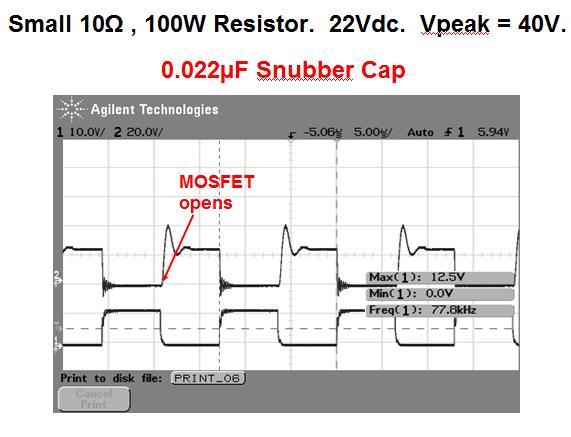
9 10. Before turning on the variac/rransformer/dbr, connect scope leads to simultaneously view VGS and VDS. Initially consider a switching frequency of 100 khz. 11. Set the D control to zero. Raise Vdc (i.e., the DBR voltage) to about 20V. 12. While viewing VGS and VDS, slowly raise D to about 0.5. Observe and measure the peak value and frequency of the ringing overvoltage in VDS. 13. Sweep D over the entire range and verify correct operation. Take simultaneously screen snapshots of PWM output and VGS for 100 khz. 14. If no sign of trouble, repeat the above with the Vdc about 35 to 40V. Take a screen snapshot of VDS. Measure the peak value and frequency of the ringing overvoltage. 15. If no sign of trouble, repeat with 200kHz. 16. Ringing overvoltage is due to the MOSFET capacitance in series with the load circuit s parasitic inductance (including DBR, wires, and resistor). Obviously, in the hard switching case, the ringing overvoltage can be greater than the acceptable twice Vdc. High ringing overvoltage uses up the MOSFET s voltage rating. To reduce ringing overvoltage, slow it down by placing a µf ceramic disk capacitor (a.k,a snubber capacitor ) between the MOSFET s drain and source terminals. Then, repeat the hard switching load test with Vdc, D = 0.5, and re-measure the frequency and peak value of the ringing overvoltage. If removing the snubber capacitor, turn off the DBR first, and then remove the snubber capacitor. Note do not remove or connect the snubber with DBR power applied because the resulting sparks can burn out the MOSFET. Fig. 6. Testing configuration Page 9 of 13


10 17. Duplicate the following conditions and discuss the results. Page 10 of 13

11 Page 11 of 13

12 Page 12 of 13
13 PWM Modulator (On Semiconductor MC34060A) MOSFET Driver, Inverting and Non-Inverting, (MICROCHIP TC1426CPA and TC1427CPA, respectively) Page 13 of 13
H BRIDGE INVERTER. Vdc. Corresponding values of Va and Vb A+ closed, Va = Vdc A closed, Va = 0 B+ closed, Vb = Vdc B closed, Vb = 0 A+ B+ A B
 1. Introduction How do we make AC from DC? Answer the H-Bridge Inverter. H BRIDGE INVERTER Vdc A+ B+ Switching rules Either A+ or A is always closed, but never at the same time * Either B+ or B is always
ECE1750, Spring Week 5 MOSFET Gate Drivers
 ECE1750, Spring 2018 Week 5 MOSFET Gate Drivers 1 Power MOSFETs (a high-speed, voltage-controlled switch) D: Drain D If desired, a series blocking diode can be inserted here to prevent reverse current
i L1 I in Leave the 10µF cap across the input terminals Figure 1. DC-DC SEPIC Converter
 EE46L, Power Electronics, DC-DC SEPIC Converter Version March 1, 01 Overview SEPIC converters make it possible to eiciently convert a DC voltage to either a lower or higher voltage. SEPIC converters are
Lab Experiments. Boost converter (Experiment 2) Control circuit (Experiment 1) Power diode. + V g. C Power MOSFET. Load.
 Control circuit (Experiment 1) Power diode. + V g. C Power MOSFET. Load.") Lab Experiments L Power diode V g C Power MOSFET Load Boost converter (Experiment 2) V ref PWM chip UC3525A Gate driver TSC427 Control circuit (Experiment 1) Adjust duty cycle D The UC3525 PWM Control
Lab Experiments L Power diode V g C Power MOSFET Load Boost converter (Experiment 2) V ref PWM chip UC3525A Gate driver TSC427 Control circuit (Experiment 1) Adjust duty cycle D The UC3525 PWM Control
Assuming continuous conduction, the circuit has two topologies switch closed, and switch open. These are shown in Figures 2a and 2b. L i C.
 EE46, Power Electronics, DC-DC Buck Converter Version Sept. 9, 011 Overview DC-DC converters provide efficient conversion of DC voltage from one level to another. Specifically, the term buck converter
AME140 Lab #2 INTRODUCTION TO ELECTRONIC TEST EQUIPMENT AND BASIC ELECTRONICS MEASUREMENTS
 INTRODUCTION TO ELECTRONIC TEST EQUIPMENT AND BASIC ELECTRONICS MEASUREMENTS The purpose of this document is to guide students through a few simple activities to increase familiarity with basic electronics
University of Utah Electrical & Computer Engineering Department ECE 1250 Lab 4 Pulse Width Modulation Circuit
 University of Utah Electrical & Computer Engineering Department ECE 1250 Lab 4 Pulse Width Modulation Circuit Note: Bring textbook & parts used last time to lab. A. Stolp, 1/8/12 rev, Objective Build a
IR add-on module circuit board assembly - Jeffrey La Favre January 27, 2015
 IR add-on module circuit board assembly - Jeffrey La Favre January 27, 2015 1 2 For the main circuits of the line following robot you soldered electronic components on a printed circuit board (PCB). The
ECE 203 LAB 6: INVERTED PENDULUM
 Version 1.1 1 of 15 BEFORE YOU BEGIN EXPECTED KNOWLEDGE Basic Circuit Analysis EQUIPMENT AFG Oscilloscope Programmable Power Supply MATERIALS Three 741 Opamps TIP41 NPN power transistor TIP42 PNP power
Assembly Instructions
 Assembly Instructions For the SSQ-2F 3.1 MHz Rife Controller Board Kit v1.41 Manual v1.00 2012 by Ralph Hartwell Spectrotek Services GENERAL ASSEMBLY INSTRUCTIONS Arrange for a clean work surface with
ABC V1.0 ASSEMBLY IMPORTANT!
 ABC V1.0 ASSEMBLY Before starting this kit, prepare the following tools: Soldering iron (15-20W will do), flush cutters, no.2 hex screwdriver or allen key and phillips screwdriver. Also briefly go through
Double Pulse Test Board
 Double Pulse Test Board Features 1200 V, 100 A Testing Low Series Inductance Design Wide, 6 oz. Copper Current Traces Multiple DUT and FWD Connections for Long Life Compatible with GeneSiC Gate Drive Mounting
HV739 ±100V 3.0A Ultrasound Pulser Demo Board
 HV79 ±00V.0A Ultrasound Pulser Demo Board HV79DB Introduction The HV79 is a monolithic single channel, high-speed, high voltage, ultrasound transmitter pulser. This integrated, high performance circuit
555 Morse Code Practice Oscillator Kit (draft 1.1)
") This kit was designed to be assembled in about 30 minutes and accomplish the following learning goals: 1. Learn to associate schematic symbols with actual electronic components; 2. Provide a little experience
This kit was designed to be assembled in about 30 minutes and accomplish the following learning goals: 1. Learn to associate schematic symbols with actual electronic components; 2. Provide a little experience
LAB 1 AN EXAMPLE MECHATRONIC SYSTEM: THE FURBY
 LAB 1 AN EXAMPLE MECHATRONIC SYSTEM: THE FURBY Objectives Preparation Tools To see the inner workings of a commercial mechatronic system and to construct a simple manual motor speed controller and current
transformer rectifiers
 Power supply mini-project This week, we finish up 201 lab with a short mini-project. We will build a bipolar power supply and use it to power a simple amplifier circuit. 1. power supply block diagram Figure
LITTLE NERD v1.1 Assembly Guide
 last update: 9. 3. 2016 LITTLE NERD v1.1 Assembly Guide bastl instruments.com INTRODUCTION This guide is for building Little Nerd module from Bastl Instruments. It is good to have basic soldering skills
ELECRAFT Application Note
 ELECRAFT Application Note Front Panel Microphone Circuit Modification Revision A, November 12, 2008 Copyright 2008, Elecraft, Inc., All Rights Reserved Background Some K3 owners have noted distorted transmit
CHAPTER 7 HARDWARE IMPLEMENTATION
 168 CHAPTER 7 HARDWARE IMPLEMENTATION 7.1 OVERVIEW In the previous chapters discussed about the design and simulation of Discrete controller for ZVS Buck, Interleaved Boost, Buck-Boost, Double Frequency
EE362L, Power Electronics, Powering the Grid with Renewable Energy Version Feb. 21, 2009
 Introduction You have successfully built a DC-AC erter. You will now use your erter to convert DC to AC and send power back into the AC. Your access point is a 10 wall outlet. Make sure that your erter
Engineering Design 2 REGULATED POWER SUPPLY PCB PROJECT. Alexander Knapik S Kosta Goulas S Due: Friday
 Engineering Design 2 REGULATED POWER SUPPLY PCB PROJECT Alexander Knapik S3543757 Kosta Goulas S3448324 Due: Friday 14.10.2016 Class: Monday 5:30pm 7:30pm AIM The purpose of this experiment is to design
LA502 Assembly guide Main PCB Resistors - (2)
") LA502 Assembly guide Safety warning The kits are main powered and use potentially lethal voltages. Under no circumstance should someone undertake the realisation of a kit unless he has full knowledge about
LA502 Assembly guide Safety warning The kits are main powered and use potentially lethal voltages. Under no circumstance should someone undertake the realisation of a kit unless he has full knowledge about
Bring your textbook to lab.
 Bring your textbook to lab. Electrical & Computer Engineering Department ECE 2100 Experiment No. 11 Introduction to MOSFET Transistors A. Stolp, 4/3/01 rev,4/6/03 Minimum required points = 46 Recommend
Lecture 4 ECEN 4517/5517
 Lecture 4 ECEN 4517/5517 Experiment 3 weeks 2 and 3: interleaved flyback and feedback loop Battery 12 VDC HVDC: 120-200 VDC DC-DC converter Isolated flyback DC-AC inverter H-bridge v ac AC load 120 Vrms
SoftRock v6.0 Builder s Notes. May 22, 2006
 SoftRock v6.0 Builder s Notes May 22, 2006 Be sure to use a grounded tip soldering iron in building the v6.0 SoftRock circuit board. The soldering iron needs to have a small tip, (0.05-0.1 inch diameter),
EXAMPLE. Use this jack for the red test lead when measuring. current from 0 to 200mA. Figure P-1
 Digital Multimeters ON / OFF power switch Continuity / Diode Test Function Resistance Function Ranges from 200Ω to 200MΩ Transistor Test Function DC Current Function Ranges from 2mA to 20A. AC Current
235 W Maximum Power Dissipation (whole module) 470 T J Junction Operating Temperature -40 to 150. Torque strength
 470 T J Junction Operating Temperature -40 to 150. Torque strength") Discontinued PRODUCT SUMMARY (TYPICAL) V DS (V) 600 R DS(on) (m ) 30 GaN Power Hybrid HEMT Half-Bridge Module Features High frequency operation Free-wheeling diode not required Applications Compact DC-DC
Discontinued PRODUCT SUMMARY (TYPICAL) V DS (V) 600 R DS(on) (m ) 30 GaN Power Hybrid HEMT Half-Bridge Module Features High frequency operation Free-wheeling diode not required Applications Compact DC-DC
Using the isppac-powr1208 MOSFET Driver Outputs
 January 2003 Introduction Using the isppac-powr1208 MOSFET Driver Outputs Application Note AN6043 The isppac -POWR1208 provides a single-chip integrated solution to power supply monitoring and sequencing
The University of Jordan Mechatronics Engineering Department Electronics Lab.( ) Experiment 1: Lab Equipment Familiarization
 Experiment 1: Lab Equipment Familiarization") The University of Jordan Mechatronics Engineering Department Electronics Lab.(0908322) Experiment 1: Lab Equipment Familiarization Objectives To be familiar with the main blocks of the oscilloscope and
The University of Jordan Mechatronics Engineering Department Electronics Lab.(0908322) Experiment 1: Lab Equipment Familiarization Objectives To be familiar with the main blocks of the oscilloscope and
GGD42560 Buck/Boost/Buck-Boost LED Driver
 General Description The GGD42560 is PWM control LED driver with Buck/Boost/Buck-Boost modes, thermal shutdown circuit, current limit circuit, and PWM dimming circuit. Good line regulation and load regulation
SA60. H-Bridge Motor Driver/Amplifiers SA60
 H-Bridge Motor Driver/Amplifiers FEATURES LOW COSOMPLETE H-BRIDGE SELF-CONTAINED SMART LOWSIDE/ HIGHSIDE DRIVE CIRCUITRY WIDE SUPPLY RANGE: UP TO 8V A CONTINUOUS OUTPUT ISOLATED CASE ALLOWS DIRECT HEATSINKING
Ocean Controls KT-5198 Dual Bidirectional DC Motor Speed Controller
 Ocean Controls KT-5198 Dual Bidirectional DC Motor Speed Controller Microcontroller Based Controls 2 DC Motors 0-5V Analog, 1-2mS pulse or Serial Inputs for Motor Speed 10KHz, 1.25KHz or 156Hz selectable
ASTABLE MULTIVIBRATOR
 555 TIMER ASTABLE MULTIIBRATOR MONOSTABLE MULTIIBRATOR 555 TIMER PHYSICS (LAB MANUAL) PHYSICS (LAB MANUAL) 555 TIMER Introduction The 555 timer is an integrated circuit (chip) implementing a variety of
MICROGRANNY v2.1 - Assembly Guide
 last update: 9. 5. 2017 MICROGRANNY v2.1 - Assembly Guide bastl-instruments.com INTRODUCTION Welcome to the assembly guide for the MicroGranny kit. MicroGranny is a monophonic granular sampler by Bastl
High Side MOSFET Gate Drive: The Power of Well. Implemented Pulse Transformers
 High Side MOSFET Gate Drive: The Power of Well Author: Fritz Schlunder SHEF Systems AN-1 Implemented Pulse Transformers Many different techniques and circuits are available for providing high side N-Channel
LED S METER CONSTRUCTION MANUAL. LED S meter Construction Manual Issue 1.0 Page 1
 LED S METER CONSTRUCTION MANUAL LED S meter Construction Manual Issue 1.0 Page 1 Important Please read before starting assembly STATIC PRECAUTION The LED S Meter kit contains components which can be damaged
Application Note 0009
 Recommended External Circuitry for Transphorm GaN FETs Application Note 9 Table of Contents Part I: Introduction... 2 Part II: Solutions to Suppress Oscillation... 2 Part III: The di/dt Limits of GaN Switching
ECE 2010 Laboratory # 5 J.P.O Rourke
 ECE 21 Laboratory # 5 J.P.O Rourke Prelab: Simulate the circuit used in parts 1 and 2 of the Lab and record the simulated results. Your Prelab is due at the beginning of lab and will be checked off by
TS500 Assembly guide. Soldering. TS500 Assembly guide Main PCB 1. Diodes. Document revision 1.2 Last modification : 17/12/16
 TS500 Assembly guide Safety warning The kits are main powered and use potentially lethal voltages. Under no circumstance should someone undertake the realisation of a kit unless he has full knowledge about
University of Jordan School of Engineering Electrical Engineering Department. EE 204 Electrical Engineering Lab
 University of Jordan School of Engineering Electrical Engineering Department EE 204 Electrical Engineering Lab EXPERIMENT 1 MEASUREMENT DEVICES Prepared by: Prof. Mohammed Hawa EXPERIMENT 1 MEASUREMENT
MP6909 Fast Turn-Off Intelligent Rectifier
 MP6909 Fast Turn-Off Intelligent Rectifier The Future of Analog IC Technology DESCRIPTION The MP6909 is a low-drop diode emulator IC that, when combined with an external switch, replaces Schottky diodes
User Manual Rev. 1502
 User Manual Rev. 1502 LDP-AV D06 101/17 / V03 / IF / picolas/manual-ldp-av_d06-n20 PicoLAS GmbH Company for Innovative Power Electronics and Laser Technology Table of Contents LDP-AV D06... 1 Table of
40V, 3A, 500KHz DC/DC Buck Converter
 40V, 3A, 500KHz DC/DC Buck Converter Product Description The is an efficiency and low-cost buck converter with integrated low RDS(ON) high-side 100mΩ MOSFET switch. It is capable of delivering 3A continuous
Double Pulse Switching Board
 Double Pulse Switching Board Features 1200 V, 100 A Testing Low Series Inductance Design Wide, 6 oz. Copper Current Traces Multiple DUT and FWD Connections for Durability Low Resistance and Inductance
MAINTENANCE MANUAL AUDIO MATRIX BOARD P29/
 MAINTENANCE MANUAL AUDIO MATRIX BOARD P29/5000056000 TABLE OF CONTENTS Page DESCRIPTION................................................ Front Cover CIRCUIT ANALYSIS.............................................
SIMULATION WITH THE CUK TOPOLOGY ECE562: Power Electronics I COLORADO STATE UNIVERSITY. Modified in Fall 2011
 SIMULATION WITH THE CUK TOPOLOGY ECE562: Power Electronics I COLORADO STATE UNIVERSITY Modified in Fall 2011 ECE 562 Cuk Converter (NL5 Simulation) Laboratory Page 1 PURPOSE: The purpose of this lab is
EE 230 Lab Lab 9. Prior to Lab
 MOS transistor characteristics This week we look at some MOS transistor characteristics and circuits. Most of the measurements will be done with our usual lab equipment, but we will also use the parameter
V6.2 SoftRock Lite Builder s Notes. November 17, 2006
 V6.2 SoftRock Lite Builder s Notes November 17, 2006 Be sure to use a grounded tip soldering iron in building the v6.2 SoftRock circuit board. The soldering iron needs to have a small tip, (0.05-0.1 inch
Constant Current Switching Regulator for White LED
 Constant Current Switching Regulator for White LED FP7201 General Description The FP7201 is a Boost DC-DC converter specifically designed to drive white LEDs with constant current. The device can support
Chapter 3 : Closed Loop Current Mode DC\DC Boost Converter
 Chapter 3 : Closed Loop Current Mode DC\DC Boost Converter 3.1 Introduction DC/DC Converter efficiently converts unregulated DC voltage to a regulated DC voltage with better efficiency and high power density.
High Speed ±100V 2A Integrated Ultrasound Pulser Demo Board
 Introduction High Speed ±0V A Integrated Ultrasound Pulser Demo Board The HV7 is a complete, high-speed, high voltage, ultrasound tramitter pulser. This integrated high performance circuit is in a single
Features MIC2193BM. Si9803 ( 2) 6.3V ( 2) VDD OUTP COMP OUTN. Si9804 ( 2) Adjustable Output Synchronous Buck Converter
 6.3V ( 2) VDD OUTP COMP OUTN. Si9804 ( 2) Adjustable Output Synchronous Buck Converter") MIC2193 4kHz SO-8 Synchronous Buck Control IC General Description s MIC2193 is a high efficiency, PWM synchronous buck control IC housed in the SO-8 package. Its 2.9V to 14V input voltage range allows
MIC2193 4kHz SO-8 Synchronous Buck Control IC General Description s MIC2193 is a high efficiency, PWM synchronous buck control IC housed in the SO-8 package. Its 2.9V to 14V input voltage range allows
Laboratory Exercises for Analog Circuits and Electronics as Hardware Homework with Student Laptop Computer Instrumentation
 Laboratory Exercises for Analog Circuits and Electronics as Hardware Homework with Student Laptop Computer Instrumentation Marion O. Hagler Department of Electrical and Computer Engineering Mississippi
Features. *Siliconix. Load voltage limited only by MOSFET drain-to-source rating +12V MIC4416 CTL GND. Low-Side Power Switch
 MIC6/7 MIC6/7 IttyBitty Low-Side MOSFET Driver eneral Description The MIC6 and MIC7 IttyBitty low-side MOSFET drivers are designed to switch an N-channel enhancementtype MOSFET from a TTL-compatible control
MIC4414/4415. General Description. Features. Applications. Typical Application. 1.5A, 4.5V to 18V, Low-Side MOSFET Driver
 MIC4414/4415 1.5A, 4.5V to 18V, Low-Side MOSFET Driver General Description The MIC4414 and MIC4415 are low-side MOSFET drivers designed to switch an N-channel enhancement type MOSFET in low-side switch
SPECIFICATION EP 1000/1500/2000 Series
 UNINTERRUPTIBLE POWER SYSTEM SPECIFICATION EP 1000/1500/2000 Series Page 1 of 28 1.0 Revision Summary REVISION SECTION DESCRIPTION Formal Release Page 2 of 28 Table of Contents 1. Introduction. 4 2. Block
EE 3101 ELECTRONICS I LABORATORY EXPERIMENT 7 LAB MANUAL MOSFET AMPLIFIER DESIGN AND ANALYSIS
 EE 3101 ELECTRONICS I LABORATORY EXPERIMENT 7 LAB MANUAL MOSFET AMPLIFIER DESIGN AND ANALYSIS OBJECTIVES In this experiment you will Learn procedures for working with static-sensitive devices. Construct
USER S GUIDE POLOLU A4988 STEPPER MOTOR DRIVER CARRIER USING THE DRIVER POWER CONNECTIONS
 POLOLU A4988 STEPPER MOTOR DRIVER CARRIER USER S GUIDE USING THE DRIVER Minimal wiring diagram for connecting a microcontroller to an A4988 stepper motor driver carrier (full-step mode). POWER CONNECTIONS
Data Conversion and Lab Lab 3 Spring Analog to Digital Converter
 Analog to Digital Converter Lab Report Objectives See separate report form located on the course webpage. This form should be completed during the performance of this lab. 1) To construct and operate an
Introduction to the Op-Amp
 Purpose: ENGR 210/EEAP 240 Lab 5 Introduction to the Op-Amp To become familiar with the operational amplifier (OP AMP), and gain experience using this device in electric circuits. Equipment Required: HP
40106 Hex Oscillator Workshop Instructions. bbob drake, aka fluxmonkey
 40106 Hex Oscillator Workshop Instructions bbob drake, aka fluxmonkey 40106 Hex Oscillator Workshop Instructions by Bbob Drake is licensed under a Creative Commons Attribution-ShareAlike 4.0 International
Introduction. Pictures in this lab have been taken from Pre-Lab Homework
 Introduction This lab relates to material in Hecht, Chapter 18. In this lab you will explore the concepts of circuits, resistors, and capacitors, by actually building a small circuit that is yours to keep!
Bill of Materials: PWM Stepper Motor Driver PART NO
 PWM Stepper Motor Driver PART NO. 2183816 Control a stepper motor using this circuit and a servo PWM signal from an R/C controller, arduino, or microcontroller. Onboard circuitry limits winding current,
Dev Bhoomi Institute Of Technology Department of Electronics and Communication Engineering PRACTICAL INSTRUCTION SHEET
 Dev Bhoomi Institute Of Technology Department of Electronics and Communication Engineering PRACTICAL INSTRUCTION SHEET LABORATORY MANUAL EXPERIMENT NO. ISSUE NO. : ISSUE DATE: REV. NO. : REV. DATE : PAGE:
Read This Page First
 Read This Page First If you are reading this you know the manuals are always available at QRPKITS.com. This is version 8.0 of the manual dated 4/27/2016. There is no need to print out the whole assembly
DC Biased Impedance Measurement
 DC Biased Impedance Measurement Using the Bode 100 and the Picotest J2130A DC Bias Injector By Florian Hämmerle & Steve Sandler 2011 Picotest.com Visit www.picotest.com for more information. Contact support@picotest.com
PowerAmp Design. PowerAmp Design EVAL189 EVALUATION KIT FOR MODEL PAD189. Rev B
 PowerAmp Design EVALUATION KIT FOR MODEL PAD189 Rev B INTRODUCTION The evaluation kit provides a convenient method to become familiar with the operation of amplifier model PAD189 before your application
RT9603. Synchronous-Rectified Buck MOSFET Drivers. General Description. Features. Applications. Ordering Information. Pin Configurations
 Synchronous-Rectified Buck MOSFET Drivers General Description The RT9603 is a high frequency, dual MOSFET drivers specifically designed to drive two power N-MOSFETs in a synchronous-rectified buck converter
ACT111A. 4.8V to 30V Input, 1.5A LED Driver with Dimming Control GENERAL DESCRIPTION FEATURES APPLICATIONS TYPICAL APPLICATION CIRCUIT
 4.8V to 30V Input, 1.5A LED Driver with Dimming Control FEATURES Up to 92% Efficiency Wide 4.8V to 30V Input Voltage Range 100mV Low Feedback Voltage 1.5A High Output Capacity PWM Dimming 10kHz Maximum
PCB layout guidelines. From the IGBT team at IR September 2012
 PCB layout guidelines From the IGBT team at IR September 2012 1 PCB layout and parasitics Parasitics (unwanted L, R, C) have much influence on switching waveforms and losses. The IGBT itself has its own
SoftRock v5.0 Builder s Notes. December 12, Building a QSD Kit
 SoftRock v5.0 Builder s Notes December 12, 2005 Building a QSD Kit Be sure to use a grounded tip soldering iron in building the QSD board. The soldering iron needs to have a small tip, (0.05-0.1 inch diameter),
Recommended External Circuitry for Transphorm GaN FETs. Zan Huang Jason Cuadra
 Recommended External Circuitry for Transphorm GaN FETs Zan Huang Jason Cuadra Application Note Rev. 1.0 November 22, 2016 Table of Contents 1 Introduction 3 2 Sustained oscillation 3 3 Solutions to suppress
TPH3207WS TPH3207WS. GaN Power Low-loss Switch PRODUCT SUMMARY (TYPICAL) Absolute Maximum Ratings (T C =25 C unless otherwise stated)
 Absolute Maximum Ratings (T C =25 C unless otherwise stated)") PRODUCT SUMMARY (TYPICAL) V DS (V) 650 R DS(on) (m ) 35 Q rr (nc) 175 Features Low Q rr Free-wheeling diode not required Quiet Tab for reduced EMI at high dv/dt GSD pin layout improves high speed design
PRODUCT SUMMARY (TYPICAL) V DS (V) 650 R DS(on) (m ) 35 Q rr (nc) 175 Features Low Q rr Free-wheeling diode not required Quiet Tab for reduced EMI at high dv/dt GSD pin layout improves high speed design
ECE 203 LAB 2 CONTROL FUNDAMENTALS AND MAGNETIC LEVITATION
 Version 1.1 1 of 13 ECE 203 LAB 2 CONTROL FUNDAMENTALS AND MAGNETIC LEVITATION BEFORE YOU BEGIN PREREQUISITE LABS All 202 Labs EXPECTED KNOWLEDGE Fundamentals of electrical systems EQUIPMENT Oscilloscope
User Manual LDP-AV D06-N20. máåçi^p=dãäe= `çãé~åó=ñçê=fååçî~íáîé=mçïéê=bäéåíêçåáåë=~åç=i~ëéê=qéåüåçäçöó= = h~áëéêëíê~ëëé=nmm= RONPQ=eÉêòçÖÉåê~íÜ= =
 User Manual LDP-AV D06-N20 máåçi^p=dãäe= `çãé~åó=ñçê=fååçî~íáîé=mçïéê=bäéåíêçåáåë=~åç=i~ëéê=qéåüåçäçöó= = h~áëéêëíê~ëëé=nmm= RONPQ=eÉêòçÖÉåê~íÜ= = müçåéw= HQV=EMF=OQMTJRSP=RUJM= c~ñw= = HQV=EMF=OQMTJRSP=RUJOV=
LM5642 Evaluation Board
 LM5642 Evaluation Board Introduction The LM5642 IC is a dual channel, current-mode, synchronous buck converter controller. It can handle input voltages of up to 36V and delivers two independent output
Experiment (1) Principles of Switching
 Principles of Switching") Experiment (1) Principles of Switching Introduction When you use microcontrollers, sometimes you need to control devices that requires more electrical current than a microcontroller can supply; for this,
Experiment (1) Principles of Switching Introduction When you use microcontrollers, sometimes you need to control devices that requires more electrical current than a microcontroller can supply; for this,
Lab 4: Analysis of the Stereo Amplifier
 ECE 212 Spring 2010 Circuit Analysis II Names: Lab 4: Analysis of the Stereo Amplifier Objectives In this lab exercise you will use the power supply to power the stereo amplifier built in the previous
ML4818 Phase Modulation/Soft Switching Controller
 Phase Modulation/Soft Switching Controller www.fairchildsemi.com Features Full bridge phase modulation zero voltage switching circuit with programmable ZV transition times Constant frequency operation
AN-6203 Applying SG6203 to Control a Synchronous Rectifier of a Flyback Power Supply
 www.fairchildsemi.com AN-6203 Applying SG6203 to Control a Synchronous Rectifier of a Flyback Power Supply Abstract This application note describes a detailed design strategy for a high-efficiency compact
Lab 12: Timing sequencer (Version 1.3)
") Lab 12: Timing sequencer (Version 1.3) WARNING: Use electrical test equipment with care! Always double-check connections before applying power. Look for short circuits, which can quickly destroy expensive
Lab 12: Timing sequencer (Version 1.3) WARNING: Use electrical test equipment with care! Always double-check connections before applying power. Look for short circuits, which can quickly destroy expensive
MIC4421/4422. Bipolar/CMOS/DMOS Process. General Description. Features. Applications. Functional Diagram. 9A-Peak Low-Side MOSFET Driver
 9A-Peak Low-Side MOSFET Driver Micrel Bipolar/CMOS/DMOS Process General Description MIC4421 and MIC4422 MOSFET drivers are rugged, efficient, and easy to use. The MIC4421 is an inverting driver, while
Bi-Directional DC Motor Speed Controller 5-32Vdc (3166v2)
") General Guidelines for Electronic Kits and Assembled Modules Thank you for choosing one of our products. Please take some time to carefully read the important information below concerning use of this product.
General Guidelines for Electronic Kits and Assembled Modules Thank you for choosing one of our products. Please take some time to carefully read the important information below concerning use of this product.
EE283 Electrical Measurement Laboratory Laboratory Exercise #7: Digital Counter
 EE283 Electrical Measurement Laboratory Laboratory Exercise #7: al Counter Objectives: 1. To familiarize students with sequential digital circuits. 2. To show how digital devices can be used for measurement
4.5V to 32V Input High Current LED Driver IC For Buck or Buck-Boost Topology CN5816. Features: SHDN COMP OVP CSP CSN
 4.5V to 32V Input High Current LED Driver IC For Buck or Buck-Boost Topology CN5816 General Description: The CN5816 is a current mode fixed-frequency PWM controller for high current LED applications. The
Hendricks QRP Kits BITX20A to BITX17A Conversion Instructions
 Hendricks QRP Kits BITX20A to BITX17A Conversion Instructions 30 November 2008 Converting your BITX20A Kit to a BITX17A Kit is not all that complex. It only requires that you change crystals and some resonance
12V Dimmer Kit, version 2
 12V Dimmer Kit, version 2 User Manual Description The 12V Dimmer Kit V2 is an especially efficient PWM (pulse-width modulation) controller for 12V loads up to 60 watts. It features a single dial control
TLN-428 Voltage Controlled State Variable Filter
 The Tellun Corporation TLN-428 Voltage Controlled State Variable Filter User Guide, Rev. 1.1 Scott Juskiw The Tellun Corporation scott@tellun.com TLN-428 User Guide Revision 1.1 March 16, 2003 Introduction
Non-Synchronous PWM Boost Controller for LED Driver
 Non-Synchronous PWM Boost Controller for LED Driver General Description The is boost topology switching regulator for LED driver. It provides built-in gate driver pin for driving external N-MOSFET. The
Lab Equipment EECS 311 Fall 2009
 Lab Equipment EECS 311 Fall 2009 Contents Lab Equipment Overview pg. 1 Lab Components.. pg. 4 Probe Compensation... pg. 8 Finite Instrumentation Impedance. pg.10 Simulation Tools..... pg. 10 1 - Laboratory
TFT-LCD DC/DC Converter with Integrated Backlight LED Driver
 TFT-LCD DC/DC Converter with Integrated Backlight LED Driver Description The is a step-up current mode PWM DC/DC converter (Ch-1) built in an internal 1.6A, 0.25Ω power N-channel MOSFET and integrated
10A Current Mode Non-Synchronous PWM Boost Converter
 10A Current Mode Non-Synchronous PWM Boost Converter General Description The is a current mode boost DC-DC converter. It is PWM circuitry with built-in 15mΩ power MOSFET make this regulator highly power
Positive to Negative Buck-Boost Converter Using LM267X SIMPLE SWITCHER Regulators
 Positive to Negative Buck-Boost Converter Using LM267X SIMPLE SWITCHER Regulators Abstract The 3rd generation Simple Switcher LM267X series of regulators are monolithic integrated circuits with an internal
Controlling Input Ripple and Noise in Buck Converters
 Controlling Input Ripple and Noise in Buck Converters Using Basic Filtering Techniques, Designers Can Attenuate These Characteristics and Maximize Performance By Charles Coles, Advanced Analogic Technologies,
Experiment DC-DC converter
 POWER ELECTRONIC LAB Experiment-7-8-9 DC-DC converter Power Electronics Lab Ali Shafique, Ijhar Khan, Dr. Syed Abdul Rahman Kashif 10/11/2015 This manual needs to be completed before the mid-term examination.
AN2170 APPLICATION NOTE MOSFET Device Effects on Phase Node Ringing in VRM Power Converters INTRODUCTION
 AN2170 APPLICATION NOTE MOSFET Device Effects on Phase Node Ringing in VRM Power Converters INTRODUCTION The growth in production volume of industrial equipment (e.g., power DC-DC converters devoted to
Curve Tracer Laboratory Assistant Using the Analog Discovery Module as A Curve Tracer
 Curve Tracer Laboratory Assistant Using the Analog Discovery Module as A Curve Tracer The objective of this lab is to become familiar with methods to measure the dc current-voltage (IV) behavior of diodes
Electronics Fundamentals Courseware
 Innovative Training Solutions Student Lab Manual Electronics Fundamentals Courseware Comprehensive Course in AC / DC Electronics Second Edition Electronics Fundamentals Student Lab Manual Innovative Training
UM1660. Low Power DC/DC Boost Converter UM1660S SOT23-5 UM1660DA DFN AAG PHO. General Description
 General Description Low Power DC/DC Boost Converter S SOT23-5 DA DFN6 2.0 2.0 The is a PFM controlled step-up DC-DC converter with a switching frequency up to 1MHz. The device is ideal to generate output
OCR Electronics for A2 MOSFETs Variable resistors
 Resistance characteristic You are going to find out how the drain-source resistance R d of a MOSFET depends on its gate-source voltage V gs when the drain-source voltage V ds is very small. 1 Assemble