1.2 to 5.5 V TPS79101DBVRQ1(1) PEU1 1.8 V SOT23 TPS79118DBVRQ1(1) PER1 3.3 V (DBV) TPS79133DBVRQ1(1) PES1 4.7 V TPS79147DBVRQ1(1)(2) PET1
|
|
|
- Drusilla Debra Hutchinson
- 5 years ago
- Views:
Transcription
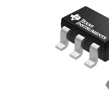
1 SGLS6B APRIL 23 REVISED SEPTEMBER 28 FEATURES Qualified for Automotive Applications ESD Protection Exceeds 2 V Per MIL-STD-883, Method 35; Exceeds 2 V Using Machine Model (C = 2 pf, R = ) -ma Low-Dropout Regulator With EN Available in.8-v, 3.3-V, 4.7-V, and Adj. High PSRR (7 db at khz) Ultralow Noise (5 µv RMS ) Fast Start-Up Time (63 µs) Stable With Any -µf Ceramic Capacitor Excellent Load/Line Transient Very Low Dropout Voltage (38 mv at Full Load, TPS7947) 5-Pin SOT23 (DBV) Package TPS792xx Provides EN Options APPLICATIONS VCOs RF Bluetooth, Wireless LAN DESCRIPTION The TPS79xx family of low-dropout (LDO) low-power linear voltage regulators features high power supply rejection ratio (PSRR), ultralow noise, fast start-up, and excellent line and load transient responses in a small outline, SOT23, package. Each device in the family is stable with a small -µf ceramic capacitor on the output. The family uses an advanced, proprietary BiCMOS fabrication process to yield extremely low dropout voltages (e.g., 38 mv at ma, TPS7947). Each device achieves fast start-up times (approximately 63 µs with a. µf bypass capacitor) while consuming very low quiescent current (7 µa typical). Moreover, when the device is placed in standby mode, the supply current is reduced to less than µa. The exhibits approximately 5 µv RMS of output voltage noise with a. µf bypass capacitor. Applications with analog components that are noise sensitive, such as portable RF electronics, benefit from the high PSRR and low noise features as well as the fast response time. ORDERING INFORMATION TJ VOLTAGE PACKAGE PART NUMBER SYMBOL 4 C to 25 C () The DBVR indicates tape and reel of 3 parts. (2) This part is Product Preview..2 to 5.5 V TPS79DBVRQ() PEU.8 V SOT23 DBVRQ() PER 3.3 V (DBV) DBVRQ() PES 4.7 V TPS7947DBVRQ()(2) PET These devices have limited built-in ESD protection. The leads should be shorted together or the device placed in conductive foam during storage or handling to prevent electrostatic damage to the MOS gates. Please be aware that an important notice concerning availability, standard warranty, and use in critical applications of Texas Instruments semiconductor products and disclaimers thereto appears at the end of this data sheet. Bluetooth is a trademark owned by the Bluetooth SIG, Inc. Copyright 28, Texas Instruments Incorporated
2 SGLS6B APRIL 23 REVISED SEPTEMBER 28 IN GND EN IN GND EN DBV PACKAGE (TOP VIEW) Fixed Option DBV PACKAGE (TOP VIEW) 6 4 OUT BYPASS OUT 5 FB Adjustable Option BYPASS Ripple Rejection db RIPPLE REJECTION Co = µf C(byp) =. µf IO = ma IO = ma 2 k k k M M µv/ Hz Output Spectral Noise Density OUTPUT SPECTRAL NOISE DENSITY IO = ma IO = ma VO = 4.3 V Co = µf C(byp) =. µf k k k ABSOLUTE MAXIMUM RATINGS over operating free-air temperature range unless otherwise noted() 2 Input voltage range(2) Voltage range at EN Voltage on OUT Peak output current ESD rating, HBM ESD rating, CDM Continuous total power dissipation TPS79,, TPS V to 6 V.3 V to VI +.3 V.3 V to 6 V Internally limited 2 kv 5 V See Dissipation Rating Table Operating virtual junction temperature range, TJ 4 C to 5 C Operating ambient temperature range, TA 4 C to 85 C Storage temperature range, Tstg 65 C to 5 C () Stresses beyond those listed under absolute maximum ratings may cause permanent damage to the device. These are stress ratings only, and functional operation of the device at these or any other conditions beyond those indicated under recommended operating conditions is not implied. Exposure to absolute-maximum-rated conditions for extended periods may affect device reliability. (2) All voltage values are with respect to network ground terminal. PACKAGE DISSIPATION RATING BOARD PACKAGE RθJC RθJA DERATING FACTOR ABOVE TA = 25 C TA 25 C POWER RATING TA = 7 C POWER RATING TA = 85 C POWER RATING Low K() DBV C/W 256 C/W 3.96 mw/ C 39 mw 25 mw 56 mw High K(2) DBV C/W 78.3 C/W 5.69 mw/ C 56 mw 38 mw 224 mw () The JEDEC low-k (s) board design used to derive this data was a 3-inch 3-inch, two-layer board with 2-ounce copper traces on top of the board. (2) The JEDEC high-k (2s2p) board design used to derive this data was a 3-inch 3-inch, multilayer board with -ounce internal power and ground planes and 2-ounce copper traces on top and bottom of the board. RECOMMENDED OPERATING CONDITIONS MIN NOM MAX UNIT Input voltage, VI () V Continuous output current, IO (2) ma Operating junction temperature, TJ 4 25 C () To calculate the minimum input voltage for your maximum output current, use the following formula: VI(min) = VO(max) + VDO (max load) (2) Continuous output current and operating junction temperature are limited by internal protection circuitry, but it is not recommended that the device operate under conditions beyond those specified in this table for extended periods of time.
3 SGLS6B APRIL 23 REVISED SEPTEMBER 28 ELECTRICAL CHARACTERISTICS over recommended operating free-air temperature range, (TJ = 4 to 25 C), VI = VO(typ) + V, IO = ma, EN = V, Co = µf, Co(byp)=. µf (unless otherwise noted) Output voltage Quiescent current (GND current) PARAMETER TEST CONDITIONS MIN TYP MAX UNIT TJ = 25 C,.22 V VO 5.2 V VO TPS79 TPS7947 µa< IO < ma(),.22 V VO 5.2 V.98 VO.2 VO TJ = 25 C.8 µa < IO < ma, 2.8 V < VI < 5.5 V V TJ = 25 C 3.3 µa < IO < ma, 4.3 V < VI < 5.5 V TJ = 25 C 4.7 µa < IO < ma, 5.2 V < VI < 5.5 V µa < IO < ma, TJ = 25 C 7 µa < IO < ma 25 Load regulation µa < IO < ma, TJ = 25 C 5 mv Output voltage line regulation ( VO/VO)(2) Output noise voltage () Time, start-up () VO + V < VI 5.5 V, TJ = 25 C.5 VO + V < VI 5.5 V.2 C(byp) =. µf 32 BW = Hz to khz, C(byp) =.47 µf 7 IO = ma, TJ = 25 C C(byp) =. µf 6 RL = 33 Ω,, Co = µf, TJ = 25 C C(byp) =. µf 5 C(byp) =. µf 53 µaa %/V µvrmsv C(byp) =.47 µf 67 µs C(byp) =. µf 98 Output current limit VO = V() ma UVLO threshold VCC rising V UVLO hysteresis TJ = 25 C, VCC rising mv () The minimum IN operating voltage is 2.7 V or VO(typ) + V, whichever is greater. The maximum IN voltage is 5.5 V. The maximum output current is ma. (2) If VO.8 V then VImin = 2.7 V, VImax = 5.5 V: V V 2.7 Line regulation (mv) % V O Imax V If VO 2.5 V then VImin = VO + V, VImax = 5.5 V: V O V Imax V O V Line regulation (mv) % V 3
4 SGLS6B APRIL 23 REVISED SEPTEMBER 28 ELECTRICAL CHARACTERISTICS continued over recommended operating free-air temperature range, (TJ = 4 to 25 C), VI = VO(typ) + V, IO = ma, EN = V, Co = µf, Co(byp)=. µf (unless otherwise noted) PARAMETER TEST CONDITIONS MIN TYP MAX UNIT Standby current EN = VI, 2.7 V < VI < 5.5 V.7 µa High level enable input voltage 2.7 V < VI < 5.5 V 2 V Low level enable input voltage 2.7 V < VI < 5.5 V.7 V Input current (EN) EN = VI µa Power supply ripple rejection f = Hz, TJ = 25 C, IO = ma 8 f = Hz, TJ = 25 C, IO = ma 75 f = khz, TJ = 25 C, IO = ma 72 f = khz, TJ = 25 C, IO = ma 45 f = Hz, TJ = 25 C, IO = ma 7 f = Hz, TJ = 25 C, IO = ma 75 f = khz, TJ = 25 C, IO = ma 73 f = khz, TJ = 25 C, IO = ma 37 IO = ma, TJ = 25 C 5 IO = ma 9 Dropout voltage() IO = ma, TJ = 25 C 38 TPS7947 IO = ma 7 () IN voltage equals VO(typ) mv; The dropout voltage is limited by the input voltage range limitations. db mv 4
5 SGLS6B APRIL 23 REVISED SEPTEMBER 28 FUNCTIONAL BLOCK DIAGRAM ADJUSTABLE VERSION VIN VOUT GND UVLO Current Sense ILIM _ + SHUTDOWN R FB EN UVLO R2 Thermal Shutdown External to the Device VIN Bandgap Reference 25 kω Vref Bypass FUNCTIONAL BLOCK DIAGRAM FIXED VERSION VIN VOUT GND EN UVLO Current Sense ILIM _ + SHUTDOWN R Thermal Shutdown UVLO R2 VIN Bandgap Reference 25 kω Vref Bypass Terminal Functions TERMINAL NAME ADJ FIXED I/O DESCRIPTION BYPASS 4 4 An external bypass capacitor, connected to this terminal, in conjunction with an internal resistor, creates a low-pass filter to further reduce regulator noise. EN 3 3 I The EN terminal is an input which enables or shuts down the device. When EN is a logic high, the device will be in shutdown mode. When EN is a logic low, the device will be enabled. FB 5 N/A I This terminal is the feedback input voltage for the adjustable device. GND 2 2 Regulator ground IN I The IN terminal is the input to the device. OUT 6 5 O The OUT terminal is the regulated output of the device. 5
6 SGLS6B APRIL 23 REVISED SEPTEMBER 28 TYPICAL CHARACTERISTICS V O Output Voltage V OUTPUT VOLTAGE OUTPUT CURRENT VI = 2.8 V Co = µf TJ = 25 C V O Output Voltage V OUTPUT VOLTAGE OUTPUT CURRENT Co = µf TJ = 25 C V O Output Voltage V OUTPUT VOLTAGE JUNCTION TEMPERATURE VI = 2.8 V Co = µf IO = ma IO = ma IO Output Current ma Figure IO Output Current ma Figure TJ Junction Temperature C Figure 3 Output Voltage V V O OUTPUT VOLTAGE JUNCTION TEMPERATURE Co = µf IO = ma TJ Junction Temperature C Figure 4 IO = ma Ground Current µ A GROUND CURRENT JUNCTION TEMPERATURE Co = µf IO = ma TJ Junction Temperature C Figure 5 IO = ma µv/ Hz Output Spectral Noise Density OUTPUT SPECTRAL NOISE DENSITY IO = ma IO = ma VI = 2.8 V Co = µf C(byp) =. µf k k k Figure 6 µv/ Hz Output Spectral Noise Density OUTPUT SPECTRAL NOISE DENSITY IO = ma IO = ma VI = 2.8 V Co = µf C(byp) =. µf k k k Figure 7 Output Spectral Noise Density µ V/ Hz OUTPUT SPECTRAL NOISE DENSITY.2 IO =. µf VI = 2.8 V IO = ma Co = µf IO =.47 µf IO =. µf IO =. µf k k k Figure 8 µv/ Hz Output Spectral Noise Density OUTPUT SPECTRAL NOISE DENSITY IO = ma IO = ma Co = µf C(byp) =. µf k k k Figure 9 6
7 SGLS6B APRIL 23 REVISED SEPTEMBER 28 TYPICAL CHARACTERISTICS µv/ Hz Output Spectral Noise Density OUTPUT SPECTRAL NOISE DENSITY IO = ma IO = ma Co = µf C(byp) =. µf k k k Figure Output Spectral Noise Density µ V/ Hz OUTPUT SPECTRAL NOISE DENSITY 2.8 IO =. µf IO = ma.6 Co = µf IO =.47 µf IO =. µf IO =. µf k k k Figure V (RMS) µ RMS Root Mean Squared Output Noise ROOT MEAN SQUARED OUTPUT NOISE BYPASS CAPACITANCE 7 BW = Hz to 6 khz VO = 3.3 V VO =.8 V... C(bypass) Bypass Capacitance µf Figure 2 Z o Output Impedance Ω OUTPUT IMPEDANCE Co = µf TJ = 25 C IO = ma IO = ma k k k M M Figure 3 Dropout Voltage mv V DO DROPOUT VOLTAGE JUNCTION TEMPERATURE VI = 3.2 V, Co = µf TJ Junction Temperature C Figure 4 IO = ma IO = ma V DO Dropout Voltage mv TPS79233 DROPOUT VOLTAGE OUTPUT CURRENT VI = 3.2 V CO = µf TJ = 25 C IO Output Current A Figure 5 TJ = 25 C TJ = 4 C V DO Dropout Voltage mv TPS79 DROPOUT VOLTAGE INPUT VOLTAGE Figure 6 TJ = 25 C TJ = 25 C TJ = 4 C VI Input Voltage V IO = ma Minimum Required Input Voltage V MINIMUM REQUIRED INPUT VOLTAGE OUTPUT VOLTAGE VI = 3.2 V Co = µf TJ = 4 C TJ = 25 C TJ = 25 C VO Output Voltage V Figure 7 Ripple Rejection db RIPPLE REJECTION IO = ma IO = ma 2 VI = 2.8 V Co = µf C(byp) =. µf k k k M M Figure 8 7
8 SGLS6B APRIL 23 REVISED SEPTEMBER 28 TYPICAL CHARACTERISTICS Ripple Rejection db RIPPLE REJECTION IO = ma IO = ma 2 VI = 2.8 V Co = µf C(byp) =. µf k k k M M Figure 9 Ripple Rejection db RIPPLE REJECTION IO = ma IO = ma 2 VI = 2.8 V Co = µf C(byp) =. µf k k k M M Figure 2 Ripple Rejection db RIPPLE REJECTION Co = µf C(byp) =. µf IO = ma IO = ma 2 k k k M M Figure 2 Ripple Rejection db RIPPLE REJECTION CO = µf C(byp) =. µf IO = ma 2 k k k M M Figure 22 IO = ma Ripple Rejection db RIPPLE REJECTION Co = µf C(byp) =. µf IO = ma Figure 23 IO = ma 2 k k k M M OUTPUT VOLTAGE, ENABLE VOLTAGE TIME (START-UP) 3 2 VO = 3.3 V IO = ma Co = µf TJ = 25 C Enable Voltage V Output Voltage V V O 3 2 C(byp) =. µf t Time µs Figure 24 C(byp) =.47 µf C(byp) =. µf V O Output Voltage mv V I Input Voltage V 3.8 LINE TRANSIENT RESPONSE IO = ma Co = µf C(byp) =. µf t Time µs Figure 25 V Change In O Output Voltage mv Current Load ma LOAD TRANSIENT RESPONSE k 2 k 4 k 6 k 8 k 2 k t Time µs Figure 26 VI = 2.8 V Co = µf Output Voltage mv V O V I Input Voltage V LINE TRANSIENT RESPONSE IO = ma Co = µf C(byp) =. µf t Time µs Figure 27 dv.4 V dt µs 8
9 V Change In O Output Voltage mv I O Output Current ma LOAD TRANSIENT RESPONSE t Time µs Figure 28 Co = µf TYPICAL CHARACTERISTICS ESR Equivalent Series Resistance Ω. SGLS6B APRIL 23 REVISED SEPTEMBER 28 TYPICAL REGIONS OF STABILITY EQUIVALENT SERIES RESISTANCE (ESR) OUTPUT CURRENT Co =.47 µf VI = 5.5 V TJ = 4 C to 25 C Region of Instability Region of Instability IO Output Current A Figure 29 ESR Equivalent Series Resistance Ω TYPICAL REGIONS OF STABILITY EQUIVALENT SERIES RESISTANCE (ESR) OUTPUT CURRENT Co = µf VI = 5.5 V TJ = 4 C to 25 C Region of Instability. Region of Stability IO Output Current A Figure 3 ESR Equivalent Series Resistance Ω TYPICAL REGIONS OF STABILITY EQUIVALENT SERIES RESISTANCE (ESR) OUTPUT CURRENT. Co = µf VI = 5.5 V TJ = 4 C to 25 C Region of Instability Region of Stability IO Output Current A Figure 3 9
10 SGLS6B APRIL 23 REVISED SEPTEMBER 28 APPLICATION INFORMATION The TPS79xx family of low-dropout (LDO) regulators have been optimized for use in noise-sensitive battery-operated equipment. The device features extremely low dropout voltages, high PSRR, ultralow output noise, low quiescent current (7 µa typically), and enable-input to reduce supply currents to less than µa when the regulator is turned off. A typical application circuit is shown in Figure 32. TPS79xx VI IN BYPASS 4. µf 3 OUT EN GND 2 5 VO + µf. µf EXTERNAL CAPACITOR REQUIREMENTS Figure 32. Typical Application Circuit A.-µF or larger ceramic input bypass capacitor, connected between IN and GND and located close to the TPS79xx, is required for stability and to improve transient response, noise rejection, and ripple rejection. A higher-value electrolytic input capacitor may be necessary if large, fast-rise-time load transients are anticipated and the device is located several inches from the power source. Like all low dropout regulators, the TPS79xx requires an output capacitor connected between OUT and GND to stabilize the internal control loop. The minimum recommended capacitance is µf. Any µf or larger ceramic capacitor is suitable. The device is also stable with a.47 µf ceramic capacitor with at least 75 mω of ESR. The internal voltage reference is a key source of noise in an LDO regulator. The TPS79xx has a BYPASS pin which is connected to the voltage reference through a 25-kΩ internal resistor. The 25-kΩ internal resistor, in conjunction with an external bypass capacitor connected to the BYPASS pin, creates a low pass filter to reduce the voltage reference noise and, therefore, the noise at the regulator output. In order for the regulator to operate properly, the current flow out of the BYPASS pin must be at a minimum because any leakage current creates an IR drop across the internal resistor thus creating an output error. Therefore, the bypass capacitor must have minimal leakage current. For example, the exhibits approximately 5 µv RMS of output voltage noise using a. µf ceramic bypass capacitor and a µf ceramic output capacitor. Note that the output starts up slower as the bypass capacitance increases due to the RC time constant at the bypass pin that is created by the internal 25 kω resistor and external capacitor. BOARD LAYOUT RECOMMENDATION TO IMPROVE PSRR AND NOISE PERFORMANCE To improve ac measurements like PSRR, output noise, and transient response, it is recommended that the board be designed with separate ground planes for V IN and V OUT, with each ground plane connected only at the ground pin of the device. In addition, the ground connection for the bypass capacitor should connect directly to the ground pin of the device.
11 SGLS6B APRIL 23 REVISED SEPTEMBER 28 POWER DISSIPATION AND JUNCTION TEMPERATURE Specified regulator operation is assured to a junction temperature of 25 C; the maximum junction temperature should be restricted to 25 C under normal operating conditions. This restriction limits the power dissipation the regulator can handle in any given application. To ensure the junction temperature is within acceptable limits, calculate the maximum allowable dissipation, P D(max), and the actual dissipation, P D, which must be less than or equal to P D(max). The maximum-power-dissipation limit is determined using the following equation: P D(max) T J max T A R JA () Where: T J max is the maximum allowable junction temperature. R θja is the thermal resistance junction-to-ambient for the package, see the dissipation rating table. T A is the ambient temperature. The regulator dissipation is calculated using: P D V I V O I O (2) Power dissipation resulting from quiescent current is negligible. Excessive power dissipation triggers the thermal protection circuit. PROGRAMMING THE TPS79 ADJUSTABLE LDO REGULATOR The output voltage of the TPS79 adjustable regulator is programmed using an external resistor divider as shown in Figure 33. The output voltage is calculated using: V V R O ref R2 (3) Where: V ref =.2246 V typ (the internal reference voltage) Resistors R and R2 should be chosen for approximately 5-µA divider current. Lower value resistors can be used for improved noise performance, but the solution consumes more power. Higher resistor values should be avoided as leakage current into/out of FB across R/R2 creates an offset voltage that artificially increases/decreases the feedback voltage and thus erroneously decreases/increases V O. The recommended design procedure is to choose R2 = 3. kω to set the divider current at 5 µa, C = 5 pf for stability, and then calculate R using: R V O V ref R2 (4) In order to improve the stability of the adjustable version, it is suggested that a small compensation capacitor be placed between OUT and FB. For voltages <.8 V, the value of this capacitor should be pf. For voltages >.8 V, the approximate value of this capacitor can be calculated as: C (3 7 ) (R R2) (5) (R R2) The suggested value of this capacitor for several resistor ratios is shown in the table below. If this capacitor is not used (such as in a unity-gain configuration) or if an output voltage <.8 V is chosen, then the minimum recommended output capacitor is 2.2 µf instead of µf.
12 SGLS6B APRIL 23 REVISED SEPTEMBER 28.7 V VI µf 2 V. µf TPS79 IN EN OUT BYPASS FB GND C R R2 VO µf OUTPUT VOLTAGE 2.5 V 3.3 V 3.6 V OUTPUT VOLTAGE PROGRAMMING GUIDE R 3.6 kω 5 kω 59 kω R2 3. kω 3. kω 3. kω C 22 pf 5 pf 5 pf REGULATOR PROTECTION Figure 33. TPS79 Adjustable LDO Regulator Programming The TPS79xx PMOS-pass transistor has a built-in back diode that conducts reverse current when the input voltage drops below the output voltage (e.g., during power down). Current is conducted from the output to the input and is not internally limited. If extended reverse voltage operation is anticipated, external limiting might be appropriate. The TPS79xx features internal current limiting and thermal protection. During normal operation, the TPS79xx limits output current to approximately 4 ma. When current limiting engages, the output voltage scales back linearly until the overcurrent condition ends. While current limiting is designed to prevent gross device failure, care should be taken not to exceed the power dissipation ratings of the package or the absolute maximum voltage ratings of the device. If the temperature of the device exceeds approximately 65 C, thermal-protection circuitry shuts it down. Once the device has cooled down to below approximately 4 C, regulator operation resumes. 2
13 PACKAGE OPTION ADDENDUM 7-Mar-27 PACKAGING INFORMATION Orderable Device Status () Package Type Package Drawing Pins Package Qty Eco Plan TPS79DBVRQ ACTIVE SOT-23 DBV 6 3 Green (RoHS & no Sb/Br) DBVRQ ACTIVE SOT-23 DBV 5 3 Green (RoHS & no Sb/Br) (2) Lead/Ball Finish (6) MSL Peak Temp (3) Op Temp ( C) Device Marking (4/5) CU NIPDAU Level--26C-UNLIM -4 to 25 PEU CU NIPDAU Level--26C-UNLIM -4 to 25 PER Samples () The marketing status values are defined as follows: ACTIVE: Product device recommended for new designs. LIFEBUY: TI has announced that the device will be discontinued, and a lifetime-buy period is in effect. NRND: Not recommended for new designs. Device is in production to support existing customers, but TI does not recommend using this part in a new design. PREVIEW: Device has been announced but is not in production. Samples may or may not be available. OBSOLETE: TI has discontinued the production of the device. (2) Eco Plan - The planned eco-friendly classification: Pb-Free (RoHS), Pb-Free (RoHS Exempt), or Green (RoHS & no Sb/Br) - please check for the latest availability information and additional product content details. TBD: The Pb-Free/Green conversion plan has not been defined. Pb-Free (RoHS): TI's terms "Lead-Free" or "Pb-Free" mean semiconductor products that are compatible with the current RoHS requirements for all 6 substances, including the requirement that lead not exceed.% by weight in homogeneous materials. Where designed to be soldered at high temperatures, TI Pb-Free products are suitable for use in specified lead-free processes. Pb-Free (RoHS Exempt): This component has a RoHS exemption for either ) lead-based flip-chip solder bumps used between the die and package, or 2) lead-based die adhesive used between the die and leadframe. The component is otherwise considered Pb-Free (RoHS compatible) as defined above. Green (RoHS & no Sb/Br): TI defines "Green" to mean Pb-Free (RoHS compatible), and free of Bromine (Br) and Antimony (Sb) based flame retardants (Br or Sb do not exceed.% by weight in homogeneous material) (3) MSL, Peak Temp. - The Moisture Sensitivity Level rating according to the JEDEC industry standard classifications, and peak solder temperature. (4) There may be additional marking, which relates to the logo, the lot trace code information, or the environmental category on the device. (5) Multiple Device Markings will be inside parentheses. Only one Device Marking contained in parentheses and separated by a "~" will appear on a device. If a line is indented then it is a continuation of the previous line and the two combined represent the entire Device Marking for that device. (6) Lead/Ball Finish - Orderable Devices may have multiple material finish options. Finish options are separated by a vertical ruled line. Lead/Ball Finish values may wrap to two lines if the finish value exceeds the maximum column width. Important Information and Disclaimer:The information provided on this page represents TI's knowledge and belief as of the date that it is provided. TI bases its knowledge and belief on information provided by third parties, and makes no representation or warranty as to the accuracy of such information. Efforts are underway to better integrate information from third parties. TI has taken and continues to take reasonable steps to provide representative and accurate information but may not have conducted destructive testing or chemical analysis on incoming materials and chemicals. TI and TI suppliers consider certain information to be proprietary, and thus CAS numbers and other limited information may not be available for release. Addendum-Page
14 PACKAGE OPTION ADDENDUM 7-Mar-27 In no event shall TI's liability arising out of such information exceed the total purchase price of the TI part(s) at issue in this document sold by TI to Customer on an annual basis. OTHER QUALIFIED VERSIONS OF TPS79-Q : Catalog: TPS79 NOTE: Qualified Version Definitions: Catalog - TI's standard catalog product Addendum-Page 2
15 PACKAGE MATERIALS INFORMATION 27-Apr-26 TAPE AND REEL INFORMATION *All dimensions are nominal Device Package Type Package Drawing Pins SPQ Reel Diameter (mm) Reel Width W (mm) A (mm) B (mm) K (mm) P (mm) W (mm) Pin Quadrant TPS79DBVRQ SOT-23 DBV Q3 DBVRQ SOT-23 DBV Q3 Pack Materials-Page
16 PACKAGE MATERIALS INFORMATION 27-Apr-26 *All dimensions are nominal Device Package Type Package Drawing Pins SPQ Length (mm) Width (mm) Height (mm) TPS79DBVRQ SOT-23 DBV DBVRQ SOT-23 DBV Pack Materials-Page 2
17
18

19
20 SCALE 4. PACKAGE OUTLINE DBV5A SOT mm max height SMALL OUTLINE TRANSISTOR C C PIN INDEX AREA B A.45 MAX 5.9 2X X C A B 4 (.).5 TYP..25 GAGE PLANE.22 TYP.8 8 TYP.6 TYP.3 SEATING PLANE /C 4/27 NOTES:. All linear dimensions are in millimeters. Any dimensions in parenthesis are for reference only. Dimensioning and tolerancing per ASME Y4.5M. 2. This drawing is subject to change without notice. 3. Refernce JEDEC MO-78.
21 DBV5A EXAMPLE BOARD LAYOUT SOT mm max height SMALL OUTLINE TRANSISTOR 5X (.) PKG 5X (.6) 5 2 SYMM (.9) 2X (.95) 3 4 (R.5) TYP (2.6) LAND PATTERN EXAMPLE EXPOSED METAL SHOWN SCALE:5X SOLDER MASK OPENING METAL METAL UNDER SOLDER MASK SOLDER MASK OPENING EXPOSED METAL EXPOSED METAL.7 MAX ARROUND NON SOLDER MASK DEFINED (PREFERRED).7 MIN ARROUND SOLDER MASK DEFINED SOLDER MASK DETAILS /C 4/27 NOTES: (continued) 4. Publication IPC-735 may have alternate designs. 5. Solder mask tolerances between and around signal pads can vary based on board fabrication site.
22 DBV5A EXAMPLE STENCIL DESIGN SOT mm max height SMALL OUTLINE TRANSISTOR 5X (.6) 5X (.) PKG 5 2X(.95) 2 SYMM (.9) 3 4 (R.5) TYP (2.6) SOLDER PASTE EXAMPLE BASED ON.25 mm THICK STENCIL SCALE:5X /C 4/27 NOTES: (continued) 6. Laser cutting apertures with trapezoidal walls and rounded corners may offer better paste release. IPC-7525 may have alternate design recommendations. 7. Board assembly site may have different recommendations for stencil design.
23 IMPORTANT NOTICE Texas Instruments Incorporated (TI) reserves the right to make corrections, enhancements, improvements and other changes to its semiconductor products and services per JESD46, latest issue, and to discontinue any product or service per JESD48, latest issue. Buyers should obtain the latest relevant information before placing orders and should verify that such information is current and complete. TI s published terms of sale for semiconductor products ( apply to the sale of packaged integrated circuit products that TI has qualified and released to market. Additional terms may apply to the use or sale of other types of TI products and services. Reproduction of significant portions of TI information in TI data sheets is permissible only if reproduction is without alteration and is accompanied by all associated warranties, conditions, limitations, and notices. TI is not responsible or liable for such reproduced documentation. Information of third parties may be subject to additional restrictions. Resale of TI products or services with statements different from or beyond the parameters stated by TI for that product or service voids all express and any implied warranties for the associated TI product or service and is an unfair and deceptive business practice. TI is not responsible or liable for any such statements. Buyers and others who are developing systems that incorporate TI products (collectively, Designers ) understand and agree that Designers remain responsible for using their independent analysis, evaluation and judgment in designing their applications and that Designers have full and exclusive responsibility to assure the safety of Designers' applications and compliance of their applications (and of all TI products used in or for Designers applications) with all applicable regulations, laws and other applicable requirements. Designer represents that, with respect to their applications, Designer has all the necessary expertise to create and implement safeguards that () anticipate dangerous consequences of failures, (2) monitor failures and their consequences, and (3) lessen the likelihood of failures that might cause harm and take appropriate actions. Designer agrees that prior to using or distributing any applications that include TI products, Designer will thoroughly test such applications and the functionality of such TI products as used in such applications. TI s provision of technical, application or other design advice, quality characterization, reliability data or other services or information, including, but not limited to, reference designs and materials relating to evaluation modules, (collectively, TI Resources ) are intended to assist designers who are developing applications that incorporate TI products; by downloading, accessing or using TI Resources in any way, Designer (individually or, if Designer is acting on behalf of a company, Designer s company) agrees to use any particular TI Resource solely for this purpose and subject to the terms of this Notice. TI s provision of TI Resources does not expand or otherwise alter TI s applicable published warranties or warranty disclaimers for TI products, and no additional obligations or liabilities arise from TI providing such TI Resources. TI reserves the right to make corrections, enhancements, improvements and other changes to its TI Resources. TI has not conducted any testing other than that specifically described in the published documentation for a particular TI Resource. Designer is authorized to use, copy and modify any individual TI Resource only in connection with the development of applications that include the TI product(s) identified in such TI Resource. NO OTHER LICENSE, EXPRESS OR IMPLIED, BY ESTOPPEL OR OTHERWISE TO ANY OTHER TI INTELLECTUAL PROPERTY RIGHT, AND NO LICENSE TO ANY TECHNOLOGY OR INTELLECTUAL PROPERTY RIGHT OF TI OR ANY THIRD PARTY IS GRANTED HEREIN, including but not limited to any patent right, copyright, mask work right, or other intellectual property right relating to any combination, machine, or process in which TI products or services are used. Information regarding or referencing third-party products or services does not constitute a license to use such products or services, or a warranty or endorsement thereof. Use of TI Resources may require a license from a third party under the patents or other intellectual property of the third party, or a license from TI under the patents or other intellectual property of TI. TI RESOURCES ARE PROVIDED AS IS AND WITH ALL FAULTS. TI DISCLAIMS ALL OTHER WARRANTIES OR REPRESENTATIONS, EXPRESS OR IMPLIED, REGARDING RESOURCES OR USE THEREOF, INCLUDING BUT NOT LIMITED TO ACCURACY OR COMPLETENESS, TITLE, ANY EPIDEMIC FAILURE WARRANTY AND ANY IMPLIED WARRANTIES OF MERCHANTABILITY, FITNESS FOR A PARTICULAR PURPOSE, AND NON-INFRINGEMENT OF ANY THIRD PARTY INTELLECTUAL PROPERTY RIGHTS. TI SHALL NOT BE LIABLE FOR AND SHALL NOT DEFEND OR INDEMNIFY DESIGNER AGAINST ANY CLAIM, INCLUDING BUT NOT LIMITED TO ANY INFRINGEMENT CLAIM THAT RELATES TO OR IS BASED ON ANY COMBINATION OF PRODUCTS EVEN IF DESCRIBED IN TI RESOURCES OR OTHERWISE. IN NO EVENT SHALL TI BE LIABLE FOR ANY ACTUAL, DIRECT, SPECIAL, COLLATERAL, INDIRECT, PUNITIVE, INCIDENTAL, CONSEQUENTIAL OR EXEMPLARY DAMAGES IN CONNECTION WITH OR ARISING OUT OF TI RESOURCES OR USE THEREOF, AND REGARDLESS OF WHETHER TI HAS BEEN ADVISED OF THE POSSIBILITY OF SUCH DAMAGES. Unless TI has explicitly designated an individual product as meeting the requirements of a particular industry standard (e.g., ISO/TS 6949 and ISO 26262), TI is not responsible for any failure to meet such industry standard requirements. Where TI specifically promotes products as facilitating functional safety or as compliant with industry functional safety standards, such products are intended to help enable customers to design and create their own applications that meet applicable functional safety standards and requirements. Using products in an application does not by itself establish any safety features in the application. Designers must ensure compliance with safety-related requirements and standards applicable to their applications. Designer may not use any TI products in life-critical medical equipment unless authorized officers of the parties have executed a special contract specifically governing such use. Life-critical medical equipment is medical equipment where failure of such equipment would cause serious bodily injury or death (e.g., life support, pacemakers, defibrillators, heart pumps, neurostimulators, and implantables). Such equipment includes, without limitation, all medical devices identified by the U.S. Food and Drug Administration as Class III devices and equivalent classifications outside the U.S. TI may expressly designate certain products as completing a particular qualification (e.g., Q, Military Grade, or Enhanced Product). Designers agree that it has the necessary expertise to select the product with the appropriate qualification designation for their applications and that proper product selection is at Designers own risk. Designers are solely responsible for compliance with all legal and regulatory requirements in connection with such selection. Designer will fully indemnify TI and its representatives against any damages, costs, losses, and/or liabilities arising out of Designer s noncompliance with the terms and provisions of this Notice. Mailing Address: Texas Instruments, Post Office Box 65533, Dallas, Texas Copyright 28, Texas Instruments Incorporated
150-mA LOW-NOISE LDO WITH IN-RUSH CURRENT CONTROL FOR USB APPLICATION
 TPS7882, TPS78833 -ma LOW-NOISE LDO WITH IN-RUSH CURRENT CONTROL FOR USB APPLICATION SLVS382A JUNE 2 REVISED JULY 2 FEATURES -ma Low-Dropout Regulator Available in 2. V, 3.3 V Programmable Slew Rate Control
description/ordering information
 µ SLVS060K JUNE 1976 REVISED APRIL 2005 3-Terminal Regulators Output Current Up To 500 ma No External Components High Power-Dissipation Capability Internal Short-Circuit Current Limiting Output Transistor
GENERAL-PURPOSE LOW-VOLTAGE COMPARATORS
 1 LMV331-Q1 SINGLE, LMV393-Q1 DUAL SLOS468D MAY 2005 REVISED AUGUST 2011 GENERAL-PURPOSE LOW-VOLTAGE COMPARATORS Check for Samples: LMV331-Q1 SINGLE, LMV393-Q1 DUAL 1FEATURES Qualified for Automotive Applications
TPS76130, TPS76132, TPS76133, TPS76138, TPS76150 LOW-POWER 100-mA LOW-DROPOUT LINEAR REGULATORS
 TPS76130, TPS76132, TPS76133, TPS76138, TPS7610 LOW-POWER 100-mA LOW-DROPOUT LINEAR REGULATORS SLVS178B DECEMBER 1998 REVISED MAY 2001 100-mA Low-Dropout Regulator Fixed Output Voltage Options: V, 3.8
Data sheet acquired from Harris Semiconductor SCHS083B Revised March 2003
 Data sheet acquired from Harris Semiconductor SCHS083B Revised March 2003 The CD4536B types are supplied in 16-lead hermetic dual-in-line ceramic packages (F3A suffix), 16-lead dual-in-line plastic packages
LOW INPUT VOLTAGE, CAP FREE 50-mA LOW-DROPOUT LINEAR REGULATORS
 Actual Size (3, mm x 3, mm) LOW INPUT VOLTAGE, CAP FREE 5-mA LOW-DROPOUT LINEAR REGULATORS TPS7, TPS75 TPS76, SLVS39B DECEMBER REVISED MAY FEATURES 5-mA LDO Available in.5-v,.6-v, and.8-v Fixed-Output
SN74LVC1G32-Q1 SINGLE 2-INPUT POSITIVE-OR GATE
 FEATURES Qualified for Automotive Applications Customer-Specific Configuration Control Can Be Supported Along With Major-Change Approval Supports 5-V V CC Operation Inputs Accept Voltages to 5.5 V Low
ua9637ac DUAL DIFFERENTIAL LINE RECEIVER
 ua9637ac DUAL DIFFERENTIAL LINE RECEIVER Meets or Exceeds the Requirements of ANSI Standards EIA/TIA-422-B and EIA/TIA-423-B and ITU Recommendations V.10 and V.11 Operates From Single 5-V Power Supply
TPS7415, TPS7418, TPS7425, TPS7430, TPS7433 FAST-TRANSIENT-RESPONSE USING SMALL OUTPUT CAPACITOR 200-mA LOW-DROPOUT VOLTAGE REGULATORS
 Fast Transient Response Using Small Output Capacitor ( µf) 2-mA Low-Dropout Voltage Regulator Available in.5-v,.8-v, 2.5-V, 3-V and 3.3-V Dropout Voltage Down to 7 mv at 2 ma () 3% Tolerance Over Specified
description/ordering information
 3-Terminal Regulators Output Current Up To 100 ma No External Components Required Internal Thermal-Overload Protection Internal Short-Circuit Current Limiting Direct Replacement for Industry-Standard MC79L00
ULTRALOW-NOISE, HIGH PSRR, FAST RF 100-mA LOW-DROPOUT LINEAR REGULATORS
 Actual Size (3, mm x 3, mm) Actual Size (3, mm x 3, mm) ULTRALOW-NOISE, HIGH PSRR, FAST RF -ma LOW-DROPOUT LINEAR REGULATORS TPS792, TPS79225, TPS7923 SLVS337B MARCH 2 REVISED MAY 22 FEATURES -ma Low-Dropout
SN75150 DUAL LINE DRIVER
 SN75150 DUAL LINE DRIVER Meets or Exceeds the Requirement of TIA/EIA-232-F and ITU Recommendation V.28 Withstands Sustained Output Short Circuit to Any Low-Impedance Voltage Between 25 V and 25 V 2-µs
description/ordering information
 µ SLVS060K JUNE 1976 REVISED APRIL 2005 3-Terminal Regulators Output Current Up To 500 ma No External Components High Power-Dissipation Capability Internal Short-Circuit Current Limiting Output Transistor
SINGLE BUS BUFFER GATE WITH 3-STATE OUTPUT
 1 SN74LVC1G126-Q1 www.ti.com... SCES467B JULY 2003 REVISED APRIL 2008 SINGLE BUS BUFFER GATE WITH 3-STATE OUTPUT 1FEATURES Qualified for Automotive Applications ESD Protection Exceeds 2000 V Per MIL-STD-883,
1 to 4 Configurable Clock Buffer for 3D Displays
 1 S3 GND S4 4 5 6 CLKIN 3 CLKOUT3 S1 2 Top View CLKOUT4 S2 1 7 8 9 OE 12 11 10 CLKOUT1 VDD CLKOUT2 CDC1104 SCAS921 SEPTEMBER 2011 1 to 4 Configurable Clock Buffer for 3D Displays Check for Samples: CDC1104
LF411 JFET-INPUT OPERATIONAL AMPLIFIER
 LF411 JFET-INPUT OPERATIONAL AMPLIFIER Low Input Bias Current, 50 pa Typ Low Input Noise Current, 0.01 pa/ Hz Typ Low Supply Current, 2 ma Typ High Input impedance, 10 12 Ω Typ Low Total Harmonic Distortion
AVAILABLE OPTIONS PACKAGE VIOmax SMALL OUTLINE. PLASTIC DIP at 25 C (D) (P) 0 C to 70 C 5 mv LM306D LM306P
 (P) 0 C to 70 C 5 mv LM306D LM306P") SLCS8A OCTOBER 979 REVISED OCTOBER 99 Fast Response Times Improved Gain and Accuracy Fanout to Series 5/7 TTL Loads Strobe Capability Short-Circuit and Surge Protection Designed to Be Interchangeable With
SLCS8A OCTOBER 979 REVISED OCTOBER 99 Fast Response Times Improved Gain and Accuracy Fanout to Series 5/7 TTL Loads Strobe Capability Short-Circuit and Surge Protection Designed to Be Interchangeable With
description NC/FB PG GND EN OUT OUT IN IN D PACKAGE (TOP VIEW) TPS76533 DROPOUT VOLTAGE vs FREE-AIR TEMPERATURE
 TPS76533 DROPOUT VOLTAGE vs FREE-AIR TEMPERATURE") TPS76515, TPS76518, TPS76525, TPS76527 150-mA Low-Dropout Voltage Regulator Available in 1.5-V, 1.8-V, 2.5-V, 2.7-V, 2.8-V, 3.0-V, 3.3-V, 5.0-V Fixed Output and Adjustable Versions Dropout Voltage to 85
TPS76515, TPS76518, TPS76525, TPS76527 150-mA Low-Dropout Voltage Regulator Available in 1.5-V, 1.8-V, 2.5-V, 2.7-V, 2.8-V, 3.0-V, 3.3-V, 5.0-V Fixed Output and Adjustable Versions Dropout Voltage to 85
Data sheet acquired from Harris Semiconductor SCHS038C Revised October 2003
 Data sheet acquired from Harris Semiconductor SCHS038C Revised October 2003 The CD4035B types are supplied in 16-lead hermetic dual-in-line ceramic packages (F3A suffix), 16-lead dual-in-line plastic packages
TL780 SERIES POSITIVE-VOLTAGE REGULATORS
 FEATURES TL780 SERIES POSITIVE-VOLTAGE REGULATORS SLVS055M APRIL 1981 REVISED OCTOBER 2006 ±1% Output Tolerance at 25 C Internal Short-Circuit Current Limiting ±2% Output Tolerance Over Full Operating
Dual Voltage Detector with Adjustable Hysteresis
 TPS3806J20 Dual Voltage Detector with Adjustable Hysteresis SLVS393A JULY 2001 REVISED NOVEMBER 2004 FEATURES DESCRIPTION Dual Voltage Detector With Adjustable The TPS3806 integrates two independent voltage
TPS76901, TPS76912, TPS76915, TPS76918, TPS76925 TPS76927, TPS76928, TPS76930, TPS76933, TPS76950 ULTRALOW-POWER 100-mA LOW-DROPOUT LINEAR REGULATORS
 00-mA Low-Dropout Regulator TPS7690, TPS7692, TPS7695, TPS7698, TPS76925 TPS76927, TPS76928, TPS76930,, TPS76950 ULTRALOW-POWER 00-mA LOW-DROPOUT LINEAR REGULATORS SLVS203E JUNE 999 REVISED MAY 200 Available
SN74LV04A-Q1 HEX INVERTER
 SN74LV04A-Q1 HEX INVERTER Qualified for Automotive Applications ESD Protection Exceeds 2000 V Per MIL-STD-883, Method 3015; Exceeds 200 V Using Machine Model (C = 200 pf, R = 0) 2-V to 5.5-V Operation
description Because the PMOS device behaves as a low-value
 Qualified for Automotive Applications ESD Protection Exceeds 2 V Per MIL-STD-883, Method 315; Exceeds 2 V Using Machine Model (C = 2 pf, R = ) 1 A Low-Dropout (LDO) Voltage Regulator Available in 1.5-V,
SN75157 DUAL DIFFERENTIAL LINE RECEIVER
 SN75157 DUAL DIFFERENTIAL LINE RECEIVER Meets or Exceeds the Requirements of ANSI Standards EIA/TIA-422-B and EIA/TIA-423-B and ITU Recommendation V.1 and V.11 Operates From Single 5-V Power Supply Wide
description block diagram
 Fast Transient Response 10-mA to 3-A Load Current Short Circuit Protection Maximum Dropout of 450-mV at 3-A Load Current Separate Bias and VIN Pins Available in Adjustable or Fixed-Output Voltages 5-Pin
PRECISION VOLTAGE REGULATORS
 PRECISION LTAGE REGULATORS 150-mA Load Current Without External Power Transistor Adjustable Current-Limiting Capability Input Voltages up to 40 V Output Adjustable From 2 V to 37 V Direct Replacement for
 PACKAGE OPTION ADDENDUM www.ti.com 17-Mar-2017 PACKAGING INFORMATION Orderable Device Status (1) Package Type Package Drawing Pins Package Qty Eco Plan (2) Lead/Ball Finish (6) MSL Peak Temp (3) Op Temp
TPPM mA LOW-DROPOUT REGULATOR WITH AUXILIARY POWER MANAGEMENT AND POK
 Automatic Input Voltage Source Selection Glitch-Free Regulated Output 5-V Input Voltage Source Detector With Hysteresis 400-mA Load Current Capability With 5-V or 3.3-V Input Source Power OK Feature Based
AVAILABLE OPTIONS PACKAGE SMALL OUTLINE (D) The D package is available taped and reeled. Add the suffix R to the device type (i.e., LT1030CDR).
 The D package is available taped and reeled. Add the suffix R to the device type (i.e., LT1030CDR).") LT1030C QUADRUPLE LOW-POWER LINE DRIVER Low Supply Voltage... ±5 V to ±15 V Supply Current...500 µa Typical Zero Supply Current When Shut Down Outputs Can Be Driven ±30 V Output Open When Off (3-State)
LT1030C QUADRUPLE LOW-POWER LINE DRIVER Low Supply Voltage... ±5 V to ±15 V Supply Current...500 µa Typical Zero Supply Current When Shut Down Outputs Can Be Driven ±30 V Output Open When Off (3-State)
High-Side, Bidirectional CURRENT SHUNT MONITOR
 High-Side, Bidirectional CURRENT SHUNT MONITOR SBOS193D MARCH 2001 REVISED JANUARY 200 FEATURES COMPLETE BIDIRECTIONAL CURRENT MEASUREMENT CIRCUIT WIDE SUPPLY RANGE: 2.7V to 0V SUPPLY-INDEPENDENT COMMON-MODE
PRECISION MICROPOWER SHUNT VOLTAGE REFERENCE
 CATHODE DBZ (SOT-23) PACKAGE (TOP VIEW) ANODE 2 * Pin 3 is attached to substrate and must be connected to ANODE or left open. 3* LM4040-EP SLOS746A SEPTEMBER 20 REVISED SEPTEMBER 20 PRECISION MICROPOWER
ORDERING INFORMATION ORDERABLE PART NUMBER SN74CBTS3306PWR
 5-Ω Switch Connection Between Two Ports TTL-Compatible Input Levels description/ordering information The SN74CBTS3306 features independent line switches with Schottky diodes on the I/Os to clamp undershoot.
TL4581 DUAL LOW-NOISE HIGH-DRIVE OPERATIONAL AMPLIFIER
 TL4581 DUAL LOW-NOISE HIGH-DRIVE OPERATIONAL AMPLIFIER SLVS457A JANUARY 2003 REVISED MARCH 2003 Equivalent Input Noise Voltage 5 nv/ Hz Typ at 1 khz Unity-Gain Bandwidth... 10 MHz Typ High Slew Rate...9
SN74LVC1G14-EP SINGLE SCHMITT-TRIGGER INVERTER SCES674 MARCH 2007
 1 SN74LVC1G14-EP SINGLE SCHMITT-TRIGGER INVERTER SCES674 MARCH 2007 1FEATURES Controlled Baseline JESD 78, Class II One Assembly/Test Site, One Fabrication ESD Protection Exceeds JESD 22 Site 2000-V Human-Body
SN74LVC1G08-EP SINGLE 2-INPUT POSITIVE-AND GATE
 SN74LVC1G08-EP SINGLE 2-INPUT POSITIVE-AND GATE SCES454C DECEMBER 2003 REVISED AUGUST 2006 FEATURES Controlled Baseline I off Supports Partial-Power-Down Mode One Assembly/Test Site, One Fabrication Operation
SINGLE 2-INPUT POSITIVE-AND GATE
 1 SN74LVC1G08-Q1 www.ti.com... SCES556F MARCH 2004 REVISED APRIL 2008 SINGLE 2-INPUT POSITIVE-AND GATE 1FEATURES Qualified for Automotive Applications Latch-Up Performance Exceeds 100 ma Per Supports 5-V
74ACT11244 OCTAL BUFFER/LINE DRIVER WITH 3-STATE OUTPUTS
 3-State Outputs Drive Bus Lines or Buffer Memory Address Registers Inputs Are TTL-Voltage Compatible Flow-Through Architecture Optimizes PCB Layout Center-Pin V CC and GND Configurations to Minimize High-Speed
RC4136, RM4136, RV4136 QUAD GENERAL-PURPOSE OPERATIONAL AMPLIFIERS
 The RM4136 and RV4136 are obsolete and are no longer supplied. Continuous Short-Circuit Protection Wide Common-Mode and Differential Voltage Ranges No Frequency Compensation Required Low Power Consumption
description logic diagram (positive logic) logic symbol
 logic symbol") SDAS074B APRIL 1982 REVISED JANUARY 1995 AS1004A Offer High Capacitive-Drive Capability Driver Version of ALS04B and AS04 Package Options Include Plastic Small-Outline (D) Packages, Ceramic Chip Carriers
SDAS074B APRIL 1982 REVISED JANUARY 1995 AS1004A Offer High Capacitive-Drive Capability Driver Version of ALS04B and AS04 Package Options Include Plastic Small-Outline (D) Packages, Ceramic Chip Carriers
CD74HC4017-Q1 HIGH-SPEED CMOS LOGIC DECADE COUNTER/DIVIDER WITH 10 DECODED OUTPUTS
 Qualified for Automotive Applications Fully Static Operation Buffered Inputs Common Reset Positive Edge Clocking Typical f MAX = 60 MHz at = 5 V, = 5 pf, T A = 25 C Fanout (Over Temperature Range) Standard
LP324, LP2902 ULTRA-LOW-POWER QUADRUPLE OPERATIONAL AMPLIFIERS
 www.ti.com FEATURES Low Supply Current... 85 µa Typ Low Offset Voltage... 2 mv Typ Low Input Bias Current... 2 na Typ Input Common Mode to GND Wide Supply Voltage... 3 V < V CC < 32 V Pin Compatible With
ORDERING INFORMATION T A PACKAGE ORDERABLE PART NUMBER. SOIC D Tape and reel SN74CBTD3306DR 40 C to85 C
 5-Ω Switch Connection Between Two Ports TTL-Compatible Input Levels Designed to Be Used in Level-Shifting Applications description/ordering information The SN74CBTD3306 features two independent line switches.
SN74LVC1G00-EP SINGLE 2-INPUT POSITIVE-NAND GATE
 FEATURES DESCRIPTION/ORDERING INFORMATION SN74LVC1G00-EP SINGLE 2-INPUT POSITIVE-NAND GATE SCES450D DECEMBER 2003 REVISED SEPTEMBER 2006 Controlled Baseline I off Supports Partial-Power-Down Mode One Assembly/Test
LM2900, LM3900 QUADRUPLE NORTON OPERATIONAL AMPLIFIERS
 LM29, LM39 QUADRUPLE NORTON OPERATIONAL AMPLIFIERS SLOS59 JULY 1979 REVISED SEPTEMBER 199 Wide Range of Supply Voltages, Single or Dual Supplies Wide Bandwidth Large Output Voltage Swing Output Short-Circuit
LM317M 3-TERMINAL ADJUSTABLE REGULATOR
 FEATURES Output Voltage Range Adjustable From 1.25 V to 37 V Output Current Greater Than 5 ma Internal Short-Circuit Current Limiting Thermal-Overload Protection Output Safe-Area Compensation Q Devices
P-Channel NexFET Power MOSFET
 CSD252W5 www.ti.com SLPS269A JUNE 2 REVISED JULY 2 P-Channel NexFET Power MOSFET Check for Samples: CSD252W5 FEATURES PRODUCT SUMMARY V DS Drain to Drain Voltage 2 V Low Resistance Q g Gate Charge Total
SN74AUC1G14-EP SINGLE SCHMITT-TRIGGER INVERTER
 FEATURES DESCRIPTION/ORDERING INFORMATION SN74AUC1G14-EP SINGLE SCHMITT-TRIGGER INVERTER NC A GND DBV PACKAGE (TOP VIEW) 1 2 3 5 4 SCES673 SEPTEMBER 2006 Controlled Baseline Latch-Up Performance Exceeds
SN75471 THRU SN75473 DUAL PERIPHERAL DRIVERS
 SN747 THRU SN747 DUAL PERIPHERAL DRIVERS SLRS024 DECEMBER 976 REVISED MAY 990 PERIPHERAL DRIVERS FOR HIGH-VOLTAGE HIGH-CURRENT DRIVER APPLICATIONS Characterized for Use to 00 ma High-Voltage Outputs No
SN75124 TRIPLE LINE RECEIVER
 SN75124 TRIPLE LINE RECEIER Meets or Exceeds the Requirements of IBM System 360 Input/Output Interface Specification Operates From Single 5- Supply TTL Compatible Built-In Input Threshold Hysteresis High
3.3 V Dual LVTTL to DIfferential LVPECL Translator
 1 SN65LVELT22 www.ti.com... SLLS928 DECEMBER 2008 3.3 V Dual LVTTL to DIfferential LVPECL Translator 1FEATURES 450 ps (typ) Propagation Delay Operating Range: V CC 3.0 V to 3.8 with GND = 0 V
5-V Dual Differential PECL Buffer-to-TTL Translator
 1 1FEATURES Dual 5-V Differential PECL-to-TTL Buffer 24-mA TTL Ouputs Operating Range PECL V CC = 4.75 V to 5.25 V with GND = 0 V Support for Clock Frequencies of 250 MHz (TYP) 3.5-ns Typical Propagation
SN74LVC138A-Q1 3-LINE TO 8-LINE DECODER/DEMULTIPLEXER SCAS708B SEPTEMBER 2003 REVISED FEBRUARY 2008
 1 1FEATURES Qualified for Automotive Applications ESD Protection Exceeds 2000 V Per MIL-STD-883, Method 3015; Exceeds 200 V Using Machine Model (C = 200 pf, R = 0) Operates From 2 V to 3.6 V Inputs Accept
SN74CBT3861DWR 10-BIT FET BUS SWITCH. description. logic diagram (positive logic)
") SN74CBT3861 10-BIT FET BUS SWITCH SCDS061D APRIL 1998 REVISED OCTOBER 2000 5-Ω Switch Connection Between Two Ports TTL-Compatible Input Levels Latch-Up Performance Exceeds 250 ma Per JESD 17 description
SN74CBT3861 10-BIT FET BUS SWITCH SCDS061D APRIL 1998 REVISED OCTOBER 2000 5-Ω Switch Connection Between Two Ports TTL-Compatible Input Levels Latch-Up Performance Exceeds 250 ma Per JESD 17 description
SN54ALS09, SN74ALS09 QUADRUPLE 2-INPUT POSITIVE-AND GATES WITH OPEN-COLLECTOR OUTPUTS
 SN54ALS09, SN74ALS09 QUADRUPLE 2-INPUT POSITIVE-AND GATES WITH OPEN-COLLECTOR OUTPUTS SDAS084B APRIL 1982 REVISED DECEMBER 1994 Package Options Include Plastic Small-Outline (D) Packages, Ceramic Chip
POWER GOOD FAST-TRANSIENT RESPONSE 7.5-A LOW-DROPOUT VOLTAGE REGULATORS
 POWER GOOD FAST-TRANSIENT RESPONSE 7.5-A LOW-DROPOUT VOLTAGE REGULATORS TPS7591, TPS75915 SLVS318E DECEMBER 2 REVISED MARCH 24 FEATURES 7.5-A Low-Dropout Voltage Regulator Available in 1.5-V, 1.8-V, 2.5-V,
5-V PECL-to-TTL Translator
 1 SN65ELT21 www.ti.com... SLLS923 JUNE 2009 5-V PECL-to-TTL Translator 1FEATURES 3ns (TYP) Propagation Delay Operating Range: V CC = 4.2 V to 5.7 V with GND = 0 V 24-mA TTL Output Deterministic Output
LOW-DROPOUT VOLTAGE REGULATORS
 1 TL750L TL751L www.ti.com... SLVS017U SEPTEMBER 1987 REVISED SEPTEMBER 2009 LOW-DROPOUT VOLTAGE REGULATORS 1FEATURES Very Low Dropout Voltage, Less Than 0.6 V at Reverse Transient Protection Down to 50
SINGLE BUS BUFFER GATE WITH 3-STATE OUTPUT
 1 SN74LVC1G125-Q1... SGES002C APRIL 2003 REVISED APRIL 2008 SINGLE BUS BUFFER GATE WITH 3-STATE OUTPUT 1FEATURES Qualified for Automotive Applications Latch-Up Performance Exceeds 100 ma Per Supports 5-V
LM723/LM723C Voltage Regulator
 1 LM723, LM723C LM723/LM723C Voltage Regulator Check for Samples: LM723, LM723C 1FEATURES DESCRIPTION 2 150 ma Output Current Without External Pass The LM723/LM723C is a voltage regulator designed Transistor
SN54ALS139, SN74ALS139 DUAL 2-LINE TO 4-LINE DECODERS/DEMULTIPLEXERS
 SN54ALS9, SN74ALS9 DUAL 2-LINE TO 4-LINE DECODERS/DEMULTIPLEXERS Designed Specifically for High-Speed Memory Decoders and Data Transmission Systems Incorporate Two Enable Inputs to Simplify Cascading and/or
SN75158 DUAL DIFFERENTIAL LINE DRIVER
 SN7558 DUAL DIFFERENTIAL LINE DRIVER Meets or Exceeds the Requirements of ANSI EIA/TIA-422-B and ITU Recommendation V. Single 5-V Supply Balanced-Line Operation TTL Compatible High Output Impedance in
AVAILABLE OPTIONS CERAMIC DIP (J) 6 mv ua747cd ua747cn. 5 mv ua747mj ua747mw ua747mfk
 6 mv ua747cd ua747cn. 5 mv ua747mj ua747mw ua747mfk") SLOS9A D971, FEBRUARY 1971 REVISED OCTOBER 199 No Frequency Compensation Required Low Power Consumption Short-Circuit Protection Offset-Voltage Null Capability Wide Common-Mode and Differential Voltage
SLOS9A D971, FEBRUARY 1971 REVISED OCTOBER 199 No Frequency Compensation Required Low Power Consumption Short-Circuit Protection Offset-Voltage Null Capability Wide Common-Mode and Differential Voltage
SN74LV374A-Q1 OCTAL EDGE-TRIGGERED D-TYPE FLIP-FLOP WITH 3-STATE OUTPUTS
 Qualified for Automotive Applications Typical V OLP (Output Ground Bounce) 2.3 V at = 3.3 V, T A = 25 C Supports Mixed-Mode Voltage
This device contains a single 2-input NOR gate that performs the Boolean function Y = A B or Y = A + B in positive logic. ORDERING INFORMATION
 SN74AHCT1G02 SINGLE 2-INPUT POSITIVE-NOR GATE SCLS341K APRIL 1996 REVISED FEBRUARY 2003 Operating Range of 4.5 V to 5.5 V Max t pd of 6.5 ns at 5 V Low Power Consumption, 10-µA Max I CC ±8-mA Output Drive
description GND/HSINK GND/HSINK NC NC RESET FB/NC OUT OUT GND/HSINK GND/HSINK GND/HSINK GND/HSINK GND NC EN IN IN NC GND/HSINK GND/HSINK GND EN IN IN
 TPS7675Q, TPS7678Q, TPS76725Q, TPS76727Q A Low-Dropout Voltage Regulator Available in.5-v,.8-v, 2.5-V, 2.7-V, 2.8-V, 3.-V, 3.3-V, 5.-V Fixed Output and Adjustable Versions Dropout Voltage Down to 23 mv
CD54/74AC283, CD54/74ACT283
 Data sheet acquired from Harris Semiconductor SCHS251D August 1998 - Revised May 2000 Features Buffered Inputs Exceeds 2kV ESD Protection MIL-STD-883, Method 3015 SCR-Latchup-Resistant CMOS Process and
AM26C31-EP QUADRUPLE DIFFERENTIAL LINE DRIVER
 1 1FEATURES Controlled Baseline One Assembly One Test Site One Fabrication Site Extended Temperature Performance of 55 C to 125 C Enhanced Diminishing Manufacturing Sources (DMS) Support Enhanced Product-Change
SN74LVC2G32-EP DUAL 2-INPUT POSITIVE-OR GATE
 www.ti.com SN74LVC2G32-EP DUAL 2-INPUT POSITIVE-OR GATE SCES543A FEBRUARY 2004 REVISED AUGUST 2006 FEATURES Controlled Baseline Typical V OHV (Output V OH Undershoot) >2 V at V CC = 3.3 V, T A = 25 C One
TPS78915, TPS78918, TPS78925, TPS78928, TPS78930 ULTRALOW-POWER LOW-NOISE 100-mA LOW-DROPOUT LINEAR REGULATORS
 -ma Low-Dropout Regulator Available in.5-v,.8-v, 2.5-V, 2.8-V, 3.-V Output Noise Typically 56 µv RMS () Only 7 µa Quiescent Current at ma µa Quiescent Current in Standby Mode Dropout Voltage Typically
OUTPUT INPUT ADJUSTMENT INPUT INPUT ADJUSTMENT INPUT
 www.ti.com FEATURES LM237, LM337 3-TERMINAL ADJUSTABLE REGULATORS SLVS047I NOVEMBER 1981 REVISED OCTOBER 2006 Output Voltage Range Adjustable From Peak Output Current Constant Over 1.2 V to 37 V Temperature
CD54HC7266, CD74HC7266
 CD54HC7266, CD74HC7266 Data sheet acquired from Harris Semiconductor SCHS219D August 1997 - Revised September 2003 High-Speed CMOS Logic Quad 2-Input EXCLUSIVE NOR Gate [ /Title (CD74H C7266) /Subject
CD54HC4015, CD74HC4015
 CD54HC4015, CD74HC4015 Data sheet acquired from Harris Semiconductor SCHS198C November 1997 - Revised May 2003 High Speed CMOS Logic Dual 4-Stage Static Shift Register [ /Title (CD74 HC401 5) /Subject
TPS77901, TPS77918, TPS77925, TPS mA LDO REGULATOR WITH INTEGRATED RESET IN A MSOP8 PACKAGE
 Open Drain Power-On Reset With 22-ms Delay 25-mA Low-Dropout Voltage Regulator Available in 1.8-V, 2.5-V, 3-V, Fixed Output and Adjustable Versions Dropout Voltage Typically 2 mv at 25 ma (TPS7793) Ultralow
Obsolete Devices: TPS76501, TPS76525, TPS IO = 10 ma I GND Ground Current µ A
 TPS76515, TPS76518, TPS76525, TPS76527 TPS76528, TPS76530, TPS76533, TPS76550, TPS76501 ULTRA-LOW QUIESCIENT CURRENT 150-mA LOW-DROPOUT VOLTAGE REGULATORS SLVS236 AUGUST 1999 150-mA Low-Dropout Voltage
UC1846-EP CURRENT-MODE PWM CONTROLLER
 FEATURES Controlled Baseline Soft-Start Capability One Assembly/Test Site, One Fabrication Shutdown Terminal Site 500-kHz Operation Extended Temperature Performance of 55 C to 125 C Enhanced Diminishing
CD74AC251, CD74ACT251
 Data sheet acquired from Harris Semiconductor SCHS246 August 1998 CD74AC251, CD74ACT251 8-Input Multiplexer, Three-State Features Buffered Inputs Typical Propagation Delay - 6ns at V CC = 5V, T A = 25
MC3486 QUADRUPLE DIFFERENTIAL LINE RECEIVER WITH 3-STATE OUTPUTS
 Meets or Exceeds the Requirements of ANSI Standards EIA/TIA-422-B and EIA/TIA-423-B and ITU Recommendations V.10 and V.11 3-State, TTL-Compatible s Fast Transition Times Operates From Single 5-V Supply
SN54ALS38B, SN74ALS38B QUADRUPLE 2-INPUT POSITIVE-NAND BUFFERS WITH OPEN-COLLECTOR OUTPUTS
 SN54ALS38B, SN74ALS38B QUADRUPLE 2-INPUT POSITIVE-NAND BUFFERS WITH OPEN-COLLECTOR OUTPUTS SDAS196B APRIL 1982 REVISED DECEMBER 1994 Package Options Include Plastic Small-Outline (D) Packages, Ceramic
A733C...D, N, OR NS PACKAGE (TOP VIEW) ORDERING INFORMATION
 ORDERING INFORMATION") The A733M is obsolete and no longer supplied. 200-MHz Bandwidth 250-kΩ Input Resistance SLFS027B NOVEMBER 1970 REVISED MAY 2004 Selectable Nominal Amplification of 10, 100, or 400 No Frequency Compensation
The A733M is obsolete and no longer supplied. 200-MHz Bandwidth 250-kΩ Input Resistance SLFS027B NOVEMBER 1970 REVISED MAY 2004 Selectable Nominal Amplification of 10, 100, or 400 No Frequency Compensation
SN74AUC1G02 SINGLE 2-INPUT POSITIVE-NOR GATE
 FEATURES SN74AUC1G02 SINGLE 2-INPUT POSITIVE-NOR GATE SCES369P SEPTEMBER 2001 REVISED MARCH 2007 Available in the Texas Instruments Low Power Consumption, 10-µA Max I CC NanoFree Package ±8-mA Output Drive
SN74AUC1G86 SINGLE 2-INPUT EXCLUSIVE-OR GATE SCES389J MARCH 2002 REVISED NOVEMBER 2007
 1 SN74AUC1G86 SINGLE 2-INPUT EXCLUSIVE-OR GATE SCES389J MARCH 2002 REVISED NOVEMBER 2007 1FEATURES 2 Available in the Texas Instruments NanoFree Low Power Consumption, 10-µA Max I CC Package ±8-mA Output
2 C Accurate Digital Temperature Sensor with SPI Interface
 TMP125 2 C Accurate Digital Temperature Sensor with SPI Interface FEATURES DIGITAL OUTPUT: SPI-Compatible Interface RELUTION: 10-Bit, 0.25 C ACCURACY: ±2.0 C (max) from 25 C to +85 C ±2.5 C (max) from
description/ordering information
 The LP239 is obsolete and is no longer supplied. Wide Supply-Voltage Range...3 V to 30 V Ultralow Power Supply Current Drain...60 µa Typ Low Input Biasing Current...3 na Low Input Offset Current... ±0.5
Precision Gain = 10 DIFFERENTIAL AMPLIFIER
 Precision Gain = 0 DIFFERENTIAL AMPLIFIER SBOSA AUGUST 987 REVISED OCTOBER 00 FEATURES ACCURATE GAIN: ±0.0% max HIGH COMMON-MODE REJECTION: 8dB min NONLINEARITY: 0.00% max EASY TO USE PLASTIC 8-PIN DIP,
TPA W MONO AUDIO POWER AMPLIFIER WITH HEADPHONE DRIVE
 Ideal for Notebook Computers, PDAs, and Other Small Portable Audio Devices 1 W Into 8-Ω From 5-V Supply 0.3 W Into 8-Ω From 3-V Supply Stereo Head Phone Drive Mono (BTL) Signal Created by Summing Left
ULTRALOW-NOISE, HIGH PSRR, FAST RF 200-mA LOW-DROPOUT LINEAR REGULATORS IN NanoStar WAFER CHIP SCALE AND SOT23
 www.ti.com TPS7931, TPS79318 TPS7933, TPS79333, TPS793475 SLVS348H JULY 21 REVISED OCTOBER 24 ULTRALOW-NOISE, HIGH PSRR, FAST RF 2-mA LOW-DROPOUT LINEAR REGULATORS IN NanoStar WAFER CHIP SCALE AND SOT23
50-mW ULTRALOW VOLTAGE STEREO HEADPHONE AUDIO POWER AMPLIFIER
 TPA600A2D SLOS269B JUNE 2000 REVISED SEPTEMBER 2004 50-mW ULTRALOW VOLTAGE STEREO HEADPHONE AUDIO POWER AMPLIFIER FEATURES 50-mW Stereo Output Low Supply Current... 0.75 ma Low Shutdown Current... 50 na
description/ordering information
 SLVS053D FEBRUARY 1988 REVISED NOVEMBER 2003 Complete PWM Power-Control Function Totem-Pole Outputs for 200-mA Sink or Source Current Output Control Selects Parallel or Push-Pull Operation Internal Circuitry
Technical Documents. SLPS532A MARCH 2015 REVISED DECEMBER 2017 CSD18536KCS 60 V N-Channel NexFET Power MOSFET
 Product Folder Order Now Technical Documents Tools & Software Support & Community Features Ultra-Low Q g and Q gd Low Thermal Resistance Avalanche Rated Pb-Free Terminal Plating RoHS Compliant Halogen
description TPS3836, TPS3838 DBV PACKAGE (TOP VIEW) V DD GND RESET TPS3837 DBV PACKAGE (TOP VIEW)
 V DD GND RESET TPS3837 DBV PACKAGE (TOP VIEW)") М TPS3836E18-Q1 / J25-Q1 / H30-Q1 / L30-Q1 / K33-Q1 Qualified for Automotive Applications Customer-Specific Configuration Control Can Be Supported Along With Major-Change Approval ESD Protection Exceeds
М TPS3836E18-Q1 / J25-Q1 / H30-Q1 / L30-Q1 / K33-Q1 Qualified for Automotive Applications Customer-Specific Configuration Control Can Be Supported Along With Major-Change Approval ESD Protection Exceeds
ORDERING INFORMATION. SOIC DW Tape and reel SN74CBT3384ADWR
 SN74CBT3384A 10-BIT FET BUS SWITCH SCDS004L NOVEMBER 1992 REVISED JANUARY 2004 5-Ω Switch Connection Between Two Ports TTL-Compatible Input Levels description/ordering information The SN74CBT3384A provides
ULTRALOW-NOISE, HIGH-PSRR, FAST, RF, 250-mA LOW-DROPOUT LINEAR REGULATORS
 TPS794xx ULTRALOW-NOISE, HIGH-PSRR, FAST, RF, 25-mA LOW-DROPOUT LINEAR REGULATORS SLVS349E NOVEMBER 21 REVISED DECEMBER 25 FEATURES DESCRIPTION 25-mA Low-Dropout Regulator With Enable The TPS794xx family
CD74HC4538-Q1 HIGH-SPEED CMOS LOGIC DUAL RETRIGGERABLE PRECISION MONOSTABLE MULTIVIBRATOR
 Qualified for Automotive Applications Retriggerable/Resettable Capability Trigger and Reset Propagation Delays Independent of R X, C X Triggering From the Leading or Trailing Edge Q and Q Buffered Outputs
ORDERING INFORMATION. QFN RGY Tape and reel SN74CBT3257RGYR CU257. SOIC D Tape and reel SN74CBT3257DR
 SN74CBT3257 4-BIT 1-OF-2 FET MULTIPLEXER/DEMULTIPLEXER SCDS017M MAY 1995 REVISED JANUARY 2004 5-Ω Switch Connection Between Two Ports TTL-Compatible Input Levels D, DB, DBQ, OR PW PACKAGE (TOP VIEW) RGY
±24-mA Output Drive at 3.3 V Operates from 1.65 V to 3.6 V Latch-Up Performance Exceeds 250 ma Per Max t pd of 3.4 ns at 3.
 www.ti.com SN74ALVC245 OCTAL BUS TRANSCEIVER WITH 3-STATE OUTPUTS SCES271D APRIL 1999 REVISED JULY 2004 FEATURES ±24-mA Output Drive at 3.3 V Operates from 1.65 V to 3.6 V Latch-Up Performance Exceeds
SINGLE SCHMITT-TRIGGER BUFFER
 SN74LVC1G17-EP SGLS336A APRIL 2006 REVISED JUNE 2007 DESCRIPTION/ORDERING INFORMATION SINGLE SCHMITT-TRIGGER BUFFER FEATURES ESD Protection Exceeds JESD 22 Controlled Baseline 2000-V Human-Body Model (A114-A)
+5V Precision VOLTAGE REFERENCE
 REF2 REF2 REF2 +V Precision VOLTAGE REFERENCE SBVS3B JANUARY 1993 REVISED JANUARY 2 FEATURES OUTPUT VOLTAGE: +V ±.2% max EXCELLENT TEMPERATURE STABILITY: 1ppm/ C max ( 4 C to +8 C) LOW NOISE: 1µV PP max
1OE 1Y1 1A1 1A2 1Y2 1Y3 1A3 1A4 1Y4 2OE 2Y1 2A1 2Y2 2A2 2A3 2Y3 2Y4 2A4 POST OFFICE BOX DALLAS, TEXAS 75265
 SDAS040B DECEMBER 983 REVISED JANUARY 995 Open-Collector Outputs Drive Bus Lines or Buffer Memory Address Registers Eliminate the Need for 3-State Overlap Protection pnp Inputs Reduce dc Loading Open-Collector
UC1842A-EP, UC1843A-EP, UC1844A-EP, UC1845A-EP CURRENT-MODE PWM CONTROLLER
 Controlled Baseline One Assembly/Test Site, One Fabrication Site Extended Temperature Performance of 55 C to 125 C Enhanced Diminishing Manufacturing Sources (DMS) Support Enhanced Product Change Notification