EC0306 INTRODUCTION TO VLSI DESIGN
|
|
|
- Britton Cobb
- 5 years ago
- Views:
Transcription
1 EC0306 INTRODUCTION TO VLSI DESIGN UNIT I INTRODUCTION TO MOS CIRCUITS Why VLSI? Integration improves the design: o lower parasitics = higher speed; o lower power; o physically smaller. Integration reduces manufacturing cost-(almost) no manual assembly Moore s Law Gordon Moore: co-founder of Intel. Predicted that number of transistors per chip would grow exponentially (double every 18 months). Exponential improvement in technology is a natural trend: steam engines, dynamos, automobiles. Moore s Law plot # transistors integrated circuit invented memory CPU year The Cost of Fabrication Current cost $2-3 billion Most profitable period is first 18 months to 2 years For large volume IC s packaging and testing is largest cost For low volume IC s, design costs may swamp manufacturing costs The VLSI design process May be part of larger product design. Major levels of abstraction: o specification
2 o architecture o logic design o circuit design o layout Design abstractions Design abstractions English specification Executable program behavior Throughput, design time function Sequential machines Logic gates registertransfer logic Function units, clock cycles Literals, logic depth cost transistors circuit nanoseconds rectangles layout microns EC308 Chapter 1 SRMEC Challenges in VLSI design Multiple levels of abstraction: transistors to CPUs. Multiple and conflicting constraints: low cost and high performance are often at odds. Short design time: Late products are often irrelevant. Dealing with complexity Divide-and-conquer: limit the number of components you deal with at any one time. Group several components into larger components: o transistors form gates; o gates form functional units; o functional units form processing elements; VLSI Applications VLSI is an implementation technology for electronic circuitry - analogue or digital It is concerned with forming a pattern of interconnected switches and gates on the surface of a crystal of semiconductor Microprocessors -personal computers -microcontrollers Memory - DRAM / SRAM Special Purpose Processors - ASICS (CD players, DSP applications) Optical Switches Has made highly sophisticated control systems mass-producable and therefore cheap
3 Metal-oxide-semiconductor (MOS) and related VLSI technology pmos nmos CMOS BiCMOS GaAs Technology Background What is a Silicon Chip? A pattern of interconnected switches and gates on the surface of a crystal of semiconductor (typically Si) These switches and gates are made of areas of n-type silicon areas of p-type silicon areas of insulator lines of conductor (interconnects) joining areas together Aluminium, Copper, Titanium, Molybdenum, polysilicon, tungsten The geometryof these areas is known as the layout of the chip Connections from the chip to the outside world are made around the edge of the chip to facilitate connections to other devices MOS TRANSISTOR - INTRODUCTION we have treated transistors as ideal switches An ON transistor passes a finite amount of current Depends on terminal voltages Derive current-voltage (I-V) relationships Transistor gate, source, drain all have capacitance I = C (ΔV/Δt) -> Δt = (C/I) ΔV Capacitance and current determine speed
4 MOS Transistor Theory Modulated by voltage applied to the gate voltage controlled device) nmos transistor: majority carriers are electrons (greater mobility), p-substrate doped (positively doped) pmos transistor: majority carriers are holes (less mobility), n-substrate (negatively doped) Terminal Voltages Mode of operation depends on Vg, Vd, Vs Source and drain are symmetric diffusion terminals By convention, source is terminal at lower voltage Hence Vds >= 0 nmos body is grounded. First assume source is 0 too. Three regions of operation Cutoff Linear Saturation Gate Biasing
5
6 Basic MOS Transistors Minimum line width Transistor cross section Charge inversion channel Source connected to substrate Enhancement vs Depletion mode devices pmos are 2.5 time slower than nmos due to electron and hole mobilities Types of Fabrication nmos Fabrication CMOS Fabrication p-well process n-well process twin-tub process Fabrication Technology Silicon of extremely high purity chemically purified then grown into large crystals Wafers crystals are sliced into wafers wafer diameter is currently 150mm, 200mm, 300mm wafer thickness <1mm surface is polished to optical smoothness Wafer is then ready for processing Each wafer will yield many chips chip die size varies from about 5mmx5mm to 15mmx15mm A whole wafer is processed at a time Different parts of each die will be made P-type or N-type (small amount of other atoms intentionally introduced - doping -implant)
7 Interconnections are made with metal Insulation used is typically SiO2. SiN is also used. New materials being investigated (low-k dielectrics) All the devices on the wafer are made at the same time After the circuitry has been placed on the chip the chip is overglassed (with a passivation layer) to protect it only those areas which connect to the outside world will be left uncovered (the pads) The wafer finally passes to a test station test probes send test signal patterns to the chip and monitor the output of the chip The yield of a process is the percentage of die which pass this testing The wafer is then scribed and separated up into the individual chips. These are then packaged Chips are binned according to their performance Fabrication Process Lithography Basic sequence The surface to be patterned is: spin-coated with photoresist the photoresist is dehydrated in an oven (photo resist: light-sensitive organic polymer) The photoresist is exposed to ultra violet light: For a positive photoresist exposed areas become soluble and non exposed areas remain hard The soluble photoresist is chemically removed (development). The patterned photoresist will now serve as an etching mask for the SiO2
8 The SiO2 is etched away leaving the substrate exposed: the patterned resist is used as the etching mask Ion Implantation: the substrate is subjected to highly energized donor or acceptor atoms The atoms impinge on the surface and travel below it The patterned silicon SiO2 serves as an implantation mask The doping is further driven into the bulk by a thermal cycle The lithographic sequence is repeated for each physical layer used to construct the IC. The sequence is always the same: Photoresist application Printing (exposure) Development Etching
9 1. Photoresist coating Photoresist SiO 2 Substrate 2. Exposure Opaque Ultra violet light 4. Etching Mask Substrate Unexposed Exposed 5. Ion implant Substrate Substrate 3. Development 6. After doping Substrate diffusion Substrate Patterning a layer above the silicon surface
10 1. Polysilicon deposition Polysilicon 4. Photoresist development SiO 2 Substrate 2. Photoresist coating photoresist Substrate 5. Polysilicon etching Substrate Substrate 3. Exposure UV light 6. Final polysilicon pattern Substrate Substrate Etching: Process of removing unprotected material Etching occurs in all directions Horizontal etching causes an under cut preferential etching can be used to minimize the undercut Etching techniques: Wet etching: uses chemicals to remove the unprotected materials Dry or plasma etching: uses ionized gases rendered chemically active by an rf-generated plasma
11 anisotropic etch (ideal) resist layer 1 layer 2 isotropic etch undercut resist layer 1 layer 2 preferential etch undercut resist layer 1 layer 2 Physical structure NMOS Physical structure Layout representation Schematic representation CVD oxide Poly gate Metal 1 Source L drawn Drain L drawn G n+ n+ Gate oxide L effective W drawn S B D p-substrate (bulk)
12 NMOS physical structure: p-substrate n+ source/drain gate oxide (SiO 2 ) polysilicon gate CVD oxide metal 1 L eff <L drawn (lateral doping NMOS layout representation: Implicit layers: oxide layers substrate (bulk) Drawn layers: n+ regions polysilicon gate oxide contact cuts metal layers Physical structure - PMOS Physical structure Layout representation Schematic representation CVD oxide Poly gate Metal 1 Source L drawn Drain L drawn G p+ p+ Gate oxide n-well (bulk) p-substrate L effective n-well W drawn S D B
13 PMOS physical structure: p-substrate n-well (bulk) p+ source/drain gate oxide (SiO 2 ) polysilicon gate CVD oxide metal 1 PMOS layout representation: Implicit layers: oxide layers Drawn layers: n-well (bulk) n+ regions polysilicon gate oxide contact cuts metal layers Structure of MOS transistors We will discuss the structure of two MOS Field-Effect- Transistors (FETs) that are building blocks for all digital devices. The nmos transistor shown in Figure 2.1 (n-type, n-channel, enhancement mode field-effect transistor) is built on the p- type semiconductor substrate, which is usually acceptor-doped silicon.
14 Two n+ diffusion regions ( + indicates the high degree of doping) form the source and drain of the transistor. The area in between forms a conducting channel. Potentially, electrons, negative carriers, will form the current in the channel. The gate, which is formed from a conductor, typically polysilicon, is insulated from the source-channel-drain structure (and from the substrate) by the layer of silicon dioxide. The voltage between the gate and the substrate induces the electric field which controls the flow of the carriers in the channel. This gives the rise to the name: field-effect transistor (FET). Transistor structure is completely symmetrical with respect to the source and drain. The role is defined by terminal voltages which establish the direction of the current (carriers) flow.
15 The pmos transistor (p-type, p-channel) is a complementary structure to the nmos transistor as depicted in Figure 2.2. The pmos transistor is built on the n-type substrate which is donor-doped silicon. The source and drain of a pmos transistor are now p+ diffusion regions. The carriers in the channel are now positive holes. As previously, their flow is controlled by the gate-substrate voltage. MOS transistors described above are referred to as enhancement mode transistors. There are also depletion mode transistors used mainly in the analog
16 circuitry. Operation of MOS transistors We will describe operation of an enhancement-mode n- channel MOS field effect transistor (nmos) as illustrated in Figure 2.1. The pmos operates in the dual way. The basic principle of operation can be stated as follows. The flow of the current between the source and the drain is controlled by the electric field generated by the gate-substrate voltage. In order for the drain-source current to exist there must be carriers existing in the area between the source and drain referred to as the conducting channel. We will examine first how the channel is created and then how the drain current depends on relevant voltage. Note that a MOS transistor is a four terminal device. In most cases, the substrate and the source of an nmos are connected to the ground potential (GND) as in Figure 2.3. Step 1: (Figure 2.3) VGS < VT =) ID = 0
17 We start with case when the gate voltage, VGS is smaller than the threshold voltage, VT. The drain voltage, VDS is in this situation irrelevant and can be zero. The electric field induced by the gate voltage points down from the gate through the channel. This fields repels the majority carriers for the p-type substrate, that is, positive holes, from the channel hence forming a region depleted of carriers as shown in Figure 2.3. As a result, due to the lack of free carriers, no current flows between the source and the drain at this stage, that is, ID = 0. Step 2: (Figure 2.4) VGS > VT and VDS = 0 =) ID = 0 In this case (Figure 2.4), when the gate voltage VGS increases above
18 the threshold voltage VT, then the electric field repels more holes from the channel area leaving an excess of electrons. The field also pulls out electrons from the source and drain area which, by virtue of being the n+ regions, have excess of electrons. As a result in the area between source and drain an inversion layer is created in which there is an excess of the negative carriers, that is, electrons. In other words a conducting channel has been formed between the source and drain. Due to the fact that in this case we assume that the drainsource voltage VDS = 0, thermal equilibrium exists in the channel region and the drain current, ID = 0. The threshold voltage VT depends on a specific transistor configuration, that is, on a specific technology of fabrication of MOS transistors and usually is in a range of 0.5V. Step 3: Linear region (Figure 2.5)
19 VGS > VT and 0 < VDS < Vsat =) ID > 0 In this case, in the presence of free electrons in the conducting channel, when the drain-source voltage increases above zero, VDS > 0, the drain-source current, ID starts to flow. When the VDS voltage is relatively small, the transistor operates in the so-called linear region. In this region of operation the drain current ID is a quadratic function of the source-drain voltage, VDS. Descriptively it means that the increase of the drain current slows down when the source-drain voltage increases. The channel depth at the drain end decreases with the increase of the source-drain voltage as illustrated in Figure 2.5. Equivalently we can
20 say that the channel region acts as a voltage controlled resistor: the resistance increases when the source-drain voltage increases. Step 4: pinch-off point (Figure 2.6) VGS > VT, VDS = Vsat =) ID > Isat When the source-drain voltage, VDS, reaches a certain value, Vsat, the channel depth at the drain end is reduced to zero. This is called the pinch-off point. In other words, at the pinch-off point, VDS = Vsat. From now on, the further increase of the source-drain voltage does not result in an increase of the source-drain current. The transistor now operates in the saturation mode. Step 5: Saturation mode (Figure 2.7) VG > VT, VD > VDsat =) ID = IDsat
21 In the saturation mode, the depletion region adjacent to the drain is enlarged. Note that in the depletion region there are no free electric carriers and the area acts as a dielectric. The source-drain current, ID is now independent of the source-drain voltage, VDS. Electrons arriving from the source to the channel are injected into the depleted part of the channel and are accelerated towards the drain by the high electric field induced by the source-drain voltage. Finally, it is important to remember that under no conditions there is a constant current flowing between the gate and other transistor terminals because the gate is insulated by a layer of SiO2. The MOS Transistor Placing an insulating layer between the gate and the channel allows for a wider range of control (gate)
22 voltages and further decreases the gate current (and thus increases the device input resistance). The insulator is typically made of an oxide (such as silicon dioxide, SiO 2 ), This type of device is called a metaloxide-semiconductor FET (MOSFET) or insulated-gate FET (IGFET). The substrate is often connected to the source internally. The insulated gate is on the opposite side of the channel from the substrate (see Fig ). The bias voltage on the gate terminal either attracts or repels the majority carriers of the substrate across the PN junction with the channel. This narrows (depletes) or widens (enhances) the channel, respectively, as V GS changes polarity. For N-channel MOSFETs, positive gate voltages with respect to the substrate and the source (V GS > 0) repel holes from the channel into the substrate, thereby widening the channel and decreasing channel resistance. Conversely, V GS < 0 causes holes to be attracted from the substrate, narrowing the channel and increasing the channel resistance. Once again, the polarities discussed in this example are reversed for P-channel devices. The common abbreviation for an N-channel MOSFET is NMOS, and for a P-channel MOSFET, PMOS. Because of the insulating layer next to the gate, input resistance of a MOSFET is usually greater than Ohms (a million megohms). Since MOSFETs can both deplete the channel, like the JFET, and also enhance it, the construction of MOSFET devices differs based on the channel size in the resting state, V GS = 0. A depletion mode, device (also called a normally on MOSFET) has a channel in resting state that gets smaller as a reverse bias s applied, this device conducts current with no bias applied (see Fig ). An enhancement mode device (also

23 called a normally off MOSFET) is built without a channel and does not conduct current when V GS = 0; increasing forward bias forms a channel that conducts current (see Fig. ). Figure 9.4 illustrates how an N-channel enhancement MOSFET works. The transistor differs from the J-FET in two ways. Firstly, the gate electrode is placed on top of a very thin insulating layer (of oxide hence the oxide in the name) which means it isn't in direct electrical contact with the rest of the transistor. Secondly, the device is made without manufacturing an N-type doped channel between the source and drain. Instead, there are a pair of small N-type regions just under the drain & source electrodes. As a result, when the gate source voltage Vgs = 0, then Ids = 0 no matter what drainsource voltage we apply. If we apply a positive voltage to the gate we'll set up an electrostatic field between it and the rest of the transistor. The positive gate voltage will push away the holes inside the p-type substrate and attracts the
24 moveable electrons in the n-type regions under the source & drain electrodes. This produces a layer just under the gate's insulator through which electrons can get into and move along from source to drain. The positive gate voltage therefore creates a channel in the top layer of material. Increasing the value of the positive gate voltage pushes the p-type holes further away and enlarges the thickness of the created channel. As a result we find that the size of the channel we've made increases with the size of the gate voltage and enhances or increases the amount of current which can go from source to drain this is why this kind of transistor is called an enhancement mode device. The above explanation is based on using n-type patches at source & drain in a p-type substrate. The resulting transistor behaves as if the gate voltage creates a channel of n-type material, hence it's called an nchannel device. It's possible to build devices the other way around where p-type patches are used in an n-type substrate. These behave in a similar way, but they pass current when a negative gate voltage creates an effective p-type channel layer under the insulator. By swapping around p-type for n-type we can make pairs of transistors whose behaviour is similar except that all the signs of the voltages and currents are reversed. Pairs of devices like this care called complimentary pairs. Figure 9.5 illustrates the behaviour of a typical complimentary pair of power MOSFETs made by Hitachi for use in hi-fi amplifiers.

25 MOS Transistors - Types and Symbols
26 NMOS and PMOS Electrical Properties The Drain Current
27 Transistor in Linear Transistor in Saturation Saturation
28 Modes of Operation Current-Voltage Relations Threshold Voltage: Concept
29 The Threshold Voltage The Body Effect

30 Carrier Mobility: Velocity Saturation The mobility of the carriers reduces at higher electric fields normally encountered in small channel length devices due to velocity saturation effects. the channel length, L, is reduced while the supply voltage is not, the tangential As
31 electric field will increase, and the carrier velocity may saturate. c 104 V/cm for electrons. Hence for N-channel MOSFET with L < 1 µm, velocity saturation causes the channel current to reach saturation before VD = VG - VT. Instead of IDSAT being proportional (VG -VT)2 it is linearly proportional to (VG -VT) and is approximately given by ec V/cm for holes, hence velocity saturation for P-channel MOSFET will not become important until L < 0.25 µm. Current-Voltage Relations The Deep-Submicron Era Velocity Saturation
32 ID versus VGS
33 ID versus VDS Including Velocity Saturation
34 Subthreshold Conduction When the surface is in weak inversion (i.e., o < s < - p, VG < VT), a conducting channel starts to form and a low level of current flows between source and drain. In MOS subthreshold slope S is limited to kt/q (60mV/dec). ID leakage. Static power. Circuit instability

35 VDD is scaled for low power,delay, VT must scale to maintain ID (ON) With subthreshold slope limited to 60mv/decade the dynamic range becomes limited. Hot Carrier Effects From our p-n junction discussion we remember that the maximum electric field intensity is near the junction itself and it increases with the reverse bias. In the case of MOS transistor the maximum electric field is near the drain-substrate
36 junction. The drain reverse bias has to be dropped from drain to source. As the channel length is reduced the electric field intensity in the channel near the drain increases more rapidly in comparison to the long channel case as i does not scale. The free carriers passing through the high-field can gain sufficient energy to cause several hot-carrier effects. This can cause many serious problems for the device operation. Hot carriers can have sufficient energy to overcome the oxide-si barrier. They are injected from channel to the gate oxide (process 1) and cause gate current to flow. Trapping of some of this charge can change VT permanently. Avalanching can take place producing electron-hole pairs (process 2). The holes produced by avalanching
37 drift into the substrate and are collected by the substrate contact (process 3) causing Isub IR drop due to Isub(process 4) can cause substrate-source junction to be forward biased causing electrons to be injected from source into substrate (process 5). Some of the injected electrons are collected by the reversed biased drain and cause a parasitic bipolar action (process 5). Effect of Reducing Channel Width on VT There are no diffusions on the side of the channel. Hence the depletion region extends sideways in areas lying outside the gate controlled region increasing the apparent channel width. As a result the VT is increased. Note that the effect here is opposite to that of reducing channel length.
38 MOS Device Scaling

39 Limitations of Scaled MOSFET Effect of Reducing Channel Length: Drain Induced Barrier Lowering (DIBL)
40
41 Potential variation along the channel illustrating drain induced barrier lowering (DIBL).
42 A model for manual analysis Design Rules Designs are represented by geometries on specific layers Each layer in the layout represents a process during manufacture Design rules set the limitations on the layout geometries They are a consequence of the methods used to manufacture the devices Design rules can be absolute measurements (e.g. in nm) or scaled to an abstract unit, the lambda. Lambda-based designs are scaled to the appropriate absolute units depending on the manufacturing process finally used.

43 Lambda-based Design Rules One lambda (λ) = one half of the minimum mask dimension. Typically the length of a transistor channel is 2λ. Usually all edges must be on grid, e.g., in the MOSIS scalable rules, all edges must be On a lambda grid. Layer Representation The layers may be represented as: A suitable colour scheme Varying shading or stipple patterns Varying line styles A combination of the above Wire Layers Transistors

44


45 stick diagram A "stick" diagram is a simplified layout form which does contain the information related to each of the process steps, but does not contain the actual size of the individual features. Instead the features are represented by simple lines hence the name "stick" diagram.
46 Transistors Representation of MOS Circuitry
Transistor was first invented by William.B.Shockley, Walter Brattain and John Bardeen of Bell Labratories. In 1961, first IC was introduced.
 Unit 1 Basic MOS Technology Transistor was first invented by William.B.Shockley, Walter Brattain and John Bardeen of Bell Labratories. In 1961, first IC was introduced. Levels of Integration:- i) SSI:-
ECE 5745 Complex Digital ASIC Design Topic 2: CMOS Devices
 ECE 5745 Complex Digital ASIC Design Topic 2: CMOS Devices Christopher Batten School of Electrical and Computer Engineering Cornell University http://www.csl.cornell.edu/courses/ece5950 Simple Transistor
INTRODUCTION TO MOS TECHNOLOGY
 INTRODUCTION TO MOS TECHNOLOGY 1. The MOS transistor The most basic element in the design of a large scale integrated circuit is the transistor. For the processes we will discuss, the type of transistor
Notes. (Subject Code: 7EC5)
") COMPUCOM INSTITUTE OF TECHNOLOGY & MANAGEMENT, JAIPUR (DEPARTMENT OF ELECTRONICS & COMMUNICATION) Notes VLSI DESIGN NOTES (Subject Code: 7EC5) Prepared By: MANVENDRA SINGH Class: B. Tech. IV Year, VII
COMPUCOM INSTITUTE OF TECHNOLOGY & MANAGEMENT, JAIPUR (DEPARTMENT OF ELECTRONICS & COMMUNICATION) Notes VLSI DESIGN NOTES (Subject Code: 7EC5) Prepared By: MANVENDRA SINGH Class: B. Tech. IV Year, VII
CMOS Digital Integrated Circuits Lec 2 Fabrication of MOSFETs
 CMOS Digital Integrated Circuits Lec 2 Fabrication of MOSFETs 1 CMOS Digital Integrated Circuits 3 rd Edition Categories of Materials Materials can be categorized into three main groups regarding their
Semiconductor Physics and Devices
 Metal-Semiconductor and Semiconductor Heterojunctions The Metal-Oxide-Semiconductor Field-Effect Transistor (MOSFET) is one of two major types of transistors. The MOSFET is used in digital circuit, because
UNIT-VI FIELD EFFECT TRANSISTOR. 1. Explain about the Field Effect Transistor and also mention types of FET s.
 UNIT-I FIELD EFFECT TRANSISTOR 1. Explain about the Field Effect Transistor and also mention types of FET s. The Field Effect Transistor, or simply FET however, uses the voltage that is applied to their
MEASUREMENT AND INSTRUMENTATION STUDY NOTES UNIT-I
 MEASUREMENT AND INSTRUMENTATION STUDY NOTES The MOSFET The MOSFET Metal Oxide FET UNIT-I As well as the Junction Field Effect Transistor (JFET), there is another type of Field Effect Transistor available
420 Intro to VLSI Design
 Dept of Electrical and Computer Engineering 420 Intro to VLSI Design Lecture 0: Course Introduction and Overview Valencia M. Joyner Spring 2005 Getting Started Syllabus About the Instructor Labs, Problem
INTRODUCTION: Basic operating principle of a MOSFET:
 INTRODUCTION: Along with the Junction Field Effect Transistor (JFET), there is another type of Field Effect Transistor available whose Gate input is electrically insulated from the main current carrying
Field-Effect Transistor (FET) is one of the two major transistors; FET derives its name from its working mechanism;
 is one of the two major transistors; FET derives its name from its working mechanism;") Chapter 3 Field-Effect Transistors (FETs) 3.1 Introduction Field-Effect Transistor (FET) is one of the two major transistors; FET derives its name from its working mechanism; The concept has been known
Chapter 3 Field-Effect Transistors (FETs) 3.1 Introduction Field-Effect Transistor (FET) is one of the two major transistors; FET derives its name from its working mechanism; The concept has been known
EE 5611 Introduction to Microelectronic Technologies Fall Thursday, September 04, 2014 Lecture 02
 EE 5611 Introduction to Microelectronic Technologies Fall 2014 Thursday, September 04, 2014 Lecture 02 1 Lecture Outline Review on semiconductor materials Review on microelectronic devices Example of microelectronic
VLSI Design. Introduction
 VLSI Design Introduction Outline Introduction Silicon, pn-junctions and transistors A Brief History Operation of MOS Transistors CMOS circuits Fabrication steps for CMOS circuits Introduction Integrated
EE301 Electronics I , Fall
 EE301 Electronics I 2018-2019, Fall 1. Introduction to Microelectronics (1 Week/3 Hrs.) Introduction, Historical Background, Basic Consepts 2. Rewiev of Semiconductors (1 Week/3 Hrs.) Semiconductor materials
Session 10: Solid State Physics MOSFET
 Session 10: Solid State Physics MOSFET 1 Outline A B C D E F G H I J 2 MOSCap MOSFET Metal-Oxide-Semiconductor Field-Effect Transistor: Al (metal) SiO2 (oxide) High k ~0.1 ~5 A SiO2 A n+ n+ p-type Si (bulk)
VLSI Design. Introduction
 Tassadaq Hussain VLSI Design Introduction Outcome of this course Problem Aims Objectives Outcomes Data Collection Theoretical Model Mathematical Model Validate Development Analysis and Observation Pseudo
4.1 Device Structure and Physical Operation
 10/12/2004 4_1 Device Structure and Physical Operation blank.doc 1/2 4.1 Device Structure and Physical Operation Reading Assignment: pp. 235-248 Chapter 4 covers Field Effect Transistors ( ) Specifically,
Three Terminal Devices
 Three Terminal Devices - field effect transistor (FET) - bipolar junction transistor (BJT) - foundation on which modern electronics is built - active devices - devices described completely by considering
ECE520 VLSI Design. Lecture 2: Basic MOS Physics. Payman Zarkesh-Ha
 ECE520 VLSI Design Lecture 2: Basic MOS Physics Payman Zarkesh-Ha Office: ECE Bldg. 230B Office hours: Wednesday 2:00-3:00PM or by appointment E-mail: pzarkesh@unm.edu Slide: 1 Review of Last Lecture Semiconductor
UNIT 3: FIELD EFFECT TRANSISTORS
 FIELD EFFECT TRANSISTOR: UNIT 3: FIELD EFFECT TRANSISTORS The field effect transistor is a semiconductor device, which depends for its operation on the control of current by an electric field. There are
Solid State Devices- Part- II. Module- IV
 Solid State Devices- Part- II Module- IV MOS Capacitor Two terminal MOS device MOS = Metal- Oxide- Semiconductor MOS capacitor - the heart of the MOSFET The MOS capacitor is used to induce charge at the
Design cycle for MEMS
 Design cycle for MEMS Design cycle for ICs IC Process Selection nmos CMOS BiCMOS ECL for logic for I/O and driver circuit for critical high speed parts of the system The Real Estate of a Wafer MOS Transistor
CMOS Technology. 1. Why CMOS 2. Qualitative MOSFET model 3. Building a MOSFET 4. CMOS logic gates. Handouts: Lecture Slides. metal ndiff.
 CMOS Technology 1. Why CMOS 2. Qualitative MOSFET model 3. Building a MOSFET 4. CMOS logic gates poly pdiff metal ndiff Handouts: Lecture Slides L03 - CMOS Technology 1 Building Bits from Atoms V in V
Lecture Integrated circuits era
 Lecture 1 1.1 Integrated circuits era Transistor was first invented by William.B.Shockley, Walter Brattain and John Bardeen of Bell laboratories. In 1961, first IC was introduced. Levels of Integration:-
MOSFET & IC Basics - GATE Problems (Part - I)
") MOSFET & IC Basics - GATE Problems (Part - I) 1. Channel current is reduced on application of a more positive voltage to the GATE of the depletion mode n channel MOSFET. (True/False) [GATE 1994: 1 Mark]
MOSFET & IC Basics - GATE Problems (Part - I) 1. Channel current is reduced on application of a more positive voltage to the GATE of the depletion mode n channel MOSFET. (True/False) [GATE 1994: 1 Mark]
Digital Electronics. By: FARHAD FARADJI, Ph.D. Assistant Professor, Electrical and Computer Engineering, K. N. Toosi University of Technology
 K. N. Toosi University of Technology Chapter 7. Field-Effect Transistors By: FARHAD FARADJI, Ph.D. Assistant Professor, Electrical and Computer Engineering, K. N. Toosi University of Technology http://wp.kntu.ac.ir/faradji/digitalelectronics.htm
EE4800 CMOS Digital IC Design & Analysis. Lecture 1 Introduction Zhuo Feng
 EE4800 CMOS Digital IC Design & Analysis Lecture 1 Introduction Zhuo Feng 1.1 Prof. Zhuo Feng Office: EERC 730 Phone: 487-3116 Email: zhuofeng@mtu.edu Class Website http://www.ece.mtu.edu/~zhuofeng/ee4800fall2010.html
ECE 340 Lecture 37 : Metal- Insulator-Semiconductor FET Class Outline:
 ECE 340 Lecture 37 : Metal- Insulator-Semiconductor FET Class Outline: Metal-Semiconductor Junctions MOSFET Basic Operation MOS Capacitor Things you should know when you leave Key Questions What is the
TECHNO INDIA BATANAGAR (DEPARTMENT OF ELECTRONICS & COMMUNICATION ENGINEERING) QUESTION BANK- 2018
 QUESTION BANK- 2018") TECHNO INDIA BATANAGAR (DEPARTMENT OF ELECTRONICS & COMMUNICATION ENGINEERING) QUESTION BANK- 2018 Paper Setter Detail Name Designation Mobile No. E-mail ID Raina Modak Assistant Professor 6290025725 raina.modak@tib.edu.in
TECHNO INDIA BATANAGAR (DEPARTMENT OF ELECTRONICS & COMMUNICATION ENGINEERING) QUESTION BANK- 2018 Paper Setter Detail Name Designation Mobile No. E-mail ID Raina Modak Assistant Professor 6290025725 raina.modak@tib.edu.in
+1 (479)
") Introduction to VLSI Design http://csce.uark.edu +1 (479) 575-6043 yrpeng@uark.edu Invention of the Transistor Vacuum tubes ruled in first half of 20th century Large, expensive, power-hungry, unreliable
Introduction to VLSI Design http://csce.uark.edu +1 (479) 575-6043 yrpeng@uark.edu Invention of the Transistor Vacuum tubes ruled in first half of 20th century Large, expensive, power-hungry, unreliable
Lecture 0: Introduction
 Lecture 0: Introduction Introduction Integrated circuits: many transistors on one chip. Very Large Scale Integration (VLSI): bucketloads! Complementary Metal Oxide Semiconductor Fast, cheap, low power
In this lecture we will begin a new topic namely the Metal-Oxide-Semiconductor Field Effect Transistor.
 Solid State Devices Dr. S. Karmalkar Department of Electronics and Communication Engineering Indian Institute of Technology, Madras Lecture - 38 MOS Field Effect Transistor In this lecture we will begin
FIELD EFFECT TRANSISTOR (FET) 1. JUNCTION FIELD EFFECT TRANSISTOR (JFET)
 1. JUNCTION FIELD EFFECT TRANSISTOR (JFET)") FIELD EFFECT TRANSISTOR (FET) The field-effect transistor (FET) is a three-terminal device used for a variety of applications that match, to a large extent, those of the BJT transistor. Although there
FIELD EFFECT TRANSISTOR (FET) The field-effect transistor (FET) is a three-terminal device used for a variety of applications that match, to a large extent, those of the BJT transistor. Although there
UNIT-1 Fundamentals of Low Power VLSI Design
 UNIT-1 Fundamentals of Low Power VLSI Design Need for Low Power Circuit Design: The increasing prominence of portable systems and the need to limit power consumption (and hence, heat dissipation) in very-high
Topic 3. CMOS Fabrication Process
 Topic 3 CMOS Fabrication Process Peter Cheung Department of Electrical & Electronic Engineering Imperial College London URL: www.ee.ic.ac.uk/pcheung/ E-mail: p.cheung@ic.ac.uk Lecture 3-1 Layout of a Inverter
FET. Field Effect Transistors ELEKTRONIKA KONTROL. Eka Maulana, ST, MT, M.Eng. Universitas Brawijaya. p + S n n-channel. Gate. Basic structure.
 FET Field Effect Transistors ELEKTRONIKA KONTROL Basic structure Gate G Source S n n-channel Cross section p + p + p + G Depletion region Drain D Eka Maulana, ST, MT, M.Eng. Universitas Brawijaya S Channel
EE 330 Lecture 7. Design Rules. IC Fabrication Technology Part 1
 EE 330 Lecture 7 Design Rules IC Fabrication Technology Part 1 Review from Last Time Technology Files Provide Information About Process Process Flow (Fabrication Technology) Model Parameters Design Rules
Design Simulation and Analysis of NMOS Characteristics for Varying Oxide Thickness
 MIT International Journal of Electronics and Communication Engineering, Vol. 4, No. 2, August 2014, pp. 81 85 81 Design Simulation and Analysis of NMOS Characteristics for Varying Oxide Thickness Alpana
Unit-1. MOS Transistor Theory
 VLSI DESIGN -EEE Unit-1 MOS Transistor Theory VLSI DESIGN UNIT I Contents: 1.1 Historical Perspective 1.2 What is VLSI? - Introduction 1.3 VLSI Design Flow 1.4 Design Hierarchy 1.5 Basic MOS Transistor
Chapter 2 : Semiconductor Materials & Devices (II) Feb
 Feb") Chapter 2 : Semiconductor Materials & Devices (II) 1 Reference 1. SemiconductorManufacturing Technology: Michael Quirk and Julian Serda (2001) 3. Microelectronic Circuits (5/e): Sedra & Smith (2004) 4.
Chapter 2 : Semiconductor Materials & Devices (II) 1 Reference 1. SemiconductorManufacturing Technology: Michael Quirk and Julian Serda (2001) 3. Microelectronic Circuits (5/e): Sedra & Smith (2004) 4.
PAPER SOLUTION_DECEMBER_2014_VLSI_DESIGN_ETRX_SEM_VII Prepared by Girish Gidaye
 Q1a) The MOS System under External Bias Depending on the polarity and the magnitude of V G, three different operating regions can be observed for the MOS system: 1) Accumulation 2) Depletion 3) Inversion
Jack Keil Wolf Lecture. ESE 570: Digital Integrated Circuits and VLSI Fundamentals. Lecture Outline. MOSFET N-Type, P-Type.
 ESE 570: Digital Integrated Circuits and VLSI Fundamentals Jack Keil Wolf Lecture Lec 3: January 24, 2019 MOS Fabrication pt. 2: Design Rules and Layout http://www.ese.upenn.edu/about-ese/events/wolf.php
Conduction Characteristics of MOS Transistors (for fixed Vds)! Topic 2. Basic MOS theory & SPICE simulation. MOS Transistor
! Topic 2. Basic MOS theory & SPICE simulation. MOS Transistor") Conduction Characteristics of MOS Transistors (for fixed Vds)! Topic 2 Basic MOS theory & SPICE simulation Peter Cheung Department of Electrical & Electronic Engineering Imperial College London (Weste&Harris,
Conduction Characteristics of MOS Transistors (for fixed Vds)! Topic 2 Basic MOS theory & SPICE simulation Peter Cheung Department of Electrical & Electronic Engineering Imperial College London (Weste&Harris,
Topic 2. Basic MOS theory & SPICE simulation
 Topic 2 Basic MOS theory & SPICE simulation Peter Cheung Department of Electrical & Electronic Engineering Imperial College London (Weste&Harris, Ch 2 & 5.1-5.3 Rabaey, Ch 3) URL: www.ee.ic.ac.uk/pcheung/
Conduction Characteristics of MOS Transistors (for fixed Vds) Topic 2. Basic MOS theory & SPICE simulation. MOS Transistor
 Topic 2. Basic MOS theory & SPICE simulation. MOS Transistor") Conduction Characteristics of MOS Transistors (for fixed Vds) Topic 2 Basic MOS theory & SPICE simulation Peter Cheung Department of Electrical & Electronic Engineering Imperial College London (Weste&Harris,
Conduction Characteristics of MOS Transistors (for fixed Vds) Topic 2 Basic MOS theory & SPICE simulation Peter Cheung Department of Electrical & Electronic Engineering Imperial College London (Weste&Harris,
Introduction to VLSI ASIC Design and Technology
 Introduction to VLSI ASIC Design and Technology Paulo Moreira CERN - Geneva, Switzerland Paulo Moreira Introduction 1 Outline Introduction Is there a limit? Transistors CMOS building blocks Parasitics
UNIVERSITY OF CALIFORNIA AT BERKELEY College of Engineering Department of Electrical Engineering and Computer Sciences.
 UNIVERSITY OF CALIFORNIA AT BERKELEY College of Engineering Department of Electrical Engineering and Computer Sciences Discussion #9 EE 05 Spring 2008 Prof. u MOSFETs The standard MOSFET structure is shown
EMT 251 Introduction to IC Design
 EMT 251 Introduction to IC Design (Pengantar Rekabentuk Litar Terkamir) Semester II 2011/2012 Introduction to IC design and Transistor Fundamental Some Keywords! Very-large-scale-integration (VLSI) is
Prof. Paolo Colantonio a.a
 Prof. Paolo Colantonio a.a. 20 2 Field effect transistors (FETs) are probably the simplest form of transistor, widely used in both analogue and digital applications They are characterised by a very high
Depletion-mode operation ( 공핍형 ): Using an input gate voltage to effectively decrease the channel size of an FET
: Using an input gate voltage to effectively decrease the channel size of an FET") Ch. 13 MOSFET Metal-Oxide-Semiconductor Field-Effect Transistor : I D D-mode E-mode V g The gate oxide is made of dielectric SiO 2 with e = 3.9 Depletion-mode operation ( 공핍형 ): Using an input gate voltage
Ch. 13 MOSFET Metal-Oxide-Semiconductor Field-Effect Transistor : I D D-mode E-mode V g The gate oxide is made of dielectric SiO 2 with e = 3.9 Depletion-mode operation ( 공핍형 ): Using an input gate voltage
32nm High-K/Metal Gate Version Including 2nd Generation Intel Core processor family
 From Sand to Silicon Making of a Chip Illustrations 32nm High-K/Metal Gate Version Including 2nd Generation Intel Core processor family April 2011 1 The illustrations on the following foils are low resolution
EE70 - Intro. Electronics
 EE70 - Intro. Electronics Course website: ~/classes/ee70/fall05 Today s class agenda (November 28, 2005) review Serial/parallel resonant circuits Diode Field Effect Transistor (FET) f 0 = Qs = Qs = 1 2π
Sub-Threshold Region Behavior of Long Channel MOSFET
 Sub-threshold Region - So far, we have discussed the MOSFET behavior in linear region and saturation region - Sub-threshold region is refer to region where Vt is less than Vt - Sub-threshold region reflects
(Refer Slide Time: 02:05)
") Electronics for Analog Signal Processing - I Prof. K. Radhakrishna Rao Department of Electrical Engineering Indian Institute of Technology Madras Lecture 27 Construction of a MOSFET (Refer Slide Time:
Electronics for Analog Signal Processing - I Prof. K. Radhakrishna Rao Department of Electrical Engineering Indian Institute of Technology Madras Lecture 27 Construction of a MOSFET (Refer Slide Time:
Integrated diodes. The forward voltage drop only slightly depends on the forward current. ELEKTRONIKOS ĮTAISAI
 1 Integrated diodes pn junctions of transistor structures can be used as integrated diodes. The choice of the junction is limited by the considerations of switching speed and breakdown voltage. The forward
Module-3: Metal Oxide Semiconductor (MOS) & Emitter coupled logic (ECL) families
 & Emitter coupled logic (ECL) families") 1 Module-3: Metal Oxide Semiconductor (MOS) & Emitter coupled logic (ECL) families 1. Introduction 2. Metal Oxide Semiconductor (MOS) logic 2.1. Enhancement and depletion mode 2.2. NMOS and PMOS inverter
1 Module-3: Metal Oxide Semiconductor (MOS) & Emitter coupled logic (ECL) families 1. Introduction 2. Metal Oxide Semiconductor (MOS) logic 2.1. Enhancement and depletion mode 2.2. NMOS and PMOS inverter
Lecture 020 ECE4430 Review II (1/5/04) Page 020-1
 Page 020-1") Lecture 020 ECE4430 Review II (1/5/04) Page 020-1 LECTURE 020 ECE 4430 REVIEW II (READING: GHLM - Chap. 2) Objective The objective of this presentation is: 1.) Identify the prerequisite material as taught
Lecture 020 ECE4430 Review II (1/5/04) Page 020-1 LECTURE 020 ECE 4430 REVIEW II (READING: GHLM - Chap. 2) Objective The objective of this presentation is: 1.) Identify the prerequisite material as taught
Layout of a Inverter. Topic 3. CMOS Fabrication Process. The CMOS Process - photolithography (2) The CMOS Process - photolithography (1) v o.
 The CMOS Process - photolithography (1) v o.") Layout of a Inverter Topic 3 CMOS Fabrication Process V DD Q p Peter Cheung Department of Electrical & Electronic Engineering Imperial College London v i v o Q n URL: www.ee.ic.ac.uk/pcheung/ E-mail: p.cheung@ic.ac.uk
Layout of a Inverter Topic 3 CMOS Fabrication Process V DD Q p Peter Cheung Department of Electrical & Electronic Engineering Imperial College London v i v o Q n URL: www.ee.ic.ac.uk/pcheung/ E-mail: p.cheung@ic.ac.uk
FUNDAMENTALS OF MODERN VLSI DEVICES
 19-13- FUNDAMENTALS OF MODERN VLSI DEVICES YUAN TAUR TAK H. MING CAMBRIDGE UNIVERSITY PRESS Physical Constants and Unit Conversions List of Symbols Preface page xi xiii xxi 1 INTRODUCTION I 1.1 Evolution
Chapter 3: Basics Semiconductor Devices and Processing 2006/9/27 1. Topics
 Chapter 3: Basics Semiconductor Devices and Processing 2006/9/27 1 Topics What is semiconductor Basic semiconductor devices Basics of IC processing CMOS technologies 2006/9/27 2 1 What is Semiconductor
ESE 570: Digital Integrated Circuits and VLSI Fundamentals
 ESE 570: Digital Integrated Circuits and VLSI Fundamentals Lec 3: January 24, 2019 MOS Fabrication pt. 2: Design Rules and Layout Penn ESE 570 Spring 2019 Khanna Jack Keil Wolf Lecture http://www.ese.upenn.edu/about-ese/events/wolf.php
Field Effect Transistors
 Field Effect Transistors LECTURE NO. - 41 Field Effect Transistors www.mycsvtunotes.in JFET MOSFET CMOS Field Effect transistors - FETs First, why are we using still another transistor? BJTs had a small
From Sand to Silicon Making of a Chip Illustrations May 2009
 From Sand to Silicon Making of a Chip Illustrations May 2009 1 The illustrations on the following foils are low resolution images that visually support the explanations of the individual steps. For publishing
MOSFET short channel effects
 MOSFET short channel effects overview Five different short channel effects can be distinguished: velocity saturation drain induced barrier lowering (DIBL) impact ionization surface scattering hot electrons
Microelectronics, BSc course
 Microelectronics, BSc course MOS circuits: CMOS circuits, construction http://www.eet.bme.hu/~poppe/miel/en/14-cmos.pptx http://www.eet.bme.hu The abstraction level of our study: SYSTEM + MODULE GATE CIRCUIT
Lecture-45. MOS Field-Effect-Transistors Threshold voltage
 Lecture-45 MOS Field-Effect-Transistors 7.4. Threshold voltage In this section we summarize the calculation of the threshold voltage and discuss the dependence of the threshold voltage on the bias applied
Chapter 3 Basics Semiconductor Devices and Processing
 Chapter 3 Basics Semiconductor Devices and Processing 1 Objectives Identify at least two semiconductor materials from the periodic table of elements List n-type and p-type dopants Describe a diode and
Student Lecture by: Giangiacomo Groppi Joel Cassell Pierre Berthelot September 28 th 2004
 Student Lecture by: Giangiacomo Groppi Joel Cassell Pierre Berthelot September 28 th 2004 Lecture outline Historical introduction Semiconductor devices overview Bipolar Junction Transistor (BJT) Field
6. Field-Effect Transistor
 6. Outline: Introduction to three types of FET: JFET MOSFET & CMOS MESFET Constructions, Characteristics & Transfer curves of: JFET & MOSFET Introduction The field-effect transistor (FET) is a threeterminal
Lecture 4. MOS transistor theory
 Lecture 4 MOS transistor theory 1.7 Introduction: A MOS transistor is a majority-carrier device, in which the current in a conducting channel between the source and the drain is modulated by a voltage
Basic Fabrication Steps
 Basic Fabrication Steps and Layout Somayyeh Koohi Department of Computer Engineering Adapted with modifications from lecture notes prepared by author Outline Fabrication steps Transistor structures Transistor
MOSFET Terminals. The voltage applied to the GATE terminal determines whether current can flow between the SOURCE & DRAIN terminals.
 MOSFET Terminals The voltage applied to the GATE terminal determines whether current can flow between the SOURCE & DRAIN terminals. For an n-channel MOSFET, the SOURCE is biased at a lower potential (often
FABRICATION OF CMOS INTEGRATED CIRCUITS. Dr. Mohammed M. Farag
 FABRICATION OF CMOS INTEGRATED CIRCUITS Dr. Mohammed M. Farag Outline Overview of CMOS Fabrication Processes The CMOS Fabrication Process Flow Design Rules Reference: Uyemura, John P. "Introduction to
UNIT-1 Bipolar Junction Transistors. Text Book:, Microelectronic Circuits 6 ed., by Sedra and Smith, Oxford Press
 UNIT-1 Bipolar Junction Transistors Text Book:, Microelectronic Circuits 6 ed., by Sedra and Smith, Oxford Press Figure 6.1 A simplified structure of the npn transistor. Microelectronic Circuits, Sixth
Learning Outcomes. Spiral 2-6. Current, Voltage, & Resistors DIODES
 26.1 26.2 Learning Outcomes Spiral 26 Semiconductor Material MOS Theory I underst why a diode conducts current under forward bias but does not under reverse bias I underst the three modes of operation
FET(Field Effect Transistor)
") Field Effect Transistor: Construction and Characteristic of JFETs. Transfer Characteristic. CS,CD,CG amplifier and analysis of CS amplifier MOSFET (Depletion and Enhancement) Type, Transfer Characteristic,
Field Effect Transistor: Construction and Characteristic of JFETs. Transfer Characteristic. CS,CD,CG amplifier and analysis of CS amplifier MOSFET (Depletion and Enhancement) Type, Transfer Characteristic,
MOS TRANSISTOR THEORY
 MOS TRANSISTOR THEORY Introduction A MOS transistor is a majority-carrier device, in which the current in a conducting channel between the source and the drain is modulated by a voltage applied to the
INTERNATIONAL JOURNAL OF APPLIED ENGINEERING RESEARCH, DINDIGUL Volume 1, No 3, 2010
 Low Power CMOS Inverter design at different Technologies Vijay Kumar Sharma 1, Surender Soni 2 1 Department of Electronics & Communication, College of Engineering, Teerthanker Mahaveer University, Moradabad
Q1. Explain the construction and principle of operation of N-Channel and P-Channel Junction Field Effect Transistor (JFET).
.") Q. Explain the construction and principle of operation of N-Channel and P-Channel Junction Field Effect Transistor (JFET). Answer: N-Channel Junction Field Effect Transistor (JFET) Construction: Drain(D)
Q. Explain the construction and principle of operation of N-Channel and P-Channel Junction Field Effect Transistor (JFET). Answer: N-Channel Junction Field Effect Transistor (JFET) Construction: Drain(D)
Why Scaling? CPU speed Chip size R, C CPU can increase speed by reducing occupying area.
 Why Scaling? Higher density : Integration of more transistors onto a smaller chip : reducing the occupying area and production cost Higher Performance : Higher current drive : smaller metal to metal capacitance
ECSE-6300 IC Fabrication Laboratory Lecture 7 MOSFETs. Lecture Outline
 ECSE-6300 IC Fabrication Laboratory Lecture 7 MOSFETs Prof. Rensselaer Polytechnic Institute Troy, NY 12180 Office: CII-6229 Tel.: (518) 276-2909 e-mails: luj@rpi.edu http://www.ecse.rpi.edu/courses/s16/ecse
2.8 - CMOS TECHNOLOGY
 CMOS Technology (6/7/00) Page 1 2.8 - CMOS TECHNOLOGY INTRODUCTION Objective The objective of this presentation is: 1.) Illustrate the fabrication sequence for a typical MOS transistor 2.) Show the physical
I E I C since I B is very small
 Figure 2: Symbols and nomenclature of a (a) npn and (b) pnp transistor. The BJT consists of three regions, emitter, base, and collector. The emitter and collector are usually of one type of doping, while
UNIT III VLSI CIRCUIT DESIGN PROCESSES. In this chapter we will be studying how to get the schematic into stick diagrams or layouts.
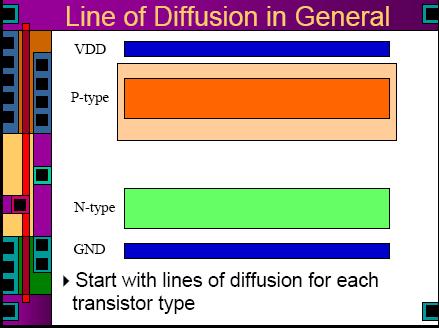
 UNIT III VLSI CIRCUIT DESIGN PROCESSES In this chapter we will be studying how to get the schematic into stick diagrams or layouts. MOS circuits are formed on four basic layers: N-diffusion P-diffusion
UNIT 3 Transistors JFET
 UNIT 3 Transistors JFET Mosfet Definition of BJT A bipolar junction transistor is a three terminal semiconductor device consisting of two p-n junctions which is able to amplify or magnify a signal. It
MOS Field-Effect Transistors (MOSFETs)
") 6 MOS Field-Effect Transistors (MOSFETs) A three-terminal device that uses the voltages of the two terminals to control the current flowing in the third terminal. The basis for amplifier design. The basis
6 MOS Field-Effect Transistors (MOSFETs) A three-terminal device that uses the voltages of the two terminals to control the current flowing in the third terminal. The basis for amplifier design. The basis
444 Index. F Fermi potential, 146 FGMOS transistor, 20 23, 57, 83, 84, 98, 205, 208, 213, 215, 216, 241, 242, 251, 280, 311, 318, 332, 354, 407
 Index A Accuracy active resistor structures, 46, 323, 328, 329, 341, 344, 360 computational circuits, 171 differential amplifiers, 30, 31 exponential circuits, 285, 291, 292 multifunctional structures,
Lecture 15. Field Effect Transistor (FET) Wednesday 29/11/2017 MOSFET 1-1
 Wednesday 29/11/2017 MOSFET 1-1") Lecture 15 Field Effect Transistor (FET) Wednesday 29/11/2017 MOSFET 1-1 Outline MOSFET transistors Introduction to MOSFET MOSFET Types epletion-type MOSFET Characteristics Comparison between JFET and
Lecture 15 Field Effect Transistor (FET) Wednesday 29/11/2017 MOSFET 1-1 Outline MOSFET transistors Introduction to MOSFET MOSFET Types epletion-type MOSFET Characteristics Comparison between JFET and
CHAPTER 8 FIELD EFFECT TRANSISTOR (FETs)
") CHAPTER 8 FIELD EFFECT TRANSISTOR (FETs) INTRODUCTION - FETs are voltage controlled devices as opposed to BJT which are current controlled. - There are two types of FETs. o Junction FET (JFET) o Metal
CHAPTER 8 FIELD EFFECT TRANSISTOR (FETs) INTRODUCTION - FETs are voltage controlled devices as opposed to BJT which are current controlled. - There are two types of FETs. o Junction FET (JFET) o Metal
Spiral 1 / Unit 8. Transistor Implementations CMOS Logic Gates
 18.1 Spiral 1 / Unit 8 Transistor Implementations CMOS Logic Gates 18.2 Spiral Content Mapping Spiral Theory Combinational Design Sequential Design System Level Design Implementation and Tools Project
Semiconductor Devices
 Semiconductor Devices - 2014 Lecture Course Part of SS Module PY4P03 Dr. P. Stamenov School of Physics and CRANN, Trinity College, Dublin 2, Ireland Hilary Term, TCD 3 th of Feb 14 MOSFET Unmodified Channel
ECE 340 Lecture 40 : MOSFET I
 ECE 340 Lecture 40 : MOSFET I Class Outline: MOS Capacitance-Voltage Analysis MOSFET - Output Characteristics MOSFET - Transfer Characteristics Things you should know when you leave Key Questions How do
8. Characteristics of Field Effect Transistor (MOSFET)
") 1 8. Characteristics of Field Effect Transistor (MOSFET) 8.1. Objectives The purpose of this experiment is to measure input and output characteristics of n-channel and p- channel field effect transistors
1 8. Characteristics of Field Effect Transistor (MOSFET) 8.1. Objectives The purpose of this experiment is to measure input and output characteristics of n-channel and p- channel field effect transistors
MOS Transistor Theory
 MOS Transistor Theory So far, we have viewed a MOS transistor as an ideal switch (digital operation) Reality: less than ideal EE 261 Krish Chakrabarty 1 MOS Transistor Theory Study conducting channel between
FET. FET (field-effect transistor) JFET. Prepared by Engr. JP Timola Reference: Electronic Devices by Floyd
 JFET. Prepared by Engr. JP Timola Reference: Electronic Devices by Floyd") FET Prepared by Engr. JP Timola Reference: Electronic Devices by Floyd FET (field-effect transistor) unipolar devices - unlike BJTs that use both electron and hole current, they operate only with one type
FET Prepared by Engr. JP Timola Reference: Electronic Devices by Floyd FET (field-effect transistor) unipolar devices - unlike BJTs that use both electron and hole current, they operate only with one type
EECS 151/251A Spring 2019 Digital Design and Integrated Circuits. Instructors: Wawrzynek. Lecture 8 EE141
 EECS 151/251A Spring 2019 Digital Design and Integrated Circuits Instructors: Wawrzynek Lecture 8 EE141 From the Bottom Up IC processing CMOS Circuits (next lecture) EE141 2 Overview of Physical Implementations
Organic Electronics. Information: Information: 0331a/ 0442/
 Organic Electronics (Course Number 300442 ) Spring 2006 Organic Field Effect Transistors Instructor: Dr. Dietmar Knipp Information: Information: http://www.faculty.iubremen.de/course/c30 http://www.faculty.iubremen.de/course/c30
Field-Effect Transistors
 R L 2 Field-Effect Transistors 2.1 BAIC PRINCIPLE OF JFET The eld-effect transistor (FET) is an electric- eld (voltage) operated transistor, developed as a semiconductor equivalent of the vacuum-tube device,
Lecture #29. Moore s Law
 Lecture #29 ANNOUNCEMENTS HW#15 will be for extra credit Quiz #6 (Thursday 5/8) will include MOSFET C-V No late Projects will be accepted after Thursday 5/8 The last Coffee Hour will be held this Thursday