The Ovation nx-amplifier
|
|
|
- Dinah Parks
- 6 years ago
- Views:
Transcription

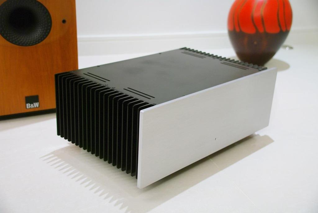
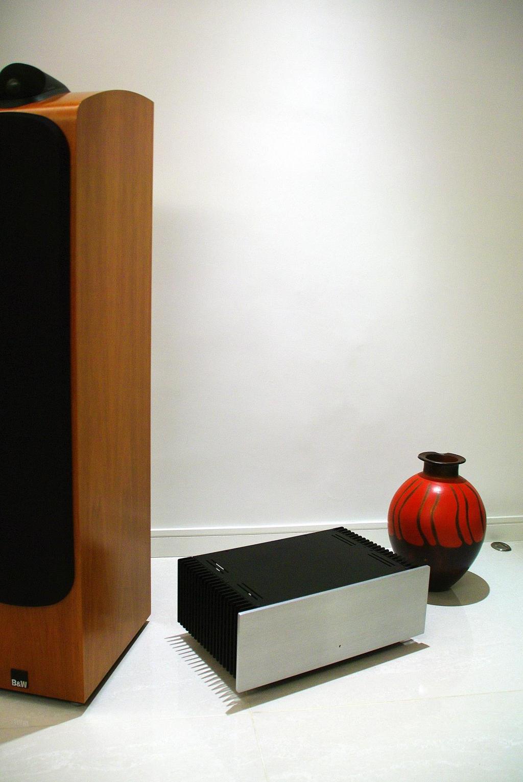
1 The Ovation nx-amplifier The Ovation nx-amplifier is a low distortion, very wide bandwidth (DC to 570 khz -3 db) 100 W CFA topology class AB power amplifier with amplifier distortion typically 70ppm at 100W into 8 Ohms, and about 50ppm at 1 khz. This design achieves outstanding DC performance with offsets of <10mV within 2~3 minutes of switch-on, and 1~2 mv after 10 minutes without the use of servos or DC blocking capacitors. The maximum offset at switch-on is under 50 mv. A PSU + Protection board provides DC offset, overcurrent and switch ON/OFF muting. This design leverages the front end of the class A sx-amplifier design published in July 2012, retaining the CFA topology and uncomplicated circuit design, but with a class AB output stage which enables it to deliver much higher output power. This is a compact amplifier measuring 42x27x150 cm s and weighing 12 kg. Amplifier board and PSU DSTHP PCB s (V2.0) are available for this design - see page 2 for details. Andrew C. Russell Updated November 2014 V Page 1
2 This document has been updated to reflect V2.0 PCB s for the nx-amplifier PCB and the PSU +Prot PCB Double sided THP gold Plated PCB s for this project are available from Jim s Audio nx-amplifier PCB Set The PCB set consists of two amplifier boards plus 1 PSU +Prot PCB Page 2
3 Page 3
4 Copyright The copyright for this document is owned by Andrew C. Russell All rights reserved This document may be freely distributed and copied, so long as it is done so in its entirely, and the authorship is acknowledged The Ovation nx-amplifier circuits, PCB layouts and all related documentation are made freely available for personal use and/or group DIY buys. If you are a manufacturer, kit supplier or DIY shop or any other commercial entity that wishes to profit from the design or derivatives thereof, you need to contact me at bonsai(at)hifisonix.com The diyaudio.com thread link to this project may be found here:- Check back here from time to time to see if there have been any further updates to this document:- This Project requires wiring up to the mains voltage. If you do not have the requisite skills or tools to deal with mains voltage wiring, get a professional to help you. Mains voltages are lethal exercise caution. Page 4

5 1. Introduction When the sx-amplifier was completed, I quickly came to the conclusion that if I re-configured the design for class AB operation and increased the supply rail voltage, I could easily scale the output up from 15 W RMS class A to perhaps 80 or 100 W class AB and still retain some of the essential design features of the sx-amp platform. I especially wanted to see if I could capture some of the magic sound staging and top end sweetness of that design in the nx-amp. The design goals remained simplicity, speed with rise times under 1 µs, very wide bandwidth along with good distortion performance. As I noted in the sx-amp write-up, the clipping behavior is important, and the nx-amp retains the soft clipping characteristic of the sx-amp design, something that is more usual in tube amplifiers. In this design, the amplifier PCB layouts are slightly modified to accommodate the additional driver stages, class AB bias control and short circuit protection, but the same compact PCB layout format is retained. The nx-amp features a more advanced power supply board incorporating speaker muting and basic protection features. However, if cost is a real issue, the sx-amp power supply board can be used as long as the filter capacitors are rated for 50 V and the capacitance is at least 22 mf per rail for a stereo amplifier. Note however, that if you do pursue this route, you will have to arrange your own DC offset protection and switch on and off thump muting you can read more about this in section 3 of this document. The mid-band loop gain on this design is moderate at circa 52 db, but not as low as the sx-amp. The distortion performance is thus somewhat better than the sx-amp at 70 ppm at 20 khz at 80 W output, and under 30 ppm at 1 khz. The nx-amp is a compact, cost effective design that sounds exceptionally smooth and open; just like the sx-amp, it is easy and fun to build with no compromises in audio quality. Figure 1-20 khz 1 V pk-pk Output into 8 Ω Page 5
6 1. nx-amplifier Specifications All specifications are into 8 Ω with +-45 VDC power supply rails unless otherwise stated Topology Rated Power Class AB Fully Balanced Symmetrical Current Feedback Amplifier (CFA) 100 W RMS class AB; 0.5 W in class A with bias set to 125 ma per output pair, 250 ma total bias 180 W RMS into 4 Ω Peak Current Capability ~5 A peak for 100 ms limited by fuses; 12 A minimum for 50 ms I 2 R capability ~500 W peak one channel driven Frequency Response DC 570 khz -3 db 1 W into 8 Ω DC 2.5 MHz front end filter disabled 1 W into 8 Ω Power bandwidth ~ 200 khz 1 Distortion (RMS) 80 W 8 Ω 0.007% at 20 khz; 15 W 8 Ω 0.003% at 1 khz 50 W 8 Ω.005% at 1 khz; 100 W at 0.15% distortion 20 Hz to 20 khz Distortion components at all rated powers below 100 W RMS predominantly 2 nd and 3 rd harmonics. Input Sensitivity & Impedance Noise Loop gain Closed Loop Gain Small signal rise time (10-90%) 1.2 V into 10 k Ω// [1 k Ω +220 pf]; ~10 k Ω at 1 khz -100 db ref 45 V pk output 52 db at 1 khz; 49 db; -3 db at 8.6 khz (simulation) 31 db; -3 db at 680 khz; phase lag <2 at 20 khz (front end filter in-situ) <550 ns with front end filter <100 ns with front end filter disabled Slew Rate >200 V/µs (front end filter disabled) c. 140 V/µs (front end filter enabled) (slew rate measured before the output LR network and into 8 Ω resistive load) Power Consumption Dimensions Weight 30 W at idle per channel 60 W for stereo amplifier (see text for discussion on OPS bias setting) 42 cm x 27 cm x 15 cm 12 kg 1 This is the full rail to rail output voltage swing into 8 Ω with no visually discernible distortion on the waveform Page 6
7 2. Circuit description and design discussion (See Fig 4) Front End Stages. The input signal is bandwidth limited by R17 and C13 before feeding buffers Q8 and Q10 (BC557C and BC547C 45 V Vceo) which in turn drive the bases of the level shifter stage, Q9 and Q11 ( BC546B and BC556B 65 V Vceo devices) which control the feedback node at the junction of R28 and R29 via their emitters. Collectively, these 4 transistors are referred to as the diamond input or front end stage. The input transistors derive their base bias via R10 (10 k). The front end emitter follower buffers are loaded via R34 and R35 which are fed from 10 V Zener regulators D3 and D4. This ensures that the quiescent operating current for the whole small signal part of the amplifier, including the TIS, is firmly fixed even with shifts in supply voltage of +- 20% 2. R36 and R37 (150 Ω each) provide some stand-off voltage to the bases of Q9 and Q11, so that their emitter currents can be stabilized by resistors R28 and R29 (120 Ω each).c6 and C12 provide heavy local decoupling of the Zener references. The collectors of Q9 and Q11 drive the TIS stage (Q6 KSC3503 and Q7 KSA1381) via the R30 and R31 collector load resistors. In a conventional CFA topology as would be found in an IC for instance, Q9 and Q11 would drive current mirrors, which would improve linearity and increase the open loop gain, but like the sx- Amp, I avoided that complication in this design as well in the interests of simplicity. Furthermore, in an audio power amplifier, the output stage presents a large, non-linear load to the TIS - the advantages one anticipates by going down this path are not easily realized, and especially so in the case of a EF2 design such as this one. The collectors of the TIS transistors Q6 and Q7 are tied together by the class AB bias control amplifier, configured around Q3, Q20, R6, R8,R20 and R21. This circuit simply multiplies (hence the commonly used name Vbe multiplier ) the base emitter voltage of Q3 which is dependent upon absolute temperature by the ratio of [R6+R20] and R21. We will come back to discuss thermal compensation a little later. Q3 acts as the shunt pass transistor, conducting most of the TIS standing current which measures about 28 ma in this design. C14 ensures that the Vbe multiplier circuit is stable and does not oscillate. Matching, DC Offset and Distortion. There is a lot of discussion around component matching and parts selection, and particularly so with respect to the front end diamond configuration (Q8 through Q11 in this design) and the two TIS transistors (Q6 and Q7). Matching for hfe and Vbe on the diamond front end will help to reduce DC offset and drift errors. Since in the nx-amp, the input Δ Vbe with temperature neatly cancel and in the prototypes and final build, after warmup and initial offset trim, amounted to 1~2 mv- a very good result indeed for a power amplifier. At low to medium frequencies, matching will also help to further reduce 2 nd harmonic distortion 2 Some designers have commented that using Zeners rather than current sources affects distortion. In sims, you may notice differences of about 1ppm in my view, this is too small to be of any practical concern at any level. Page 7

8 which will partially cancelled in symmetrical design amplifiers like this one in any event. At HF, layout and device differences will in many cases reduce this effect, but in my view, the benefits of matching are well worth the effort. See Section 4 for matching requirements and further information. CFA Front End operation class A or class B? Unlike VFA s, the peak current output from a CFA amplifier front end is not limited to a fixed maximum value (the tail current in a VFA), but is instead controlled by the feedback resistor value and the instantaneous output voltage. In practice, this means that high currents can be developed on demand to charge the compensation network, and this is one of the reasons CFA s achieve high slew rates and wide bandwidths as a matter of course. However, a number of commentators have remarked that the CFA diamond front end transitions from class A to class B and this could therefore impact the sound quality, the connection of course being with class B operation of the output stage where this definitely imparts a sonic signature, and a further concern that in a CFA this transition is taking place at small signal levels at the front end of an amplifier. Fig. 2 shows the currents in a diamond input stage model driven to full output. The source signal rise/fall times for this test were set to 10 ns impossibly fast for any audio signal to test the proposition that the input stage makes the transition to class B in a CFA front end. The amplifier Figure 2 - CFA Diamond output current no filter output is about 35 V peak (green trace) so it is definitely operating in the large signal domain and the front end filter is disabled. The yellow circles highlight that the level shifter current, i.e. the front end output current signal, just exits class A on the bottom edges of the waveform. But, as already noted, signals with these rise times in audio are not possible. Fig. 3 shows the same operating conditions, but with the input filter, designed to bandwidth limit the input signal, set to 1.5 MHz already much higher than the nx-amplifier which has an input filter cutoff frequency of 720 khz. To ensure that the front end always remains in class A in a CFA, the peak current provided by the feedback resistor should be less than the level shifter standing current under dynamic operating conditions. In a discrete power amplifier, this requirement is easy to meet. Page 8

9 Figure 3 - CFA front end showing no transisiton to class B front end filter in situ It s clear from Fig. 3 that the level shifter stage does not enter class B operation and stays firmly in class A see the yellow circles. What is interesting here is the current on demand behavior of the CFA front end the standing current in this model is c. 2.3 ma (red and blue traces), but goes to 4.2 ma peak (red trace) as required to charge the Alex Comp capacitor which was used in this model. In the previous slide, the peak current went to over 8 ma, just exiting class A operation but this only happened because the all important input bandwidth limiting filter was omitted. The conclusion from this discussion is that if sized correctly in terms of standing current wrt to peak feedback current, and the appropriate input signal filtering or bandwidth limiting is applied, discrete CFA input stages for audio power amplifiers can be easily designed to remain in class A at any input signal level. In IC CFA s, the general requirement to keep power consumption as low as possible means running the front end in class A is not a primary design goal, and the ability to transition to class B is instead exploited as an opportunity to reduce power consumption The Second Stage, or TIS. For the TIS devices, make sure you use devices of the same gain grade. Unfortunately the high gain grade devices are no longer available as pairs, so you have to use lower gain grades. This is quite ok and will not affect the performance as long as you use the same gain grades for both devices. The TIS runs at about ma standing current. With higher value TIS degeneration resistors, the spread of course is much smaller, but then there are other issues to contend with the 15 Ω used here is a good compromise. DC Coupling and Offset Adjustment. Like the sx-amp, the nx-amp is also DC coupled and R3 is a 10 k 22 turn potentiometer, connected across the front end +-10 V Zener regulators, and used to dial out the output offset during initial calibration; C1 simply filters out any Zener 3 or remaining rail noise so that it is not injected into the feedback summing node at the junction of R28 and R29. We will discuss the feedback and compensation a little later. Being DC coupled throughout can be problematic if the preamplifier output has a DC offset. A 20 mv offset at the preamp output becomes a 750mV offset at the output of the nx-amp which 3 On a typical 10 V or higher Zener, the wideband noise is 3~5uV, whilst the output impedance is in the region of 2~ 5 Ω and dependent on the Zener current Page 9
10 is most assuredly a big issue the DC offset detection will be activating continuously and a 750mV DC bias on the speakers is going to seriously affect the sound. The input driving source offset must be no more than 1 mv which should not be a problem for modern opamp based preamplifiers. The other option here is to capacitively couple the preamplifier to the nx-amp input using a 100 µf 50 V electrolytic capacitor in parallel with a good quality 1 µf 50 V or 100 V film capacitor (See appendix 7). Also, note that when you adjust the output offset (see section 5), this must be done with the inputs to the nx-amp disconnected - you do not want to be dialing out the pre-amp offset if there is one connected to the input and it is DC coupled as it can cause other problems. Page 10
11 Note: do NOT fit link across J2 on PCB +150mV -150mV +10V -10V ~1.1V ~1.1V 82mV Q9 BC546B * +140mV -140mV BC556B Q11 * ** * * * * * * * = SMD **=SMD mounted on underside Figure 4 nx-amplifier V W Class AB CFA Amplifier Circuit Diagram Page 11

12 Output Stages. The TIS stage drives an emitter follower double (EF2) output stage, with Q12 and Q13 forming the driver stage, and Q1, Q2, Q4 and Q5 the output stage devices. Q3 and Q20 form the bias spreader, with R5 setting up the driver stage quiescent current at 35 ~ 40mA whilst C10 speeds up the turn off performance of the output devices when conduction transitions from one half to the other. For the output devices proper, I chose NJW3281 and NJW1302 sustained beta devices, using 2 pairs to improve thermal management, and to reduce distortion by minimizing beta droop. You can use slower devices like the MJE21193/ you however may have to adjust the value of C7 to stabilize the loop. Distortion with these transistors will be about 1.5 to 2x higher, but I cannot say what effect, if any, it will have on the nx-amps actual sound. In the prototype and final builds, I used the same transistor types for both the TIS and driver stages, which some people have commented on as being wasteful, since high performance TIS devices are becoming rarer, and especially so in through hole form. Fairchild KSA1220A/KSC2690A devices (or the original Japanese types 2SA1120A and 2SC2690A) make fine drivers for this design, whilst preserving the precious stock of 1381/3503 low Cob TIS transistors. Its important that the same gain grade is used for the drivers as well, and I recommend O or Y suffix versions. The EF double (or EF2) output stage allows the nx-amp to realize 80 W RMS output with distortion of about 70 ppm, and at the onset of clipping at 100 W 0.15% (figures at 20 khz and +- 45V supply rails). A triple would have reduced the 80 W figure to well under 10 ppm (with some adjustments to the TIS standing current), but in my view, the additional benefit would have compromised the aim of a simple, high performance design. As I remarked in the sx-amplifier write-up, in general there is little correlation between perceived sound quality and total system distortion 4 below about 1%, and as you should conclude, I am not wedded to single digit or sub ppm distortion levels as an overarching amplifier design philosophy the only value in single or sub ppm digit distortion levels is in the technical challenge both in terms of circuit design and execution. Figure 5 - nx-amp at 100kHz 6V pk-pk For this design, I set the output stage standing current a little higher than class AB optimum bias theory (the so called Oliver voltage ) suggests, which is about 78 ma per output device (from Ib = 0.026/(Re+ re) where (Re + re) is the total output transistor emitter degeneration resistance, including the internal emitter resistance), instead going 4 See interesting write up here Page 12
13 for around 125 ma each 5. The total standing current of each channel is therefore 300 ma, including front end circuitry. The heatsinks are rather substantial, so the temperature rise over ambient is only 10 C when idling. During listening tests, I got the impression the amplifier sounded more euphonic with the higher bias setting, and so that is what the nx-amplifier is set at. Note that the distortion figures quoted in the specs are simulated at 78 ma per output device the higher bias setting figure I used will result on about 15~20 ppm more distortion across the board. The nx-amplifier bias current is very stable, with Q3 (BC847C) providing the thermal compensation. I few people have asked me how come Q3 is not attached to the heatsink. The BC845C SOT23 device has a very low thermal mass, and since it is placed on the underside of the PCB and close to the collector lead of the output device, tracks temperature rather well. Further, the drivers are also attached to the heatsink and while not quite isothermal, nevertheless track closely enough to provide good performance. I did experiment using a small amount of thermal grease to couple Q3 to the output device collector lead, but found this provided little or no improvement. Note that an EF2 is much easier to thermally compensate than a triple, where there is a 6 Vbe voltage stack to deal with. You can read about how I did this on my output triple e-amp design. 6 R41, R42 along with the 4.7 Ω W SMD resistors in the bases of the output transistors are stoppers that prevent parasitic oscillation which can be a problem when using fast output devices in the EF2 configuration (and this problem almost a certainty with an EF3 output stage if precautions are not taken). In the final design, R41 and R42 in the driver transistor bases were fitted with 0 Ω 1206 jumpers, but you can also just link them neatly with a blob of solder. R5 which is fitted between the emitters of the driver transistors Q12 and Q13, sets the driver stage standing current at about 40 ma while C10 (0.1 µf film) assists in speeding the turn off time of the output stage devices. For the most part, the driver stage operates in class A, only transitioning to class B at high power levels. Its interesting to contrast this with the e-amp, which uses a triple follower, and in that design both the pre-driver (as would be expected) and driver stages run in class A all the time, with the drivers only transitioning to class (A)B at 800 W output i.e. a very heavy sub 2 Ω load. 5 Most of my designs have the output stage Iq set simply by 0.026/Re, so they are generally about 15~20% higher than they should be. 6 See page 37 in the e-amp write-up Page 13
.")
 play a key role in enabling this type of HF performance which would not be possible with legacy parts.")
14 The two scope shots on this page give some idea of the wide bandwidth and rise time performance of the nx-amplifier. In the uppermost shot, the amplifier is delivering >50V pk-pk at 20 khz into an 8 Ω load (scope probe is 10x). The waveform is clean with no overshoot and the waveform tops show no ringing (a sure sign of board decoupling problems on a test like this). Certainly, modern 30 MHz Ft output stage devices (NJW3281, NJW1302 and derivatives) play a key role in enabling this type of HF performance which would not be possible with legacy parts. The second scope shot below shows the amplifier output waveform at 100 khz into 8 Ω at about 70V pk to pk (scope probe is 10x). This is an extremely stressful test that exercises the output stage devices, drive and recovery performance. If the output devices are not being switched cleanly, and the base charge on the device being switched off removed quickly, cross conduction and cross over anomalies would be evident. In the nx-amp, the driver stage tie resistor (R5 33 Ω) is purposely kept low, assisted by C10 (0.1 uf), which facilitates the good switching performance you see here. Both of these scope shots were done with the front end filter in situ and the Zobel disconnected and R36 and R37 at 150 Ω and R28 and R29 at 120Ω per the V2.0. The 10-90% rise/fall time of these waveforms was measured at ~700 ns. Page 14


15 Figure 6 - +ve Rail Noise Before Filter Figure 7 - Zoom-in on HF Noise Power Supply Rejection Ratio and Decoupling. One of the drawbacks with CFA topology amplifiers is their lower PSRR something well designed VFA topology amplifiers really excel at. To mitigate this shortcoming, the front end stage is heavily filtered (R22, R23 along with C5, C8 and C9 and C11) and Zener regulated (D3 and D4). A ripple eater or AFEC would also help significantly here, but that will have to be something for another project this one is about keeping it simple. Figs. 6~8 show the waveforms on the +ve supply rail before and after the filter while the amplifier is delivering 60 W into 8 Ω at 20 khz. One of the questions I was asked was why not use a larger filter for even better ripple rejection? The answer is primarily linked to the value of the series resistors which are 15 - making them higher reduces the available output swing. With the values shown the drop across the 15 resistors (R22 and R23) is around 0.45 V. You can of course increase the value of the filter capacitors, but I think the 220 µf I specified is a good compromise between performance, size and cost, which figures 6 through 8 seem to bear out. The rails are decoupled directly after the fuses with 220 µf 50V capacitors (C2 and C4) and the tracks between these capacitors and the output devices are extremely short. This is a high speed design, so it is important that the supply impedance remains low out to at least about 1 MHz. During prototype testing, I used 0.1 µf film capacitors only, and ended up running about 500 mm of cable across the positive fuse holder to an ammeter. The positive tops of the square wave output test signal Figure 8 - +ve Rail Noise After Filter showed ringing and I initially presumed it was to do with compensation and the load. However after some investigation, it became apparent that the decoupling was inadequate, and In a practical amplifier, I had to consider the cabling from the PSU to the amplifier board as well, so the problem was resolved by fitting C2 and C4 (220 µf 63 V). Incidentally, the sx-amp design and PCB was also upgraded in this way as a result of the findings on the nx-amp. The inductance in the supply rails between the decoupling capacitor is only about 20nH, ensuring the volt drops at HF are low. A 1 A step change in 1µs, again impossible in a real world bandwidth limited audio signal, results in a drop of about 20 mv with the capacitors as shown. On designs where there is significant inductance in the rail tracks between the power source and the output devices, local decoupling is required in the form of a substantial value electrolytic and a 0.1 µf film in parallel. Page 15
16 It should then also be remembered that the decoupling component return paths to 0 V are just as important. Each supply rail on the nx-amp is fused with 5 x 20 mm 5 A fuses, which are sized to cater for situations where the load impedance will drop to 4 or 3 Ω, and the amp will be running in class B and drawing over 5 A more or less continuously. Short term peaks of 12~14 A can be sustained for some 100s' of ms without popping the fuses, or triggering the short circuit protection 7. D1 and D2 provide reverse polarity protection in the event a fuse opens, thereby preventing the semiconductor junctions from being reverse biased, which could lead to damage. Speaker Coupling and Real World Capacitive Loads. The speaker is coupled to the output stage by means of L1 (see Appendix 1 for winding details), a 0.6 µh inductor in parallel with R9, a 3.3 Ω resistor. At high frequencies, this network isolates the amplifier from any capacitive loads, ensuring that it remains stable. Further, directly off the output, before inductor, I have fitted a connector for a Zobel network which is located on the PSU PCB. At high frequencies, the Zobel network ensures the amplifier sees a load that approximates 8 Ω, also aiding in overall stability. Note that you cannot drive the amplifier at HF at high frequencies (e.g. 100 khz) without smoking the Zobel resistors typically something you might try during bench testing - so make sure you disconnect the Zobel network when doing high power HF testing. However, under normal operating conditions, there is not much energy above a few khz, so this problem will never occur in practice (the Zobel load resistor is rated at 6 W). A lot of effort was expended in making sure that the nx-amp would be extremely robust, and able to drive any real world load. As you will see a bit later, because of the loop gain and wide bandwidth objectives, I ended up with a ULGF of over 3 MHz (simulation), which is at the upper limit for an EF2 bipolar output stage design for an EF3 like my e-amp design something around 1~1.5 MHz is about as high as you can go whilst still preserving adequate gain and phase margin. It would not be possible to be able to claim unconditionally stable with any load without adding the output coupling networks just described. These ensure that the nx-amp has plenty of gain and phase margin, despite the high ULGF, with any load. Extensive bench testing of the nx-amplifier with capacitive loads from about 500pF up to 2.2uF and load resistances from 2 to 15 Ω confirmed that it is unconditionally stable. 7 Note that short circuit protection is not provided on the basic PSU board. Page 16

17 Figure 9 - nx-amplifier Clipping is Soft As can be seen from Fig. 9, the nx-amp, like the sx-amp, clips quite softly relative to some solid state designs, with a very smooth recovery as it exits overdrive. One of the things I have noticed about low open loop gain CFA topology amplifiers is that generally they exit clipping very cleanly, whereas often in VFA designs, you have to take special precautions to deal with rail sticking. There are a number of reasons, but part of this can be attributed to the fact that the feedback loop in CFA s is generally faster, and the error drive thus lower. Of course, the lower loop gains associated with CFA designs also help. Protection. For short circuit protection, the volt drop across a pair of emitter degeneration resistors (0.33 Ω 5W each) is sensed by R2, R7 and fed into the LED emitter of a random phase triac opto (U1 FODM3012). At about 12~14 A peak, the opto-triac will trigger and latch, and the output, at J1 (SC) will clamp to the minus supply rail, disengaging the solid state loudspeaker relay on the power supply and protection board. The response time to a dead short on the output to speaker disengaged state is about 50 µs so considerably faster than the fuses (F1 and F2). This protection mechanism is non-intrusive, unlike methods that sense the output current and then clamp the drive to the output stage, which is the conventional way of doing things. After a short circuit trip, the amplifier power will have to be cycled OFF until the power LED s are completely extinguished, then ON again. Given the 180 Watts on tap into 4 Ω, this will be a very rare occurrence for the most part. Fuses F1 and F2 are rated at 5A and provide the last line of defense in case of gross failure of the output stage. Page 17

18 Feedback and Compensation Components. The feedback resistor network (R12~R16) is made up of 5 metal film resistors connected in parallel. Since this is a CFA topology amplifier, the feedback resistor values are low and as a result the associated current through the resistors is substantial. The combined value is 540 Ω which dissipates about 2 W when the nx-amp is delivering 40 V peak. The devices specified have low tempco s, which minimizes thermal distortion, always a consideration for the feedback resistor in power amplifier. Its also important that these devices have low voltage co-efficient luckily this is a feature of good quality metal film resistors, so almost any reputable brand name will be suitable. C7 and C13 should be decent quality silver mica, NPO ceramic 8 or polypropylene capacitors. For the TIS transistors, stick with the KSA1381 and KSC3503, which are low Cob types especially suited to this function. The nx-amplifier is capable of delivering a first class listening experience, so my recommendation is you don't skimp on these components. 8 NPO ceramic capacitors are very good for this type of application and suffer from none f the proble3ms associated with other ceramic dielectrics like XR5, Y5G to name two Page 18
19 Page 19
20 3. Compensation Matters If you have read my other amplifier design write-ups at you will recall that I generally like to design with plenty of gain and phase margin in hand, both for solid technical reasons, and in my experience because amplifiers that are stable and can handle any real world load sound better. Back in the early days of solid state, and before there was a clear understanding of how to really design a linear amplifier and how to compensate them properly, designers often applied excessive amounts of feedback in order to achieve low distortion figures. In doing so, gain and phase margins were for the most part insufficient, and there were all sorts of stories about certain amplifiers requiring specific types of cable to sound right, or to remain reliable i.e. not go up in smoke due to HF oscillation that fried the output devices due to cross conduction especially a problem in the old, slow output transistors like the 2N3055/2N2955. Tube designs never seemed to have instability issues because the loop gains are lower i.e. designers can get away with simple compensation schemes which historically was especially convenient since the analytical tools like Spice that we have today were not available then. Compensation has a critical bearing on the performance and sound of an amplifier. Get it wrong, and the finished design will be sub-optimal in every respect; getting it right is key to high performance. For the nx-amp, I used LTSpice to explore the loop gain and phase in conjunction with practical real world testing on the bench. The nx-amplifier is a CFA topology design and uses Mark Alexander s CFA compensation approach. In the appendix of his application note, he discusses the technique of returning the compensation capacitor (C7 68 pf in the nx-amp) back to the feedback summing node (junction of R28 and R29), allowing the comp cap value in his specific design to be halved, whilst still preserving the overall loop stability, but with an improvement in loop gain phase and gain margins especially useful at HF. This looks a bit like MIC in VFA topology designs, but the operation detail is somewhat different if you look at the math. In the nx-amp, if C7 is returned to ground in the conventional manner, it would need to be increased to 1nF to achieve the same ULGF. Alternatively, the feedback resistor values can be increased (this is the recommended approach for IC CFA s), but still maintaining the same ratio, such that if we keep C7 at the original 68pF but connect it from the TIS output to GND in shunt mode, the feedback resistors need to go to 4000 Ω and 111 Ω respectively. Both of these options bring the needed stability, but at the expense of slew rate and HF loop gain. Some CFA amplifier designs use Cdom around the TIS stage. This works, but you need two caps in balanced design such as this one, and you can sacrifice slew rate if not careful. Page 20
 but still with nearly 80 degrees of phase margin in hand, while there is about 15 db of gain margin.")
21 Plot 1 - nx-amplifier Loop Gain and Phase into 8 resistive load Plot 1 shows the ULGF locates at ~3.5 MHz (high and at the upper limit for EF2 designs) but still with nearly 80 degrees of phase margin in hand, while there is about 15 db of gain margin. L1 isolates any load capacitance (cabling, speaker crossover) from the amplifier output stage. Now, it is possible to eliminate L1, but this would require that the ULGF be lowered, and the consequence of that would be less loop gain from 5 or 6 khz to correct distortion, and less feedback to correct distortion at LF, where the response is flat. I have experimented in the simulator with two pole Alexander compensation on CFA topology amps, and they appear to be stable, and you can eke out another db of loop gain at HF something to explore in more depth in a future design perhaps. Extensive practical testing with a wide range of capacitive loads confirmed that the nx-amplifier is unconditionally stable with any output load from > 3 (the lowest value tested) in parallel with any capacitance from 50 pf through to 2 µf. Page 21

22 Plot 2 - Gain and Phase Margin without L1 and 10nF Load Capacitance; without a reduction in loop gain, instability is assured with higher capacitive loads Plot 2 shows what happens when L1 is shorted out and 10nF of total capacitance connected to the output. Still stable, but there s not much room left before oscillation is likely to occur just a few nf and peaking up above 10 MHz that s sure to pop up above 0dB and cause stability problems. Certainly any lumped cable inductance is likely to reduce the chances of oscillation, but then you would need to be sure that you were not driving electrostatics or other heavy loads that would impact phase margin. All of my amplifier designs can tolerate a wide range of capacitive loading because of the healthy loop margins, and the use of an output coupling network comprising L1 and associated damper resistor in this case R9. Plot 3 shows an absolute worst case condition where the amplifier drives a 2 µf // 2 Ω load something you might find on an electrostatic speaker for example (although the load impedance might not dip quite this low). Without the coupling inductor, this amplifier would be oscillating, but 0.6 uh is sufficient to allow it to drive any conceivable load without compromising stability. The upshot of all this is that the designer can, if they so wish, apply more feedback at mid to HF to reduce distortion, by setting the ULGF higher as already noted, in the nx-amp the use of the output coupling inductor allows this to be set at 3 MHz. The notch at ~138 khz is the resonant frequency of the load capacitance and the output coupling inductor. R9, and the speaker resistance, act to damp this somewhat, but when driving a real world load with a square wave source, you still get ringing as depicted in Plot 4. Page 22


23 Note that even in amplifiers that do not employ an output coupling network, ringing is also evident when measured at the speaker terminals, but usually at a higher frequency. Some designers employ termination networks like the Zobel shown in Fig 13 (C7 and C8 and associated components) at the amplifier output and at the speaker terminals to reduce ringing, although the effectiveness of this technique has been questioned by some experts. Plot 3 - Worst case 2 µf//2 Ω Load with L1 in Situ Plot 4 - nx-amp output across 8 // 1 µf load with 25 khz square wave input Page 23
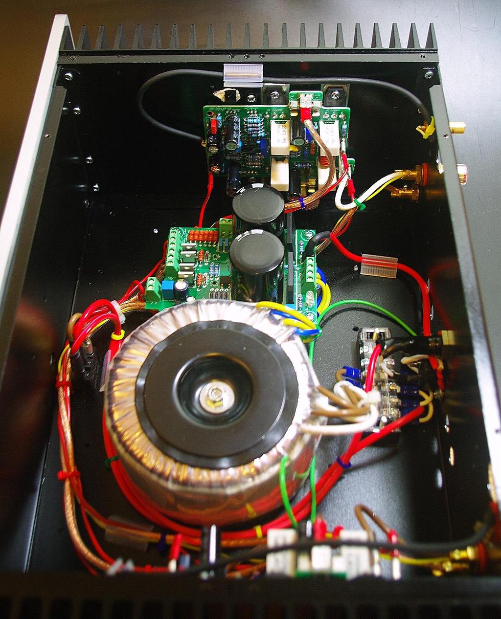
24 Power Supply and Speaker Mute Board Solid State Loudspeaker Relay (SSLR) Refer to Fig. 13. We will start off by looking at the operation of the solid state loudspeaker relay (SSLR) consisting of Q4 and Q5 Q1 and Q2 for the other channel operate in exactly the same manner. When U1 is in the OFF condition, R8 (22 k) pulls the gates of Q4 and Q5 towards V- effectively removing their gate drive, and they are therefore OFF. During the turn off event, D7 (12 V Zener) is forward biased, clamping the gate to the source of the mosfets to -0.7 V, preventing any high voltage reverse gate bias damage. R9 (3.9 k) provides a bleed-off path for any residual gate charge. The turn-off speed is highly dependent upon the drive waveform to the gates and the source impedance, but in this design it is in the region of about 50 µs. To turn the SSLR ON (or to engage it) R10 (5.6 k) is pulled to V+ by the action of U1, which is controlled by the protection and delay circuits. This forward biases the gates of Q4 and Q5, turning them ON and connecting the Spkr Return point to the power supply 0 V via the drain of Q5 which is connected to 0 V. D7 clamps the gate-source voltage to 12 V, ensuring the mosfets are not damaged. The turn ON time is about 25 µs. D13 provides simple diode steering, ensuring that short circuit protection (SC via J7) from U2 random phase triac opto on the amplifier board has priority when it clamps to V-. The SSLR in this design is implemented using 100 V TO220 Trench NextFET technology devices from NXP (part number PSMN4R3-100PS) that feature an Rds (on) of 4.3 mω, for a total SSLR end to end resistance of under 10 mω. This is significantly lower than any readily available electromechanical relay, and the NextFet solution can take some serious abuse for example like cleanly switching fault currents as high as 50 A in <50 µs. Further, since there is no contact wear out mechanism, long term reliability is further assured. Provided the operating envelope remains within the absolute maximum thermal and electrical specifications of the mosfets, these devices can switch speaker fault loads day in and day out, year after year and that includes inductive dump, for which these devices are rated at over 500 mj. No electromechanical relay of similar size and cost can do this. Power Supply The split secondary windings from the transformer (See Appendix 2 for transformer specification) are fed in via J3 and J2 J2 is the common point and is connected to 0 V. A 20 A PCB mount bridge rectifier (D12) feeds two 22 mf ( micro Farads) 50V capacitors (C 6 and C 9), providing rectified and smoothed DC out on dual Phoenix screw connectors J5 (V+) and J4 (V-), with the 0 V Ground connections at J1. Like the sx-amplifier, the nx-amp Zobel networks Page 24

25 are mounted on the PSU board (3 x 33 Ω 2 W wire wound resistors in parallel along with associated 100 V film capacitors C7 and C8). R21, R22 and D10 and D11 provide power indication and bleed off of the capacitor charge when no load is connected. D9, also a 20 A bridge rectifier, provides a ground lifter function, and this can be useful in breaking ground loops in systems that suffer from hum. See Rod Elliot s detailed description here for more information about grounding. Figure 10 - An Early Prototype of the PSU +Protection Board DC Protection and Speaker Muting The second set of functions provided by the board is DC detection, speaker muting and output short circuit shutdown. For DC detection, the output from the amplifier is wired into the protection board via J10 (mini 2.54 mm pitch 3 way Phoenix screw terminal block). R13 and R14 (22 k) provide pull downs to ground, while R15 and R16 (100k) along with C4 and C5 form a low pass filter (-3 db Fo ~0.15 Hz), with D8 bridge rectifier arranged to provide a clamp of V. The output of the filter feeds into Q6 and Q7 active rectifiers. If the DC potential across C4 + C5 goes +ve by about 1 V wrt 0 V, Q7 will turn on, and likewise, if it goes ve 1 V across C4 + C5 wrt Page 25

26 0 V, Q6 will turn on. In the event of the output of the amplifier going to one of the rails due to a catastrophic failure, this filter and the protection circuit would disengage the speakers in about 10 ms. With a 1 V DC offset, the protection triggers in about 800 ms. Due to the circuit configuration, the gains from the two transistors are not symmetrical, with the positive detection via Q7 being much more sensitive, since it is operating in common emitter mode with high gain, while Q6 operates in common base mode where the current gain is ~1. This is remedied somewhat by ensuring the collector load of Q6 and Q7 is high and tied to a high supply voltage (V+ in this case, which is at the main supply rail voltage up at over 45 VDC) via U3, which is a 100 k PNP RET (NXP part type PDTA115ET). If DC on the amplifier output is detected, U3 s output switches HIGH, pulling NPN RET U2 (NXP PDTC144ET) output LOW and shunting the gate of Q3 (2N7002) N-channel mosfet LOW via R1. This in turn switches 10k PNP RET U1 (NXP PDTA144ET) OFF, removing drive from the SSLR. These SSLR s are connected to the speaker ground return line via J9, a Phoenix twin screw connector. This mosfet gate drive approach makes for a simple, neat way to switch the speakers without recourse to opto s which is the more normal way. Speaker switch ON/OFF muting is provided by the delay circuit built around Q3 (2N7002) and associated components connected to its gate. The secondary AC is fed via C3 into a half wave rectifier (D4 and D5); C2 (1 µf poly) provides some initial smoothing, and R7 (20 k) a light load, with D17 (4V7 Zener) providing clamping. This then feeds through R6 (100 k) into C1 (100 µf 50 V). The Figure 11 - Work on the Prototype nx-amplifier switch on delay with this configuration is about 4~5 seconds after which Q3 switches on, engaging the SSLR s. When AC power is removed, C1 discharges rapidly via D3 (BAS21H) and R7 in about 500 ms, disengaging the SSLRs. In both power up and power down cycles therefore, any speaker thumps are removed. J7 (marked SC ), a dual screw terminal Phoenix connector, provides a short circuit detect input. If this input is pulled to V-, it immediately disengages the SSLR. On the nx-amplifier, the opto triac is used to detect the output current, and if greater than about amps, it will latch on, clamping SC to V- and turning the speakers OFF. Page 26

27 However, note that with the SSLR approach shown here wherein the return line of the speakers is switched, if the speaker hot line is shorted to the chassis, the SSLR is effectively bypassed, and no protection other than the amplifier board fusing is provided. Figure VA Power Transformer Page 27
28 Power Supply Protection Figure 13 - PSU +Protection V2.0 Board Circuit Diagram Over current Trip input Solid State loudspeaker Relay Page 28

29 With this over current protection scheme, you can short the speaker output of the nx-amplifier when driving full power, and the SSLR disengages the speaker within a few 10 s of microseconds; on a relay based protection set-up that does not incorporate current limiting the relay will likely be damaged, or worse, the amplifier output stage devices are likely to self destruct before the fuses open. As mentioned above, the peak amplifier output current under these conditions is in the region of 12~14 amps, but because the protection circuitry and SSLR react so quickly, the 5 A rail fuses remain intact - this protection scheme is thus completely non-invasive up to the trip point. This approach avoids any impact on the amplifier sound which can happen with schemes that use current sensing across the output device emitter degeneration resistors and then clamp the driver transistor bases. R27 (2.7 k) and D15 LED provide speaker enable indication; note however, if the SSLR disengages due over current, this LED still remains illuminated, but D16, a small SMD LED mounted on the PCB, will also illuminate. I have included these LED s because they make debugging and fault assessment much easier besides, LED s look good. It is important to note here that the triac opto used here (FODM3012) is a random phase triggered type. Zero crossing types will not work in this circuit because for example, if the amplifier output is shorted to one of the rails, say in the case of an output stage device failing, it will not get the opportunity to pass through 0 and therefore allow the triac to latch. Figure 14 - nx-amplifier board and PSU +Protection Page 29
30 Some constructors of the earlier V1.0 nx-amp PSU +Protect board encountered a few problems with the mute circuit not engaging after applying power. In recognition of these issues, I changed C3 from the original 0.47 µf to 1 µf and R6 from 330 k to 100 k on the V2.0 board. Although my 3 V1.0 prototype boards worked perfectly with the original values, its clear the value selections were somewhat borderline. Note that for the delay circuit to work correctly with the values shown, the secondary AC voltage needs to be between 30 and 34 VAC. Anything much below this, and the value of C3 will have to be increased best solution is to wire a 2 nd 1uF cap in parallel with C3 underneath the PCB. One builder, Bill_P, from the USA solved the problem of the SSLR not engaging by increasing the value of R7 from 5.6k to 22k. I have incorporated his suggestions into the V2.0 boards, as well as changing U1 to a PDTA144ET (47k internal resistors) to limit the dissipation, which was an issue with the original device I selected. Here are a few notes to help you with debugging:- 1. For initial testing, hook up the PSU +Protect board but do not connect the amplifier boards yet. 2. Apply power and check that the SSLR engages after about 5-8 seconds (D15 should illuminate) 3. If it does not, then make sure that the voltage on the collectors of Q6 and Q7 is at V+ (this will be the main rail voltage up at about +50 V). If not, power down and then lift R1 (100 SMD resistor) after which you can power up again. If the SSLR then engages, there is a problem in the DC detect circuit. Check to make sure that Q6, Q7 and the circuit in front of it is operating correctly. Of course, also make sure that there is 0 V DC voltage at J10 pin 1 and pin If lifting R1 does not solve your problem, you need to look at the delay circuit. 5. The 2N7002 (Q3) is specified to turn on at 2.5 V max (250 µa drain current) and some devices will already turn on at 1V. Ideally you should measure 3 V and higher at the gate of Q3. Of course D17, a 4.7V Zener, will clamp the voltage so you should not be measuring more than 4.7 V +-5%. 6. Note that it is important that you have the RET s (resistor equipped transistors) installed in the correct locations U1 is a PDTA144ET which provides a 47k load to Q3 make sure you have not accidentally installed Q3 (100 k PDTA115ET) in this location because you are likely to get problems (the SSLR mosfets will not switch on hard enough - this will cause distortion and they will also run hot) 7. If the gate voltage is correct per 5 above, but you still don t see the SSLR engaging, measure the voltage at the drain of the 2N7002 Q3. If it is not at 0 V, the mosfet or delay circuit has a problem. If the drain is measuring close to the v+ rail (so, up near 50 V), its clearly not switching on. 8. To make sure that the problem is not after the gate of Q3, you can short drain of Q3 to 0 V (just switch your meter to current and then put the probes across 0V and the drain of Q3). If the SSLR then engages, you know that everything after the gate of Q3 is ok your problem is on the gate side of Q3 again, if you are measuring 3 V or higher at the gate of Q3, your mosfet is probably damaged. 9. Once your PSU +Protection board is working (NB don t forget to reconnect R1 if you lifted it!) you need to do the following tests:- a. Power up the board and let the SSLR engage. Switch your DVM to and measure across each of the SSLR s. You should measure 0. To double check that the gate drive is correct, measure across D1 and D7 you should measure ~12 in each case b. Next, take a 1.5 V AA or AAA cell (make sure they are new and measure the correct terminal voltage). Connect the cell across J10 pin 2 ( this is 0 V) and pins 1 and then 3. In both cases the SSLR should disengage. Note, it may take up to 1 second this is perfectly ok with a 1.5V Page 30
31 offset. Now turn the cell around and redo the test - the SSLR should disengage after about 1 second. This s the low voltage offset test. c. Finally, use a 1k resistor and connect J10 pin 1 directly to V+ - the SSLR should disengage almost instantly; then connect it to V- and you should get the same result. Repeat the test on pin J10 pin 3 you should get the same rapid disengage result on both V+ and V- (Be careful not to short pin 2 of J10 to V+ or V- that s why you should use the 1 K resistor). This completes the testing of the PSU +Protection board. Page 31
, required for good thermal compensation.")
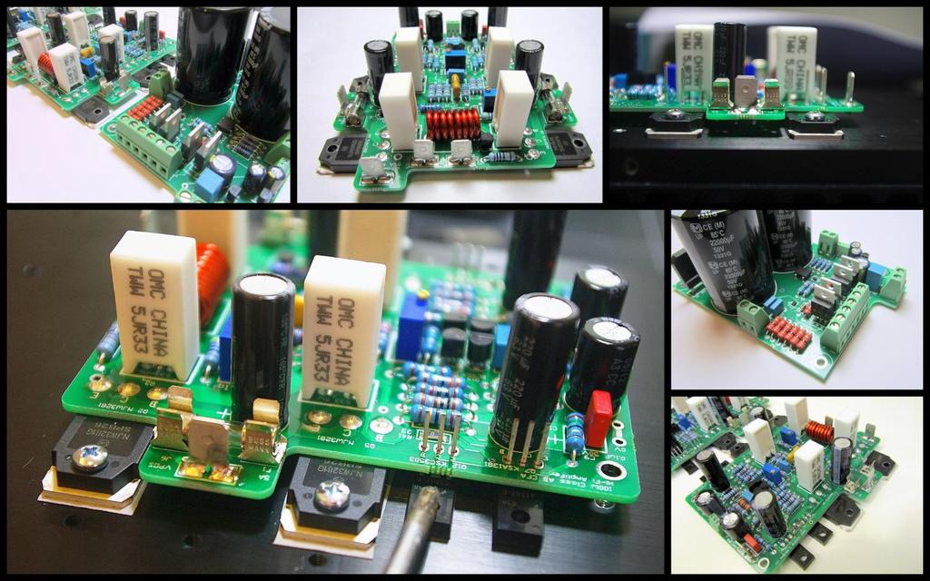
32 4. Construction, Parts Selection and Matching Both the amplifier boards and the PSU + Protection board utilize some SMD components. I did this because they are convenient, save a lot of space and in the case of the bias spreader (Q3 BC847C on the amplifier boards), required for good thermal compensation. To solder SMD devices, you will need a good quality, fine tipped soldering iron, and a pair of fine tipped tweezers and some 1 mm or less diameter solder. Take a look at Dave s EEVblog Youtube video here for some inspiration and guidance. Once you get the technique, soldering SMDs' is great fun and placing SOT23 or tiny SC457 parts neatly can be quite cathartic. Figure 15 - Top and underside view of the nx-amp PCB assembly prior to mounting the TO-126 devices Each channel of the complete nx-amplifier, as shown in Figure 4 and in the Fig 15 photograph above, is constructed on a small PCB. I like to sandwich the output devices between the PCB and the heat sink, but in this design, to keep the board as small as practicable, the devices simply connect to the edge of the board note however that the PCB actually rests on the edge of the packages of the output devices, so they effectively act as spacers. All connections to the board are via 5 mm push on tabs, except for the input connections where I used a small 2.54 mm pitch Phoenix screw terminal connector, which allows for easy removal if you ever need to service it. To start off, mark the holes on your heatsink using the finished boards as a guide. Drill and tap to M3. Take care with this procedure as breaking off a tap in a heatsink generally means you have to scrap the heatsink, or move the location of the PCB either way, it's a botched job, so take extreme care. For assembly, you should start with the SMD components first on all the boards (both sides), followed by the conventional resistors then capacitors and finally the small signal transistors, but NOT any of the power devices Page 32


33 including the TO-126 drivers and TIS transistors. Once this is done, and you have checked your work against the circuit diagram and component overlay, you can proceed to fitting the power transistors as described below. Figure 17 - TO3P Lead Bend To mount the TO3P power devices, start by bending the leads at 90 degree angle as shown in Fig 17. Now mount the power devices onto the heatsink in their correct locations wrt the PCB, screwing them in place, but not tightly at this stage. Next, carefully fit the PCB in place. This is quite tricky, because you have to align the holes on the PCB with the transistor leads which are facing up at 90 degrees. Once in then place, make sure the transistors are nice and straight and screw them firmly in place (i.e. so they don't move); next screw the PCB lightly in place via the mounting holes but make sure the PCB is not flexed in any way you simply want to keep it in place for the next operation. Your board should look like that in Fig. 16. Now solder the transistor leads in place. Apply some pressure near to where you are soldering to ensure the PCB is seated flat on the power device case, which acts as a spacer see Fig 19. During this process, make sure the PCB is neatly aligned with the power devices and they remain orthogonally oriented with respect to the PCB. Figure 16 - PCB + Heatsink assembly prior to soldering the power devices Page 33


34 Figure 19 - Apply pressure to PCB when soldering power devices and the PCB locating holes. Now neatly clip the excess lead length from the soldered power devices; unscrew all the power devices and the PCB and remove the assembly from the heatsink. Next, bend the leads of the TO-126 devices at 90 degrees, (See Fig 18) making sure the distance between the device mounting hole and the lead bend is the same as the distance between the heatsink mounting hole and PCB holes where the leads will go into. Generally, this means bending them at the pin shoulder, as shown in Fig 18. Mount the TO-126 devices on the heatsink, making sure they are in the correct location wrt the PCB and are aligned to accept the PCB. Put your heatsink washers underneath the main output devices (this is important, so do not skip this step). Carefully align the PCB over the TO-126 devices so that the leads protrude through the PCB holes. Screw the PCB in place via the Check to see that the TO-126 devices are absolutely flat and flush on the PCB you may have to apply a bit of pressure on their cases using a screw driver to ensure this, after which you can solder them in place. The finished PCB should look like Fig 20, which are now nearly ready to be mounted on their heatsinks in preparation for testing. I do not recommend that you mount untested boards in your chassis fully test all of the boards, do any necessary debugging, and only after this move to final assembly and wiring. Figure 18 - TO-126 lead bend Page 34


35 Figure 20 - nx-amp Completed PCB assembly the RHS board has yet to have the TO-126 leads trimmed in this view Page 35

36 Figure 21 - Power supply connection details Page 36

37 Figure 22 - Power Transformer secondary hookup wiring The simplicity of the nx-amp means, other than the power supply and housing, the amplifier boards can be built for around $40 each, and the PSU+Protection board for about $45, excluding the PCB. For a standard power supply for a stereo configuration, you can factor in about $120 for a 500 VA transformer rated to deliver c. 180 W into 4 Ω per channel from somewhere like Digikey or Mouser. I had the transformer for this amplifier wound by Power Star in Taiwan which I specified at VAC, with a screen and belly band at a very reasonable $85. This company have a good name amongst the audio fraternity in Taiwan, and they will also provide steel caps for the transformer and encapsulation of you so wish, but this will add another $60 or $70 to the cost. Unless you are creative and practical, housings will always be the most expensive part of a project like this, so another option is to go for a ready made off the shelf chassis from Modushop or Fischer with integrated heat sinks but this is going to set you back about $200, to say nothing of the shipping costs. I discovered that there are quite a few kit houses operating out of Hong Kong that sell pretty decent looking housings, and they take Paypal this is yet another option. In my case, I purchased the housing from Tang Hill in Taipei and it has integrated heatsinks which are good for about 80W dissipation per channel continuous and make a great choice for this design. Make sure you specify a stereo version if you go down this route. Be warned, this is a fiddly housing to assemble and the holes don t all line up exactly as they should. Page 37
38 I cannot stress how important it is that great care is taken with the mains wiring. The chassis absolutely has to be earthed solidly, and on the mains side, a 2 A fuse in a good quality chassis mount fuse holder is required. No mains connections inside the amplifier should be accessible with a finger or screwdriver I used a high quality terminal block and heat shrink tubing to ensure all wiring was fully covered and insulated. Again, I would point you to Rod Elliot s fantastic web site which covers earthing and mains wiring in quite some depth. Do not take risks with mains wiring. Fig. 23 overleaf shows the wiring set up I used. Here are a few tips:- 1. The phono socket grounds must NOT make contact with the chassis. You can check this by measuring between the outer collar (which is the phono ground) and the chassis before you start wiring up. It should read open circuit on your meter. If the socket ground does make contact with the chassis, it will cause hum and noise. Ground connections from the phono sockets must go to the amplifier PCB s only. 2. You should have one, and only one, ground connection to the chassis (item #15 in Fig 23). If you have multiple connections (i.e. different earth points on the chassis), you will get hum and buzzing noise. 3. Never use the transformer mounting bolt as a ground connection point no matter how convenient is looks. You will get severe hum and buzzing noise if you do this. 4. Once you have wired your amplifier up and tested it, but before you neaten the wiring up and put cable ties on, connect a pair of headphones to the output. You should hear no hum or noise. If you do (and it should be at a very low level), try moving the cable bunches around until you find a null point. Secure the cables in position and then cable tie them up. 5. For the best noise performance, I always recommend, if you can, to get your transformer wound with a screen (which you should connect to the chassis ground point (#16 to #15 in Fig 23) and a belly band. A belly band is screen that goes around the outside of the transformer and significantly attenuates radiated noise. 6. Use good quality multi-strand wire. For the supply and speaker connections, I generally use 2-2.5mm diameter (here I am talking about the actual multi-strand copper cross section). For the control connections, 1 mm multi-strand cross section cabling will do. 7. Keep the input wiring well away from the speaker and supply wiring 8. Use a good quality screen cable for the input phono socket to nx-amplifier board connection. As a general note, there is a noticeable difference in hum and noise reduction between cheap bunched interconnects and the stuff that uses proper braiding. This might well explain the difference in cable quality reported by some audiophiles. 9. Make sure you have a solid earth connection from the 3 pin IEC socket (item #9 in fig. 23) to the chassis this is vital for safety reasons. Make sure the ground connection from the PSU +Protection board to the chassis is also solid (item #17 in Fig. 23). Page 38

39 Amplifier boards shown flat for clarity on actual amplifier they are mounted vertically on the heatsinks Figure 23 - nx-amplifier Wiring Diagram Page 39
40 Component Matching. To get the best out of the nx-amp (and any CFA for that matter), a bit more care is required during the build process around component matching. Since the loop gains are lower at DC, and the requirement to use low feedback resistor values, AC coupling of the feedback network is not a viable option, unless you are prepared of course to use huge capacitor values. Since the nx-amp is all DC coupled and does not use a servo, its important that steps are taken to minimize drift and output offset. Further, this is a fully balanced design, so if some effort match the critical components is taken, the distortion will be minimized. The following component pairs should be matched Q8 and Q10 (diamond buffer transistors) Q9 and Q11 (diamond level shifters) Q6 and Q7 (TIS transistors) D4 and D3 (10V Zener Regulators) For Q8 through Q11, match hfe to within 5% or better, and Vbe to within 5 mv in both cases, tighter is better. This is easily done if you buy a bag of these devices and then sort first for hfe, and then after that group by Vbe. For Q7 and Q8, match hfe to within 15% and Vbe to within 10 mv - if you can, tighter of course is also always better. The Zeners are available as 1% and 2 % - I would recommend you purchase 1% types and then match more tightly if you can. I ve checked a batch of 10 V Zeners and gotten matches to within 20 mv i.e. 0.2%. I do not specifically recommend that the resistors are matched. Nowadays, if you buy a reputable brand, the matching in general is extremely good this is as a direct consequence of course of the improvements in processes and process control over the last 30 years or so in passives and semi s are generally also very good in this regard. Now, let me also add that if you do not match any of front end components, your amplifier will still work: matching though, really ensures that you get every last ounce of performance out of the design. However, note that you must always use the same gain grade for the transistor pairs. In section 5 Testing and Setup step 18 requires that you measure the voltage drop across R32 and R33, the 1 k level shifter load resistors. If the front end components are reasonably well matched, and all the resistors are the correct value, the drop across the load resistors should be the same at 1.2 V +- a few mv. This is an important test, because it tells you immediately if you have a problem on the front end. For hfe matching, I recommend you buy an hfe tester, or one of those DMM s that offer this feature I ve seen them offered for as low as $25 on Amazon. Note, I did not match the output stage emitter degeneration resistors (0.33 Ω) which are specified at 5%. This will result in a small imbalance in the output stage quiescent currents, but not enough to cause any problems see section 5 for more details on this. Page 40
41 5. Testing and Setup Once the heatsink and PCB assemblies are completed and thoroughly checked, follow the procedure below before wiring up the amplifier modules to the PSU. You will need the following equipment: a DVM capable of reading DC current up to 1A or more, voltage ranges covering 200 mv and up to 200 V FS, along with 2 off 1 A fuses. Make sure your amplifier boards are mounted on their heatsinks before starting this procedure. DO NOT POWER UP YET 1. Using an Ohmmeter, adjust the Iq (R6 on the amplifier circuit diagram) potentiometer for a reading of 1k i.e. maximum resistance. This sets the output stage quiescent current to minimum. 2. Set your meter to the low Ω range, and make sure that there are no shorts between the output device heatsink tabs and the heatsink. If there is, you need to resolve it before moving on 3. Next, connect the first amplifier module to the PSU - +, - and 0V 4. Insert a 1 A fuse in the ve rail fuse holder. 5. Using croc clip connectors, connect an ammeter across the +ve fuse holder 6. Apply power 7. The ammeter should be reading about 50 ma 8. Slowly adjust the Iq pot until you get a reading of 300 ma this sets the output bias to 125 ma per pair 9. Next, turn the power off, and wait for the PSU LEDS to fully extinguish. 10. Remove the ammeter, and put 1 A fuse in the +ve Fuse holder 11. Re-apply power 12. Next, set your meter to the mv range, and connect the ve lead to the speaker output using a croc clip lead. 13. Now measure directly on the emitter of each of the output devices. The readings should be 42 mv +-5 mv for the NPN devices (Q2 and Q5) and -42 mv +- 5 mv on the PNP devices (Q1 and Q4). If necessary, tweak the Iq pot to get the correct readings (take the average there will be differences between pairs due to hfe spreads and emitter degeneration resistor value tolerances. However, If the readings deviate substantially from the c. 42mV figure when you initially measure, you need to check R24-R26 and your soldering joints. 14. Next, connect your meter between the output and 0 V. Set the meter initially to the 2 V range. 15. You should get a reading of between V, although in some cases it can be lower than this. If you are reading more than +-1 V, you have a problem. 16. Adjust R3, the OFF ADJ potentiometer for a reading of +-5 mv 17. Repeat the above procedure steps 1-16 for the second amplifier module. 18. Next measure the volt drop across R32 and R33. Exercise extreme caution if your probe slips and you short to the surrounding tracks, you will blow the front end up. You should measure 1V +-100mV. Any deviation greater than this you need to: a.) check that all the front end resistors are the correct value b.) did you match the front end transistors? c.) are the TIS transistors the same gain grade? d.) are the Zener regulators 10V and within 100 mv of each other e.) are TIS degeneration resistors R30 and R31 the 15 each? 19. Next, power down and replace the 1 A fuse with a 5 A fuse, and connect a resistor load of between 6 and 8 Ω between the output and the PSU 0 V. Connect a signal source and drive the amplifier module until the Page 41
42 heatsink is hot (~50 C). Keep your Ammeter connected in series with the V+ power connection to the amp module but with a short across the leads (use a croc clip) 20. Periodically check the quiescent current by muting the signal source and un-shorting the ammeter. You may need to adjust Iq to keep it in the region of 300 ma an 21. When the heatsink has reached its final temperature, the Iq must be 300 ma with the signal source muted 22. Finally, with the signal source muted, adjust R3 OFFSET ADJ potentiometer for 0 mv across the speaker output while the heatsink is still warm. Repeat the process (steps 18-21) for the second amplifier module. With both modules and the PSU board tested and working you can now procede to wire the amplifier up. Stick closely to the wiring configuration shown in Fig this has been optimized for lowest hum. The final testing phase can now begin. Before plugging into the mains socket and with no speaker or input connected:- 1. Fit the amplifier boards with 1 A fuses again these will be changed after confirming there are no problems. 2. Use a croc clip to connect the EARTH pin on the mains receptacle on the rear panel to the amplifier chassis this bypasses the ground lifter. 3. Set your meter to low Ω scale and check that there are no shorts to ground between either the LIVE or NEUTRAL lines. 4. Next, ensure that there are no shorts between V+ and V- on the amplifier boards to ground. Check there are no shorts from the amplifier PCB speaker output to ground. 5. Measure between the amplifier 0V and the chassis. You should record a short. 6. Remove the croc clip connection you made earlier between the mains receptacle EARTH connection and the chassis 7. Measure between the amplifier boards 0 V and the chassis. You should measure 22 Ohms. Swap your meter leads around and measure again you should also read two diode drops. This confirms that the ground lifter is wired correctly. If you do not measure this, you have a wiring problem go back and check. 8. Plug the amplifier into the mains and apply power. Check that the amplifier V+ and V- supply is in range after the fuses on the boards (this to ensure that the fuses are still intact. 9. Use your meter to confirm that the voltage reading between the speaker terminals is within +-10 mv 10. If all is ok, power down and unplug the mains cable. Wait for the power LED s to completely extinguish. Replace the 1 A fuses with 5 A devices. 11. Power the amplifier up again. This completes test and assembly - the nx-amplifier is ready for use. Page 42
43 Page 43

44 Never use the transformer mounting bolt as a place to make an earth connection. You are in effect placing a 1 turn transformer winding in series with the ground connection and this will generate significant amounts of hum. The picture on the left is of a commercially available DAC that had to have the earth connection re-wired in order to remove the hum. Further, since the bandwidth of toroidal transformers is extremely wide, you will also probably be coupling all sorts of HF mains hash (i.e. noise) into your amplifier ground NO! Page 44
45 Page 45
46 6. How do they Compare? With the completion of the nx-amplifier, I now have 5 amplifiers to compare the original amp I built in 2007, the Ovation 250, Ovation e-amp built in June 2012, sx-amp built in September 2012, and the 2013 nx-amp. Of course, I still have the Marantz PM7000 integrated. The sx-amp was quite an eye-opener in terms of sonics. As I mentioned in the write-up on that design, 15 W goes surprisingly loud and this of course is very dependent on the loudspeaker efficiency. The other surprising characteristic of the sx-amp is the smoothness of the mid range and top end along with superb imaging holographic in a way the other amps I have are not. A family member who has quite some experience in the recording studio and with high end B&W 801 s and 802 remarked that the sx-amp sound was remarkably good ( wow that does sound good ) and this is from a design that is not low distortion. I am happy to report that the nx-amp comes very, very close to the sx-amp in mid and top end smoothness and imaging. Where it does excel of course is in scale, and it can pull off big orchestral pieces and rock music a bit better than the sx-amp can. This of course is primarily a reflection of this amplifiers greater power and dynamic range. Like the sx-amp, the bass is very crisp and well formed. The Marantz PM7000 overall sound is polite and the bass is decidedly rounded compared to the other designs here. Imaging is not at the level of the other amplifiers, where it displays a much narrower left to right and back to front sound stage, but the tonal character is smooth and fluid. I did some experiments on this amp, listening to the pre on its own and then as an integrated (i.e. the Marantz power amps driving the speakers). The pre on its own is quite good and the tone controls are pretty smooth the power amp section in my view really lets it down though. Let me add here that its easy to criticize a product like this, but we have to remember, this is a $400 mass market amplifier that still does a great job for the money. It looks good too. I d say it is unfair to put it up against the amps here and expect a different result. The two big amplifiers (The Ovation 250 and the e-amp) cannot be matched for scale, bass grip and the sound staging is superb, while the sx-amp, despite the 0.05% distortion rating, has a very beguiling mid and top end that suites small scale orchestral and acoustic music. I d give top marks is this area (at low to moderate volume levels), but only just, over the Ovation 250 and Ovation e-amp. Between the e-amp and the Ovation 250, there are clear sonic differences. The Ovation 250 has a darker, more rounded sound than the e-amp, which to my ears has a crisper, snappier sound. Which one do I prefer? I can t really say, because they both sound wonderful. That said, to date I have only experimented with high loop gain and TMC on the e-amp and will need to assess the sound in the other jumper selectable compensation modes Miller with low loop gain. So, where does this leave the nx-amp? It does the scale and bass thing very well, in this regard lying clearly somewhere above the sx-amp but well below the big amplifiers as expected, but its not as smooth as the sx-amp is in the mid and higher registers. Imaging something that I consider critical in any audio system - is however very good Page 46

47 by any standards and matches the other amplifiers, other than the sx-amplifier, which in my view tops all comers here. I am extremely pleased with the final result because the design effort to go from the superb sounding 15 W sx-amp to the 100 W nx-amp was minimal for what has turned out to be a wonderful sounding amplifier despite the low expenditure on parts. What next? Well, I cannot go on filling my house with power amplifiers, and I have enough of a range of them now for some serious comparisons. My next project is a return to something I last did in the late 1970 s a pre-amp with tone controls. Figure 24 - The nx-amp undergoing listening tests Page 47

48 Appendix 1 BOM List for nx-amplifier Board V2.0 November 2014 See note below Ohm 0.5W MF R36, R Ohm 0.5W MF R28, R29 L1 coil: 10 turns of 1.6mm thick solid copper wire on 10mm former. Total outside diameter of coil is 14.25mm and total length is 17mm. Inductance is 0.6 uh Note: the table above shows quantities for ONE amplifier PCB only. For a stereo amplifier, the quantities must be doubled. These are the KSA1381 and KSC3503 gain grades. KSA1381/2SA1381 KSC3503/2SA3503 Any gain grade can be used, but both devices must use the same gain grade. Note, you may have to shop around to get the same gain grades Page 48
 22k 1 PDTA144ET 42 43 1 10k R27 Transformer Specification: Primary 2 x 115 VAC Secondary 2 x 34 VAC Regulation 5% Max.")
49 Appendix 2 BOM List for PSU+ Protection Board V2.0 November N7002BK215 (SOT23 Package) 22k 1 PDTA144ET k R27 Transformer Specification: Primary 2 x 115 VAC Secondary 2 x 34 VAC Regulation 5% Max. no load DC output voltage of PSU is +-50 V For custom wound devices, specify a screen and a belly band Note: you only need ONE PSU +Protection board PCB per stereo system for the nx-amplifier Page 49


50 Appendix 3 - Transistor Pin-outs C E BC847 BC847 and BC857 E C B KS3503/KSA1381 D B S 2N7002 G E B C BC547, 557, 546, 556 MT MT A C FODM0311 C A BAS21H, BAV99, BAT54 B C E NJW1302, NJW3281 C B E PDTAxxxx and PDTCxxxx RET s Page 50
51 Appendix 4 - nx-amplifier Component Overlay Page 51

52 Appendix 5 PSU +Protection Component Overlay Page 52

53 Appendix 6 Basic PSU Component Overlay Page 53
54 Appendix 7 Attaching a Volume Pot to the nx-amplifier Input Change R10 on PCB to 33k To amplifier pin 2 To amplifier pin 1 or 3 See Fig 4. Page 11 How to make a 25uF bipolar Capacitor from 50uF electrolytics. Use a good quality film cap for C3 Quite a few people have asked me how to connect a volume control potentiometer to the input of an nx-amplifier (the technique shown here will work equally as well on the sx-amplifier) - the diagram above explains how to do it correctly. If you just wire up a pot to the front end, you will interfere with the amplifiers frequency response as the source resistance of the pot changes with various wiper (i.e. volume) settings, and secondly, you are likely to get pot scratch noise as the amplifier bias currents flow between the track and the wiper. If your source has a DC offset, this will also cause pot scratch noise the assumption here is that the source has no DC offset, or only a few mv worst case in which case there will be no problem. In the diagram above, the amplifier bandwidth limiting filter is removed from the PCB and placed in front of the pot, filtering RF out and limiting the upper response before the potentiometer. A 20 uf bipolar capacitor keeps IP stage bias currents out of the pot, minimizing pot scratch noise. Replace R10 on the PCB with 33k - this ensures that the load on the potentiometer is not too high, as would be the case with the original value of 10k. Do not use a higher pot value than 10k and a lower value like 5k is better still, although you do have to consider the load on the driving source. For modern CD players, DAB tuners, music servers, ipods and so forth, 5k is quite ok, but if you are feeding the nx-amp from a tube stage, you will need to buffer it first. Very Important: Make sure you keep the input wiring, the wiring around the pot and the connection from the pot to the amplifier PCB s WELL AWAY from all other wiring to avoid hum pickup. Finally, if you cannot get hold of a bipolar cap, you can make one up using standard electrolytics as shown above. Page 54
55 Page 55
Simple Solid State Loudspeaker Relay for Audio Amplifiers
 Simple Solid State Loudspeaker Relay for Audio Amplifiers Andrew C. Russell @ACRbonsai April 2012 Simple Solid State Loudspeaker Relay (SSLR) for High-End Audio This simple but very effective SSLR for
Application Notes High Performance Audio Amplifiers
 High Performance Audio Amplifiers Exicon Lateral MOSFETs These audio devices are capable of very high standards of amplification, with low distortion and very fast slew rates. They are free from secondary
Op Amp Booster Designs
 Op Amp Booster Designs Although modern integrated circuit operational amplifiers ease linear circuit design, IC processing limits amplifier output power. Many applications, however, require substantially
3 Circuit Theory. 3.2 Balanced Gain Stage (BGS) Input to the amplifier is balanced. The shield is isolated
 Input to the amplifier is balanced. The shield is isolated") Rev. D CE Series Power Amplifier Service Manual 3 Circuit Theory 3.0 Overview This section of the manual explains the general operation of the CE power amplifier. Topics covered include Front End Operation,
Rev. D CE Series Power Amplifier Service Manual 3 Circuit Theory 3.0 Overview This section of the manual explains the general operation of the CE power amplifier. Topics covered include Front End Operation,
Minimalist Discrete Hi-Fi Preamp
 Minimalist Discrete Hi-Fi Preamp Rod Elliott (ESP) Introduction A preamp designed for the minimalist, and having no frills at all is the design goal for this project. It is designed as a preamp for the
Opamp Based Power Amplifier
 Introduction Opamp Based Power Amplifier Rohit Balkishan This is a contributed project from Rohit Balkishan, who has built it, and thought that it would make a nice simple project for others. This is a
Single Supply, Rail to Rail Low Power FET-Input Op Amp AD820
 a FEATURES True Single Supply Operation Output Swings Rail-to-Rail Input Voltage Range Extends Below Ground Single Supply Capability from + V to + V Dual Supply Capability from. V to 8 V Excellent Load
SGA-SOA-1 Documentation A Discrete Operational Amplifier For Audio Use
 Documentation A Discrete Operational Amplifier For Audio Use Samuel Groner, November 27, 2008 1 Introduction This document introduces a discrete operational amplifier specifically designed for audio applications.
60-100W Hi-Fi Power Amplifier. Rod Elliott (ESP) PCBs are available for this project. Click the image for details.
 PCBs are available for this project. Click the image for details.") Page 1 of 6 Elliott Sound Products Project 3A Introduction 60-100W Hi-Fi Power Amplifier Rod Elliott (ESP) PCBs are available for this project. Click the image for details. Update - 24 Jul 2003. OnSemi
Page 1 of 6 Elliott Sound Products Project 3A Introduction 60-100W Hi-Fi Power Amplifier Rod Elliott (ESP) PCBs are available for this project. Click the image for details. Update - 24 Jul 2003. OnSemi
Augmented Feedback Error Correction (AFEC) for Audio Amplifiers
 for Audio Amplifiers") Augmented Feedback Error Correction (AFEC) for Audio Amplifiers AFEC is a simple technique that augments the feedback of a low OLG CFA topology amplifier to dramatically improve the Large Signal Non-linearity
Augmented Feedback Error Correction (AFEC) for Audio Amplifiers AFEC is a simple technique that augments the feedback of a low OLG CFA topology amplifier to dramatically improve the Large Signal Non-linearity
LM2412 Monolithic Triple 2.8 ns CRT Driver
 Monolithic Triple 2.8 ns CRT Driver General Description The is an integrated high voltage CRT driver circuit designed for use in high resolution color monitor applications. The IC contains three high input
Input Stage Concerns. APPLICATION NOTE 656 Design Trade-Offs for Single-Supply Op Amps
 Maxim/Dallas > App Notes > AMPLIFIER AND COMPARATOR CIRCUITS Keywords: single-supply, op amps, amplifiers, design, trade-offs, operational amplifiers Apr 03, 2000 APPLICATION NOTE 656 Design Trade-Offs
LM675 Power Operational Amplifier
 LM675 Power Operational Amplifier General Description The LM675 is a monolithic power operational amplifier featuring wide bandwidth and low input offset voltage, making it equally suitable for AC and
LM675 Power Operational Amplifier
 Power Operational Amplifier General Description The LM675 is a monolithic power operational amplifier featuring wide bandwidth and low input offset voltage, making it equally suitable for AC and DC applications.
Dual, Current Feedback Low Power Op Amp AD812
 a FEATURES Two Video Amplifiers in One -Lead SOIC Package Optimized for Driving Cables in Video Systems Excellent Video Specifications (R L = ): Gain Flatness. db to MHz.% Differential Gain Error. Differential
IPR LA-3 KIT last update 15 march 06
 IPR LA-3 KIT last update 15 march 06 PART-2: Audio Circuitry CIRCUIT BOARD LAYOUT: Power and Ground Distribution Now that your power supply is functional, it s time to think about how that power will be
A 7ns, 6mA, Single-Supply Comparator Fabricated on Linear s 6GHz Complementary Bipolar Process
 A 7ns, 6mA, Single-Supply Comparator Fabricated on Linear s 6GHz Complementary Bipolar Process Introduction The is an ultrafast (7ns), low power (6mA), single-supply comparator designed to operate on either
PowerAmp Design. PowerAmp Design PAD117A RAIL TO RAIL OPERATIONAL AMPLIFIER
 PowerAmp Design RAIL TO RAIL OPERATIONAL AMPLIFIER Rev J KEY FEATURES LOW COST RAIL TO RAIL INPUT & OUTPUT SINGLE SUPPLY OPERATION HIGH VOLTAGE 100 VOLTS HIGH OUTPUT CURRENT 15A 250 WATT OUTPUT CAPABILITY
Applications of the LM392 Comparator Op Amp IC
 Applications of the LM392 Comparator Op Amp IC The LM339 quad comparator and the LM324 op amp are among the most widely used linear ICs today. The combination of low cost, single or dual supply operation
Single Supply, Rail to Rail Low Power FET-Input Op Amp AD820
 a FEATURES True Single Supply Operation Output Swings Rail-to-Rail Input Voltage Range Extends Below Ground Single Supply Capability from V to V Dual Supply Capability from. V to 8 V Excellent Load Drive
Single Supply, Low Power Triple Video Amplifier AD813
 a FEATURES Low Cost Three Video Amplifiers in One Package Optimized for Driving Cables in Video Systems Excellent Video Specifications (R L = 15 ) Gain Flatness.1 db to 5 MHz.3% Differential Gain Error.6
Boosting output in high-voltage op-amps with a current buffer
 Boosting output in high-voltage op-amps with a current buffer Author: Joe Kyriakakis, Apex Microtechnology Date: 02/18/2014 Categories: Current, Design Tools, High Voltage, MOSFETs & Power MOSFETs, Op
G6ALU 20W FET PA Construction Information
 G6ALU 20W FET PA Construction Information The requirement This amplifier was designed specifically to complement the Pic-A-Star transceiver developed by Peter Rhodes G3XJP. From the band pass filter an
30 Watt Audio Power Amplifier
 30 Watt Audio Power Amplifier Including Preamp, Tone Controls, Reg dc Power Supply, 18 Watt into 8 Ohm - 30W into 4 Ohm loads Amplifier Section Circuit diagram: Audio Power Amplifier Circuit Diagram This
Current Draw (Circuit breakers and fuses blow. Burning smell or smoke)
") T r o u b l e s h o o t i n g Current Draw (Circuit breakers and fuses blow. Burning smell or smoke) Excessive current without signal present Fast current draw Medium current draw Slow current draw Runaway
T r o u b l e s h o o t i n g Current Draw (Circuit breakers and fuses blow. Burning smell or smoke) Excessive current without signal present Fast current draw Medium current draw Slow current draw Runaway
Low Cost, General Purpose High Speed JFET Amplifier AD825
 a FEATURES High Speed 41 MHz, 3 db Bandwidth 125 V/ s Slew Rate 8 ns Settling Time Input Bias Current of 2 pa and Noise Current of 1 fa/ Hz Input Voltage Noise of 12 nv/ Hz Fully Specified Power Supplies:
ML4818 Phase Modulation/Soft Switching Controller
 Phase Modulation/Soft Switching Controller www.fairchildsemi.com Features Full bridge phase modulation zero voltage switching circuit with programmable ZV transition times Constant frequency operation
Using LME49810 to Build a High-Performance Power Amplifier Part I
 Using LME49810 to Build a High-Performance Power Amplifier Part I Panson Poon Introduction Although switching or Class-D amplifiers are gaining acceptance to audiophile community, linear amplification
The ROSE 80 CW Transceiver (Part 1 of 3)
") Build a 5 watt, 80 meter QRP CW Transceiver!!! Page 1 of 10 The ROSE 80 CW Transceiver (Part 1 of 3) Build a 5 watt, 80 meter QRP CW Transceiver!!! (Designed by N1HFX) A great deal of interest has been
Build a 5 watt, 80 meter QRP CW Transceiver!!! Page 1 of 10 The ROSE 80 CW Transceiver (Part 1 of 3) Build a 5 watt, 80 meter QRP CW Transceiver!!! (Designed by N1HFX) A great deal of interest has been
Fast IC Power Transistor with Thermal Protection
 Fast IC Power Transistor with Thermal Protection Introduction Overload protection is perhaps most necessary in power circuitry. This is shown by recent trends in power transistor technology. Safe-area,
High Performance ZVS Buck Regulator Removes Barriers To Increased Power Throughput In Wide Input Range Point-Of-Load Applications
 WHITE PAPER High Performance ZVS Buck Regulator Removes Barriers To Increased Power Throughput In Wide Input Range Point-Of-Load Applications Written by: C. R. Swartz Principal Engineer, Picor Semiconductor
High Current, High Power OPERATIONAL AMPLIFIER
 High Current, High Power OPERATIONAL AMPLIFIER FEATURES HIGH OUTPUT CURRENT: A WIDE POWER SUPPLY VOLTAGE: ±V to ±5V USER-SET CURRENT LIMIT SLEW RATE: V/µs FET INPUT: I B = pa max CLASS A/B OUTPUT STAGE
High Speed BUFFER AMPLIFIER
 High Speed BUFFER AMPLIFIER FEATURES WIDE BANDWIDTH: MHz HIGH SLEW RATE: V/µs HIGH OUTPUT CURRENT: 1mA LOW OFFSET VOLTAGE: 1.mV REPLACES HA-33 IMPROVED PERFORMANCE/PRICE: LH33, LTC11, HS APPLICATIONS OP
KM4110/KM mA, Low Cost, +2.7V & +5V, 75MHz Rail-to-Rail Amplifiers
 + + www.fairchildsemi.com KM411/KM41.5mA, Low Cost, +.7V & +5V, 75MHz Rail-to-Rail Amplifiers Features 55µA supply current 75MHz bandwidth Power down to I s = 33µA (KM41) Fully specified at +.7V and +5V
LM6172 Dual High Speed, Low Power, Low Distortion, Voltage Feedback Amplifiers
 LM6172 Dual High Speed, Low Power, Low Distortion, Voltage Feedback Amplifiers General Description The LM6172 is a dual high speed voltage feedback amplifier. It is unity-gain stable and provides excellent
Constant Current Control for DC-DC Converters
 Constant Current Control for DC-DC Converters Introduction...1 Theory of Operation...1 Power Limitations...1 Voltage Loop Stability...2 Current Loop Compensation...3 Current Control Example...5 Battery
Construction notes for the symmetrical 400 watt amplifier
 Construction notes for the symmetrical 400 watt amplifier Introduction The symmetrical amplifier is an update of one of my designs, which appeared in the Australian electronics magazine Silicon Chip in
250mA HIGH-SPEED BUFFER
 ma HIGH-SPEED BUFFER FEATURES HIGH OUTPUT CURRENT: ma SLEW RATE: V/µs PIN-SELECTED BANDWIDTH: MHz to MHz LOW QUIESCENT CURRENT:.mA (MHz ) WIDE SUPPLY RANGE: ±. to ±V INTERNAL CURRENT LIMIT THERMAL SHUTDOWN
LM125 Precision Dual Tracking Regulator
 LM125 Precision Dual Tracking Regulator INTRODUCTION The LM125 is a precision, dual, tracking, monolithic voltage regulator. It provides separate positive and negative regulated outputs, thus simplifying
NJM4151 V-F / F-V CONVERTOR
 V-F / F-V CONVERTOR GENERAL DESCRIPTION PACKAGE OUTLINE The NJM4151 provide a simple low-cost method of A/D conversion. They have all the inherent advantages of the voltage-to-frequency conversion technique.
PowerAmp Design. PowerAmp Design PAD20 COMPACT HIGH VOLTAGE OP AMP
 PowerAmp Design Rev C KEY FEATURES LOW COST HIGH VOLTAGE 150 VOLTS HIGH OUTPUT CURRENT 5A 40 WATT DISSIPATION CAPABILITY 80 WATT OUTPUT CAPABILITY INTEGRATED HEAT SINK AND FAN SMALL SIZE 40mm SQUARE RoHS
OBSOLETE. Low Cost Quad Voltage Controlled Amplifier SSM2164 REV. 0
 a FEATURES Four High Performance VCAs in a Single Package.2% THD No External Trimming 12 db Gain Range.7 db Gain Matching (Unity Gain) Class A or AB Operation APPLICATIONS Remote, Automatic, or Computer
4.5V to 32V Input High Current LED Driver IC For Buck or Buck-Boost Topology CN5816. Features: SHDN COMP OVP CSP CSN
 4.5V to 32V Input High Current LED Driver IC For Buck or Buck-Boost Topology CN5816 General Description: The CN5816 is a current mode fixed-frequency PWM controller for high current LED applications. The
A 40 MHz Programmable Video Op Amp
 A 40 MHz Programmable Video Op Amp Conventional high speed operational amplifiers with bandwidths in excess of 40 MHz introduce problems that are not usually encountered in slower amplifiers such as LF356
Yet More On Decoupling, Part 2: ring the changes, change the rings Kendall Castor-Perry
 Page 1 of 9 Yet More On Decoupling, Part 2: ring the changes, change the rings Kendall Castor-Perry This article was published on EDN: http://www.edn.com/design/powermanagement/4412870/why-bypass-caps-make-a-difference---part-2--power-supplyexcitation-and-ringing
PB63 PB63A. Dual Power Booster Amplifier PB63
 Dual Power Booster Amplifier A FEATURES Wide Supply Range ± V to ±75 V High Output Current Up to 2 A Continuous Programmable Gain High Slew Rate 1 V/µs Typical Programmable Output Current Limit High Power
Analyzing the Dynaco Stereo 120 Power Amplifier
 Analyzing the Dynaco Stereo 120 Power Amplifier The Stereo 120 Power Amplifier came out around 1966. It was the first powerful (60 watts per channel) solid state amplifier in wide production. Each channel
Analysis and Design of a Simple Operational Amplifier
 by Kenneth A. Kuhn December 26, 2004, rev. Jan. 1, 2009 Introduction The purpose of this article is to introduce the student to the internal circuits of an operational amplifier by studying the analysis
As delivered power levels approach 200W, sometimes before then, heatsinking issues become a royal pain. PWM is a way to ease this pain.
 1 As delivered power levels approach 200W, sometimes before then, heatsinking issues become a royal pain. PWM is a way to ease this pain. 2 As power levels increase the task of designing variable drives
Bel Canto Design evo Digital Power Processing Amplifier
 Bel Canto Design evo Digital Power Processing Amplifier Introduction Analog audio power amplifiers rely on balancing the inherent linearity of a device or circuit architecture with factors related to efficiency,
Testing Power Sources for Stability
 Keywords Venable, frequency response analyzer, oscillator, power source, stability testing, feedback loop, error amplifier compensation, impedance, output voltage, transfer function, gain crossover, bode
LM2462 Monolithic Triple 3 ns CRT Driver
 LM2462 Monolithic Triple 3 ns CRT Driver General Description The LM2462 is an integrated high voltage CRT driver circuit designed for use in color monitor applications. The IC contains three high input
LDO Regulator Stability Using Ceramic Output Capacitors
 LDO Regulator Stability Using Ceramic Output Capacitors Introduction Ultra-low ESR capacitors such as ceramics are highly desirable because they can support fast-changing load transients and also bypass
KH103 Fast Settling, High Current Wideband Op Amp
 KH103 Fast Settling, High Current Wideband Op Amp Features 80MHz full-power bandwidth (20V pp, 100Ω) 200mA output current 0.4% settling in 10ns 6000V/µs slew rate 4ns rise and fall times (20V) Direct replacement
MP2313 High Efficiency 1A, 24V, 2MHz Synchronous Step Down Converter
 The Future of Analog IC Technology MP2313 High Efficiency 1A, 24V, 2MHz Synchronous Step Down Converter DESCRIPTION The MP2313 is a high frequency synchronous rectified step-down switch mode converter
A Simple Capacitance Multiplier Power Supply For Class-A Amplifiers Rod Elliott - ESP (Original Design / Basic Principles)
") 1 / 7 2010.12.18. 7:58 DC Programmable Power Benchtop & Rackmount Power Supplies Sorensen / Power 10 / Argantix www.sorensen.com Elliott Sound Products Project 15 Share Introduction A Simple Capacitance
1 / 7 2010.12.18. 7:58 DC Programmable Power Benchtop & Rackmount Power Supplies Sorensen / Power 10 / Argantix www.sorensen.com Elliott Sound Products Project 15 Share Introduction A Simple Capacitance
Burning Amplifier #1 By Nelson Pass April 21, 2009 Rev 1.0. Nelson Pass
 Burning Amplifier #1 By Nelson Pass April 21, 2009 Rev 1.0 Introduction The Burning Amp Festival happens every October in San Francisco. Do-it-yourself audio enthusiasts from all over gather to listen
LM6142 and LM MHz Rail-to-Rail Input-Output Operational Amplifiers
 LM6142 and LM6144 17 MHz Rail-to-Rail Input-Output Operational Amplifiers General Description Using patent pending new circuit topologies, the LM6142/44 provides new levels of performance in applications
NOT RECOMMENDED FOR NEW DESIGNS
 M.S.KENNEDY CORP. HIGH POWER DUAL OPERATIONAL AMPLIFIER ISO900 CERTIFIED BY DSCC 0 707 Dey Road Liverpool, N.Y. 3088 (3) 7067 FEATURES: Operates In Class AB Or Class C Mode MILPRF383 CERTIFIED Low Cost
Testing and Stabilizing Feedback Loops in Today s Power Supplies
 Keywords Venable, frequency response analyzer, impedance, injection transformer, oscillator, feedback loop, Bode Plot, power supply design, open loop transfer function, voltage loop gain, error amplifier,
Precision Micropower Single Supply Operational Amplifier OP777
 a FEATURES Low Offset Voltage: 1 V Max Low Input Bias Current: 1 na Max Single-Supply Operation: 2.7 V to 3 V Dual-Supply Operation: 1.35 V to 15 V Low Supply Current: 27 A/Amp Unity Gain Stable No Phase
Low Power. Video Op Amp with Disable AD810 REV. A. Closed-Loop Gain and Phase vs. Frequency, G = +2, R L = 150, R F = 715 Ω
 CLOSED-LOOP db SHIFT Degrees DIFFERENTIAL % DIFFERENTIAL Degrees a FEATURES High Speed MHz Bandwidth ( db, G = +) MHz Bandwidth ( db, G = +) V/ s Slew Rate ns Settling Time to.% ( = V Step) Ideal for Video
The Pearl II Phono Stage. By Wayne Colburn. Introduction
 The Pearl II Phono Stage By Wayne Colburn Introduction Here is the long awaited sequel to the Pearl phono stage, named after my maternal Grandmother who was good with a sling shot, played piano and organ
INPUT: 110/220VAC. Parallel Input Series Input Parallel Output Series Output (W/CT)
") Linear power supply design: To make a simple linear power supply, use a transformer to step down the 120VAC to a lower voltage. Next, send the low voltage AC through a rectifier to make it DC and use a
Linear power supply design: To make a simple linear power supply, use a transformer to step down the 120VAC to a lower voltage. Next, send the low voltage AC through a rectifier to make it DC and use a
LM2900 LM3900 LM3301 Quad Amplifiers
 LM2900 LM3900 LM3301 Quad Amplifiers General Description The LM2900 series consists of four independent dual input internally compensated amplifiers which were designed specifically to operate off of a
PowerAmp Design. PowerAmp Design PAD112 HIGH VOLTAGE OPERATIONAL AMPLIFIER
 PowerAmp Design Rev C KEY FEATURES LOW COST HIGH VOLTAGE 150 VOLTS HIGH OUTPUT CURRENT 5 AMPS 50 WATT DISSIPATION CAPABILITY 100 WATT OUTPUT CAPABILITY INTEGRATED HEAT SINK AND FAN COMPATIBLE WITH PAD123
TL082 Wide Bandwidth Dual JFET Input Operational Amplifier
 TL082 Wide Bandwidth Dual JFET Input Operational Amplifier General Description These devices are low cost, high speed, dual JFET input operational amplifiers with an internally trimmed input offset voltage
SC Series. SC Series High Voltage Power Supply
 High Voltage Power Supply General Description The high voltage power supplies are the workhorse of the high voltage industry. They provide isolated outputs of up 9kV and 10 Watts in power (depending on
Wideband, High Output Current, Fast Settling Op Amp AD842
 a FEATURES AC PERFORMAE Gain Bandwidth Product: 8 MHz (Gain = 2) Fast Settling: ns to.1% for a V Step Slew Rate: 375 V/ s Stable at Gains of 2 or Greater Full Power Bandwidth: 6. MHz for V p-p DC PERFORMAE
Model 176 and 178 DC Amplifiers
 Model 176 and 178 DC mplifiers Features*! Drifts to 100 MΩ! CMR: 120 db @! Gain Linearity of ±.005% *The key features of this amplifier series, listed above, do not necessarily apply
Practical Testing Techniques For Modern Control Loops
 VENABLE TECHNICAL PAPER # 16 Practical Testing Techniques For Modern Control Loops Abstract: New power supply designs are becoming harder to measure for gain margin and phase margin. This measurement is
PowerAmp Design. PowerAmp Design PAD135 COMPACT HIGH VOLATGE OP AMP
 PowerAmp Design COMPACT HIGH VOLTAGE OP AMP Rev G KEY FEATURES LOW COST SMALL SIZE 40mm SQUARE HIGH VOLTAGE 200 VOLTS HIGH OUTPUT CURRENT 10A PEAK 40 WATT DISSIPATION CAPABILITY 200V/µS SLEW RATE APPLICATIONS
LF353 Wide Bandwidth Dual JFET Input Operational Amplifier
 LF353 Wide Bandwidth Dual JFET Input Operational Amplifier General Description These devices are low cost, high speed, dual JFET input operational amplifiers with an internally trimmed input offset voltage
LM7171 Very High Speed, High Output Current, Voltage Feedback Amplifier
 LM7171 Very High Speed, High Output Current, Voltage Feedback Amplifier General Description Features The LM7171 is a high speed voltage feedback amplifier that has the slewing characteristic of a current
Dual FET-Input, Low Distortion OPERATIONAL AMPLIFIER
 www.burr-brown.com/databook/.html Dual FET-Input, Low Distortion OPERATIONAL AMPLIFIER FEATURES LOW DISTORTION:.3% at khz LOW NOISE: nv/ Hz HIGH SLEW RATE: 25V/µs WIDE GAIN-BANDWIDTH: MHz UNITY-GAIN STABLE
LM4752 Stereo 11W Audio Power Amplifier
 LM4752 Stereo 11W Audio Power Amplifier General Description The LM4752 is a stereo audio amplifier capable of delivering 11W per channel of continuous average output power to a 4Ω load, or 7W per channel
DISCRETE DIFFERENTIAL AMPLIFIER
 DISCRETE DIFFERENTIAL AMPLIFIER This differential amplifier was specially designed for use in my VK-1 audio oscillator and VK-2 distortion meter where the requirements of ultra-low distortion and ultra-low
LM391 Audio Power Driver
 LM391 Audio Power Driver General Description The LM391 audio power driver is designed to drive external power transistors in 10 to 100 watt power amplifier designs High power supply voltage operation and
1 of 7 12/20/ :04 PM
 1 of 7 12/20/2007 11:04 PM Trusted Resource for the Working RF Engineer [ C o m p o n e n t s ] Build An E-pHEMT Low-Noise Amplifier Although often associated with power amplifiers, E-pHEMT devices are
Figure 2 shows the actual schematic for the power supply and one channel.
 Pass Laboratories Aleph 3 Service Manual rev 0 2/1/96 Aleph 3 Service Manual. The Aleph 3 is a stereo 30 watt per channel audio power amplifier which operates in single-ended class A mode. The Aleph 3
Single Supply, Low Power, Triple Video Amplifier AD8013
 a FEATURES Three Video Amplifiers in One Package Drives Large Capacitive Load Excellent Video Specifications (R L = 5 ) Gain Flatness. db to MHz.% Differential Gain Error. Differential Phase Error Low
200 ma Output Current High-Speed Amplifier AD8010
 a FEATURES 2 ma of Output Current 9 Load SFDR 54 dbc @ MHz Differential Gain Error.4%, f = 4.43 MHz Differential Phase Error.6, f = 4.43 MHz Maintains Video Specifications Driving Eight Parallel 75 Loads.2%
Testing Power Factor Correction Circuits For Stability
 Keywords Venable, frequency response analyzer, impedance, injection transformer, oscillator, feedback loop, Bode Plot, power supply design, switching power supply, PFC, boost converter, flyback converter,
EUA6210 Output Capacitor-less 67mW Stereo Headphone Amplifier
 Output Capacitor-less 67mW Stereo Headphone Amplifier DESCRIPTION The is an audio power amplifier primarily designed for headphone applications in portable device applications. It is capable of delivering
DLVP A OPERATOR S MANUAL
 DLVP-50-300-3000A OPERATOR S MANUAL DYNALOAD DIVISION 36 NEWBURGH RD. HACKETTSTOWN, NJ 07840 PHONE (908) 850-5088 FAX (908) 908-0679 TABLE OF CONTENTS INTRODUCTION...3 SPECIFICATIONS...5 MODE SELECTOR
voltage between the two inputs at zero.
 1 Three most important characteristics of an ideal op amp are: 1) infinite input impedance 2) zero output impedance 3) infinite open loop gain Let's review the inverting configuration in light of these
SG2525A SG3525A REGULATING PULSE WIDTH MODULATORS
 SG2525A SG3525A REGULATING PULSE WIDTH MODULATORS 8 TO 35 V OPERATION 5.1 V REFERENCE TRIMMED TO ± 1 % 100 Hz TO 500 KHz OSCILLATOR RANGE SEPARATE OSCILLATOR SYNC TERMINAL ADJUSTABLE DEADTIME CONTROL INTERNAL
Background (What Do Line and Load Transients Tell Us about a Power Supply?)
") Maxim > Design Support > Technical Documents > Application Notes > Power-Supply Circuits > APP 3443 Keywords: line transient, load transient, time domain, frequency domain APPLICATION NOTE 3443 Line and
Maxim > Design Support > Technical Documents > Application Notes > Power-Supply Circuits > APP 3443 Keywords: line transient, load transient, time domain, frequency domain APPLICATION NOTE 3443 Line and
Improved Second Source to the EL2020 ADEL2020
 Improved Second Source to the EL ADEL FEATURES Ideal for Video Applications.% Differential Gain. Differential Phase. db Bandwidth to 5 MHz (G = +) High Speed 9 MHz Bandwidth ( db) 5 V/ s Slew Rate ns Settling
MP1495 High Efficiency 3A, 16V, 500kHz Synchronous Step Down Converter
 The Future of Analog IC Technology DESCRIPTION The MP1495 is a high-frequency, synchronous, rectified, step-down, switch-mode converter with built-in power MOSFETs. It offers a very compact solution to
OBSOLETE. Self-Contained Audio Preamplifier SSM2017 REV. B
 a FEATURES Excellent Noise Performance: 950 pv/ Hz or 1.5 db Noise Figure Ultralow THD: < 0.01% @ G = 100 Over the Full Audio Band Wide Bandwidth: 1 MHz @ G = 100 High Slew Rate: 17 V/ s typ Unity Gain
High Power Monolithic OPERATIONAL AMPLIFIER
 High Power Monolithic OPERATIONAL AMPLIFIER FEATURES POWER SUPPLIES TO ±0V OUTPUT CURRENT TO 0A PEAK PROGRAMMABLE CURRENT LIMIT INDUSTRY-STANDARD PIN OUT FET INPUT TO- AND LOW-COST POWER PLASTIC PACKAGES
DIY: from vinyl to compact disk
 AUDIO & HI-FI DIY: from vinyl to compact disk with a PC and sound card Nowadays, with the availability of personal computers and compact-disk (CD) writers, there is nothing in the way of transferring one
LF155/LF156/LF355/LF356/LF357 JFET Input Operational Amplifiers
 JFET Input Operational Amplifiers General Description These are the first monolithic JFET input operational amplifiers to incorporate well matched, high voltage JFETs on the same chip with standard bipolar
High Voltage Supply. 330 V from 12 V. For the Valved RIAA Preamplifier and other applications POWERSUPPLY
 For the Valved RIAA Preamplifier and other applications High Voltage Supply 33 V from 12 V Design by T. Giesberts Although this supply was primarily designed for use with the Valved RIAA Preamplifier,
New Rail-to-Rail Output Op Amps Bring Precision Performance to Low Voltage Systems
 New Rail-to-Rail Output Op Amps Bring Precision Performance to Low oltage Systems Introduction Linear Technology has recently released several new high precision op amps for use in low voltage systems.
WESTREX RA-1712 PHOTOGRAPHIC SOUND RECORD ELECTRONICS
 INTRODUCTION The RA-1712 solid state Record Electronics is an integrated system for recording photographic sound tracks on a Westrex photographic sound recorder. It accepts a 600Ω input signal level from
Quad 150 MHz Rail-to-Rail Amplifier AD8044
 a FEATURES Single AD84 and Dual AD842 Also Available Fully Specified at + V, +5 V, and 5 V Supplies Output Swings to Within 25 mv of Either Rail Input Voltage Range Extends 2 mv Below Ground No Phase Reversal
MIC4421/4422. Bipolar/CMOS/DMOS Process. General Description. Features. Applications. Functional Diagram. 9A-Peak Low-Side MOSFET Driver
 9A-Peak Low-Side MOSFET Driver Micrel Bipolar/CMOS/DMOS Process General Description MIC4421 and MIC4422 MOSFET drivers are rugged, efficient, and easy to use. The MIC4421 is an inverting driver, while
Features MIC2193BM. Si9803 ( 2) 6.3V ( 2) VDD OUTP COMP OUTN. Si9804 ( 2) Adjustable Output Synchronous Buck Converter
 6.3V ( 2) VDD OUTP COMP OUTN. Si9804 ( 2) Adjustable Output Synchronous Buck Converter") MIC2193 4kHz SO-8 Synchronous Buck Control IC General Description s MIC2193 is a high efficiency, PWM synchronous buck control IC housed in the SO-8 package. Its 2.9V to 14V input voltage range allows
MIC2193 4kHz SO-8 Synchronous Buck Control IC General Description s MIC2193 is a high efficiency, PWM synchronous buck control IC housed in the SO-8 package. Its 2.9V to 14V input voltage range allows