NAVAL POSTGRADUATE SCHOOL THESIS
|
|
|
- Sybil Horton
- 6 years ago
- Views:
Transcription

1 NAVAL POSTGRADUATE SCHOOL MONTEREY, CALIFORNIA THESIS PHOTONIC FRONT-END AND COMPARATOR PROCESSOR FOR A SIGMA-DELTA MODULATOR by Kenny E. Escobar September 2008 Thesis Advisor: Second Reader: Phillip E. Pace Douglas J. Fouts Approved for public release; distribution is unlimited
2 THIS PAGE INTENTIONALLY LEFT BLANK
3 REPORT DOCUMENTATION PAGE Form Approved OMB No Public reporting burden for this collection of information is estimated to average 1 hour per response, including the time for reviewing instruction, searching existing data sources, gathering and maintaining the data needed, and completing and reviewing the collection of information. Send comments regarding this burden estimate or any other aspect of this collection of information, including suggestions for reducing this burden, to Washington headquarters Services, Directorate for Information Operations and Reports, 1215 Jefferson Davis Highway, Suite 1204, Arlington, VA , and to the Office of Management and Budget, Paperwork Reduction Project ( ) Washington DC AGENCY USE ONLY (Leave blank) 2. REPORT DATE September TITLE AND SUBTITLE Photonic Front-End and Comparator Processor for a Sigma-Delta Modulator 6. AUTHOR(S) Kenny E. Escobar 7. PERFORMING ORGANIZATION NAME(S) AND ADDRESS(ES) Center of Joint Service Electronic Warfare Naval Postgraduate School Monterey, CA SPONSORING /MONITORING AGENCY NAME(S) AND ADDRESS(ES) Office of Naval Research, Code 312 Arlington, VA 3. REPORT TYPE AND DATES COVERED Master s Thesis 5. FUNDING NUMBERS 8. PERFORMING ORGANIZATION REPORT NUMBER 10. SPONSORING/MONITORING AGENCY REPORT NUMBER 11. SUPPLEMENTARY NOTES The views expressed in this thesis are those of the author and do not reflect the official policy or position of the Department of Defense or the U.S. Government. 12a. DISTRIBUTION / AVAILABILITY STATEMENT 12b. DISTRIBUTION CODE Approved for public release; distribution is unlimited 13. ABSTRACT (maximum 200 words) This thesis examines the role of photonics and integrated optics (IO) for use in analog-to-digital conversion in electronic warfare (EW) intercept receivers. The IO approach uses a continuous wave (CW) distributed feedback (DFB) laser diode at a peak wavelength of 1550 nm to oversample two Mach-Zehnder interferometers (MZIs). The MZIs are part of sigma-delta (ΣΔ) modulator-based analog-to-digital converter (ADC) oversampling architecture. A ring resonator accumulator is embedded within a feedback loop in the modulator to spectrally shape the quantization noise of the system. The experimental and simulation results are evaluated as a narrow-band proof of concept for the use of photonics technology in the sampling of wide-band radio frequency (RF) signals. Taking the characteristics of the real components and the experimental results, a pulse to pulse computer simulation of an oversampled first-order single-bit ΣΔ modulator was accomplished using RSoft OptSim. The performance characteristics of this subsystem were compared with the narrow-band results produced in the laboratory. In addition, a comparator processor circuit for the signal oversampling subsystem was designed and simulated in SIMUCAD SmartSpice. The analysis of the comparator processor circuit was evaluated. The lack of high-speed components limited the experimental and simulation results. With the system integrated with high-speed components, a wide-band direct digital antenna architecture can be demonstrated. 14. SUBJECT TERMS Integrated Optics, Electronic Warfare, Sigma-Delta Modulator, Mach- Zehnder Interferometers, Distributed Feedback Laser, Radio Frequency, Analog-to-Digital Converter 15. NUMBER OF PAGES PRICE CODE 17. SECURITY CLASSIFICATION OF REPORT Unclassified 18. SECURITY CLASSIFICATION OF THIS PAGE Unclassified 19. SECURITY CLASSIFICATION OF ABSTRACT Unclassified 20. LIMITATION OF ABSTRACT NSN Standard Form 298 (Rev. 2-89) Prescribed by ANSI Std UU i
4 THIS PAGE INTENTIONALLY LEFT BLANK ii
5 Approved for public release; distribution Statement PHOTONIC FRONT-END AND COMPARATOR PROCESSOR FOR A SIGMA- DELTA MODULATOR Kenny E. Escobar Civilian, Department of Defense B.S., University of Florida, 2006 Submitted in partial fulfillment of the requirements for the degree of MASTER OF SCIENCE IN ELECTRICAL ENGINEERING from the NAVAL POSTGRADUATE SCHOOL September 2008 Author: Kenny E. Escobar Approved by: Phillip E. Pace Thesis Advisor Douglas J. Fouts Second Reader Jeffrey B. Knorr Chairman, Department of Electrical and Computer Engineering iii
6 THIS PAGE INTENTIONALLY LEFT BLANK iv
7 ABSTRACT This thesis examines the role of photonics and integrated optics (IO) for use in analog-to-digital conversion in electronic warfare (EW) intercept receivers. The IO approach uses a continuous wave (CW) distributed feedback (DFB) laser diode at a peak wavelength of 1550 nm to oversample two Mach-Zehnder interferometers (MZIs). The MZIs are part of sigma-delta (ΣΔ) modulator-based analog-to-digital converter (ADC) oversampling architecture. A ring resonator accumulator is embedded within a feedback loop in the modulator to spectrally shape the quantization noise of the system. The experimental and simulation results are evaluated as a narrow-band proof of concept for the use of photonics technology in the sampling of wide-band radio frequency (RF) signals. Taking the characteristics of the real components and the experimental results, a pulse to pulse computer simulation of an oversampled first-order single-bit ΣΔ modulator was accomplished using RSoft OptSim. The performance characteristics of this subsystem were compared with the narrow-band results produced in the laboratory. In addition, a comparator processor circuit for the signal oversampling subsystem was designed and simulated in SIMUCAD SmartSpice. The analysis of the comparator processor circuit was evaluated. The lack of high-speed components limited the experimental and simulation results. With the system integrated with high-speed components, a wide-band direct digital antenna architecture can be demonstrated. v
8 THIS PAGE INTENTIONALLY LEFT BLANK vi
9 TABLE OF CONTENTS I. INTRODUCTION...1 A. PHOTONIC OVERSAMPLING...1 B. PRINCIPAL CONTRIBUTIONS...2 C. THESIS OUTLINE...3 II. PHOTONIC SIGMA-DELTA ANALOG-TO-DIGITAL CONVERTER...5 A. OVERSAMPLING THEORY Introduction Quantization Sigma-Delta Modulation Decimation Filter...11 B. PHOTONIC ΣΔ OVERVIEW...11 C. OPTICAL COMPONENTS Laser...13 a. Distributed Feedback Laser...13 b. Mode-Locked Laser Mach-Zehnder Interferometers Optical Beam Splitter Ring Resonator Photodetectors...19 D. SUMMARY...19 III. CHARACTERIZATION OF DFB LASER AND MZI...21 A. DISTRIBUTED FEEDBACK LASER DIODE...21 B. MACH-ZEHNDER INTERFEROMETERS...24 C. SUMMARY...26 IV. PHOTONICS OPTSIM SIMULATION...27 A. OVERVIEW...27 B. DISTRIBUTED FEEDBACK LASER...27 C. ANALOG INTENSITY MODULATOR...28 D. MACH-ZEHNDER INTERFEROMETERS...31 E. OPTICAL BEAM SPLITTER...34 F. PHOTODETECTOR...34 G. SUMMARY...34 V. COMPARATOR PROCESSOR CIRCUIT SIMULATION...35 A. COMPARATOR PROCESSOR CIRCUIT DESIGN...35 B. SUMMARY...38 VI. CONCLUSION, LIMITATIONS, AND RECOMMENDATIONS...41 A. CONCLUSION...41 B. LIMITATIONS...41 C. RECOMMENDATIONS...42 vii
10 APPENDIX A. SMARTSPICE SIMULATION SCRIPT...43 APPENDIX B. DATASHEETS...49 LIST OF REFERENCES...65 INITIAL DISTRIBUTION LIST...67 viii
11 LIST OF FIGURES Figure 1. Spectrum of (a) Undersampled signal, (b) Oversampled signal. From [8]...6 Figure 2. First Order ΣΔ ADC Block Diagram. From [8]...9 Figure 3. Integrated optical first-order single-bit ΣΔ Modulator ADC...12 Figure 4. Schematic diagram of a transverse LiNbO 3 MZI subtracting the antenna signal from the comparator feedback. After [5]...15 Figure 5. Ring Resonator Accumulator Design Model Presented by Dr. Nadir Dagli...18 Figure 6. Optical Spectrum of the DFB Laser Output Figure 7. DFB Laser Diode Optical Output Power versus Drive Current Figure 8. Block Diagram of Delayed Self Heterodyning Interferometer Linewidth Measurement Technique...23 Figure 9. Linewidth measurement using DSHI technique as displayed on RF Spectrum Analyzer...24 Figure 10. CW Laser Model and Parameter List...28 Figure 11. Parameter Section of the AIM-MZI...29 Figure 12. Transmissivity characteristic of the device...30 Figure 13. OptSim schematic diagram developed for V π confirmation...30 Figure 14. OptSim system simulation schematic Figure 15. Direction MZI output waveform...32 Figure 16. Transmissivity Function output waveforms of (a) Directional MZI, and (b) Magnitude MZI...33 Figure 17. Laboratory Results of Transmissivity Function...33 Figure 18. Schematic of Comparator Processor Circuit Design Figure 19. Schematic of 4-Input NOR Gate Model Figure 20. (a) Input Signal with Voltage Thresholds Waveform, and (b) Comparator Processor Output waveforms ix
12 THIS PAGE INTENTIONALLY LEFT BLANK x
13 LIST OF TABLES Table 1. Typical LiNbO 3 Modulator Parameters...17 Table 2. MZIs Characterization Parameters xi
14 THIS PAGE INTENTIONALLY LEFT BLANK xii
15 EXECUTIVE SUMMARY This thesis examines the role of photonics and integrated optics (IO) for use in analog-to-digital conversion in electronic warfare (EW) intercept receivers. The IO approach uses a continuous wave (CW) distributed feedback (DFB) laser diode at a peak wavelength of 1550 nm to oversample two Mach-Zehnder interferometers (MZIs). The MZIs are part of sigma-delta (ΣΔ) modulator-based analog-to-digital converter (ADC) architecture. A ring resonator accumulator is embedded within a feedback loop in the modulator to spectrally shape the quantization noise of the system. A narrow-band photonic sigma-delta digital antenna is described as a system intended to provide a proof of concept for the use of photonics technology in the sampling of wide-band radio frequency (RF) signals. The ability to sample wide-band RF signals is an important requirement in modern electronic warfare (EW) systems where a determination of the existence of complex and often difficult to detect signals is sought. As an example, the class of signals referred to as low probability of intercept (LPI) is becoming increasingly common-place with the evolution of modern radar and communication systems. The emergence of this class has led to a concomitant demand for receivers that can provide the necessarily high sensitivity to detect these signals thereby enabling their classification in an electronic intelligence (ELINT) database or jamming using electronic attack (EA) [1]. The principal objective of the project is to study and aid in the future development of a prototype of a photonic sigma-delta wide-band cueing receiver. The prototype will digitally sample a RF signal typical of LPI emitters directly from an antenna source. By eliminating the signal down conversion stage it decreases the bothersome spurious signals, nonlinearities, and image frequencies that the mixing and filtering operations cause. The architecture features oversampling the RF signal by modulating it onto a photonic carrier followed by single bit quantization by passing the output of a total internal reflection mirror ring resonator to a high-speed comparator. The resonator, which acts as a coherent integrator, is being developed by University of California Santa xiii
16 Barbara (UCSB). The modulator-resonator-comparator combination is embedded within a feedback loop which allows the quantized output to track the input RF signal as the output undergoes decimation and filtering. In this way, the advantage of sigma-delta in spectrally shaping the quantization noise outside the bandwidth of the RF input signal is maintained [1]. Taking the characteristics of the real components and the experimental results, a pulse to pulse computer simulation of an oversampled first-order single-bit ΣΔ modulator is accomplished with RSoft OptSim. The performance characteristics of this subsystem were compared with the narrow-band results produced in the laboratory. In addition, a comparator circuit for the signal oversampling subsystem was designed and simulated in SIMUCAD SmartSpice. The analysis of the comparator circuit was evaluated at narrowband. The lack of high-speed components limited the experimental and simulation results. With the system integrated with high-speed components, a wide-band direct digital antenna architecture can be demonstrated. xiv
17 ACKNOWLEDGMENTS I would like to thank my advisor, Prof. Phillip E. Pace, for his patience, knowledge of the subject, and for providing an interesting topic, one worth researching. Thanks to Prof. Douglas J. Fouts for the hours spent instructing me and giving me the tools necessary to complete this thesis. I would also like to thank Dr. Peter Craig at the Office of Naval Research for his encouragement and support. Finally, to my family for their constant love and support that has allowed me to complete my graduate studies. xv
18 THIS PAGE INTENTIONALLY LEFT BLANK xvi
19 I. INTRODUCTION A. PHOTONIC OVERSAMPLING The transmission of coherent light through optical waveguides has been of great interest ever since the late 1960s. Through this interest emerged the concept of integrated optics, in which wires and radio links are replaced by light-waveguiding optical fibers and conventional electrical integrated circuits are replaced by miniaturized optical integrated circuits. Optical components offer a number of advantages over their electronic counterparts. The advantages include large bandwidth, use of optical sources capable of high-speed switching, low power consumption, improved reliability, insensitivity to vibration, and electromagnetic interference (EMI) [2]. Analog to digital converters (ADCs) are an essential link between analog sensor systems, such as RADAR, electronic warfare (EW), and signal intelligence (SIGINT), and high-speed digital signal processing systems in providing global information access to the warfighter. Military utilization of high performance ADC technology is diverse, spanning a wide range of sample rate and bit resolution values [3]. Electronic ADC technology has evolved and will continue to provide higher sample rates and bit resolution, but progress in advancing the electronic ADC modules has been slow, due in large part to the difficulties in fabricating the complex electronic circuitry required for very high resolution, and high sampling rate converters. Future war fighting capabilities could be severely compromised unless dramatic improvement in ADC modules is made. The photonic ADCs have several key advantages, which include more precise sampling times, narrower sampling apertures, and the ability to sample without contaminating the incident signal. They also have the potential to improve on the sample rate and bandwidth performance in present ADCs [3]. One byproduct of ADCs is quantization noise. One way to reduce quantization noise is through oversampling. It is well know that to recover a sampled analog signal the signal must be sampled at a rate greater than or equal to twice the signal frequency. 1
20 Oversampling refers to sampling the signal at a rate much greater than twice the signal frequency. Increasing the sampling frequency spreads the quantization noise over a larger bandwidth because the total amount of quantization noise remains the same over the different sampling bandwidths. Thus, oversampling reduces the quantization noise in the bandwidth of interest [4]. One ADC architecture that uses oversampling is the sigma-delta (ΣΔ) modulator based ADC. An integrated optical ΣΔ ADC uses a pulsed laser to oversample an input signal using two Mach-Zehnder interferometers (MZIs). A ring resonator accumulator is embedded within a feedback loop around a single-bit quantizer to spectrally shape the quantization noise to fall outside the signal band of interest. Decimation filtering is used to remove the high frequency quantization noise without affecting the signal and to construct the input signal with high resolution [2]. ADCs are critical components in the development of advanced digital receivers. Wide bandwidth and high resolution ADCs will allow direct quantization of the sensor signal at RF frequencies, thereby eliminating the need for analog down conversion stages. Direct conversion also allows the ADC to be placed closer to the receiver front-end. With the digital interface closer to the antenna in military receivers, costly temperature sensitive components that introduce distortions and require considerable calibration will be reduced [3]. Photonic ADCs utilizing ΣΔ modulator based technology have been extensively studied and are documented in [3], [7]. The initial documentation used in this thesis came from a conference paper [5] of work performed at the Naval Postgraduate School. This thesis examines the construction and experimental testing of the photonic processors at the antenna. In addition, the design and simulation results of the postdetection mixed-signal comparator circuit are shown. B. PRINCIPAL CONTRIBUTIONS The first step in this thesis was to experimentally characterize the distributed feedback (DFB) laser. The characterization of the laser consisted of determining the peak wavelength, output power, and frequency linewidth. Additionally, the MZIs parameters were gathered experimentally to confirm the manufacture s specifications. These 2
21 parameters were incorporated in the simulation to better replicate the experimental results. Due to limitations in processing power and memory constraints, experiments were conducted at narrow-band. The sampling frequency was reduced to a manageable level down to the Megahertz region for a sampling frequency of f 5MHz. Next, a computer simulation of the ΣΔ modulator architecture was desired. MATLAB SIMULINK was first considered, but shortly abandoned. OptSim is an optical simulation software package produced by RSoft which was examined to simulate the photonic components of ΣΔ modulator. The software was installed and its capabilities evaluated. The software was used to construct the front-end oversampling architecture. Using a continuous wave (CW) laser model to represent a DFB laser with the parameters gathered in the laboratory, a laser model was constructed. Models of the MZIs, optical beam splitters, and photodetectors were also developed in OptSim to match the devices used in the laboratory. The results of the computer simulation were compared to the experimental results gathered in the laboratory. Subsequently, the design of the post detection comparator processor was started. The comparator processor circuit design consist of two high-speed comparators, four nor gates, and a set-reset (S-R) latch. This comparator processor is a hybrid design in that its output is a digital signal but its inputs are continuous analog signals. Time was spent evaluating high-speed comparators and emitter coupled logic (ECL) nor gates from various manufactures. Real component parameters were desired for the simulation. A SPICE macromodel of a high-speed comparator was obtained from Maxim Integrated Products. A circuit model for the nor gate was developed using SPICE switches. The processor was designed and simulated in SIMUCAD SmartSpice. The circuit design serves as a proof of concept model for future development in wide-band sampling. Results of the simulation are presented. C. THESIS OUTLINE In Chapter II, a photonics overview of the ΣΔ ADC architecture is presented, theory of oversampling is discussed, and each optical component of the ΣΔ modulator ADC is discussed in detail. 3 s
22 In Chapter III, the means in which the parameters of the laser and MZIs were obtained are examined. The parameters gathered in the laboratory experiment were used for the proper simulation of the optical components discussed in Chapter IV. In Chapter IV, a computer simulation of the oversampled integrated optical ΣΔ modulator is developed, and the components are discussed. In addition, the simulation results are compared to the laboratory results. In Chapter V, a simulation of the mixed signal comparator processor circuit is developed and the simulation results observed. A generic input signal is constructed as proof of concept to confirm the viability of the circuit model for wide-band applications. Finally, Chapter VI offers recommendations for improving the performance of the system and for ongoing development of the wide-band receiver. 4
23 II. PHOTONIC SIGMA-DELTA ANALOG-TO-DIGITAL CONVERTER A. OVERSAMPLING THEORY 1. Introduction Oversampling methods have recently become popular because they avoid many of the difficulties encountered with conventional methods for analog-to-digital (A/D) and digital-to-analog (D/A) conversion [6]. Conventional ADC and DAC are often difficult to implement in fine line very large scale integration (VLSI) technology. These difficulties arise because conventional methods need precise analog components in their filters and conversion circuits and because their circuits can be very vulnerable to noise and interference. The virtue of the conventional methods is their use of a low sampling frequency, usually the Nyquist rate of the signal. The Nyquist sampling theorem is the conventional approach to sampling analog signals at the signal bandwidth or, in other words, at twice the highest frequency contained in the signal of interest. Oversampling converters can use simple and relatively high tolerance analog components to achieve high resolution, but they require fast and complex digital signal processing stages. These converters modulate the analog signal into a simple code, usually single bit words, at a frequency much higher than the Nyquist rate. Additionally, oversampling converters make extensive use of digital signal processing; taking advantage of the fact that fine line VLSI is better suited for providing fast digital circuits than for providing precise analog circuits. Because their sampling rate usually needs to be several orders of magnitude higher than the Nyquist rate, oversampling methods are best suited for relatively low frequency signals. Another important difference between conventional converters and oversampling ones is that with conventional converters there is a one-to-one correspondence between input and output sample values. Hence, one can describe their accuracy by comparing the values of corresponding input and output samples [7]. 5
24 Such limitations can be addressed using an oversampling approach which samples above the Nyquist rate. One approach that involves the use of oversampling methods is known as ΣΔ modulation. ΣΔ modulators employ oversampling and integration and feedback in iterative loops to obtain high resolution ADCs. The idea is to digitize the signal through the use of a coarse quantizer, and cause the output to oscillate between the quantized levels at high-speed so that its average value over the Nyquist interval was an accurate representation of the sampled value. The quantizers for these interpolating converters utilize a noise-shaping technique that measures the quantization error in one sample and subtracts it from the next input sample value [2]. The sampling theorem states that the sampling frequency of a signal must be at least twice the signal frequency in order to recover the sampled signal without distortion. When a signal is sampled its input spectrum is copied and mirrored at multiples of the sampling frequency f S. Figure 1a shows the spectrum of a sampled signal when the sampling frequency f S is less than twice the input signal frequency 2f 0. The shaded area on the plot shows aliasing which results when the sampling theorem is violated. Recovering a signal contaminated with aliasing results in a distorted output signal. Figure 1b shows the spectrum of an oversampled signal. The oversampling process puts the entire input bandwidth at less than f S 2, thus avoiding aliasing [8]. Figure 1. Spectrum of (a) Undersampled signal, (b) Oversampled signal. From [8]. 6
25 In practice, by selecting a suitably large sampling frequency a broader range of emitters can be sampled with narrow-band emitters at high oversampling ratio (OSRs) and wide-band emitters at lower OSRs [1]. The following two sections present a brief overview of quantization noise theory and signal sampling theory for a ΣΔ modulator. 2. Quantization At the heart of all digital modulators is amplitude quantization and sampling in time. Periodic sampling above the Nyquist rate is not necessarily a source of distortion. But, quantization is a source taken into account when designing modulators. Consider a uniform quantization that rounds off a continuous amplitude signal x to odd integers in the range 5 x 5. For convenient illustration, assume a level spacing of Δ= 2. The quantized signal y can be represented as a linear function Gx with an error e, such that: y = Gx+ e (1) The slope G is a gain term passing through the center of the quantization characteristic such that for non-saturating signals input to the quantizer (i.e., 6 x 6), the error is bounded by ±Δ 2. The error is completely defined by the input. If the input changes randomly between samples with amplitude comparable or greater than the level spacing, and without causing saturation, then the error is uncorrelated from sample to sample and has equal probability of taking any value in the range ± Δ 2. If it is further assumed that the error is statistically independent of the signal, then it can be considered as noise, allowing some important properties of the modulator to be deduced. In many cases, experimental measurements have confirmed these properties, but there are two important possible exceptions: constant input, and regularly changing input based on multiples and factors of the step size between sample times as can happen in feedback circuits. For a uniformly distributed quantization error e having equal probability of taking any value in the range ±Δ 2, its mean square value is: 7
26 Δ 2 Δ e RMS = e de= Δ (2) Δ 2 12 When a quantized signal is sampled at frequency f = 1/ T, all of its power folds into the frequency band 0 f f s / 2 (assuming the one-sided power spectral density representation where all the power is in the positive range of frequencies). For white quantization noise, the power spectral density of the sampled noise is: s s 2 E( f) = erms = erms 2Ts (3) f This result can be applied to analyze examples of oversampling modulators. For example, consider pulse code modulation (PCM). A signal extant in the frequency band, 0 f < f0, to which a dither signal contained within the band f0 f < f s /2 is added, is pulse code modulated at f s. The OSR is the integer ratio of the sampling frequency f s to the Nyquist frequency 2f 0 : OSR = fs sampling frequency 2 f = 0 Nyquist frequency (4) If the dither signal is sufficiently large and variable to whiten and decorrelate the quantization error, the noise power that falls into the signal band will be given by: 2 f erms n0 = e ( f) df = e (2 0 RMS f0ts ) = (5) OSR This is the well-known result that oversampling reduces the in-band RMS noise from ordinary quantization by the square root of the oversampling ratio. Hence, each doubling of the sampling frequency decreases the in-band noise by 3dB and increases the resolution by one half of a bit [1], [7]. s 3. Sigma-Delta Modulation The work on sigma-delta modulation was developed as an extension to the well established delta modulation. A more thorough description on delta modulation is found in [9]. The name sigma-delta modulator comes from putting the integrator (sigma) in front of the delta modulator, as shown in Figure 2. Figure 2 shows a simple block 8
27 diagram of a first order sigma delta ADC. The input signal X comes into the modulator via a summing junction. It then passes through the integrator which feeds a comparator that acts as a one-bit quantizer. The comparator output is fed back to the input summing junction via a one-bit DAC, and it also passes through the digital filter and emerges at the output of the converter. The feedback loop forces the average of the signal W to be equal to the input signal X [8]. Figure 2. First Order ΣΔ ADC Block Diagram. From [8]. A ΣΔ modulator employing first-order feedback is a more efficient oversampling quantizer. Assume a uniform quantizer with unity gain G. The input signal is integrated prior to quantization where the output is fed back through a DAC to be subtracted from the input signal. The feedback forces the average value of the quantized signal to track the average input. Any persistent difference between them accumulates in the integrator and eventually corrects itself. A time-varying input signal, such as a ramp will be quantized over number of levels. The quantized signal oscillates between two adjacent quantization levels that are adjacent to the input value in such a way that the local quantized average equals the average input value [1]. Using the nomenclature of equation (1) with unity quantization gain G and quantization error e, the ΣΔ modulator can be analyzed. In a sampled-data circuit, integration by accumulation in a ΣΔ modulator has unit gain. The output of the accumulator w is the delayed input signal minus the signal s quantization error. 9
28 The quantized signal is w = x e (6) i i 1 i 1 y = x + ( e e ) (7) i i 1 i i 1 From these expressions, it is apparent that the ΣΔ modulator differentiates the quantization error, making the modulation error the first difference of the quantization error while leaving the signal unchanged, except for delay. The effective resolution of the modulator requires a sufficiently variable input signal such that the error e behaves as uncorrelated white noise. The spectral density of the modulation noise n = e e (8) i i i 1 may then be expressed as ( ) ( )1 j ω ωt T s s N f E f ε = = 2eRMS 2Ts sin (9) 2 where ω = 2π f. The total noise power in the signal band is 2 f π n0 = N( f) df e (2 0 RMS f0ts ), fs >> f0, (10) 3 and its RMS value is π 3/2 π 3/2 n0 erms (2 f0ts ) = erms (OSR) (11) 3 3 That is for each doubling of the oversampling ratio in this modulator, the quantization noise is reduced by 9dB and the resolution is increased by 1.5 bits. The improvement in resolution requires that the modulated signal is decimated to the Nyquist rate with a precisely tuned digital filter. Without decimation, high frequency components of the noise will corrupt the achievable resolution when the noise is sampled at the Nyquist rate. There are various schemes for achieving decimation filtering where the achievable noise rejection generally varies inversely with ease of implementation [1], [7]. Decimation filtering will be covered in the next section. 10
29 4. Decimation Filter The output of the ΣΔ modulator consists of out-of-band components, modulation noise, circuit noise, and interference. The decimation filter shown in Figure 3 serves to attenuate the entire out-of-band energy of the modulator signal so that it may be resampled at the Nyquist rate without incurring significant noise penalty due to aliasing. The decimation filter removes all the modulation noise and extracts the digitized signal. A fairly simple filter would suffice to remove the modulation noise; however, low pass filters are often needed to remove out of band components of the signal. This is best accomplished in multiple stages of filtering and resampling [7]. The first stage of decimation removes the modulation noise, which dominates at higher frequencies and down samples the signal to some intermediate sampling frequency. A second low pass filter is then used to attenuate the out-of-band components before the signal is again resampled at the Nyquist rate. As the signal propagates through the filters and resampling stages, the word length increases to preserve the resolution of the modulator [10]. A more detailed description can be found in [6], [7]. B. PHOTONIC ΣΔ OVERVIEW The block diagram of a first-order, single-bit, integrated optical ΣΔ ADC architecture is shown in Figure 3. 11
30 Figure 3. Integrated optical first-order single-bit ΣΔ Modulator ADC. The ADC is a coherent device that relies on oversampling an antenna signal V antenna at two MZIs with a high pulse repetition frequency (PRF) laser. The RF antenna signal detection is noise limited by the largest of either the noise added by the low noise amplifier (LNA) or the photonic detector s noise equivalent power. The dynamic range for a first-order optical ΣΔ modulator is defined by equation (12). For a single-bit ΣΔ modulator n would equal 1 and the OSR is defined by equation (4) Expressed in decibels 3 n 1 18OSR 2 SNR = 2. π ( ) ( ) ( ) An advantage of the MZIs is that they have a large power handling capability with a maximum RF input of 27dBm (0.5Watts) with a 50Ω load. The accumulation of the sampled signal occurs prior to the output detector and quantizer (comparator) using a ring resonator. Since light intensity can only be positive, one MZI is used to sample and encode the antenna signal magnitude for accumulation in the resonator. The other MZI is 12 (12) SNR db = 6.02 n log OSR. (13)
31 used to sample the antenna signal polarity, the sampled signal s direction for accumulation. The MZIs are also used to subtract the output comparator s feedback signal V feedback from the antenna signal V antenna, via the summing circuit. The accumulation of the optical pulse from the magnitude MZI is accomplished via recirculation through the ring resonator and coupling the polarity information σ from the direction MZI. For σ = 0, constructive interference occurs within the accumulator, accumulate up. For σ = V π, destructive interference occurs, accumulate down [2]. The output pulse from the ring resonator is detected and amplitude analyzed with a high-speed comparator. The decimation filter is then applied to the comparator output, to construct the signal with high resolution sampled at the Nyquist frequency. In the section that follows, the optical components of the ΣΔ ADC are described. Optical components include the laser, MZIs, optical beam splitter, ring resonator, and photodetector. C. OPTICAL COMPONENTS The following is a detailed description of the individual components of the optical ΣΔ modulator ADC. 1. Laser a. Distributed Feedback Laser The laser type used for initial laboratory experiments and software simulations was a DFB laser diode (LD). The DFB continuous wave (CW) semiconductor laser is a single mode devices operating at 1550nm. There are favorable properties at this wavelength including low fiber attenuation, applicability of dense wavelength division multiplexing techniques, and erbium-doped fiber amplifiers (EDFAs). These DFB laser devices are also useful in microwave photonic signal processing for the same reasons. In addition, they manifest Gaussian power probability distribution, which is required to represent the statistical nature of target cross-section in electronic warfare (EW) receivers. One drawback in the utilization of DFB laser devices 13
32 in microwave photonic signal processing is that they are coherent, i.e. they have narrow linewidth. Optical linewidth refers to the optical phase fluctuation of the lasing longitudinal modes. Unlike telecommunication applications, photonic processing of microwave signals based on differential delays requires an incoherent optical carrier. To be absolutely accurate, the coherence time of the optical carrier must be shorter than the shortest differential delay in the photonic signal processor. Therefore, in order to utilize DFB laser devices in microwave photonic signal processing, their linewidth has to be broadened to reduce their coherence [11]. b. Mode-Locked Laser Mode-locked lasers have been the laser of choice for previous thesis research projects in this area. The reason has been that in a typical mode-locked laser cavity there are many modes operating simultaneously. The relative phase of these modes is often random and incoherent causing the light from the laser to fluctuate as the modes interact constructively and destructively. Mode-locking is achieved when distinct longitudinal modes of a laser, all having slightly different frequencies, are combined in phase. The peak amplitudes of these oscillating modes, together in phase, periodically combine constructively to form a mode-locked pulse [10]. The pulses are formed when sine waves in multiples of 2π are added in phase with one another so all their phases are zero at the same spatial locations. When added together they produce a total field amplitude. Squaring the amplitude gives the intensity and characteristic pulsed nature of a mode-locked laser pulse [10]. 2. Mach-Zehnder Interferometers The MZIs are used to efficiently couple the RF antenna signal into the optical domain and to subtract the feedback signal coming from the comparator ( Vantenna Vfeedback ). The optical input to the MZIs is the pulsed laser output. Figure 4, shows a schematic diagram of an MZI. The MZI consists of a 3-dB intensity beam splitter, two optical waveguides, electrodes, and an intensity combiner. The 3-dB 14
33 intensity beam splitter separates the laser pulses into the two separate waveguides. The electrodes, which are positioned along the optical waveguide lengths, receive the antenna, feedback, and DC bias voltages and create electric fields in the optical waveguide. Each path of the MZI is affected separately, so that, when the pulses are recombined at the MZI output, an interference occurs. The voltages are applied separately to each path with opposite polarity (push-pull configuration), creating a voltage difference operation (for example, that antenna voltage is applied to one waveguide and that feedback voltage is applied to the other). The applied electric field changes the propagation coefficient of the laser pulse by changing the index of refraction of the optical waveguides as a function of the voltage. The two waveguides are then recombined at the output, resulting in an output laser pulse that is amplitude modulated by the analog voltage due to the constructive and destructive interference. If no voltage is applied to the electrodes, the pulses recombine coherently for a maximum output. Figure 4. Schematic diagram of a transverse LiNbO 3 MZI subtracting the antenna signal from the comparator feedback. After [5]. 15
34 The transmissivity of an MZI, ratio of output intensity to input intensity, is a function of the phase difference Δ φ between the waveguide paths: H MZI Iout 1 1 = = + cos Δ φ ( v) + θ I 2 2, (14) in where I out and I in are the output and input light intensities, respectively. The phase angle θ is a DC bias term that is used to adjust the quadrature point of the interferometer. A DC bias is applied separately to create both the magnitude and direction MZI transmissivity functions. As shown in Figure 4, the pulsed laser light is assumed to be polarized along the crystallographic z axis, so the laser pulse sees the extraordinary index of refraction n e and the strong electro-optic tensor coefficient r 33. Consequently the optical device is characterized as a transverse interferometer vice a longitudinal interferometer. For lithium niobate, 3 nr 4 33 = 3.28x10 μmv. This configuration allows a smaller voltage to e affect the maximum phase change of π, making the device more efficient. The expression often used for the voltage-dependent phase shift in a transverse lithium niobate push-pull interferometer is ( ) 3 2π ne r33 Γ Liv t Δ φ ( v) =, (15) G λ where v() t = Vantenna Vfeedback, Γ is the electro-optic overlap parameter, G a is the interelectrode gap (m), L i is the electrode (m), and λ L is the laser wavelength (m). In terms of V π (the voltage required to shift the phase by π radians), the phase shift is ( v) a L ( ), π v t Δ φ = (16) V π where V π G λ = 2 Ln r Γ a L 3 i e 33 For example, Table 1 shows the values for a typical LiNbO 3 modulator. (17) 16
35 G a λ L L i n e r 33 Γ Interelectrode gap Wavelength of laser Electrode length Index of refraction Electro-optic coefficient Electrical optical overlap parameter 3μm 1550nm 14mm x m/v 0.5 Table 1. Typical LiNbO 3 Modulator Parameters. Using the device parameters in Table 1 V V π = the value of V π closely resembles the DC port V π parameter of 10.6 V specified by the manufacturer. 3. Optical Beam Splitter Beam splitters are optical components that split incident beams into reflected and transmitted rays [12]. In the architecture presented in Figure 3 a Y-splitter is used. The function of the Y-splitter waveguide is to feed each guide of the directional and magnitude MZI with optical waves that are exactly equal in amplitude and phase. If these waves are exactly equal, then all even order derivatives are zero at zero voltage applied to the modulator, and thus all even order harmonics and even order intermodulation products are identically zero. However, if the Y-splitter is not exactly symmetric, there can be a fractional difference delta in the intensities of the two waves and a difference in their phases [13]. This component is critical for proper modulation. 4. Ring Resonator The design and test of an integrated photonic dual-coupler micro-ring resonator in indium gallium arsenide phosphide / indium phosphide (InGaAsP/InP) is intended to replace the bulky fiber lattice accumulator presented on previous thesis projects [10], [14]. The ring resonator is being investigated by Dr. Nadir Dagli at the University of California Santa Barbara. The ring resonator design layout being studied is shown in Figure 5. 17
36 Figure 5. Ring Resonator Accumulator Design Model Presented by Dr. Nadir Dagli. As shown in Figure 5, multiple wavelengths input into port 1 will be partially coupled into the ring through coupler 1. The optical wave in the ring will be partially coupled into the straight waveguide through coupler 2 and outputs from port 3. If the wavelength, for example, λ i satisfies the resonant condition, that is, n L= mλ (18) eff the coupling of the wave with wavelength λ i will be enhanced and all others will be suppressed. In the resonator design only λ i will be dropped from port 3, while the rest of the wavelengths will pass through and output from port 2. In equation (18), n eff effective index of the bending waveguide, L is length of the ring, and m is an integer. i is the 18
37 Free spectral range (FSR) is one of the key specifications of the ring resonator. It is defined as: 2 2 λi λi FSR = (19) n L n R L ( 2π + 2 ) eff eff c where R is the ring radius and L c is the coupler length. Because the FSR is inversely proportional to the size of the ring resonator, the ring must be small in order to achieve a high FSR. For instance, the ring radius should only be approximately 8μm if its is build on InGaAsP/InP ( eff 3.3) n with FSR = 10nm and λ = 1550nm, assuming the coupler length is about 10μm each. A more in-depth look at the ring resonator can be found in [15]. 5. Photodetectors When the light exits the ring resonator structure, the electric field of the laser pulse must be detected and converted into a voltage before entering the output comparator circuit. The architecture presented in Figure 3 depicts two photodetectors, one at the output of the directional MZI, and the other at the output of the ring resonator. A photodetector converts photons to electric current. That is, a photon strikes a semiconductor and frees a hole or electron for conduction. The absorption of photons by a material results in higher energy level then mobile charges carriers are created. An external electric field produces a current [12]. The photodetectors used in the laboratory are high-speed photodetectors with a rise time of 12ps, a bandwidth of 26GHz, and a maximum continuous wave input power of 1mW. D. SUMMARY There are two techniques important to the operation of ADCs, oversampling of the analog signal and ΣΔ modulation. The first, technique, oversampling, spreads the quantization noise over a wider frequency band thus reducing the in-band quantization noise. The second technique, ΣΔ modulation, has the added benefit of shaping the 19 i
38 quantization noise such that a majority of the remaining in-band quantization noise is greatly attenuated. The second technique is the basis behind the design of the electrooptical ΣΔ modulator ADC architecture. 20
 fiber properties are needed.")
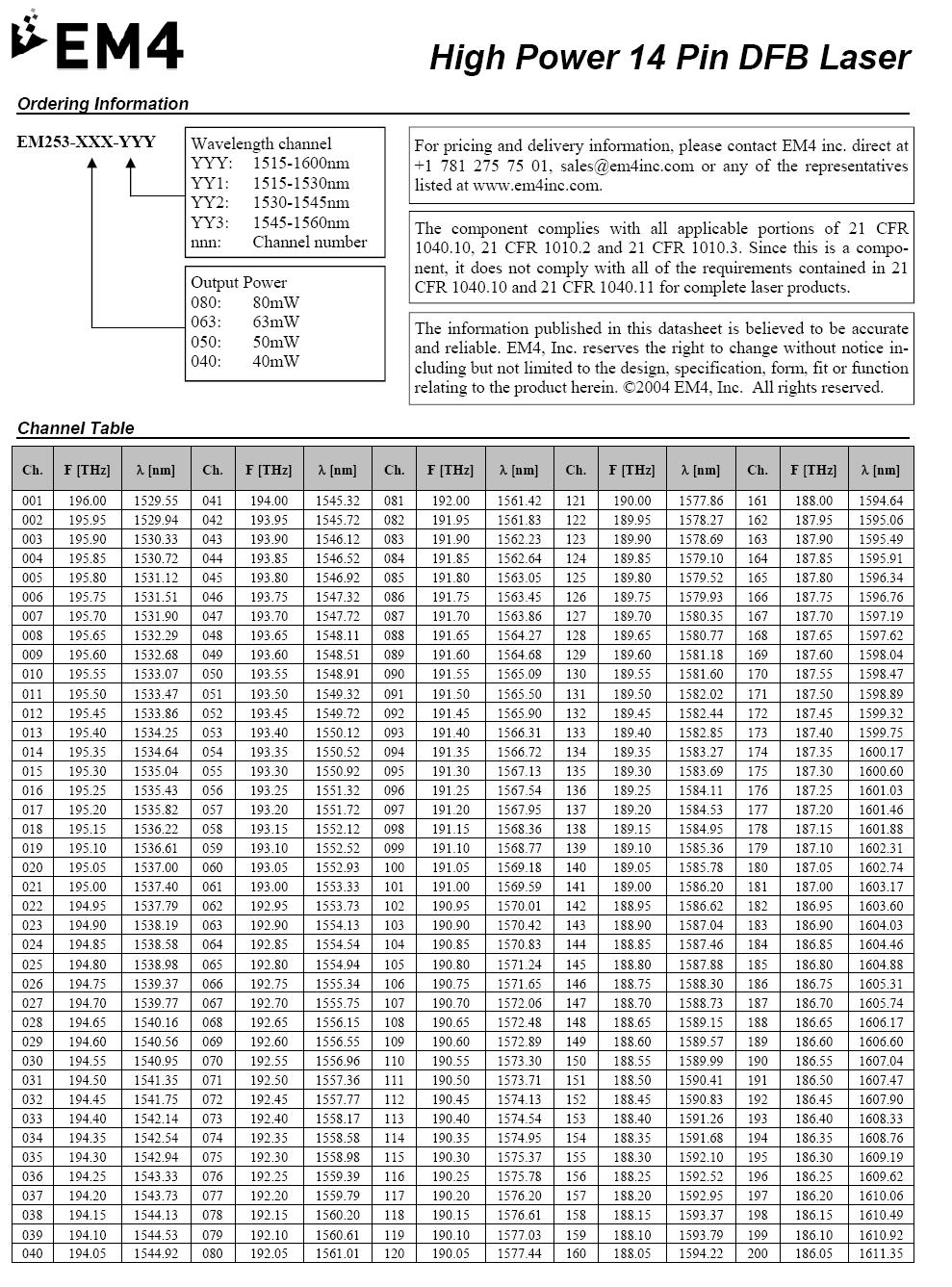
39 III. CHARACTERIZATION OF DFB LASER AND MZI A. DISTRIBUTED FEEDBACK LASER DIODE The EM4 (part number EM ) high power DFB is a CW InGaAsP/InP multi-quantum well (MQW) laser diode. The module is ideal in applications where high power, low input resistance and stable polarization maintaining (PM) fiber properties are needed. The laser diode is housed within an integrated circuit (IC) of the butterfly configuration which also contains a monitor photodiode, thermistor, and inputs for a thermo-electric cooler (TEC). For more information on the EM4 DFB laser a datasheet can be found in Appendix B. The first parameter needed for the simulation of the DFB laser was the peak wavelength of the laser output. The specifications of the laser state the wavelength to be 1550nm. This parameter was confirmed in the laboratory using an optical spectrum analyzer. Figure 6 shows the spectrum of the laser output, the x-axis is in (nm) and the wavelength λ is shown to be nm. Figure 6. Optical Spectrum of the DFB Laser Output. 21
40 In order to verify the maximum optical output power of the DFB laser. The output power was measured by gradually increasing the input drive current of the laser and tabulating the output power of the laser diode. The output connector of the laser was connected to a photodetector that was connected to an digital multi-meter. The photodetector converts light energy to electric power. Thus, the output of the photodetector was displayed on a digital multi-meter. A plot of the tabulated results, optical output power versus drive current, is shown in Figure 7. These values are within the expected range of the laser based on the manufacturer s specifications. 90 DFB Laser Diode Output Power Optical Output Power (mw) Measured Power Drive Current (ma) Figure 7. DFB Laser Diode Optical Output Power versus Drive Current. The next key parameter needed for proper simulation of the laser was the full width half maximum (FWHM) frequency linewidth, Δν. The linewidth of a DFB diode laser is generally too narrow to measure directly using an optical spectrum analyzer. Instead this parameter is measured indirectly using an RF spectrum analyzer. The setup for this measurement is shown in Figure 8. 22
41 Figure 8. Block Diagram of Delayed Self Heterodyning Interferometer Linewidth Measurement Technique. The CW output of the DFB laser is input to 3dB optical beam splitter with one path fed through a long fiber delay (4000m) and the other fed through a lithium niobate (LiNbO3) travelling wave phase modulator. The two paths are recombined (50/50) and then fed to a high-speed photodetector. The electronic output of the photodetector is fed to an RF spectrum analyzer which displays a power spectrum of the interfering waves. The FWHM of this power spectrum is equivalent to the spectral linewidth of the laser. The power spectrum represents a Lorentzian distribution of the photons undergoing spontaneous emission inside the laser, which is the principle cause of linewidth broadening in a laser [1]. The set-up shown in Figure 8 is known as a delayed self heterodyning interferometer (DSHI). Numerous other examples of this measurement technique may be found in the scientific literature [11], [16]. The phase modulator as shown in Figure 8 is used to inject a high frequency component onto the optical carrier to enable the power spectrum to be shifted away from DC, where the FWHM cannot be accurately measured. In the measurements described here, the phase modulator was supplied a 20MHz sinusoid. The long delay is chosen to be larger than the expected value of coherence length, such that delay time is much 23
42 greater than the coherence time ( τ τ ) d c [1]. This ensures the delayed waves at the input of the combiner are uncorrelated with the direct waves. A linewidth measurement is illustrated in Figure 9. From Figure 9 it can be seen that the measured FWHM frequency linewidth was 130kHz for the DFB laser. The video trace of the spectrum analyzer was averaged over 999 samples and applied over a span of 10MHz. Resolution, video bandwidth, and sweep time was all automatically configured. Figure 9. Linewidth measurement using DSHI technique as displayed on RF Spectrum Analyzer. B. MACH-ZEHNDER INTERFEROMETERS Three MZIs are used in the ΣΔ modulator architecture illustrated in Figure 3. In the architecture, the first MZI functions as an analog intensity modulator (AIM) and is used to externally switch the CW laser on and off. The other two MZIs function as Mach- Zehnder Modulators (MZMs) and are used to modulate the sampled RF signal. 24
43 The first characteristic parameter needed for simulation of the MZIs is the voltage required to drive the signal from its minimum to its maximum value. This voltage swing is refer to as V π. The second characteristic is the ability of the MZI to pulse the CW laser. This is a critical step in the ΣΔ modulation process as pulsing the laser is required to sample the incoming RF signal. This is referred to as the on-off extinction ratio of the modulator. The third characterization of the MZIs was done by applying a DC bias voltage to the magnitude and direction components of the RF signal in order to achieve the desired transmissivity. The bias configuration for the MZI # 2, the direction quantization, is preset. Bias configuration of MZI # 3 requires shifting by V π 2 for magnitude quantization. Table 2 shows the characteristics of the three MZIs. For a detailed explanation of the characterization process of the MZIs used in the laboratory, refer to [17]. 25
44 Table 2. MZIs Characterization Parameters. C. SUMMARY The characterization of the DFB laser diode and the MZIs were successfully gathered experimentally. The results were vital for the simulation of the front-end electro-optical ΣΔ modulator presented in the next chapter. 26
45 IV. PHOTONICS OPTSIM SIMULATION A. OVERVIEW This chapter presents a pulse to pulse simulation of an oversampling integrated optical first-order single-bit ΣΔ modulator in OptSim. The electro-optical ΣΔ modulator uses an externally modulated pulsed laser to oversample an input at two MZIs. OptSim is proprietary software of Rsoft Design Group. The simulation package is used to design optical systems, simulate the results, and to compare the performance of the system given various hardware component parameters. The simulation software is used to design and simulate the ΣΔ system by using an interconnected set of blocks. Given various hardware component parameters each block represents a component or subsystem in the ΣΔ system. B. DISTRIBUTED FEEDBACK LASER Semiconductor lasers are quickly becoming the laser of choice for low power applications because of their small size and solid-state construction. The DFB laser used in the laboratory is a high power CW laser diode constructed out of InGaAsP/InP alloy semiconductor material system. With an output power of 80mW and a wavelength of approximately 1550nm this laser was used in conjunction with an analog intensity modulator (AIM) to externally switch the laser off and on. In laboratory experiments the laser linewidth was found by using a delayed self heterodyning method in which the FWHM frequency linewidth was 130kHz. A detailed explanation of the self heterodyning method is found in [16]. In the OptSim simulation software the laser model used was a simplified CW laser. Laser phase noise is taking into account by generating a Lorentzian emission line shape whose FWHM is specified by the parameters and chosen to be 130kHz as measured in the laboratory experiment. Figure 10 shows the parameter list for the CW laser model used in OptSim. The CW power was specified in the model to be 80mW 27
 to switch the laser on and off.")

46 which corresponds to the specification of the laser. Two options are available for laser phase noise bandwidth, ideal which has infinite bandwidth, and realistic bandwidth limited. Ideal was chosen for the model. Figure 10. CW Laser Model and Parameter List. C. ANALOG INTENSITY MODULATOR The CW laser pulses were externally modulated by an analog intensity modular (AIM) to switch the laser on and off. The AIM used for the simulation represents an MZI that consists of a 3dB optical beam intensity splitter, two optical fiber waveguides, electrodes, and an intensity combiner. Figure 4 shows a general schematic diagram of an MZI. The component model implements a single arm Mach-Zehnder amplitude modulator with sin 2 electrical shaped input-output characteristics. The transfer function is typical for a Mach-Zehnder external modulator based on the electro-optic effects in the LiNbO 3 devices. Basic attributes of MZI could be chosen such as on-off extinction ratio, excess loss, transmissivity offset voltage and the value for V π. The value for V π determines the voltage swing needed to switch over between the minimum and maximum 28
![transmission states as represented by equation (14). Figure 11 depicts the parameter list of the AIM-MZI as presented by the simulation software [18]. Figure 11. Parameter Section of the AIM-MZI.](/docs-images/79/78844526/images/47-0.jpg "In order to confirm the functionality of the AIM-MZI model, in particular the V π parameter a 5MHz sawtooth wave signal was positioned as the RF electrical signal input V in to the MZI and used to")
47 transmission states as represented by equation (14). Figure 11 depicts the parameter list of the AIM-MZI as presented by the simulation software [18]. Figure 11. Parameter Section of the AIM-MZI. In order to confirm the functionality of the AIM-MZI model, in particular the V π parameter a 5MHz sawtooth wave signal was positioned as the RF electrical signal input V in to the MZI and used to modulate the CW laser optical signal. The modulated optical signal at the output of the AIM-MZI was observed in order to verify that the modulator indeed had a voltage swing of V π needed to switch over between minimum and maximum transmission states. When the semi-difference between input voltages V in is equal to V on, the power of the optical signal is attenuated by the excess loss only, so the modulator is in the maximum transmission state. To switch to the minimum transmission state a V π voltage must be added or subtracted to V on. Figures 12 and 13 show a pictorial explanation of the transmissivity characteristics and the OptSim schematic used to verify that the AIM-MZI used indeed produced a v π shift, respectively. 29
48 Figure 12. Transmissivity characteristic of the device. Figure 13. OptSim schematic diagram developed for V π confirmation. 30
49 D. MACH-ZEHNDER INTERFEROMETERS Once the external modulation of the DFB laser was correctly achieved by the model, a 5MHz square wave pulse signal with a 20% duty cycle replaced the sawtooth waveform as the electrical RF input to the AIM. Direction and magnitude MZI were added at the output of the AIM with an optical splitter. The optical splitter component implements a balanced splitter with the same attenuation on each output. A simulated RF input (triangle waveform) of 20kHz with amplitude of 3V was added to the electrical input of both the magnitude and direction MZIs. The 3V amplitude matched the 3V ( V π ) inserted into the parameter list of the MZIs. A DC bias of 1.5V ( V π 2) was added to the electrical input of the magnitude MZI for magnitude quantization. Since the direction MZI is already preset for direction quantization there was no need to insert a bias into the direction MZI. In the model shown in Figure 14 the parameters for both direction and magnitude MZI were identical, replicating similar findings in the laboratory experiment. Figure 14. OptSim system simulation schematic. 31
 o ( khz) where f s is the RF antenna sampling frequency and f 0 is the signal bandwidth being sampled at the Nyquist rate.")
50 Since one of the advantages of this type of architecture is being able to oversample wide-band signals directly at the antenna. The OSR was calculated as fs 5MHz OSR = 125 2f = 2 20 = (20) o ( khz) where f s is the RF antenna sampling frequency and f 0 is the signal bandwidth being sampled at the Nyquist rate. Figure 15 shows the direction MZI output waveform depicting 25 samples per division given a total of 125 samples which matches the experimental results. Figure 15. Direction MZI output waveform. The intensity transfer function for both the direction and magnitude MZIs are shown in Figure 16. These results compare rather well to the laboratory results shown in Figure
 Directional MZI, and (b)")
51 Figure 16. Transmissivity Function output waveforms of (a) Directional MZI, and (b) Magnitude MZI. Figure 17. Laboratory Results of Transmissivity Function. 33
52 E. OPTICAL BEAM SPLITTER This component simulates an ideal optical splitter. The component implements a balanced splitter with the same attenuation on each output. To better mimic the real component used in the laboratory a 3dB attenuation loss was inserted on each output parameter. F. PHOTODETECTOR The OptSim model used to implement the photodetector was a PIN photodiode. As stated in chapter II, the photodetector converts photons to electric current (optical input, electrical output). The electrical output is then connected to a simulated electrical oscilloscope which displays the outputs of the MZIs. The photodiode finite bandwidth was modeled using a single-pole transfer function of -3dB bandwidth. The filtering parameter was turned off allowing the device to have ideally an infinite bandwidth. G. SUMMARY The OptSim simulation results show the phase coherent nature of the MZIs. The MZI characteristics were also evaluated with the software model design. In order to compare the performance of the laboratory equipment a simulation was developed to verify the voltage required by the MZI to drive the signal from its minimum to maximum value. This was accomplished by externally modulating an AIM-MZI with a simulated RF signal source. The results confirmed the performance of the MZI model provided by OptSim. Due to limitations in the capabilities of modeling the ring resonator, the model was only developed to the output of the directional and magnitude MZI arms. The results were compared to the laboratory experiments. Utilizing a CW laser pulse model, signal generator sawtooth model, and an AIM model the laser pulse was used to externally modulate the two arms of the MZIs. In this configuration the laser pulse was able to be switched on and off. The voltage swing needed to switch between transmission states was confirmed. All simulation results confirm the correct operation of the integrated optical model in comparison to the laboratory test results. 34
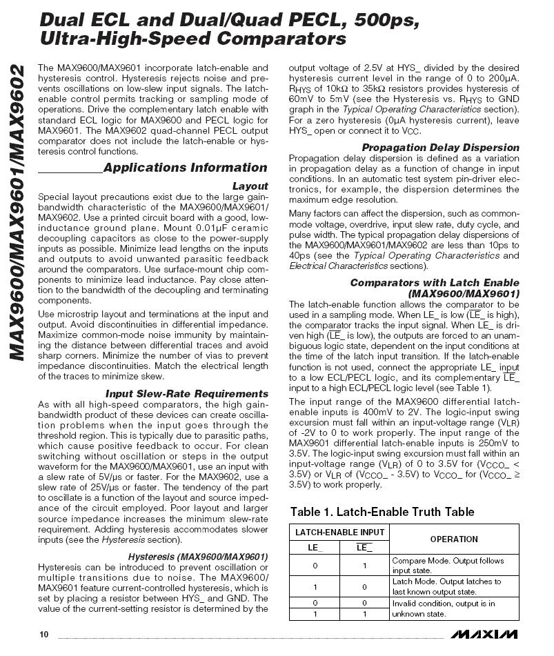
53 V. COMPARATOR PROCESSOR CIRCUIT SIMULATION A. COMPARATOR PROCESSOR CIRCUIT DESIGN The ΣΔ ADC diagram shown in Figure 3 depicts two comparator processor circuits in the diagram. One comparator processor is located after the directional MZI and it delivers an appropriate voltage, σ, to an input of the ring resonator. The second comparator processor circuit is designed to quantize a signal in the loop and provide the output of the modulator. The architecture of the two comparators are the same, the only difference are the inputs and threshold levels. The architecture model consists of two high-speed comparators, nor gates, and a set-reset (S-R) latch, as shown in Figure 18. The circuit was modeled in SmartSpice an analog circuit simulator by SIMUCAD. A spice macromodel of the MAX9602 comparator was obtained from Maxim Integrated Products. The comparator model simulates a dual positive emitter coupled logic (PECL) featuring extremely low propagation delay (500ps). PECL is nothing more than standard emitter coupled logic (ECL) devices run off of a positive power supply [19]. In addition to the comparators, nor gates were modeled using switches and a first order resistor-capacitor (RC) circuit, as shown in Figure 19. The nor gates were designed to operate in the PECL transition region and provide edge detection to the circuit. An S-R latch was designed with two crosscoupled nor gates providing stability of the signal. 35
54 Figure 18. Schematic of Comparator Processor Circuit Design. Figure 19. Schematic of 4-Input NOR Gate Model. 36
55 The high-speed comparator processor design is a proof of concept model of mixed signals architecture. A spice model netlist was developed and is displayed in appendix A. The spice model netlist are organized as a group of subcircuits. In each subcircuit model netlist, the model name is followed by a list of node interconnects. The input of the comparator was configured to simulate an input signal with V max equal to 60mV with a noise level V noise at 20mV. The comparator has two threshold levels V th1 set at 50mV and V th2 set to 15mV. The purpose of V th2 is to identify the quantized noise floor and cancel it. If the path voltage, V in, exceeds the threshold value of the comparator circuit, V th1, the output of the circuit is PECL logic high, the output at Q is high, and the latch is said to be in the set state. Otherwise, the latch is said to be in the clear state setting the output of the comparator to Q low. Simulation results are shown in Figure 20. Figure 20 shows the simulated input signal with threshold levels V th1 and V th2, as well as, the true Q output of the comparator circuit showing the latch in set and reset states. 37
56 Figure 20. (a) Input Signal with Voltage Thresholds Waveform, and (b) Comparator Processor Output waveforms. B. SUMMARY The construction of a high-speed comparator processor circuit has been demonstrated with promising results. A simulated input signal was constructed with a replicated noise floor and the signal was injected into the comparator. Two threshold voltage levels were set for the input signal. One threshold level is designed to identify the input signal, and the other to eliminate the noise in the signal. This comparator circuit serves as a proof of concept model. However, it is not ready to be fully integrated in a 38
57 photonic ΣΔ ADC. In a photonic ΣΔ ADC, a sampling rate of 10 Gsamples/sec (GSPS) would need to be demonstrated. Several papers produced by the Air Force Research Laboratory (AFRL) [13], [20] suggest that an indium phosphide (InP) hetero-junction bipolar transistor (HBT) technology would need to be demonstrated for an on-chip integrated circuit design. 39
58 THIS PAGE INTENTIONALLY LEFT BLANK 40
59 VI. CONCLUSION, LIMITATIONS, AND RECOMMENDATIONS A. CONCLUSION The coherency of the optical ΣΔ ADC design was simulated. A working reliable computer model was developed using RSoft OptSim, an optical circuit simulator. The results confirm the correct operation of the MZIs, transmissivity characteristics, and functionally for future integration. Additionally, the simulation showed the capability to oversample a signal directly at the antenna. A dual comparator circuit with signal and noise threshold levels was simulated for proper operation in the presences of an input signal with a noise floor. In the ΣΔ modulator design the comparator will be able to take signals from the directional MZI or from the output of the ring resonator accumulator. The comparator processor circuit design worked properly with a simulated input, a high-speed comparator model, and generic switching nor gate S-R latch circuit. However, the comparator processer circuit does not operate fast enough for the high sampling rates that are the ultimate goal of this project. In conclusion, it is noteworthy to state that photonics is by nature wideband (THz) and well suited for high-speed signal conversion. Specifically, photonic ADCs have the advantage of precise sampling times, narrow optical sampling apertures, and the ability to sample without contaminating the incident signal. Signal sampling with optical pulses could eliminate the need for a sample and hold circuit, performance limiting components in conventional high-speed ADCs [3]. These factors make photonic ΣΔ ADCs a promising fit in digital receiver systems. B. LIMITATIONS Although the computer models were successful, certain parameters associated with the realities of this type of device were not addressed or simulated. These include signal losses associated with the optical fiber and components, undesired crosstalk within 41
60 the directional couplers, laser jitter, and the length of optical fiber required to affect the proper optical delay within the ring resonator accumulator. The ring resonator design is still an ongoing process as is integration of that device with the ΣΔ system. This thesis, demonstrated that photonics has many attributes that can impact and enhance the performance of high-speed ADCs. Conceptually, a problem with ΣΔ modulator based ADCs is the oversampling requirement, that is, the circuitry of the ADC must be designed to operate at a significantly higher frequency than the maximum frequency of the analog signal that is converted by the ADC. The greater the required accuracy of the ΣΔ modulator ADC, the larger the sampling frequency must be. Limitations in circuit capabilities have, therefore, limited the use of the single channel ΣΔ ADCs to relatively low signal frequencies. However, as one source suggests [4], the sampling frequency may be reduced by using multiple ΣΔ modulators. In addition, the single bit electro-optical ΣΔ modulator depicted in Figure 3 is designed for wide-band sampling frequency signals. This thesis focused on evaluating the wide-band system in narrow-band. C. RECOMMENDATIONS Further efforts include the continued optimization of the first order integrated optical model, by expanding the architecture to withstand the ring resonator architecture. Once the ring resonator is introduced into the setup, precision delay devices may be required to match the optical path lengths for the two interferometers. Another introduction to the photonic architectures would have to be a mode-locked fiber laser with stable femto-second pulses as a timing reference. The mode-locked laser can overcome the timing jitter presented in the sampling apertures of the ADCs. Additionally, signal analysis needs to be modeled and conducted on the oversampled optical ΣΔ outputs at various oversampling ratios to show the increased signal to noise ratio and bit resolution obtained using the decimation filter. A more thorough wide-band analysis needs to be conducted on the entire ΣΔ ADC architecture. 42
61 APPENDIX A. SMARTSPICE SIMULATION SCRIPT MAX9602 SPICE MACROMODEL This section of Appendix A shows the Spice Macromodel for the MAX9602 highspeed comparator. *MAX9602 MACROMODEL * * Revision 0, 11/2003 * * MAX9602 is a ultra-high-speed quad comparator with extremely low * propogation delay(500 ps). The outputs are complimentary digital * signals, compatible with PECL systems. * * Connections * 1 = INA+ * 2 = INA- * 3 = VEE * 4 = INB+ * 5 = INB- * 6 = VCC * 7 = INC+ * 8 = INC- * 9 = VEE * 10 = IND+ * 11 = IND- * 12 = VCC * 13 = QD_ * 14 = QD * 15 = VCCOD * 16 = QC_ * 17 = QC 43
62 * 18 = VCCOC * 19 = QB_ * 20 = QB * 21 = VCCOB * 22 = QA_ * 23 = QA * 24 = VCCOA ***************** * NOTE1: OUT_ IS ACTUALLY COMPLIMENTED OUT. * NOTE2: OUTPUT IS MEASURED WITH RESPECT TO VCC0 * NOTE3: INCLUDE *.OPTIONS ITL4=50 * TO ENHANCE CONVERGENCE. ***************** ****************************************.SUBCKT MAX X MAX9602CMP X MAX9602CMP X MAX9602CMP X MAX9602CMP.ENDS **************************************** *****************.SUBCKT MAX9602CMP *INPUT STAGE **************** RPC RPE **************** CIN 2 5 2P **************** VOS M **************** IEE U Q QX Q QY RC RC **************** *INTERMEDIATE STAGE GA RA K CA E-18 D DX VOH D DX VOL ************** EOUT ************** ECCL EEEL
63 M PMOS M NMOS ************** *DELAY,RISE AND FALL TIME EDELQ T1Q ZO=50 TD=166P RTERMQ CTERMQ P GRISEQ M RRISEQ K C P **** EDELQB T1QB ZO=50 TD=166P RTERMQB CTERMQB P GRISEQB M RRISEQB K C P **************** E E **************** *MODELS USED.MODEL QX PNP(BF=34.188).MODEL QY PNP(BF=32.52).MODEL DX D(N=0.001 TT=1E-15).MODEL NMOS NMOS(KP=1 TOX=100U VTO=0.39 W=1U L=1U).MODEL PMOS PMOS(KP=1 TOX=100U VTO=-0.39 W=1U L=1U) ****************.ENDS **************** 45
64 COMPARATOR PROCESSOR SPICE MODEL SCRIPT This section of the Appendix A shows the Spice simulation script developed for the comparator circuit design. Comparator/NOR gates/sr Flip-Flops * Included Files.INCLUDE MAX9602.txt *Voltage Controlled Switch model statement.model pull_up_sw sw (vt= ron= 1G roff=1) *ECL NOR gate subcircuit.subckt nor2 Vcc Gnd In1 In2 In3 In4 Out r1 Vcc s In1 Gnd pull_up_sw s In2 Gnd pull_up_sw s In3 Gnd pull_up_sw s4 40 Out In4 Gnd pull_up_sw r2 Vcc Out c1 In1 Gnd 4pf c2 In2 Gnd 4pf c3 In3 Gnd 4pf c4 In4 Gnd 4pf c5 Out Gnd 1pf.ends nor2 **Main Circuit** *DC supplies: Comparators/NOR gate VCC Vcc Gnd DC +5.0 VEE Vee Gnd DC -5.2 VCCO Vcco Gnd DC +5.0 Vterm Vtt Gnd DC +3.0 Vinlow Vil Gnd DC *Input Signal Source V1 V2 td tr tf PW T *Vinput In Gnd DC 0.0 PULSE( p 380p 380p 1000p 2760p) Vinput In Gnd DC 0.0 PWL(1ps 0mV ps 20mV 2.0ns 20mV ns 0mV 4ns 0mV ns 60mV 6.0ns 60mV ns 0mV + 8.0ns 0mV ns 20mV 10.0ns 20mV ns 0mV 12.0ns 0mV ns 60mV 14ns 60mV ns 0mV ns 0mV ns 20mV 18.0ns 20mV ns 0mV 20.0ns 0mV ns 60mV 22.0ns 60mV ns 0mV ) Vref1 Vth1 Gnd DC +50.0mV Vref2 Vth2 Gnd DC +15.0mV *First MAX9602 Comparator * IN+ IN- VCC VEE VCCO Q Qnot X1 In Vth1 Vcc Vee Vcco Q1 Q1not MAX9602CMP 46
65 RLQ1 Q1 Vtt 50 RLQ1not Q1not Vtt 50 *Second MAX9602 Comparator * IN+ IN- VCC VEE VCCO Q Qnot X2 Vth2 In Vcc Vee Vcco Q2 Q2not MAX9602CMP RLQ2 Q2 Vtt 50 RLQ2not Q2not Vtt 50 * NOR gates * Buffer signal with 3 NOR gates in series to make input signal more realistic. * VCC VEE In1 In2 In3 In4 Out xnor1 Vcc Gnd Q2 Vil Vil Vil 10 nor2 r1 10 Vtt 50 xnor2 Vcc Gnd 10 Vil Vil Vil 20 nor2 r2 20 Vtt 50 xnor3 Vcc Gnd 20 Vil Vil Vil 30 nor2 r3 30 Vtt 50 xnor4 Vcc Gnd Q2 30 Vil Vil 40 nor2 r4 40 Vtt 50 *SR Latch (Flip-Flop) *1st NOR gate: Input 1 to Vin, Input 2 to output of 2nd NOR gate, 2 remaining inputs to Vinlow *2nd NOR gate: Input 1 to output of 1st NOR gate, Input 2 to Vin, 2 remaining inputs to Vinlow * VCC VEE In1 In2 In3 In4 Out xset Vcc Gnd Vil Vil 50 nor2 r5 50 Vtt 50 xreset Vcc Gnd Q1 50 Vil Vil 60 nor2 r6 60 Vtt 50 **Analysis Requests**.tran 10ps 30000ps **Output Request**.probe.end 47
66 THIS PAGE INTENTIONALLY LEFT BLANK 48

67 APPENDIX B. DATASHEETS MAX9602 DATASHEET This section of Appendix B consists of a datasheet for the MAX9602 PECL highspeed comparator used to model the comparator circuit. 49
68 50
69 51
70 52
71 53
72 54
73 55
74 56
75 57
76 58
77 59
78 60
79 EM4 DFB LASER DIODE DATASHEET This section of Appendix B consists of the datasheet for the DFB laser diode. 61
80 62
81 63
82 64
NAVAL POSTGRADUATE SCHOOL THESIS
 NAVAL POSTGRADUATE SCHOOL MONTEREY, CALIFORNIA THESIS PERFORMANCE EVALUATION OF PHOTONIC SIGMA DELTA ADCS by Yean Wee Tan December 2010 Thesis Advisor: Second Reader: Phillip E. Pace David C. Jenn Approved
DIAMOND-SHAPED SEMICONDUCTOR RING LASERS FOR ANALOG TO DIGITAL PHOTONIC CONVERTERS
 AFRL-SN-RS-TR-2003-308 Final Technical Report January 2004 DIAMOND-SHAPED SEMICONDUCTOR RING LASERS FOR ANALOG TO DIGITAL PHOTONIC CONVERTERS Binoptics Corporation APPROVED FOR PUBLIC RELEASE; DISTRIBUTION
CHAPTER. delta-sigma modulators 1.0
 CHAPTER 1 CHAPTER Conventional delta-sigma modulators 1.0 This Chapter presents the traditional first- and second-order DSM. The main sources for non-ideal operation are described together with some commonly
Lecture 6 Fiber Optical Communication Lecture 6, Slide 1
 Lecture 6 Optical transmitters Photon processes in light matter interaction Lasers Lasing conditions The rate equations CW operation Modulation response Noise Light emitting diodes (LED) Power Modulation
Frequency Dependent Harmonic Powers in a Modified Uni-Traveling Carrier (MUTC) Photodetector
 Photodetector") Naval Research Laboratory Washington, DC 2375-532 NRL/MR/5651--17-9712 Frequency Dependent Harmonic Powers in a Modified Uni-Traveling Carrier (MUTC) Photodetector Yue Hu University of Maryland Baltimore,
Naval Research Laboratory Washington, DC 2375-532 NRL/MR/5651--17-9712 Frequency Dependent Harmonic Powers in a Modified Uni-Traveling Carrier (MUTC) Photodetector Yue Hu University of Maryland Baltimore,
A NOVEL SCHEME FOR OPTICAL MILLIMETER WAVE GENERATION USING MZM
 A NOVEL SCHEME FOR OPTICAL MILLIMETER WAVE GENERATION USING MZM Poomari S. and Arvind Chakrapani Department of Electronics and Communication Engineering, Karpagam College of Engineering, Coimbatore, Tamil
Lecture 2 Fiber Optical Communication Lecture 2, Slide 1
 Lecture 2 General concepts Digital modulation in general Optical modulation Direct modulation External modulation Modulation formats Differential detection Coherent detection Fiber Optical Communication
R. J. Jones College of Optical Sciences OPTI 511L Fall 2017
 R. J. Jones College of Optical Sciences OPTI 511L Fall 2017 Active Modelocking of a Helium-Neon Laser The generation of short optical pulses is important for a wide variety of applications, from time-resolved
Optical Delay Line Application Note
 1 Optical Delay Line Application Note 1.1 General Optical delay lines system (ODL), incorporates a high performance lasers such as DFBs, optical modulators for high operation frequencies, photodiodes,
MICROWAVE photonics is an interdisciplinary area
 314 JOURNAL OF LIGHTWAVE TECHNOLOGY, VOL. 27, NO. 3, FEBRUARY 1, 2009 Microwave Photonics Jianping Yao, Senior Member, IEEE, Member, OSA (Invited Tutorial) Abstract Broadband and low loss capability of
IREAP. MURI 2001 Review. John Rodgers, T. M. Firestone,V. L. Granatstein, M. Walter
 MURI 2001 Review Experimental Study of EMP Upset Mechanisms in Analog and Digital Circuits John Rodgers, T. M. Firestone,V. L. Granatstein, M. Walter Institute for Research in Electronics and Applied Physics
Optoelectronic Oscillator Topologies based on Resonant Tunneling Diode Fiber Optic Links
 Optoelectronic Oscillator Topologies based on Resonant Tunneling Diode Fiber Optic Links Bruno Romeira* a, José M. L Figueiredo a, Kris Seunarine b, Charles N. Ironside b, a Department of Physics, CEOT,
Optical phase-coherent link between an optical atomic clock. and 1550 nm mode-locked lasers
 Optical phase-coherent link between an optical atomic clock and 1550 nm mode-locked lasers Kevin W. Holman, David J. Jones, Steven T. Cundiff, and Jun Ye* JILA, National Institute of Standards and Technology
Communication using Synchronization of Chaos in Semiconductor Lasers with optoelectronic feedback
 Communication using Synchronization of Chaos in Semiconductor Lasers with optoelectronic feedback S. Tang, L. Illing, J. M. Liu, H. D. I. barbanel and M. B. Kennel Department of Electrical Engineering,
Module 16 : Integrated Optics I
 Module 16 : Integrated Optics I Lecture : Integrated Optics I Objectives In this lecture you will learn the following Introduction Electro-Optic Effect Optical Phase Modulator Optical Amplitude Modulator
Modulation of light. Direct modulation of sources Electro-absorption (EA) modulators
 modulators") Modulation of light Direct modulation of sources Electro-absorption (EA) modulators Why Modulation A communication link is established by transmission of information reliably Optical modulation is embedding
Modulation of light Direct modulation of sources Electro-absorption (EA) modulators Why Modulation A communication link is established by transmission of information reliably Optical modulation is embedding
The electric field for the wave sketched in Fig. 3-1 can be written as
 ELECTROMAGNETIC WAVES Light consists of an electric field and a magnetic field that oscillate at very high rates, of the order of 10 14 Hz. These fields travel in wavelike fashion at very high speeds.
The secondary MZM used to modulate the quadrature phase carrier produces a phase shifted version:
 QAM Receiver 1 OBJECTIVE Build a coherent receiver based on the 90 degree optical hybrid and further investigate the QAM format. 2 PRE-LAB In the Modulation Formats QAM Transmitters laboratory, a method
Table of Contents. Abbrevation Glossary... xvii
 Table of Contents Preface... xiii Abbrevation Glossary... xvii Chapter 1 General Points... 1 1.1. Microwave photonic links... 1 1.2. Link description... 4 1.3. Signal to transmit... 5 1.3.1. Microwave
NAVAL POSTGRADUATE SCHOOL THESIS
 NAVAL POSTGRADUATE SCHOOL MONTEREY, CALIFORNIA THESIS DESIGN AND DEVELOPMENT OF A SINGLE CHANNEL RSNS DIRECTION FINDER by Jessica A. Benveniste March 2009 Thesis Co-Advisors: Phillip E. Pace David C. Jenn
AFRL-RY-WP-TR
 AFRL-RY-WP-TR-2017-0158 SIGNAL IDENTIFICATION AND ISOLATION UTILIZING RADIO FREQUENCY PHOTONICS Preetpaul S. Devgan RF/EO Subsystems Branch Aerospace Components & Subsystems Division SEPTEMBER 2017 Final
Choosing the Best ADC Architecture for Your Application Part 3:
 Choosing the Best ADC Architecture for Your Application Part 3: Hello, my name is Luis Chioye, I am an Applications Engineer with the Texas Instruments Precision Data Converters team. And I am Ryan Callaway,
R. J. Jones Optical Sciences OPTI 511L Fall 2017
 R. J. Jones Optical Sciences OPTI 511L Fall 2017 Semiconductor Lasers (2 weeks) Semiconductor (diode) lasers are by far the most widely used lasers today. Their small size and properties of the light output
DIRECT MODULATION WITH SIDE-MODE INJECTION IN OPTICAL CATV TRANSPORT SYSTEMS
 Progress In Electromagnetics Research Letters, Vol. 11, 73 82, 2009 DIRECT MODULATION WITH SIDE-MODE INJECTION IN OPTICAL CATV TRANSPORT SYSTEMS W.-J. Ho, H.-H. Lu, C.-H. Chang, W.-Y. Lin, and H.-S. Su
Spurious-Mode Suppression in Optoelectronic Oscillators
 Spurious-Mode Suppression in Optoelectronic Oscillators Olukayode Okusaga and Eric Adles and Weimin Zhou U.S. Army Research Laboratory Adelphi, Maryland 20783 1197 Email: olukayode.okusaga@us.army.mil
Characteristics of an Optical Delay Line for Radar Testing
 Naval Research Laboratory Washington, DC 20375-5320 NRL/MR/5306--16-9654 Characteristics of an Optical Delay Line for Radar Testing Mai T. Ngo AEGIS Coordinator Office Radar Division Jimmy Alatishe SukomalTalapatra
The 34th International Physics Olympiad
 The 34th International Physics Olympiad Taipei, Taiwan Experimental Competition Wednesday, August 6, 2003 Time Available : 5 hours Please Read This First: 1. Use only the pen provided. 2. Use only the
Study of Multiwavelength Fiber Laser in a Highly Nonlinear Fiber
 Study of Multiwavelength Fiber Laser in a Highly Nonlinear Fiber I. H. M. Nadzar 1 and N. A.Awang 1* 1 Faculty of Science, Technology and Human Development, Universiti Tun Hussein Onn Malaysia, Johor,
LASER DIODE MODULATION AND NOISE
 > 5' O ft I o Vi LASER DIODE MODULATION AND NOISE K. Petermann lnstitutfiir Hochfrequenztechnik, Technische Universitdt Berlin Kluwer Academic Publishers i Dordrecht / Boston / London KTK Scientific Publishers
Semiconductor Optoelectronics Prof. M. R. Shenoy Department of Physics Indian Institute of Technology, Delhi
 Semiconductor Optoelectronics Prof. M. R. Shenoy Department of Physics Indian Institute of Technology, Delhi Lecture - 26 Semiconductor Optical Amplifier (SOA) (Refer Slide Time: 00:39) Welcome to this
Summary Last Lecture
 Interleaved ADCs EE47 Lecture 4 Oversampled ADCs Why oversampling? Pulse-count modulation Sigma-delta modulation 1-Bit quantization Quantization error (noise) spectrum SQNR analysis Limit cycle oscillations
Swept Wavelength Testing:
 Application Note 13 Swept Wavelength Testing: Characterizing the Tuning Linearity of Tunable Laser Sources In a swept-wavelength measurement system, the wavelength of a tunable laser source (TLS) is swept
Application Instruction 002. Superluminescent Light Emitting Diodes: Device Fundamentals and Reliability
 I. Introduction II. III. IV. SLED Fundamentals SLED Temperature Performance SLED and Optical Feedback V. Operation Stability, Reliability and Life VI. Summary InPhenix, Inc., 25 N. Mines Road, Livermore,
Frequency Stabilization Using Matched Fabry-Perots as References
 April 1991 LIDS-P-2032 Frequency Stabilization Using Matched s as References Peter C. Li and Pierre A. Humblet Massachusetts Institute of Technology Laboratory for Information and Decision Systems Cambridge,
PERFORMANCE OF PHOTODIGM S DBR SEMICONDUCTOR LASERS FOR PICOSECOND AND NANOSECOND PULSING APPLICATIONS
 PERFORMANCE OF PHOTODIGM S DBR SEMICONDUCTOR LASERS FOR PICOSECOND AND NANOSECOND PULSING APPLICATIONS By Jason O Daniel, Ph.D. TABLE OF CONTENTS 1. Introduction...1 2. Pulse Measurements for Pulse Widths
PHOTONIC INTEGRATED CIRCUITS FOR PHASED-ARRAY BEAMFORMING
 PHOTONIC INTEGRATED CIRCUITS FOR PHASED-ARRAY BEAMFORMING F.E. VAN VLIET J. STULEMEIJER # K.W.BENOIST D.P.H. MAAT # M.K.SMIT # R. VAN DIJK * * TNO Physics and Electronics Laboratory P.O. Box 96864 2509
Frequency Noise Reduction of Integrated Laser Source with On-Chip Optical Feedback
 MITSUBISHI ELECTRIC RESEARCH LABORATORIES http://www.merl.com Frequency Noise Reduction of Integrated Laser Source with On-Chip Optical Feedback Song, B.; Kojima, K.; Pina, S.; Koike-Akino, T.; Wang, B.;
Optical generation of frequency stable mm-wave radiation using diode laser pumped Nd:YAG lasers
 Optical generation of frequency stable mm-wave radiation using diode laser pumped Nd:YAG lasers T. Day and R. A. Marsland New Focus Inc. 340 Pioneer Way Mountain View CA 94041 (415) 961-2108 R. L. Byer
Electro-optic Electric Field Sensor Utilizing Ti:LiNbO 3 Symmetric Mach-Zehnder Interferometers
 Journal of the Optical Society of Korea Vol. 16, No. 1, March 2012, pp. 47-52 DOI: http://dx.doi.org/10.3807/josk.2012.16.1.047 Electro-optic Electric Field Sensor Utilizing Ti:LiNbO 3 Symmetric Mach-Zehnder
Analysis of Photonic Phase-Shifting Technique Employing Amplitude- Controlled Fiber-Optic Delay Lines
 Naval Research Laboratory Washington, DC 20375-5320 NRL/MR/5650--12-9376 Analysis of Photonic Phase-Shifting Technique Employing Amplitude- Controlled Fiber-Optic Delay Lines Meredith N. Draa Vincent J.
Fiber-Optic Communication Systems
 Fiber-Optic Communication Systems Second Edition GOVIND P. AGRAWAL The Institute of Optics University of Rochester Rochester, NY A WILEY-iNTERSCIENCE PUBLICATION JOHN WILEY & SONS, INC. NEW YORK / CHICHESTER
SUPPLEMENTARY INFORMATION DOI: /NPHOTON
 Supplementary Methods and Data 1. Apparatus Design The time-of-flight measurement apparatus built in this study is shown in Supplementary Figure 1. An erbium-doped femtosecond fibre oscillator (C-Fiber,
3 General Principles of Operation of the S7500 Laser
 Application Note AN-2095 Controlling the S7500 CW Tunable Laser 1 Introduction This document explains the general principles of operation of Finisar s S7500 tunable laser. It provides a high-level description
EXAMINATION FOR THE DEGREE OF B.E. and M.E. Semester
 EXAMINATION FOR THE DEGREE OF B.E. and M.E. Semester 2 2009 101908 OPTICAL COMMUNICATION ENGINEERING (Elec Eng 4041) 105302 SPECIAL STUDIES IN MARINE ENGINEERING (Elec Eng 7072) Official Reading Time:
CHAPTER 5 FINE-TUNING OF AN ECDL WITH AN INTRACAVITY LIQUID CRYSTAL ELEMENT
 CHAPTER 5 FINE-TUNING OF AN ECDL WITH AN INTRACAVITY LIQUID CRYSTAL ELEMENT In this chapter, the experimental results for fine-tuning of the laser wavelength with an intracavity liquid crystal element
Wavelength Control and Locking with Sub-MHz Precision
 Wavelength Control and Locking with Sub-MHz Precision A PZT actuator on one of the resonator mirrors enables the Verdi output wavelength to be rapidly tuned over a range of several GHz or tightly locked
Fibre Optic Sensors: basic principles and most common applications
 SMR 1829-21 Winter College on Fibre Optics, Fibre Lasers and Sensors 12-23 February 2007 Fibre Optic Sensors: basic principles and most common applications (PART 2) Hypolito José Kalinowski Federal University
LOGARITHMIC PROCESSING APPLIED TO NETWORK POWER MONITORING
 ARITHMIC PROCESSING APPLIED TO NETWORK POWER MONITORING Eric J Newman Sr. Applications Engineer in the Advanced Linear Products Division, Analog Devices, Inc., email: eric.newman@analog.com Optical power
NAVAL POSTGRADUATE SCHOOL
 NPS-EC-12-001 NAVAL POSTGRADUATE SCHOOL MONTEREY, CALIFORNIA TOWARDS A NARROWBAND PHOTONIC SIGMA-DELTA DIGITAL ANTENNA by Darren J. Bachmann Phillip E. Pace 1 February 2012 Approved for public release;
Telecommunication Electronics
 Politecnico di Torino ICT School Telecommunication Electronics C5 - Special A/D converters» Logarithmic conversion» Approximation, A and µ laws» Differential converters» Oversampling, noise shaping Logarithmic
Integrated-optical modulators
 LASERS & MATERIAL PROCESSING I OPTICAL SYSTEMS I INDUSTRIAL METROLOGY I TRAFFIC SOLUTIONS I DEFENSE & CIVIL SYSTEMS Integrated-optical modulators Technical information and instructions for use Optoelectronic
Examination Optoelectronic Communication Technology. April 11, Name: Student ID number: OCT1 1: OCT 2: OCT 3: OCT 4: Total: Grade:
 Examination Optoelectronic Communication Technology April, 26 Name: Student ID number: OCT : OCT 2: OCT 3: OCT 4: Total: Grade: Declaration of Consent I hereby agree to have my exam results published on
PSEUDO-RANDOM CODE CORRELATOR TIMING ERRORS DUE TO MULTIPLE REFLECTIONS IN TRANSMISSION LINES
 30th Annual Precise Time and Time Interval (PTTI) Meeting PSEUDO-RANDOM CODE CORRELATOR TIMING ERRORS DUE TO MULTIPLE REFLECTIONS IN TRANSMISSION LINES F. G. Ascarrunz*, T. E. Parkert, and S. R. Jeffertst
The Fundamentals of Mixed Signal Testing
 The Fundamentals of Mixed Signal Testing Course Information The Fundamentals of Mixed Signal Testing course is designed to provide the foundation of knowledge that is required for testing modern mixed
Chapter 1. Overview. 1.1 Introduction
 1 Chapter 1 Overview 1.1 Introduction The modulation of the intensity of optical waves has been extensively studied over the past few decades and forms the basis of almost all of the information applications
System on a Chip. Prof. Dr. Michael Kraft
 System on a Chip Prof. Dr. Michael Kraft Lecture 5: Data Conversion ADC Background/Theory Examples Background Physical systems are typically analogue To apply digital signal processing, the analogue signal
Comparison of FMCW-LiDAR system with optical- and electricaldomain swept light sources toward self-driving mobility application
 P1 Napat J.Jitcharoenchai Comparison of FMCW-LiDAR system with optical- and electricaldomain swept light sources toward self-driving mobility application Napat J.Jitcharoenchai, Nobuhiko Nishiyama, Tomohiro
ModBox Pulse Generation Unit
 ModBox Pulse Generation Unit The ModBox Family The ModBox systems are a family of turnkey optical transmitters and external modulation benchtop units for digital and analog transmission, pulsed and other
Analogical chromatic dispersion compensation
 Chapter 2 Analogical chromatic dispersion compensation 2.1. Introduction In the last chapter the most important techniques to compensate chromatic dispersion have been shown. Optical techniques are able
QAM Transmitter 1 OBJECTIVE 2 PRE-LAB. Investigate the method for measuring the BER accurately and the distortions present in coherent modulators.
 QAM Transmitter 1 OBJECTIVE Investigate the method for measuring the BER accurately and the distortions present in coherent modulators. 2 PRE-LAB The goal of optical communication systems is to transmit
Lecture 4 INTEGRATED PHOTONICS
 Lecture 4 INTEGRATED PHOTONICS What is photonics? Photonic applications use the photon in the same way that electronic applications use the electron. Devices that run on light have a number of advantages
Chapter 3 Experimental study and optimization of OPLLs
 27 Chapter 3 Experimental study and optimization of OPLLs In Chapter 2 I have presented the theory of OPLL and identified critical issues for OPLLs using SCLs. In this chapter I will present the detailed
Absorption: in an OF, the loss of Optical power, resulting from conversion of that power into heat.
 Absorption: in an OF, the loss of Optical power, resulting from conversion of that power into heat. Scattering: The changes in direction of light confined within an OF, occurring due to imperfection in
o Conclusion and future work. 2
 Robert Brown o Concept of stretch processing. o Current procedures to produce linear frequency modulation (LFM) chirps. o How sparse frequency LFM was used for multifrequency stretch processing (MFSP).
DISTRIBUTION A: Distribution approved for public release.
 AFRL-OSR-VA-TR-2014-0205 Optical Materials PARAS PRASAD RESEARCH FOUNDATION OF STATE UNIVERSITY OF NEW YORK THE 05/30/2014 Final Report DISTRIBUTION A: Distribution approved for public release. Air Force
Laser Diode. Photonic Network By Dr. M H Zaidi
 Laser Diode Light emitters are a key element in any fiber optic system. This component converts the electrical signal into a corresponding light signal that can be injected into the fiber. The light emitter
New Features of IEEE Std Digitizing Waveform Recorders
 New Features of IEEE Std 1057-2007 Digitizing Waveform Recorders William B. Boyer 1, Thomas E. Linnenbrink 2, Jerome Blair 3, 1 Chair, Subcommittee on Digital Waveform Recorders Sandia National Laboratories
Fiber Optic Communication Link Design
 Fiber Optic Communication Link Design By Michael J. Fujita, S.K. Ramesh, PhD, Russell L. Tatro Abstract The fundamental building blocks of an optical fiber transmission link are the optical source, the
Analog-to-Digital Converter Survey & Analysis. Bob Walden. (310) Update: July 16,1999
 Update: July 16,1999") Analog-to-Digital Converter Survey & Analysis Update: July 16,1999 References: 1. R.H. Walden, Analog-to-digital converter survey and analysis, IEEE Journal on Selected Areas in Communications, vol. 17,
Analog-to-Digital Converter Survey & Analysis Update: July 16,1999 References: 1. R.H. Walden, Analog-to-digital converter survey and analysis, IEEE Journal on Selected Areas in Communications, vol. 17,
Development of a Low Cost 3x3 Coupler. Mach-Zehnder Interferometric Optical Fibre Vibration. Sensor
 Development of a Low Cost 3x3 Coupler Mach-Zehnder Interferometric Optical Fibre Vibration Sensor Kai Tai Wan Department of Mechanical, Aerospace and Civil Engineering, Brunel University London, UB8 3PH,
Coherent Receivers Principles Downconversion
 Coherent Receivers Principles Downconversion Heterodyne receivers mix signals of different frequency; if two such signals are added together, they beat against each other. The resulting signal contains
All-Optical Signal Processing and Optical Regeneration
 1/36 All-Optical Signal Processing and Optical Regeneration Govind P. Agrawal Institute of Optics University of Rochester Rochester, NY 14627 c 2007 G. P. Agrawal Outline Introduction Major Nonlinear Effects
Using Frequency Diversity to Improve Measurement Speed Roger Dygert MI Technologies, 1125 Satellite Blvd., Suite 100 Suwanee, GA 30024
 Using Frequency Diversity to Improve Measurement Speed Roger Dygert MI Technologies, 1125 Satellite Blvd., Suite 1 Suwanee, GA 324 ABSTRACT Conventional antenna measurement systems use a multiplexer or
The Lightwave Model 142 CW Visible Ring Laser, Beam Splitter, Model ATM- 80A1 Acousto-Optic Modulator, and Fiber Optic Cable Coupler Optics Project
 The Lightwave Model 142 CW Visible Ring Laser, Beam Splitter, Model ATM- 80A1 Acousto-Optic Modulator, and Fiber Optic Cable Coupler Optics Project Stephen W. Jordan Seth Merritt Optics Project PH 464
ECEN689: Special Topics in Optical Interconnects Circuits and Systems Spring 2016
 ECEN689: Special Topics in Optical Interconnects Circuits and Systems Spring 016 Lecture 7: Transmitter Analysis Sam Palermo Analog & Mixed-Signal Center Texas A&M University Optical Modulation Techniques
Setup of the four-wavelength Doppler lidar system with feedback controlled pulse shaping
 Setup of the four-wavelength Doppler lidar system with feedback controlled pulse shaping Albert Töws and Alfred Kurtz Cologne University of Applied Sciences Steinmüllerallee 1, 51643 Gummersbach, Germany
Chapter 10 WDM concepts and components
 Chapter 10 WDM concepts and components - Outline 10.1 Operational principle of WDM 10. Passive Components - The x Fiber Coupler - Scattering Matrix Representation - The x Waveguide Coupler - Mach-Zehnder
Optical Communications and Networking 朱祖勍. Sept. 25, 2017
 Optical Communications and Networking Sept. 25, 2017 Lecture 4: Signal Propagation in Fiber 1 Nonlinear Effects The assumption of linearity may not always be valid. Nonlinear effects are all related to
SHF Communication Technologies AG
 SHF Communication Technologies AG Wilhelm-von-Siemens-Str. 23 Aufgang D 12277 Berlin Marienfelde Germany Phone ++49 30 / 772 05 10 Fax ++49 30 / 753 10 78 E-Mail: sales@shf.biz Web: http://www.shf.biz
EE247 Lecture 26. This lecture is taped on Wed. Nov. 28 th due to conflict of regular class hours with a meeting
 EE47 Lecture 6 This lecture is taped on Wed. Nov. 8 th due to conflict of regular class hours with a meeting Any questions regarding this lecture could be discussed during regular office hours or in class
Investigations on the performance of lidar measurements with different pulse shapes using a multi-channel Doppler lidar system
 Th12 Albert Töws Investigations on the performance of lidar measurements with different pulse shapes using a multi-channel Doppler lidar system Albert Töws and Alfred Kurtz Cologne University of Applied
Holography Transmitter Design Bill Shillue 2000-Oct-03
 Holography Transmitter Design Bill Shillue 2000-Oct-03 Planned Photonic Reference Distribution for Test Interferometer The transmitter for the holography receiver is made up mostly of parts that are already
Lecture 3 Concepts for the Data Communications and Computer Interconnection
 Lecture 3 Concepts for the Data Communications and Computer Interconnection Aim: overview of existing methods and techniques Terms used: -Data entities conveying meaning (of information) -Signals data
1550 nm Programmable Picosecond Laser, PM
 1550 nm Programmable Picosecond Laser, PM The Optilab is a programmable laser that produces picosecond pulses with electrical input pulses. It functions as a seed pulse generator for Master Oscillator
Simultaneous Measurements for Tunable Laser Source Linewidth with Homodyne Detection
 Simultaneous Measurements for Tunable Laser Source Linewidth with Homodyne Detection Adnan H. Ali Technical college / Baghdad- Iraq Tel: 96-4-770-794-8995 E-mail: Adnan_h_ali@yahoo.com Received: April
Photonic Microwave Harmonic Generator driven by an Optoelectronic Ring Oscillator
 Photonic Microwave Harmonic Generator driven by an Optoelectronic Ring Oscillator Margarita Varón Durán, Arnaud Le Kernec, Jean-Claude Mollier MOSE Group SUPAERO, 1 avenue Edouard-Belin, 3155, Toulouse,
Laser Transmitter Adaptive Feedforward Linearization System for Radio over Fiber Applications
 ASEAN IVO Forum 2015 Laser Transmitter Adaptive Feedforward Linearization System for Radio over Fiber Applications Authors: Mr. Neo Yun Sheng Prof. Dr Sevia Mahdaliza Idrus Prof. Dr Mohd Fua ad Rahmat
ECEN689: Special Topics in Optical Interconnects Circuits and Systems Spring 2016
 ECEN689: Special Topics in Optical Interconnects Circuits and Systems Spring 2016 Lecture 9: Mach-Zehnder Modulator Transmitters Sam Palermo Analog & Mixed-Signal Center Texas A&M University Mach-Zehnder
Model Series 400X User s Manual. DC-100 MHz Electro-Optic Phase Modulators
 Model Series 400X User s Manual DC-100 MHz Electro-Optic Phase Modulators 400412 Rev. D 2 Is a registered trademark of New Focus, Inc. Warranty New Focus, Inc. guarantees its products to be free of defects
Introduction Fundamentals of laser Types of lasers Semiconductor lasers
 ECE 5368 Introduction Fundamentals of laser Types of lasers Semiconductor lasers Introduction Fundamentals of laser Types of lasers Semiconductor lasers How many types of lasers? Many many depending on
Chapter 2: Digitization of Sound
 Chapter 2: Digitization of Sound Acoustics pressure waves are converted to electrical signals by use of a microphone. The output signal from the microphone is an analog signal, i.e., a continuous-valued
Suppression of Stimulated Brillouin Scattering
 Suppression of Stimulated Brillouin Scattering 42 2 5 W i de l y T u n a b l e L a s e r T ra n s m i t te r www.lumentum.com Technical Note Introduction This technical note discusses the phenomenon and
is a method of transmitting information from one place to another by sending light through an optical fiber. The light forms an electromagnetic
 is a method of transmitting information from one place to another by sending light through an optical fiber. The light forms an electromagnetic carrier wave that is modulated to carry information. The
CHAPTER 4 RESULTS. 4.1 Introduction
 CHAPTER 4 RESULTS 4.1 Introduction In this chapter focus are given more on WDM system. The results which are obtained mainly from the simulation work are presented. In simulation analysis, the study will
Timing Noise Measurement of High-Repetition-Rate Optical Pulses
 564 Timing Noise Measurement of High-Repetition-Rate Optical Pulses Hidemi Tsuchida National Institute of Advanced Industrial Science and Technology 1-1-1 Umezono, Tsukuba, 305-8568 JAPAN Tel: 81-29-861-5342;
ModBox - Spectral Broadening Unit
 ModBox - Spectral Broadening Unit The ModBox Family The ModBox systems are a family of turnkey optical transmitters and external modulation benchtop units for digital and analog transmission, pulsed and
π code 0 Changchun,130000,China Key Laboratory of National Defense.Changchun,130000,China Keywords:DPSK; CSRZ; atmospheric channel
 4th International Conference on Computer, Mechatronics, Control and Electronic Engineering (ICCMCEE 2015) Differential phase shift keying in the research on the effects of type pattern of space optical
UNIT 2. Q.1) Describe the functioning of standard signal generator. Ans. Electronic Measurements & Instrumentation
 Describe the functioning of standard signal generator. Ans. Electronic Measurements & Instrumentation") UNIT 2 Q.1) Describe the functioning of standard signal generator Ans. STANDARD SIGNAL GENERATOR A standard signal generator produces known and controllable voltages. It is used as power source for the
UNIT 2 Q.1) Describe the functioning of standard signal generator Ans. STANDARD SIGNAL GENERATOR A standard signal generator produces known and controllable voltages. It is used as power source for the
Elements of Optical Networking
 Bruckner Elements of Optical Networking Basics and practice of optical data communication With 217 Figures, 13 Tables and 93 Exercises Translated by Patricia Joliet VIEWEG+ TEUBNER VII Content Preface
MINIATURIZED ANTENNAS FOR COMPACT SOLDIER COMBAT SYSTEMS
 MINIATURIZED ANTENNAS FOR COMPACT SOLDIER COMBAT SYSTEMS Iftekhar O. Mirza 1*, Shouyuan Shi 1, Christian Fazi 2, Joseph N. Mait 2, and Dennis W. Prather 1 1 Department of Electrical and Computer Engineering