BSW MHz-6000MHz High Linearity Reflective SPDT RF switch. Product Description. Package Type. Device Features - Common.
|
|
|
- Janel Rogers
- 6 years ago
- Views:
Transcription


1 Product Description The BSW6321 is a reflective SPDT RF switch that can be used in high power and good performance WiMAX , WLAN a/b/g/n/ac/ax and DOCSIS 3.0/3.1 applications. This device is packaged in RoHS-compliant with 1.5x1.5mm, 6-lead UDFN package. It must be used with back side ground soldering. The BSW6321 has robust ESD protection circuits at all pins and temperature performance (operating temperature range : -40 ~ +105 C), furthermore this switch does not require blocking capacitors. This device also has a high linearity performance over all temperature range such as IIP3, IIP2. A functional block diagram is shown in Figure 1. Block Diagram Package Type 6-Lead 1.5x1.5mm, UDFN Package Figure 2 Package Type Device Features - Common Output frequency range : 5 MHz to 6.0 GHz Supply Voltage : 2.7V to 5.5V ESD protection : all pins 6-lead DFN package : 1.5mm x 1.5mm x 0.5mm Operating temperature range : -40 C C Device Features - 50Ω Applications Figure 1 Functional Block Diagram WiMAX WLAN a/b/g/n/ac/ax DOCSIS 3.0/3.1 Drone NFC Bluetooth Smart Card Wireless Infrastructure Remote keyless entry Telematics / Infotainment Two-way radios Wireless control systems GPS/Navigation Low insertion loss : : High isolation : : Input 1 db output compression (ANT Tx) : : High IIP3 (ANT Tx) : : Device Features - 75Ω Low insertion loss : 204MHz High isolation : 204MHz High IIP3 : 633MHz 2 nd / 3 rd Harmonic : 111dBc / 633MHz 1
2 Electrical Specifications - 50Ω Typical conditions are at VDD = 3.3V, T A = 25 C, V1 Low = 0V, V1 High = 3.3V, Z L = 50Ω, Excluding SMA Connector and PCB loss, unless otherwise Table 1 Electrical Specifications - 50Ω Parameter Path Condition Min Typ Max Unit Operating Frequency MHz 13.56MHz GHz 2GHz Insertion Loss 3GHz 4GHz db 5GHz GHz MHz 82 1GHz 2GHz Isolation 3GHz 4GHz db 5GHz 32 6GHz MHz 82 1GHz 2GHz Tx - Rx 35 Isolation Rx - Tx 3GHz 4GHz db 5GHz 25 6GHz Return Loss ANT, Tx, Rx 5MHz 6GHz (Active port) 20 db Input P1dB dbm * Tone Power is 18dBm and Tone spacing is 20KHz. ** DC transient test at RF all ports (ANT,Tx,Rx) when V1 is switched from High to Low or from Low to High in a 50Ω setup. Excluding SMA Connector and PCB loss. 1GHz (0.12dB), 2GHz (0.20dB), 3GHz (0.27dB), 4GHz (0.35dB), 5GHz (0.51dB), 6GHz (0.52dB) 2
3 Electrical Specifications - 50Ω Typical conditions are at VDD = 3.3V, T A = 25 C, V1 Low = 0V, V1 High = 3.3V, Z L = 50Ω, Excluding SMA Connector and PCB loss, unless otherwise Table 2 Electrical Specifications - 50Ω Parameter Path Condition Min Typ Max Unit Input IP3* dbm Input IP2* dbm 2 nd Harmonic dbc 3 rd Harmonic dbc Video Feedthrough** 5ns rise-time pulse 15 mvpp Switching Time 50% control to 90% RF 50% control to 10% RF ns * Tone Power is 18dBm and Tone spacing is 20KHz. ** DC transient test at RF all ports (ANT,Tx,Rx) when V1 is switched from High to Low or from Low to High in a 50Ω setup. Excluding SMA Connector and PCB loss. 1GHz (0.12dB), 2GHz (0.20dB), 3GHz (0.27dB), 4GHz (0.35dB), 5GHz (0.51dB), 6GHz (0.52dB) 3
4 Electrical Specifications - 75Ω Typical conditions are at VDD = 3.3V, T A = 25 C, V1 Low = 0V, V1 High = 3.3V, Z L = 75Ω, Excluding SMA Connector and PCB loss, unless otherwise Table 3 Electrical Specifications - 75Ω Parameter Path Condition Min Typ Max Unit Operating Frequency MHz 5MHz 0.25 Insertion Loss RFC - RFx 204MHz 1218MHz db 1700MHz MHz MHz 85 Isolation RFC to RFx 204MHz 612MHz db 1218MHz MHz 27 5MHz 85 Isolation RFx to RFx 204MHz 612MHz db 1218MHz 1794MHz Return Loss RFC, RFx 5MHz 3GHz (Active port) db Input P1dB RFC - RFx 50Ω 33 dbm Input IP3* (note) RFC - RFx 633MHz (Pin=18dBm/tone) 72 dbm Input IP2* (note) RFC RFx 633MHz (Pin=18dBm/tone) 110 dbm 2 nd Harmonic RFC RFx 633MHz (Pin=25dBm) 111 dbc 3 rd Harmonic RFC RFx 633MHz (Pin=25dBm) 120 dbc Video Feedthrough** 5ns rise-time pulse 15 mvpp Switching Time RFC RFx 50% control to 90% RF 50% control to 10% RF ns * Tone spacing is 20KHz. ** DC transient test at RF all ports (RFC, RF1, RF2) when V1 is switched from High to Low or from Low to High in a 75Ω setup. Excluding SMA Connector and PCB loss. 5MHz(0.02dB), 204MHz(0.05dB), 1218MHz(0.13dB), 1700MHz(0.17dB), 1794MHz(0.19dB) 4
 Tx RF port (RF1).")
 V1 High 1.0-3.3 V V1 Low 0-0.")
5 Product Description Table 4 Pin Descriptions No. Pin Name Descriptions 1 V1 Digital Control Logic Input. 2 ANT (RFC) ANT RF port (RFC). 3 VDD Supply Voltage. 4 Rx (RF2) Rx RF port (RF2). 5 GND Ground 6 Tx (RF1) Tx RF port (RF1). Figure 3 Functional Block Diagram Pad Exposed Pad Ground Table 5 V1 Control Truth Table V1 ANT-Tx ANT-Rx 0 OFF ON 1 ON OFF Table 6 Operating Ranges Parameter Symbol Min Typ Max Unit Supply Voltage VDD V Supply Current IDD μa Digital Input Control (V1) V1 High V V1 Low V Operating Temperature Range To C Table 7 Absolute Maximum Ratings ESD Parameter Symbol Min Max Unit Supply Voltage VDD V Digital Input Voltage (V1) V V Maximum Input Power dbm Storage Temperature range C HBM All pins V CDM All pins V 5


 Figure 6 Return Loss (RFC, RFx)")
6 Typical Performances - 50Ω Typical conditions are at VDD = 3.3V, T A = 25 C, V1 Low = 0V, V1 High = 3.3V, Z L = 50Ω, Excluding SMA Connector and PCB loss, unless otherwise Figure 4 Insertion Loss vs. Vdd (RFC - RFx) Figure 5 Insertion Loss vs. Temp (RFC - RFx) Figure 6 Return Loss (RFC, RFx) Figure 7 Return Loss vs. Temp (RFC) 6
 Figure 9 Isolation vs.")
7 Typical Performances - 50Ω Typical conditions are at VDD = 3.3V, T A = 25 C, V1 Low = 0V, V1 High = 3.3V, Z L = 50Ω, Excluding SMA Connector and PCB loss, unless otherwise Figure 8 Isolation vs. Vdd (RFC - RFx) Figure 9 Isolation vs. Temp (RFC-RFx) Figure 10 Isolation vs. Vdd (RFx - RFx) Figure 11 Isolation vs. Temp (RFx - RFx) 7

")
 Figure 14 Return Loss (RFC, RFx)")
8 Typical Performances - 75Ω Typical conditions are at VDD = 3.3V, T A = 25 C, V1 Low = 0V, V1 High = 3.3V, Z L = 75Ω, Excluding SMA Connector and PCB loss, unless otherwise Figure 12 Insertion Loss (RFC - RFx) Figure 13 Insertion Loss vs. Temp (RFC - RFx) Figure 14 Return Loss (RFC, RFx) Figure 15 Return Loss vs. Temp (RFC) 8

 Figure 17 Isolation vs.")
9 Typical Performances - 75Ω Typical conditions are at VDD = 3.3V, T A = 25 C, V1 Low = 0V, V1 High = 3.3V, Z L = 75Ω, Excluding SMA Connector and PCB loss, unless otherwise Figure 16 Isolation (RFC - RFx) Figure 17 Isolation vs. Temp (RFC - RFx) Figure 18 Isolation (RFx - RFx) Figure 19 Isolation vs. Temp (RFx - RFx) 9

, Bottom Layer No.")
10 Evaluation Board - 50Ω VDD GND V1 ANT (RFC) Rx (RF2) Tx (RF1) Figure 20 Evaluation Board Layout - 50Ω V1 C6 DNI J5 Tx V1_IN VDD_IN 9 10 ANT J1 1 V1 2 ANT 3 VDD Tx 6 GND 5 Rx 4 V1 2 1 J2 VDD C5 100pF U2 J4 Rx U1 C2 1uF R2 0Ω C4 100pF VDD Figure 21 Evaluation Board Schematic - 50Ω Table 8 Bill of Material - Evaluation Board 50Ω RO4003C Er : 3.38 FR-4 Er : 4.5~4.8 FR-4 Er : 4.5~4.8 COPPER : 1oz (0.035mm), Top Layer RO4003C / 0.305mm COPPER : 1oz (0.035mm), Inner Layer FR-4 / 0.36mm FINISH THICKNESS : 1.55T COPPER : 1oz (0.035mm), Inner Layer FR-4 / 0.73mm COPPER : 1oz (0.035mm), Bottom Layer No. Ref Des Part Qty Part Number Remark 1 C2 1 CAP uF J 50V 2 C4 1 CAP pF J 50V 3 C5* 1 CAP pF J 50V 4 C6 1 CAP 1005 DNI 5 R2 1 RES 1608 J 0ohm 6 U1 1 3 Pin Header 7 J Pin Header Figure 22 Evaluation Board PCB Layer Information 50Ω 8 ANT, Tx, Rx 3 SMA_END_LAUNCH 9 U X1.5_6L_ BSW6321 * C5 should be placed near the device. 10


11 Evaluation Board - 75Ω VDD RFC V1 GND RF2 RF1 Ref Line Figure 23 Evaluation Board Layout - 75Ω V1 C1 DNI SMA3 RF1 VDD_IN J2 C4 1uF VDD RFC SMA1 1 V1 2 RFC 3 VDD RF1 6 GND 5 RF2 4 V1_IN V1 VDD C3 DNI U1 SMA2 RF2 J3 C2 1uF Figure 24 Evaluation Board Schematic - 75Ω Table 9 Bill of Material - Evaluation Board 75Ω FR-4 Er : 4.5~4.8 FR-4 Er : 4.5~4.8 FR-4 Er : 4.5~4.8 COPPER : 1oz (0.035mm), Top Layer FR-4 / 0.58mm COPPER : 1oz (0.035mm), Inner Layer FR-4 / 0.3mm FINISH THICKNESS :1.6T COPPER : 1oz (0.035mm), Inner Layer FR-4 / 0.58mm COPPER : 1oz (0.035mm), Bottom Layer No. Ref Des Part Qty Part Number Remark 1 C2,C4 2 CAP uF 50V 2 C1,C3 2 CAP 0402 DNI 3 RFC,RF1,RF2 3 F Type_END_LAUNCH 4 J2,J3 2 2 Pin Header 5 U2 1 DFN 1.5X1.5_6L_ BSW6321 Figure 25 Evaluation Board PCB Layer Information 75Ω 11


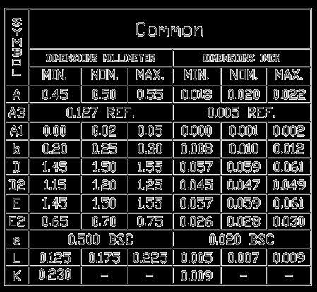
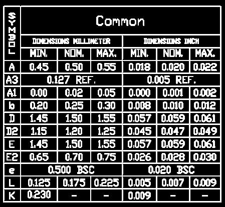
12 Package Outline Drawing Figure 26 Package Outline Drawing Figure 27 Recommended Land Pattern 12
13 Tape & Reel 0.25± ± ± ± ± ± ±0.30 Packaging information : Tape Width (mm) : 8 Reel Size (inches) : 7 Device Cavity Pitch (mm) : 4 Device Per Reel : 3000EA 0.75± ± ±0.05 ø1.00±0.10 Package Marking S : Switch 2 : The number of switch throw B : Sequential Number Y : Year WW : Work Week Figure 28 Package Marking Lead plating finish 100% Tin Matte finish (All BeRex products undergoes a 1 hour, 150 degree C, Anneal bake to eliminate thin whisker growth concerns.) MSL / ESD Rating ESD Rating: Class 2 Value: Passes < 2500V Test: Human Body Model (HBM) Standard: JEDEC Standard JESD22-A114B MSL Rating: Level 1 at +265 C convection reflow Standard: JEDEC Standard J-STD-020 NATO CAGE code: 2 N 9 6 F 13
Preliminary Datasheet
 Product Description The is a reflective SPDT RF switch that can be used in high power and good performance WLAN 802.11 a/b/g/n/ac/ax, DOCSIS 3.0/3.1 and Wireless Communication applications. This device
Preliminary Datasheet
 Product Description The is a reflective SPDT RF switch that can be used in high power and good performance WLAN 802.11 a/b/g/n/ac/ax, DOCSIS 3.0/3.1 and Wireless Communication applications. This device
Preliminary Datasheet
 Product Description The is an absorptive SPDT 50Ω matched RF switch supporting bandwidths up to 6GHz. Its high linearity performance across the temperature range makes it ideally suited for use in 3G/4G/5G
3 OIP3 _ measured with two tones at an output of 9dBm per tone separated by 1 MHz.
 Device Features OIP3 = 36.9dBm @ 950 MHz Gain = 17.1 db @ 950 MHz Output P1 = 19.5 dbm @950 MHz CTB = 80.0 dbc @ 300MHz CTO = 64.0 dbc @ 300MHz Patented temperature compensation Lead-free/RoHS-compliant
Preliminary Datasheet
 Device Features This can be operated at Vd of 3.0V N.F = 0.78 db @ 1850MHz at Demo board 31.5 dbm Output IP3 at 0dBm/tone at 1850MHz 15.6 db Gain at 1850MHz 17.7 dbm P1dB at 1850 MHz Lead-free/Green/RoHS
Typical Performance 1. 1 Device performance _ measured on a BeRex evaluation board at 25 C, 50 Ω system.
 Device Features NF = 0.95 db @ 900MHz at RF connectors of Demo board Gain = 20.5 db @ 900 MHz OIP3 = 30.0 dbm @ 1900MHz Output P1 db = 17.5 dbm @ 900MHz 5V/27mA, MTTF > 100 Years, MSL 1, Class 0 Lead-free/RoHS-compliant
Typical Performance 1. IS-95C ACPR dbm WCDMA ACLR dbm
 Device Features OIP3 = 45.0 dbm @ 1900 MHz Gain = 15.0 db @ 1900 MHz Output P1 db = 27.5 dbm @ 1900 MHz 50 Ω Cascadable Patented Over Voltage Protection Circuit Lead-free/RoHS-compliant SOT-89 SMT package
Preliminary Datasheet
 Product Description Figure 2. Package Type The is a digitally controlled variable gain amplifier (DVGA) is featuring high linearity using the voltage 3V supply with a broadband frequency range of 30 to
Typical Performance 1. Absolute Maximum Ratings. Parameter
 Device Features Typical Isolation = 23 db Typical Insertion Loss = 0.5 db MSL 3 moisture rating Lead-free/RoHS-compliant SOIC-8 Plastic Package With exposed back side ground pad Product Description BeRex
Typical Performance 1. Absolute Maximum Ratings. Parameter
 Device Features Typical Isolation = 23 db Typical Insertion Loss = 0.4 db MSL 3 moisture rating Lead-free/RoHS-compliant SOIC-8 Plastic Package With exposed back side ground pad Product Description BeRex
Typical Performance 1. 1 Device performance _ measured on a BeRex evaluation board at 25 C, 50 Ω system.
 Device Features OIP3 = 43.0 dbm @ 900 MHz Gain = 20.0 db @ 900 MHz Output P1 db = 24.5 dbm @ 900 MHz 50 Ω Cascadable Lead-free/RoHS-compliant SOT-89 SMT package Product Description BeRex s BT09AG is a
Typical Performance 1. 1 Device performance _ measured on a BeRex evaluation board at 25 C, 50 Ω system.
 Device Features OIP3 = 41.0 dbm @ 1900 MHz Gain = 15.5 db @ 1900 MHz Output P1 db = 25.5 dbm @ 1900 MHz 50 Ω Cascadable Lead-free/RoHS-compliant SOT-89 SMT package Product Description BeRex s BT09VG is
Typical Performance 1. 2 OIP3 _ measured on two tones with a output power 23dBm/ tone, F2 F1 = 1 MHz.. Absolute Maximum Ratings
 Device Features +5V/550mA at operating bias condition Gain = 25.5 db @ 2.65 GHz P1dB = 33.5 dbm @ 2.65GHz LTE 10M ACLR = 22.7dBm Output Power at -50dBc @ 2.65GHz Intergrated interstage matching Lead-free/Green/RoHS-compliant
Typical Performance 1. Absolute Maximum Ratings
 Device Features +5V/680mA at operating bias condition Gain = 27.3 db @ 1850 MHz P1dB = 33.1 dbm @ 1850MHz LTE 10M ACLR = 23.5dBm Output Power at -50dBc @ 1850MHz Intergrated interstage matching Lead-free/Green/RoHS-compliant
Preliminary Datasheet
 Product Description Figure 2. Package Type The is a digitally controlled variable gain amplifier (DVGA) in a 6x6mm LGA package, with a frequency range of 4400 to 5000 MHz and an operating Vcc of 5.0V.
Preliminary Datasheet
 BVAB -4 MHz Product Description Figure. Package Type The BVAB is a digitally controlled variable gain amplifier (DVGA) is featuring high linearity using the voltage V supply with a broadband frequency
Preliminary Datasheet
 Product Description Figure 2. Package Type The is a digitally controlled variable gain amplifier (DVGA) is featuring high linearity using the voltage 3.3V supply with a broadband frequency range of 50
Nonreflective, Silicon SP4T Switch, 0.1 GHz to 6.0 GHz HMC7992
 Nonreflective, Silicon SP4T Switch,.1 GHz to 6. GHz FEATURES Nonreflective, 5 Ω design High isolation: 45 db typical at 2 GHz Low insertion loss:.6 db at 2 GHz High power handling 33 dbm through path 27
Preliminary Datasheet
 BVA4B -4 MHz Product Description Figure. Package Type The BVA4B is a digitally controlled variable gain amplifier (DVGA) is featuring high linearity using the voltage.v supply with a broadband frequency
HMC241AQS16 / 241AQS16E
 v00.1213 Typical Applications Features The HMC241AQS16 & HMC241AQS16E are ideal for: Base Stations & Portable Wireless CATV / DBS Wireless Local Loop Test Equipment Functional Diagram RoHS Compliant Product
Features +3V +5V GHz
 Typical Applications The is ideal for: Cellular/4G Infrastructure WiMAX, WiBro & Fixed Wireless Automotive Telematics Mobile Radio Test Equipment Functional Diagram Features High Isolation: up to Single
Features OBSOLETE. Isolation DC GHz db
 Typical Applications Features - 224 The is ideal for: Cellular / 4G Infrastructure WiMAX, WiBro & Fixed Wireless Automotive Telematics Mobile Radio Test Equipment Functional Diagram Input P1dB: + @ Vdd
Typical Performance 1. Absolute Maximum Ratings
 Device Features +5V/215mA at operating bias condition Gain = 16.0 db @ 2400MHz P1dB = 29.5 dbm @ 2400MHz OIP3 = 42.1dBm 16dBm/tone at 2400MHz LTE 20M ACLR = 19.1dBm Output Power at -50dBc @ 2400MHz Lead-free/Green/RoHS-compliant
10 W, Failsafe, GaAs, SPDT Switch 0.2 GHz to 2.7 GHz HMC546LP2E
 FEATURES High input P.dB: 4 dbm Tx Low insertion loss:.4 db High input IP3: 67 dbm Positive control: V low control; 3 V to 8 V high control Failsafe operation: Tx is on when no dc power is applied APPLICATIONS
Features. Parameter Frequency Min. Typ. Max. Units
 v1.6 Typical Applications The HMC545A / HMC545AE is ideal for: Cellular/3G Infrastructure Private Mobile Radio Handsets WLAN, WiMAX & WiBro Automotive Telematics Test Equipment Functional Diagram Features
Features. Parameter Frequency Min. Typ. Max. Units DC GHz DC GHz DC GHz DC GHz DC GHz Isolation DC - 4.
 Typical Applications The is ideal for: Cellular / 4G Infrastructure WiMAX, WiBro & Fixed Wireless Automotive Telematics Mobile Radio Test Equipment Features Input P1: +40 @ Vdd = +8V High Third Order Intercept:
High Isolation, Silicon SPDT, Nonreflective Switch, 0.1 GHz to 6.0 GHz HMC8038W
 5 6 7 8 6 5 4 3 FEATURES Nonreflective, 50 Ω design High isolation: 60 db typical Low insertion loss: 0.8 db typical High power handling 34 dbm through path 29 dbm terminated path High linearity P0.dB:
GHz RF Front-End Module. o C
 Functional Block Diagram Features 4 High Efficient Power Amplifier: 41% at Pout= 23dBm -PA P-1dB: +21dBM Typical @ +3.3V-PA Low Noise Amplifier (NF typical 1.8dB)-LNA Low Insertion Loss:0.4dB@ 2.45GHz-Switch
HMC849ALP4CE SWITCHES - SPDT - SMT. HIGH ISOLATION SPDT NON-REFLECTIVE SWITCH, DC - 6 GHz. Typical Applications. Features. Functional Diagram
 Typical Applications The is ideal for: Cellular/4G Infrastructure WiMAX, WiBro & Fixed Wireless Automotive Telematics Mobile Radio Test Equipment Functional Diagram Features High Isolation: up to Single
High Isolation, Nonreflective, GaAs, SPDT Switch,100 MHz to 4 GHz HMC349AMS8G
 Data Sheet High Isolation, Nonreflective, GaAs, SPDT Switch,1 MHz to 4 GHz FEATURES Nonreflective, 5 Ω design High isolation: 57 db to 2 GHz Low insertion loss:.9 db to 2 GHz High input linearity 1 db
HMC546MS8G / 546MS8GE
 v6.89 HMC546MS8G / 546MS8GE GaAs MMIC 2W FAILSAFE SWITCH.2-2.2 GHz Typical Applications The HMC546MS8G(E) is ideal for: LNA Protection, WiMAX, WiBro Cellular/PCS/3G Infrastructure Private Mobile Radio
TQP4M9083 High Linearity 7-Bit, 31.75dB Digital Step Attenuator
 Applications Mobile Infrastructure LTE / WCDMA / CDMA / EDGE Test Equipment and Sensors IF and RF Applications General Purpose Wireless Product Features 24-pin 4x4mm leadless QFN package Functional Block
Features. = +25 C, With 0/+5V Control, 50 Ohm System
 Typical Applications This switch is suitable for usage in 50-Ohm or 75-Ohm systems: Broadband Fiber Optics Switched Filter Banks Wireless below 8 GHz Functional Diagram Features Broadband Performance:
AG302-86PCB. Product Features. Product Description. Functional Diagram. Applications. Typical Performance (1) Specifications (1)
 Specifications (1)") AG-6 Product Features DC 6 MHz. db Gain @ 9 MHz +. dbm PdB @ 9 MHz +6 dbm OIP@ 9 MHz Single Voltage Supply Internally matched to Ω Robust V ESD, Class C Lead-free/green/RoHS-compliant SOT-6 package Applications
AG-6 Product Features DC 6 MHz. db Gain @ 9 MHz +. dbm PdB @ 9 MHz +6 dbm OIP@ 9 MHz Single Voltage Supply Internally matched to Ω Robust V ESD, Class C Lead-free/green/RoHS-compliant SOT-6 package Applications
No need for external driver, saving PCB space and cost.
 50Ω 5 to 2700 MHz High Power 3W The Big Deal High Port count in super small size Single Positive Supply Voltage, 2.5 4.8V High Power P0.1dB, 3W typ. Low Insertion Loss, 0.6 db at 1 GHz CASE STYLE: MT1817
TQP3M9018 High Linearity LNA Gain Block
 Applications Repeaters Mobile Infrastructure LTE / WCDMA / CDMA / EDGE General Purpose Wireless 6 Pin x mm QFN Package Product Features Functional Block Diagram -4 MHz.5 db Gain at 9 MHz. db Noise Figure
Analog Devices Welcomes Hittite Microwave Corporation NO CONTENT ON THE ATTACHED DOCUMENT HAS CHANGED
 Analog Devices Welcomes Hittite Microwave Corporation NO CONTENT ON THE ATTACHED DOCUMENT HAS CHANGED www.analog.com www.hittite.com THIS PAGE INTENTIONALLY LEFT BLANK v.613 Typical Applications The HMC545A
Features. = +25 C, Vdd = +5 Vdc, 50 Ohm System
 v4.19 Typical Applications The HMC174MS8(E) is ideal for: Infrastructure & Repeaters Cellular/3G & WiMAX Portable Wireless LNA Protection Automotive Telematics Test Equipment Features Low Insertion Loss:.5
Features. Parameter Frequency Min. Typ. Max. Units Insertion Loss DC GHz db
 v.1212 HMC55A / 55AE Typical Applications The HMC55A / HMC55AE is ideal for: RFID & Electronic Toll Collection (ETC) Tags, Handsets & Portables ISM, WLAN, WiMAX & WiBro Automotive Telematics Test Equipment
Features OBSOLETE. Parameter Min. Typ. Max. Units. Frequency Range GHz Insertion Loss 5 7 db. Input Return Loss 16 db
 v1.611 Typical Applications The is ideal for: EW Receivers Weather & Military Radar Satellite Communications Beamforming Modules Phase Cancellation Functional Diagram Features Low RMS Phase Error: 1.2
HMC245QS16 / 245QS16E. Features OBSOLETE. Parameter Frequency Min. Typ. Max. Units. DC GHz DC GHz DC GHz
 Typical Applications The HMC245QS16 / HMC245QS16E is ideal for: Basestation Infrastructure CATV / DBS Wireless Local Loop Test Equipment Functional Diagram Features Low Insertion Loss:.5 @ 2. GHz Non-Refl
QPC6054SR. Product Description. Product Features. Functional Block Diagram. Applications. Ordering Information
 RFC VSS/ V3 Product Description The is a Silicon on Insulator (SOI) single-pole, 5- throw (SP5T) switch design for use in cellular, 3G, LTE and other high performance communications systems. It offers
AG303-63PCB. Product Features. Product Description. Functional Diagram. Applications. Specifications (1) Typical Performance (1)
 Typical Performance (1)") AG-6 Product Features DC 6 MHz. db Gain @ 9 MHz + dbm PdB @ 9 MHz +6 dbm OIP @ 9 MHz Single Voltage Supply Internally matched to Robust V ESD, Class C Lead-free/green/RoHS-compliant SOT-6 package Applications
AG-6 Product Features DC 6 MHz. db Gain @ 9 MHz + dbm PdB @ 9 MHz +6 dbm OIP @ 9 MHz Single Voltage Supply Internally matched to Robust V ESD, Class C Lead-free/green/RoHS-compliant SOT-6 package Applications
Typical Performance 1. 2 OIP3 _ measured with two tones at an output of 11 dbm per tone separated by 1 MHz. Absolute Maximum Ratings
 Device Features OIP3 = 40.5 dm @ 1900 MHz Gain = 19.0 d @ 1900 MHz Output P1 d = 22.7 dm @ 1900 MHz 50 Ω Cascadable Patented Over Voltage Protection Circuit Lead-free/RoHS-compliant SOT-89 SMT package
OBSOLETE. Output Power for 1 db Compression dbm Output Third Order Intercept Point (Two-Tone Output Power= 12 dbm Each Tone)
") Designer s Kit Available v.211t Typical Applications The is ideal for: Cellular/3G Infrastructure WiBro / WiMAX / 4G Microwave Radio & VSAT Test Equipment and Sensors IF & RF Applications Functional Diagram
Designer s Kit Available v.211t Typical Applications The is ideal for: Cellular/3G Infrastructure WiBro / WiMAX / 4G Microwave Radio & VSAT Test Equipment and Sensors IF & RF Applications Functional Diagram
Product Description VG111-F
 Gain Ctrl Product Features 1.7 2.7 GHz bandwidth 26.6 db Attenuation Range +39.5 dbm Output IP3 +22 dbm P1dB Constant IP3 & P1dB over attenuation range Single voltage supply Pb-free 6mm 2-pin QFN package
HMC349LP4C / 349LP4CE
 Typical Applications The HMC349LP4C / HMC349LP4CE is ideal for: Basestation Infrastructure MMDS & 3.5 GHz WLL CATV/CMTS Test Instrumentation Functional Diagram Features High Isolation: 67 @ 1 GHz 62 @
Features. Parameter Frequency Min. Typ. Max. Units. Return Loss Off State DC - 20 GHz 13 db
 Typical Applications The is ideal for: Telecom Infrastructure Microwave Radio & VSAT Military & Space Hybrids Test Instrumentation SATCOM & Sensors Functional Diagram Features Broadband Performance: DC
HMC1095LP4E v db LSB GaAs MMIC 6-BIT 75 Ohms DIGITAL ATTENUATOR, DC - 3 GHz. Typical Applications. Functional Diagram. General Description
 v1.713 Typical Applications The is ideal for: CATV/ Sattelite Set Top Boxes CATV Modems CATV Infrastructure Data Network Equipment Functional Diagram Features.5 db LSB Steps to Power-Up State Selection
SP4T RF Switch 50 Ω Absorptive RF switch 1 to 6000 MHz Internal driver, Single Supply Voltage 2.3V to 3.6V
 Solid state SP4T RF Switch 50 Ω Absorptive RF switch 1 to 00 MHz Internal driver, Single Supply Voltage 2.3V to 3.6V The Big Deal High isolation, 57 db up to 2.7 GHz High linearity, IP3 +58 dbm at 1900
SKYA21001: 20 MHz to 3.0 GHz SPDT Switch
 DATA SHEET SKYA21001: 20 MHz to 3.0 GHz SPDT Switch Automotive Applications Infotainment Automated toll systems Garage door opener 802.11 b/g/n WLAN, Bluetooth systems Wireless control systems Outdoor
Product Specification PE42821
 Product Description The is a HaRP technology-enhanced high power reflective SPDT RF switch designed for use in mobile radio, relay replacement and other high performance wireless applications. This switch
SPDT RF Switch Absorptive RF Switch with internal driver. Single Supply Voltage, +3V to +5V
 Absorptive Switch with internal driver. Single Supply Voltage, +3V to +5V 50Ω 500-6000 MHz Product Features High Isolation, 65 typ. at 1 GHz Low insertion loss, 1.0 typ. at 1 GHz High IP3, 50 m typ. at
HMC540SLP3E v db LSB SILICON MMIC 4-BIT DIGITAL POSITIVE CONTROL ATTENUATOR, GHz
 HMC54SLP3E v.95 LSB SILICON MMIC 4-BIT DIGITAL POSITIVE CONTROL ATTENUATOR,. - 8 GHz Typical Applications Features The HMC54SLP3E is ideal for both RF and IF applications: Cellular Infrastructure Wireless
SKYA21012: 20 MHz to 6.0 GHz GaAs SPDT Switch
 DATA SHEET SKYA2112: 2 MHz to 6. GHz GaAs SPDT Switch Automotive Applications Infotainment Automated toll systems Garage door opener 82.11 b/g/n WLAN, Bluetooth systems Wireless control systems Outdoor
RFSW1012SR. Broadband SPDT Switch. Product Overview. Key Features. Functional Block Diagram. Ordering Information
 Product Overview The is a single-pole double-throw (SPDT) switch designed for applications requiring very low insertion loss and high power handling capability. The excellent linearity performance of the
TQP3M9008 High Linearity LNA Gain Block
 General Description The is a cascadable, high linearity gain block amplifier in a low-cost surface-mount package. At 1.9 GHz, the amplifier typically provides 2.6 db gain, +36 dbm OIP3, and 1.3 db Noise
HMC336MS8G / 336MS8GE. Features OBSOLETE. = +25 C, With 0/+5V Control, 50 Ohm System
 Typical Applications This switch is suitable for usage in 50- Ohm or 75-Ohm systems: Broadband Fiber Optics Switched Filter Banks Wireless below 6.0 GHz Functional Diagram Features Broadband Performance:
Features. Parameter Frequency Min. Typ. Max. Units Insertion Loss DC GHz db. DC GHz
 v1.11 HMC55 / 55E Typical Applications The HMC55 / HMC55E is ideal for: RFID & Electronic Toll Collection (etc) Tags, Handsets & Portables ISM, WLAN, WiMAX & WiBro Automotive Telematics Test Equipment
SP4T RF Switch HSWA4-63DR+
 MMIC SP4T RF Switch Absorptive RF Switch with internal driver Single Supply Voltage, +2.3V to +5.5V The Big Deal High Isolation, 61 @ 0.9 GHz Low insertion loss, 0.9 at 0.9 GHz High IP3, +58 m Fast switching,
OBSOLETE HMC915LP4E. GaAs MMIC MIXER w/ INTEGRATED LO AMPLIFIER, GHz. Typical Applications. Features. Functional Diagram. General Description
 v1.5 LO AMPLIFIER,.5-2.7 GHz Typical Applications The is ideal for: PCS / 3G Infrastructure Base Stations & Repeaters WiMAX & WiBro ISM & Fixed Wireless Functional Diagram Features Input IP3: +28 dbm Low
Features OBSOLETE. = +25 C, 50 Ohm system, Vdd = +5V. Parameter Frequency Min. Typ. Max. Units GHz
 Typical Applications v.91 ATTENUATOR,.5-6. GHz Features The is ideal for: Point-to-Point Radio Cellular/3G & WiMAX/4G Infrastructure Test Instrumentation Microwave Sensors Military, ECM & Radar Functional
OBSOLETE. = +25 C, With Vdd = +5V & Vctl = 0/+5V. Parameter Frequency Min. Typ. Max. Units DC - 4 GHz GHz Attenuation Range DC - 10 GHz 10 db
 Typical Applications The HMC8LP3E is ideal for: Test Equipment and Sensors ISM, MMDS, WLAN, WiMAX, WiBro Microwave Radio & VSAT Cellular Infrastructure Functional Diagram HMC8LP3E v.11 1 GaAs MMIC 1-BIT
100 MHz to 30 GHz, Silicon SPDT Switch ADRF5020
 FEATURES Ultrawideband frequency range: 1 MHz to 3 GHz Nonreflective 5 Ω design Low insertion loss:. db to 3 GHz High isolation: 6 db to 3 GHz High input linearity 1 db power compression (P1dB): 8 dbm
Features. = +25 C, With 0/+5V Control, 50 Ohm System
 Typical Applications This switch is suitable for usage in 50- Ohm or 75-Ohm systems: Broadband Fiber Optics Switched Filter Banks Wireless below 8 GHz Features Broadband Performance: DC - 8 GHz High Isolation:
Analog Devices Welcomes Hittite Microwave Corporation NO CONTENT ON THE ATTACHED DOCUMENT HAS CHANGED
 Analog Devices Welcomes Hittite Microwave Corporation NO CONTENT ON THE ATTACHED DOCUMENT HAS CHANGED www.analog.com www.hittite.com THIS PAGE INTENTIONALLY LEFT BLANK v2.49 Typical Applications The HMC536LP2(E)
TQP3M9035 High Linearity LNA Gain Block
 Applications Repeaters Mobile Infrastructure LTE / WCDMA / CDMA / GSM General Purpose Wireless TDD or FDD systems Product Features 2x2mm 8-lead DFN plastic package Functional Block Diagram 5-4 MHz.66 db
SKY LF: 20 MHz-5 GHz, 7 W SPDT Switch
 DATA SHEET SKY13299-321LF: 2 MHz-5 GHz, 7 W SPDT Switch Applications RFC WiMAX and WLAN systems Features VCTL1 J1 VCTL2 J2 Positive voltage operation: /3 to /5 V Low insertion loss:.5 typical @ 3.5 GHz
Features OBSOLETE. = +25 C, With 0/+5V Control, 50 Ohm System. Parameter Frequency Min. Typ. Max. Units
 v5.85 Typical Applications Features The HMC348LP3 / HMC348LP3E is ideal for: 75 Ohm Systems CATV Signal Distribution, Cable Modem Headend & DBS IF Switching 5 Ohm Systems Basestation Infrastructure & Test
TQP3M9008 High Linearity LNA Gain Block
 Applications Repeaters Mobile Infrastructure LTE / WCDMA / EDGE / CDMA General Purpose Wireless 3-pin SOT-89 Package Product Features Functional Block Diagram 5-4 MHz 2 db Gain @ 1.9 GHz +35.5 dbm Output
Features OBSOLETE. = +25 C, Rbias = 0 Ohm. Bypass Mode Failsafe Mode Parameter
 7 Typical Applications The HMC668LP3(E) is ideal for: Cellular/3G and LTE/WiMAX/4G BTS & Infrastructure Repeaters and Femtocells Tower Mounted Amplifiers Test & Measurement Equipment Functional Diagram
Features OBSOLETE. = +25 C, With 0/+5V Control, 50 Ohm System
 Typical Applications This switch is suitable for usage in 50- Ohm or 75-Ohm systems: Broadband Fiber Optics Switched Filter Banks Wireless below 8 GHz Functional Diagram Features Broadband Performance:
10W Broadband SPDT TS7225K. Preliminary Specification
 Preliminary Specification TS7225K 10W Broadband SPDT FEATURES Low insertion loss o 0.35dB @ 1GHz High isolation o 43dB @ 1GHz High linear Power Handling No external DC blocking capacitors on RF lines Versatile
HMC284AMS8G / HMC284AMS8GE
 Typical Applications The is ideal for: Cellular/PCS Base Stations 2.4 GHz ISM 3.5 GHz Wireless Local Loop Functional Diagram Features High Isolation: >45 Positive control: 0/+5V Non-Reflective Design Ultra
Analog Devices Welcomes Hittite Microwave Corporation
 Analog Devices Welcomes Hittite Microwave Corporation www.analog.com www.hittite.com THIS PAGE INTENTIONALLY LEFT BLANK v.915 GaAs MMIC 6-BIT DIGITAL Typical Applications The HMC648ALP6E is ideal for:
Features. = +25 C, IF = 100 MHz, LO = +13 dbm, LSB [1]
![Features. = +25 C, IF = 100 MHz, LO = +13 dbm, LSB [1]](/thumbs/85/92081906.jpg "Features. = +25 C, IF = 100 MHz, LO = +13 dbm, LSB [1]") v1.6 3.5 - GHz Typical Applications The HMC21BMSGE is ideal for: Base stations, Repeaters & Access Points WiMAX, WiBro & Fixed Wireless Portables & Subscribers PLMR, Public Safety & Telematics Functional
v1.6 3.5 - GHz Typical Applications The HMC21BMSGE is ideal for: Base stations, Repeaters & Access Points WiMAX, WiBro & Fixed Wireless Portables & Subscribers PLMR, Public Safety & Telematics Functional
High Isolation, Silicon SP4T, Nonreflective Switch, 9 khz to 12.0 GHz ADRF5040
 RF4 RF3 7 8 9 1 11 12 21 2 19 RF2 High Isolation, Silicon SP4T, Nonreflective Switch, 9 khz to 12. GHz ADRF54 FEATURES FUNCTIONAL BLOCK DIAGRAM Nonreflective 5 Ω design Positive control range: V to 3.3
Digital Step Attenuator
 5W DC-24 MHz 31.5 db,.5 db Step 6 Bit, Parallel Control Interface, Single Positive Supply Voltage, +3V Product Features Single positive supply voltage, +3V Immune to latch up Excellent accuracy,.1 db Typ
TQP4M9071 High Linearity 6-Bit, 31.5 db Digital Step Attenuator
 Applications Mobile Infrastructure LTE / WCDMA / CDMA / EDGE Test Equipments and Sensors IF and Applications General Purpose Wireless 24-pin 4x4mm leadless QFN package Product Features Functional Block
TAT7457-EB. CATV 75 Ω phemt Adjustable Gain RF Amplifier. Applications. Ordering Information
 Applications Single-ended and Push-pull Optical Receivers Low-noise Drop Amplifiers Distribution Amplifiers Multi-Dwelling Units Single-ended Gain Block SOT-89 package Product Features Functional Block
ABSOLUTE MAXIMUM RATINGS
 Datasheet High Reliability SP2T RF Switch GENERAL DESCRIPTION The F2933 is a high reliability, low insertion loss, 5 Ω SP2T absorptive RF switch designed for a multitude of wireless and other RF applications.
ECG002 InGaP HBT Gain Block
 Product Features DC 6 GHz 20 db Gain @ 1 GHz +15.5 dbm P1dB @ 1 GHz +29 dbm OIP3 @ 1 GHz 3.8 db Noise Figure Internally matched to 50 Ω Robust 1000V ESD, Class 1C Lead-free/green/RoHS-compliant SOT-86,
Parameter Frequency (GHz) Min. Typ. Max. Units DC GHz GHz GHz Attenuation Range DC GHz 31.5 db
 Min. Typ. Max. Units DC GHz GHz GHz Attenuation Range DC GHz 31.5 db") Typical Applications The is ideal for: 3G Infrastructure & access points Cellular/3G, LTE & UMB WiMAX, WiBN & Fixed Wireless Test Equipment and Sensors GSM, WCDMA & TD-SCDMA Functional Diagram Features.5
Typical Applications The is ideal for: 3G Infrastructure & access points Cellular/3G, LTE & UMB WiMAX, WiBN & Fixed Wireless Test Equipment and Sensors GSM, WCDMA & TD-SCDMA Functional Diagram Features.5
Parameter Frequency (GHz) Min. Typ. Max. Units DC GHz GHz GHz Attenuation Range DC GHz 31.5 db
 Min. Typ. Max. Units DC GHz GHz GHz Attenuation Range DC GHz 31.5 db") v..5 LSB GaAs MMIC 6-BIT DIGITAL Typical Applications The is ideal for: 3G Infrastructure & access points Cellular/3G, LTE & UMB WiMAX, WiBN & Fixed Wireless Test Equipment and Sensors GSM, WCDMA & TD-SCDMA
v..5 LSB GaAs MMIC 6-BIT DIGITAL Typical Applications The is ideal for: 3G Infrastructure & access points Cellular/3G, LTE & UMB WiMAX, WiBN & Fixed Wireless Test Equipment and Sensors GSM, WCDMA & TD-SCDMA
F2932NBGP8. F2932 Datasheet GENERAL DESCRIPTION FEATURES COMPETITIVE ADVANTAGE FUNCTIONAL BLOCK DIAGRAM APPLICATIONS ORDERING INFORMATION * 2 GHZ
 Datasheet High Reliability SP2T RF Switch GENERAL DESCRIPTION The F2932 is a high reliability, low insertion loss, 5 Ω SP2T absorptive RF switch designed for a multitude of wireless and other RF applications.
10W Avg Broadband SPDT
 10W Avg Broadband SPDT FEATURES Low insertion loss o 0.35dB @ 800MHz High isolation o 45dB @ 800MHz High Peak Power Handling No external DC blocking capacitors on RF lines 40dBm CW hot switching capable
Features. = +25 C, Vdd = +5 Vdc, 50 Ohm System. trise, tfall (10/90% RF) ton, toff (50% CTL to 10/90% RF)
 ton, toff (50% CTL to 10/90% RF)") Typical Applications The HMC174MS8 / HMC174MS8E is ideal for: ISM Applications PCMCIA Wireless Cards Portable Wireless Features Ultra Small Package: MSOP8 High Third Order Intercept: +60 m Single Positive
Typical Applications The HMC174MS8 / HMC174MS8E is ideal for: ISM Applications PCMCIA Wireless Cards Portable Wireless Features Ultra Small Package: MSOP8 High Third Order Intercept: +60 m Single Positive
Features. Return Loss (RF1, RF2) Off State GHz db. Input Power for 1 db Compression GHz dbm
 Off State GHz db. Input Power for 1 db Compression GHz dbm") POSITIVE CONTROL SWITCH, DC* - 6.0 GHz Typical Applications This switch is suitable for usage in 50-Ohm or 75-Ohm systems: Broadband Fiber Optics Switched Filter Banks Wireless below 6.0 GHz Functional
POSITIVE CONTROL SWITCH, DC* - 6.0 GHz Typical Applications This switch is suitable for usage in 50-Ohm or 75-Ohm systems: Broadband Fiber Optics Switched Filter Banks Wireless below 6.0 GHz Functional
The TS7225FK is packaged into a compact Quad Flat No lead (QFN) 3x3mm 16 leads plastic package. Figure 2 Function Block Diagram (Top View)
 3x3mm 16 leads plastic package. Figure 2 Function Block Diagram (Top View)") TS7225FK - 10W CW GaN Broadband RF Switch SPDT 1.0 Features Low insertion loss: 0.35dB @ 800MHz High isolation: 45dB @ 800MHz High peak power handling capability No external DC blocking capacitors on RF
TS7225FK - 10W CW GaN Broadband RF Switch SPDT 1.0 Features Low insertion loss: 0.35dB @ 800MHz High isolation: 45dB @ 800MHz High peak power handling capability No external DC blocking capacitors on RF
MADL T. PIN-Schottky Anti-Parallel Diode Limiter 10 MHz - 6 GHz. Features. Functional Schematic. Description. Pin Configuration 3
 Features 3 Terminal LPF Broadband Shunt Structure Broadband Frequency > 2.5 W Peak and CW Power Handling < 0.5 db Shunt Insertion Loss < +15 dbm Flat Leakage Power Lead-Free 1.5 x 1.2 mm 6-lead TDFN Package
Product Specification PE42540
 PE42540 Product Description The PE42540 is a HaRP technology-enhanced absorptive SP4T RF switch developed on UltraCMOS process technology. This switch is designed specifically to support the requirements
RFFM V to 4.0V, 450MHz to 470MHz Transmit/Receive Front End Module
 .V to.0v, 0MHz to 0MHz Transmit/Receive Front End Module Package Style: LGA, 8-Pin,.mm x.0mm NC 8 Features Tx Output Power: 0dBm Tx Gain: 0dB Separate 0Ω Tx/Rx Transceiver Interface Rx Insertion Loss:
DC GHz GHz
 8 Typical Applications The HMC624LP4(E) is ideal for: Cellular/3G Infrastructure WiBro / WiMAX / 4G Microwave Radio & VSAT Test Equipment and Sensors IF & RF Applications Functional Diagram Features.5
Features OBSOLETE. Saturated Output Power (Psat) dbm Output Third Order Intercept (IP3) dbm Supply Current (Idd) ma
 dbm Output Third Order Intercept (IP3) dbm Supply Current (Idd) ma") 7 Typical Applications The HMC667LP2(E) is ideal for: WiMAX, WiBro & Fixed Wireless SDARS & WLAN Receivers Infrastructure & Repeaters Access Points Telematics & DMB Functional Diagram v2.11 Electrical
7 Typical Applications The HMC667LP2(E) is ideal for: WiMAX, WiBro & Fixed Wireless SDARS & WLAN Receivers Infrastructure & Repeaters Access Points Telematics & DMB Functional Diagram v2.11 Electrical
Product Specification PE45450
 PE45450 Product Description The PE45450 is a HaRP technology-enhanced power limiter designed for use in high performance power limiting applications in test and measurement equipment, radar, military electronic
Product Specification PE42850
 Product Description The PE4850 is a HaRP technology-enhanced SP5T high power RF switch supporting wireless applications up to GHz. It offers maximum power handling of 4.5 m continuous wave (CW). It delivers
Schematic and Application Circuit RF COMMON. DUT RF Section. Internal CMOS Driver. Control VDD
 Ceramic, Hermetic SPDT RF Switch Absorptive RF Switch with internal driver. Single Supply Voltage, +3V to +5V Product Features Wide bandwidth, 500 to 6000 MHz High Isolation, 65 typ. at 1 GHz Low insertion
10W avg Broadband SP4T
 10W avg Broadband SPT FEATURES Low insertion loss o 0.5dB @ 800MHz High isolation o 0dB @ 800MHz High linear power handling No external DC blocking capacitors on RF lines 0dBm CW hot switching capable
HMC468LP3 / 468LP3E v
 Typical Applications 1 LSB GaAs MMIC 3-BIT DIGITAL Features The HMC468LP3 / HMC468LP3E is ideal for: Cellular; UMTS/3G Infrastructure Fixed Wireless & WLL Microwave Radio & VSAT Test Equipment Functional
TQP3M9028 High Linearity LNA Gain Block
 General Description The is a cascadable, high linearity gain block amplifier in a low-cost surface-mount package. At 1.9 GHz, the amplifier typically provides 14.7 db gain, + dbm OIP3, and 1.8 db Noise