RFSA2033. Low Loss Voltage Controlled Attenuator 50MHz to 6000MHz Package: QFN, 16-Pin, 0.9mm x 3mm x 3mm
|
|
|
- Kellie Gallagher
- 6 years ago
- Views:
Transcription

1 Low Loss Voltage Controlled Attenuator 50MHz to 6000MHz Package: QFN, 16-Pin, 0.9mm x 3mm x 3mm Features Patented Circuit Architecture Broadband 50MHz to 6000MHz Frequency Range Low Minimum Insertion Loss (1.0dB Typical at 2GHz) 25dB Attenuation Range +40dBm IIP3 Typical +75dBm IIP2 Typical High 1dB Compression Point >+24dBm Low Supply Current 2.5mA Typical 3V to 5V Power Supply Linear in db Control Characteristic Internal Temperature Compensation Low Distortion with -65dBc CSO, CTB and XMOD Class 2 ESD (2000V HBM) Complete Solution in a Small 3mm x 3mm, QFN Package Applications Cellular, 3G Infrastructure WiBro, WiMax, LTE Microwave Radio High-linearity Power Control Cable Modems CATV GND GND RFIN GND Product Description SLOPE 16 5 GND VDD 15 6 GND CONTROL BLOCK ATTEN RFMD s is a fully monolithic analog voltage controlled attenuator (VCA) featuring exceptional linearity over a typical temperature-compensated 25dB gain control range and low insertion loss of 1.0dB typical. It incorporates a revolutionary new circuit architecture to solve a long standing industry problem: high IP3, high attenuation range, low DC current, broad bandwidth, and temperature-compensated linear in db control voltage characteristic. This voltage controlled attenuator is controlled by a single positive control voltage with on chip DC conditioning circuitry. The slope polarity of the control voltage versus gain is selectable. The draws a very low 2.5mA current. This attenuator is matched to 50Ω over its rated control range and frequency with no external matching components require. Typical VCA s in this performance category have poor inherent attenuation versus temperature and poor nonlinear attenuation versus control voltage characteristics. To correct these shortcomings, other VCA s require extensive off chip analog support circuitry that consume valuable PCB area and additional DC power. This game changing product incorporates the complete solution in a small 3mm x 3mm QFN package that reduces the footprint in area and reduces the DC power over conventional PIN diode approaches. VC 14 7 GND GND NC 13 8 Functional Block Diagram EN GND RFOUT GND Ordering Information SQ Sample bag with 25 pieces SR 7 Reel with 100 pieces TR7 7 Reel with 2500 pieces PCK MHz to 6000MHz PCBA with 5-piece sample bag PCK-411 CATV, 75Ω PCBA with 5-piece sample bag registered trademarks are the property of their respective owners. 2009, RF Micro Devices, Inc. 1 of 22
 -40 to +85 C Storage Temperature -65 to +150 C Junction Temperature +125 C ESD Rating (HBM) 2000 V General Parameter Nominal Operating")
2 Absolute Maximum Ratings Parameter Rating Unit Supply Voltage (VDD) -0.5 to +6 V SLOPE, VC, EN Pins -0.5 to +6 V RF input Power +27 dbm Operating Temperature (TCASE) -40 to +85 C Storage Temperature -65 to +150 C Junction Temperature +125 C ESD Rating (HBM) 2000 V General Parameter Nominal Operating Parameters Specification Min. Typ. Max. Unit 50Ω Application Circuit Supply Voltage V Internal voltage regulator Supply Current ma Operating Temperature C Thermal Resistance 101 C/W RF Input Power 24 dbm RF Performance Frequency Range MHz Minimum Insertion Loss 1 db Gain Control Range 25 db Gain versus Temperature 1 db Return Loss 15 db Relative Phase 7 Deg Input 1dB Compression Point 24 dbm 50Ω Application Circuit Input IP3 40 dbm PIN + (IM3dBc/2) Condition Peak to peak gain variation over temperature for fixed control range Insertion phase at 15dB attenuation relative to minimum insertion loss Input IP2 75 dbm PIN + IM2dBc, IM2 is F1 +F2 Input IH2 80 dbm PIN + H2dBc, H2 is second harmonic Input IH3 45 dbm PIN + (H3dBc/2), H3 is third harmonic Composite Performance (CATV) CSO -65 dbc CTB -65 dbc XMOD -65 dbc 75Ω Application Circuit 112 Channels, Flat tilt, 32dBmV/Channel 2 of 22
3 Control Voltage Control Range, Positive Attenuation Slope Voltage Control Range, Negative Attenuation Slope V V Voltage Control Pin Current 1.2 µa VC Pin at 2.5V SLOPE and EN Pins Logic Low 0.4 V SLOPE and EN Pins Logic High 1 V 2.5V control voltage is lowest insertion loss, SLOPE pin logic high 0V control voltage is lowest insertion loss, SLOPE pin logic low 2dB attenuation change settling within 0.1dB of Settling Time 1.5 µs final value Note: Typical performance at nominal conditions unless otherwise noted: Supply voltage = 3.0V, Operating temperature = 25 C, RF Frequency 2GHz, second RF frequency 2.001GHz for two tone measurements. 3 of 22
4 Measured Positive Attenuation Slope Performance Note: 50Ω Application Circuit Data includes PCB and connector losses 4 of 22
5 Measured Positive Attenuation Slope Performance Note: 50Ω Application Circuit Data includes PCB and connector losses 5 of 22
6 Measured Positive Attenuation Slope Performance Note: 50Ω Application Circuit Data includes PCB and connector losses 6 of 22
7 Measured Positive Attenuation Slope Performance Note: 50Ω Application Circuit Data includes PCB and connector losses 7 of 22
8 Measured Positive Attenuation Slope Performance Note: 50Ω Application Circuit Data includes PCB and connector losses 8 of 22
9 Measured Negative Attenuation Slope Performance Note: 50Ω Application Circuit Data includes PCB and connector losses 9 of 22
10 Measured Negative Attenuation Slope Performance Note: 50Ω Application Circuit Data includes PCB and connector losses 10 of 22
11 Measured Negative Attenuation Slope Performance Note: 50Ω Application Circuit Data includes PCB and connector losses 11 of 22
12 Measured Negative Attenuation Slope Performance Note: 50Ω Application Circuit Data includes PCB and connector losses 12 of 22
13 Measured Negative Attenuation Slope Performance Note: 50Ω Application Circuit Data includes PCB and connector losses 13 of 22
14 Evaluation Board Schematic 50Ω Application Circuit Description Evaluation Board Bill of Materials (BOM) 50Ω Application Circuit Reference Designator Manufacturer Manufacturer's P/N Voltage Controlled Attenuator VCA U1 RFMD CONN, SMA, END LNCH, RND PIN, 0.039" J1-J4 Gigalane Co., Ltd. PSF-S CONN, HDR, ST, 6-PIN, 0.100", T/H P1 Molex PCB, SA DDI SA (A) CAP, 1000pF, 10%, 25V, X7R, 0402 C3, C6-C7 Murata Electronics GRM155R71H102KA01D CAP, 1µF, 10%, 16V, X7R, 1206 C1 Murata Electronics GRM31MR71E105KC01L RES, 0Ω, 0402 R1 Kamaya, Inc RMC1/16SJPTH DNP R2 N/A N/A DNP C2, C4-C5 N/A N/A 14 of 22
15 Evaluation Board Assembly Drawing 50Ω Application Circuit 15 of 22
16 Measured CATV Positive Attenuation Slope Performance Note: 75Ω Application Circuit 16 of 22

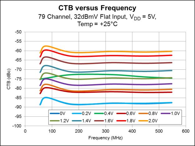
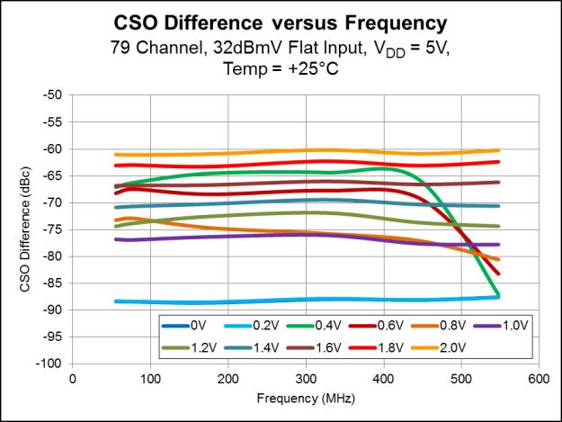
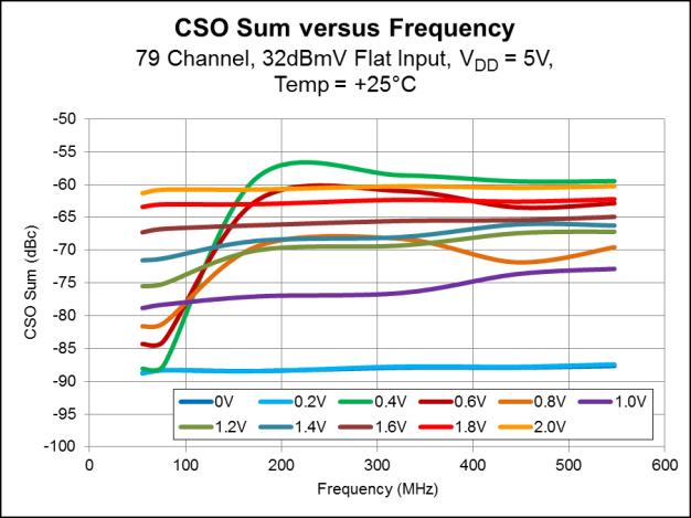
17 Measured CATV Composite Performance: 79 Channel Loading Note: 75Ω Application Circuit 17 of 22


18 Measured CATV Composite Performance: 112 Channel Loading Note: 75Ω Application Circuit 18 of 22
19 CATV Evaluation Board Schematic 75Ω Application Circuit CATV Evaluation Board Bill of Materials (BOM) Note: 75Ω Application Circuit Description Reference Designator Manufacturer Manufacturer's P/N Voltage Controlled Attenuator VCA, 5V U1 RFMD RFSA3033 CONN, F, EDGE MOUNT, 30 MIL J1-J4 Trompeter Electronics, Inc. CBJE130-2 CONN, HDR, ST, 5-PIN, T/H P1 Molex SA Evaluation Board DDI SA (A) CAP, 1000pF, 10%, 25V, X7R, 0402 C1-C3, C6, C8 Murata Electronics GRM155R71H102KA01D CAP, 1µF, 10%, 16V, X7R, 1206 C4 Murata Electronics GRM31MR71E105KC01L DNP C5, C7 N/A N/A 19 of 22
20 CATV Evaluation Board Assembly Drawing Note: 75Ω Application Circuit 20 of 22
21 Pin Name Description 1 GND Ground Pin 2 GND Ground Pin 3 RFIN RF Input. Use External DC Block 4 GND Ground Pin 5 GND Ground Pin 6 GND Ground Pin 7 GND Ground Pin 8 GND Ground Pin 9 GND Ground Pin 10 RFOUT RF Output. Use External DC Block 11 GND Ground Pin 12 EN Supply Current Enable Control. Connect to Logic Low to Enable. Connect to Logic High to Disable 13 NC Floating Pin, No Connect. 14 VC Attenuator Control Voltage 15 VDD Supply Voltage Pin Names and Description 16 SLOPE Attenuation Slope Control. Connect to Logic Low to Enable Negative Attenuation Slope. Connect to Logic High to Enable Positive Attenuation Slope. GND GND Exposed Package Ground Paddle is RF and DC Ground. 21 of 22
22 Package Drawing 0.9mm x 3.0mm x 3.0mm Laminate Module Branding Diagram 22 of 22
RFSA3043TR7. 75Ω Voltage Controlled Attenuator 5MHz to 3000MHz. Features. Applications. Ordering Information RFSA3043
 75Ω Voltage Controlled Attenuator 5MHz to 3000MHz RFMD s RFSA3043 is a fully monolithic analog voltage controlled attenuator (VCA) featuring exceptional linearity over a typical temperature compensated
GND GND GND. Product Description. Ordering Information. Sample bag with 25 pieces 7 Sample reel with 100 pieces. GaAs MESFET Si BiCMOS Si CMOS Si BJT
 Temperature Compensating Attenuator TEMPERATURE COMPENSATING ATTENUATOR Package: QFN, 16-Pin,.9mm x 3mm x 3mm GND VDD GND GND 16 15 14 13 Features Patent Pending Circuit Architecture Broadband 5MHz to
75 VOLTAGE CONTROLLED ATTENUATOR GND RFIN. Product Description. Ordering Information. GaAs MESFET Si BiCMOS Si CMOS Si BJT
 RFS313 75W Voltage Controlled ttenuator RFS313 75 VOLTGE CONTROLLED TTENUTOR Package Style: QFN, 16-Pin,.9mm x 3mm x 3mm MODE VDD VC GND 16 15 14 13 Features Patent Pending Circuit rchitecture roadband
GND RFIN. Product Description. Ordering Information. GaAs MESFET Si BiCMOS Si CMOS
 RFS213 Voltage Controlled ttenuator RFS213 VOLTGE CONTROLLED TTENUTOR Package Style: QFN, 16-Pin,.9mm x 3mm x 3mm MODE VDD VC GND Features Patent Pending Circuit rchitecture roadband 5MHz to 4MHz Frequency
DATA GND VCC GND RF1 GND GND GND. Product Description. Ordering Information. Sample bag with 25 pieces 7 Sample reel with 100 pieces
 Serial Controlled 75W Digital Step Attenuator 5MHz to 2000MHz, 6- Bit, LSB SERIAL CONTROLLED 75 DIGITAL STEP ATTENUATOR 5MHz TO 2000MHz, 6-BIT, Package: MCM, 24-Pin, 4.2mm x 4.2mm Features Frequency Range
RFVA1017 ANALOG CONTROLLED VARIABLE GAIN AMPLIFIER
 Analog Controlled Variable Gain Amplifier RFVA1017 ANALOG CONTROLLED VARIABLE GAIN AMPLIFIER Package: MCM, 7mm x 7mm VCTRL 8 Features 1425MHz to 1550MHz Operation Gain = 27dB Typical Gain Adjustment Range
RFSW6062 Low Insertion High Isolation SP6T Switch 5MHz to 6000MHz
 Low Insertion High Isolation SP6T Switch 5MHz to 6000MHz The RFSW6062 is a low loss, high isolation SP6T switch with performance optimized for use in Cellular BTS applications. Plus it is also ideally
RFVC1800 Wideband MMIC VCO with Buffer Amplifier 8GHz to 12GHz
 Wideband MMIC VCO with Buffer Amplifier 8GHz to 12GHz RFMD s wideband voltage controlled oscillator is a GaAs InGaP HBT MMIC with integrated VCO core and RF output buffer. The part operates from a single
RFDA4005TR13. 6-Bit, Digital Controlled Variable Gain Amplifier 50MHz to 4000MHz
 6-Bit, Digital Controlled Variable Gain Amplifier 50MHz to 4000MHz RFMD s RFDA4005 is a digitally controlled variable gain amplifier featuring high linearity over the entire gain control range with noise
RFPA3805TR13. GaAs HBT 2-Stage Power Amplifier 700MHz to 2700MHz
 GaAs HBT 2-Stage Power Amplifier 700MHz to 2700MHz RFMD s RFPA3805 is a GaAs HBT linear power amplifier specifically designed for Wireless Infrastructure applications. Using a highly reliable GaAs HBT
RFSA3413TR13. 5 MHz to 6000 MHz Digial Step Attenuator. Product Overview. Key Features. Applications. Functional Block Diagram. Ordering Information
 5 MHz to 6000 MHz Digial Step Attenuator Product Overview The RFMD s is a 4-bit digital step attenuator (DSA) that features high linearity over the entire 15dB gain control range with 1.0dB steps. The
Product Description. Ordering Information. Optimum Technology Matching Applied GaAs HBT GaAs MESFET InGaP HBT
 5MHz to 1MHz, Push-Pull, High Linearity InGaP HBT Amplifier Package Style: SOIC-8 Features 5V Single Supply Excellent Linearity Performance at +34dBmV Output Power per Tone Two Amplifiers in Each SOIC-8
RFDA0045 DIGITAL CONTROLLED VARIABLE GAIN AMPLIFIER 10MHZ TO 850MHZ
 Digital Controlled Variable Gain Amplifier RFDA0045 DIGITAL CONTROLLED VARIABLE GAIN AMPLIFIER 10MHZ TO 850MHZ Package: MCM 32-Pin, 5.2mm x 5.2mm 32 31 30 29 28 27 26 25 RFIN1 RFOUT1 ATTIN ACG1 Product
RFDA3016 Digital Controlled Variable Gain Amplifier 3000MHz to 3800MHz, 6-Bit 0.5dB LSB Control
 Digital Controlled Variable Gain Amplifier 3MHz to 38MHz, 6- Bit.dB LSB Control RFDA316 Digital Controlled Variable Gain Amplifier 3MHz to 38MHz, 6-Bit.dB LSB Control Package: MCM 28-Pin, 6.mm x 6.mm 28
RDA1005L DIGITAL CONTROLLED VARIABLE GAIN AMPLIFIER 50 MHZ TO 4000 MHZ, 6 BIT
 Digital Controlled Variable Gain Amplifier 50 MHz to 4000 MHz, 6 Bit RDA1005L DIGITAL CONTROLLED VARIABLE GAIN AMPLIFIER 50 MHZ TO 4000 MHZ, 6 BIT Package: MCM, 32-Pin, 5.2 mm x 5.2 mm Features Broadband
QPC3223TR7. 50 MHz to 6000 MHz Digital Step Attenuator. Product Description. Product Features. Functional Block Diagram.
 5 MHz to 6 MHz Digital Step Attenuator Product Description The is a 2-bit digital step attenuator (DSA) that features high linearity over the entire 18 db gain control range in 6 db steps. The uses a parallel
RFVC GHz to 12.1GHz MMIC VCO with Fo/2 and Fo/4 Outputs
 10.8GHz to 12.1GHz MMIC VCO with Fo/2 and Fo/4 Outputs RFMD's RFVC1844 is a 5V InGaP MMIC VCO with an integrated frequency divider providing additional Fo/2 and Fo/4 outputs. With an Fo frequency range
RFGA0024. InGaP HBT. 1000MHz. Product Description. Ordering Information
 InGaP HBT MMIC Amplifier 5MHz TO 1MHz RFGA24 InGaP HBT MMIC Amplifier 5MHz TO 1MHz Package: SOT-89 Features Low Cost Broadband Gain Internally Matched Internal Active Bias No Dropping Resistor Single Supply
RFVC1843TR7. 9.8GHz to 11.3GHz MMIC VCO with Fo/2 and Fo/4 Outputs. Features. Applications. Ordering Information
 RFVC1843 9.8GHz to 11.3GHz MMIC VCO with Fo/2 and Fo/4 Outputs RFMD's RFVC1843 is a 5V InGaP MMIC VCO with an integrated frequency divider providing additional Fo/2 and Fo/4 outputs. With an Fo frequency
QPC6054SR. Product Description. Product Features. Functional Block Diagram. Applications. Ordering Information
 RFC VSS/ V3 Product Description The is a Silicon on Insulator (SOI) single-pole, 5- throw (SP5T) switch design for use in cellular, 3G, LTE and other high performance communications systems. It offers
Features. = +25 C, 50 Ohm system
 HMC12ALC4 Typical Applications v7.617 ATTENUATOR, 5-3 GHz Features The HMC12ALC4 is ideal for: Point-to-Point Radio VSAT Radio Test Instrumentation Microwave Sensors Military, ECM & Radar Functional Diagram
IDTF2255NLGK8. IDTF2255NLGK Datasheet GENERAL DESCRIPTION FEATURES COMPETITIVE ADVANTAGE DEVICE BLOCK DIAGRAM ORDERING INFORMATION APPLICATIONS
 1MHz to 3MHz GENERAL DESCRIPTION The IDTF2255 is a low insertion loss Voltage Variable RF Attenuator (VVA) designed for a multitude of wireless and other RF applications. This device covers a broad frequency
Preliminary C0.25 VDD N/C RF1 N/C N/C. Product Description. Ordering Information
 RFSA74 Parallel Controlled Digital Step Attenuator 5MHz to 4MHz, 7-Bit,.5dB LSB Package Style: QFN 4-Pin, 4mm x 4 mm Features C.5 C C C4 C8 C6 4 3 9 Frequency Range 5MHz to 4MHz 7-Bit, 3.75dB Range,.5dB
RFDA0056 Digital Controlled Variable Gain Amplifier 300MHz to 1100MHz, 6-Bit 0.5dB LSB Control
 Digital Controlled Variable Gain Amplifier 3MHz to MHz, 6- Bit.dB LSB Control RFDA6 Digital Controlled Variable Gain Amplifier 3MHz to MHz, 6-Bit.dB LSB Control Package: MCM 8-Pin, 6.mm x 6.mm 8 7 6 3
Not For New Design FMS W GaAs phemt SPDT SWITCH. Product Description. Features. Applications
 10W GaAs phemt SPDT Switch FMS2031-001 10W GaAs phemt SPDT SWITCH Package: 3 mm x 3 mm QFN Product Description The FMS2031-001 is a 10 W, Single-pole, Double-throw, (SPDT) GaAs phemt reflective antenna
IDTF2250NLGK8. IDTF2250NLGK Datasheet GENERAL DESCRIPTION FEATURES COMPETITIVE ADVANTAGE DEVICE BLOCK DIAGRAM ORDERING INFORMATION APPLICATIONS
 IDTF225NLGK 5MHz to 6MHz GENERAL DESCRIPTION The IDTF225 is a low insertion loss Voltage Variable RF Attenuator (VVA) designed for a multitude of wireless and other RF applications. This device covers
GND/NC VDD GND/NC RF1 GND/NC GND/NC. Product Description. Ordering Information
 RFS2724Parallel Controlled Digital Step ttenuator, 50MHz to 400MHz RFS2724 Serial Controlled Digital Step ttenuator, 50MHz to 4000MHz Package: MCM, 24-Pin, 4.2mm x 4.2mm DT NC LE CLK PUP NC 24 23 22 21
QPB7400SR QPB7400PCK. CATV 75Ω Adjustable Low Gain (9 11dB) RF Amplifier. Product Overview. Key Features. Functional Block Diagram.
 RF Amplifier. Product Overview. Key Features. Functional Block Diagram.") Product Overview The is a low-cost RF amplifier designed for applications from 47 to 1218 MHz. The balance of low noise and distortion provides an ideal solution for a wide range of broadband amplifiers
Product Overview The is a low-cost RF amplifier designed for applications from 47 to 1218 MHz. The balance of low noise and distortion provides an ideal solution for a wide range of broadband amplifiers
QPB3311SR. 15 db Return Path Amplifier MHz. Product Overview. Key Features. Functional Block Diagram. Applications. Ordering Information
 Product Overview The is an HBT single ended RF amplifier IC operating as return path amplifier capable of supporting DOCSIS 3.1 applications. This IC is designed to provide a low noise, high gain option
Absolute Maximum Ratings Parameter Rating Unit Max Input Power, OFDM Modulated, 3:1 Load VSWR +39 dbm Max Input Power, 2:1 VSWR +41 dbm ESD HBM Rating
 1W GaAs phemt SPDT Switch FMS231-1 1W GaAs phemt SPDT SWITCH Package: 3mmx3mm QFN Product Description The FMS231-1 is a 1W, Single-pole, Double-throw, (SPDT) GaAs phemt reflective antenna switch. The switch
Product Description. GaAs HBT GaAs MESFET InGaP HBT
 Direct Quadrature Modulator RFMD0014 DIRECT QUADRATURE MODULATOR Package: QFN, 24-Pin, 4mm x 4mm Features ACPR Performance: -70 dbc Typ. for 1-Carrier WCDMA Very High Linearity: +26 dbm OIP3 Very Low Noise
10 W, GaN Power Amplifier, 2.7 GHz to 3.8 GHz HMC1114
 9 13 16 FEATURES High saturated output power (PSAT): 41.5 dbm typical High small signal gain: db typical High power gain for saturated output power:.5 db typical Bandwidth: 2.7 GHz to 3.8 GHz High power
Features. = +25 C, Vcc = 5V, Vpd = 5V. Parameter Min. Typ. Max. Min. Typ. Max. Units
 v2.717 MMIC AMPLIFIER, 4 - GHz Typical Applications The is ideal for: Cellular / PCS / 3G Fixed Wireless & WLAN CATV, Cable Modem & DBS Microwave Radio & Test Equipment IF & RF Applications Functional
GaAs, phemt, MMIC, Single Positive Supply, DC to 7.5 GHz, 1 W Power Amplifier HMC637BPM5E
 9 11 13 31 NIC 3 ACG1 29 ACG2 2 NIC 27 NIC 26 NIC GaAs, phemt, MMIC, Single Positive Supply, DC to 7.5 GHz, 1 W Power Amplifier FEATURES P1dB output power: 2 dbm typical Gain:.5 db typical Output IP3:
Analog Devices Welcomes Hittite Microwave Corporation NO CONTENT ON THE ATTACHED DOCUMENT HAS CHANGED
 Analog Devices Welcomes Hittite Microwave Corporation NO CONTENT ON THE ATTACHED DOCUMENT HAS CHANGED www.analog.com www.hittite.com THIS PAGE INTENTIONALLY LEFT BLANK v3.1211 45 Analog Phase Shifter,
Product Description. Ordering Information. GaAs MESFET Si BiCMOS
 Digital Controlled Variable Gain Amplifier 1700MHz to 2400MHz RFDA2077 DIGITAL CONTROLLED VARIABLE GAIN AMPLIFIER 1700MHz to 2400MHz Package: MCM 32-Pin, 7.0mmx7.0mm Features Dual Channel VGA Frequency
10 W, Failsafe, GaAs, SPDT Switch 0.2 GHz to 2.7 GHz HMC546LP2E
 FEATURES High input P.dB: 4 dbm Tx Low insertion loss:.4 db High input IP3: 67 dbm Positive control: V low control; 3 V to 8 V high control Failsafe operation: Tx is on when no dc power is applied APPLICATIONS
Monolithic Amplifier PGA Flat Gain, High Dynamic Range to 1.5 GHz. The Big Deal
 Flat Gain, High Dynamic Range Monolithic Amplifier 75Ω 0.05 to 1.5 GHz The Big Deal High IP3 and IP2 Flat Gain / Excellent Return Loss Low Noise Figure SOT-89 PACKAGE Product Overview (RoHS compliant)
IDTF2258NLGK8. IDTF2258NLGK Datasheet FEATURES GENERAL DESCRIPTION FUNCTIONAL BLOCK DIAGRAM COMPETITIVE ADVANTAGE ORDERING INFORMATION APPLICATIONS
 IDTF2258NLGK Datasheet Voltage Variable RF Attenuator GENERAL DESCRIPTION The F2258 is a low insertion loss Voltage Variable RF Attenuator (VVA) designed for a multitude of wireless and other RF applications.
RFSW1012SR. Broadband SPDT Switch. Product Overview. Key Features. Functional Block Diagram. Ordering Information
 Product Overview The is a single-pole double-throw (SPDT) switch designed for applications requiring very low insertion loss and high power handling capability. The excellent linearity performance of the
F2270 Datasheet VMODE VCTRL VDD. Control RF2 RF1. 75Ω Voltage Variable Attenuator 5MHz to 3000MHz. Features. Description. Competitive Advantage
 75Ω Voltage Variable Attenuator 5MHz to 3000MHz F2270 Datasheet Description The F2270 is a 75Ω, low insertion loss voltage variable RF attenuator (VVA) designed for a multitude of wireless and other RF
Features. Gain: 14.5 db. Electrical Specifications [1] [2] = +25 C, Rbias = 825 Ohms for Vdd = 5V, Rbias = 5.76k Ohms for Vdd = 3V
![Features. Gain: 14.5 db. Electrical Specifications [1] [2] = +25 C, Rbias = 825 Ohms for Vdd = 5V, Rbias = 5.76k Ohms for Vdd = 3V](/thumbs/90/101370216.jpg "Features. Gain: 14.5 db. Electrical Specifications [1] [2] = +25 C, Rbias = 825 Ohms for Vdd = 5V, Rbias = 5.76k Ohms for Vdd = 3V") Typical Applications The HMC77ALP3E is ideal for: Fixed Wireless and LTE/WiMAX/4G BTS & Infrastructure Repeaters and Femtocells Public Safety Radio Access Points Functional Diagram Features Noise Figure:.
Typical Applications The HMC77ALP3E is ideal for: Fixed Wireless and LTE/WiMAX/4G BTS & Infrastructure Repeaters and Femtocells Public Safety Radio Access Points Functional Diagram Features Noise Figure:.
HMC540SLP3E v db LSB SILICON MMIC 4-BIT DIGITAL POSITIVE CONTROL ATTENUATOR, GHz
 HMC54SLP3E v.95 LSB SILICON MMIC 4-BIT DIGITAL POSITIVE CONTROL ATTENUATOR,. - 8 GHz Typical Applications Features The HMC54SLP3E is ideal for both RF and IF applications: Cellular Infrastructure Wireless
CGA-6618Z Dual CATV 5MHz to 1000MHz High Linearity GaAs HBT Amplifier CGA-6618Z DUAL CATV 5MHz to 1000MHz HIGH LINEARITY GaAs HBT AMPLIFIER Package: E
 Dual CATV 5MHz to 1MHz High Linearity GaAs HBT Amplifier DUAL CATV 5MHz to 1MHz HIGH LINEARITY GaAs HBT AMPLIFIER Package: ESOP- Product Description RFMD s CGA-1Z is a high performance GaAs HBT MMIC amplifier.
Features. = +25 C, IF = 100 MHz, LO = +13 dbm, LSB [1]
![Features. = +25 C, IF = 100 MHz, LO = +13 dbm, LSB [1]](/thumbs/85/92081906.jpg "Features. = +25 C, IF = 100 MHz, LO = +13 dbm, LSB [1]") v1.6 3.5 - GHz Typical Applications The HMC21BMSGE is ideal for: Base stations, Repeaters & Access Points WiMAX, WiBro & Fixed Wireless Portables & Subscribers PLMR, Public Safety & Telematics Functional
v1.6 3.5 - GHz Typical Applications The HMC21BMSGE is ideal for: Base stations, Repeaters & Access Points WiMAX, WiBro & Fixed Wireless Portables & Subscribers PLMR, Public Safety & Telematics Functional
Features. = +25 C, Vdd = +10 V, Idd = 350 ma
 HMC97APME v2.4 POWER AMPLIFIER,.2-22 GHz Typical Applications The HMC97APME is ideal for: Test Instrumentation Military & Space Functional Diagram Features High P1dB Output Power: + dbm High : 14 db High
RFIN 2 GND. Product Description. Ordering Information. GaAs HBT GaAs MESFET. InGaP HBT
 InGaP HBT Low Power Linear Amplifier RFGA212 InGaP HBT LOW POWER LINEAR AMPLIFIER Package: DFN, -Pin, 2mmx2mm Features High OIP3=35dBm at 196MHz 1 VBIAS Low DC Power: 3.3V, 23mA Low NF = 1.6dB at 196MHz
4 GHz to 18 GHz Divide-by-4 Prescaler ADF5001
 4 GHz to 18 GHz Divide-by-4 Prescaler ADF5001 FEATURES Divide-by-4 prescaler High frequency operation: 4 GHz to 18 GHz Integrated RF decoupling capacitors Low power consumption Active mode: 30 ma Power-down
20 MHz to 500 MHz IF Gain Block ADL5531
 20 MHz to 500 MHz IF Gain Block ADL5531 FEATURES Fixed gain of 20 db Operation up to 500 MHz Input/output internally matched to 50 Ω Integrated bias control circuit Output IP3 41 dbm at 70 MHz 39 dbm at
OBSOLETE. = +25 C, Vdd = Vs= +5V, Vctl= 0/ +5V. Parameter Frequency Min. Typ. Max. Units DC GHz 37. db Gain (Maximum Gain State)
") v.1212.5 db LSB GaAs MMIC 6-BIT DIGITAL Typical Applications The is ideal for: IF & RF Applications Cellular/3G Infrastructure WiBro / WiMAX / 4G Microwave Radio & VSAT Test Equipment and Sensors Functional
v.1212.5 db LSB GaAs MMIC 6-BIT DIGITAL Typical Applications The is ideal for: IF & RF Applications Cellular/3G Infrastructure WiBro / WiMAX / 4G Microwave Radio & VSAT Test Equipment and Sensors Functional
F2976 Datasheet. High Linearity Broadband SP2T 5MHz to 10GHz. Features (50Ω) Description. Competitive Advantage. Typical Applications.
 Description. Competitive Advantage. Typical Applications.") High Linearity Broadband SP2T 5MHz to 1GHz F2976 Datasheet Description The F2976 is a single-pole double-throw (SP2T) reflective RF switch featuring high linearity and wide bandwidth. This device is optimized
High Linearity Broadband SP2T 5MHz to 1GHz F2976 Datasheet Description The F2976 is a single-pole double-throw (SP2T) reflective RF switch featuring high linearity and wide bandwidth. This device is optimized
= +25 C, With Vee = -5V & Vctl = 0/-5V
 v.46.5db LSB GaAs MMIC 6-BIT DIGITAL Typical Applications Features The HMC44AG6 is ideal for: Telecom Infrastructure Military Radios, Radar & ECM Space Applications Test Instrumentation Functional Diagram.5
Features OBSOLETE. = +25 C, 50 Ohm System GHz degrees Insertion Loss 6-15 GHz 8 11 db. Return Loss (Input and Output) 6-15 GHz 7 db
 6-15 GHz 7 db") v2.29 6 ANALOG PHASE SHIFTER, 1 Typical Applications The HMC538LP4 / HMC538LP4E is ideal for: Fiber Optics Military Test Equipment Functional Diagram Features Electrical Specifications, T A = +25 C, 5
v2.29 6 ANALOG PHASE SHIFTER, 1 Typical Applications The HMC538LP4 / HMC538LP4E is ideal for: Fiber Optics Military Test Equipment Functional Diagram Features Electrical Specifications, T A = +25 C, 5
Features. = +25 C, 50 Ohm system
 v6.312 Typical Applications Features The E is ideal for: Point-to-Point Radio VSAT Radio Test Instrumentation Microwave Sensors Military, ECM & Radar Functional Diagram Wide Bandwidth: 5-26.5 GHz Excellent
RF5632 SINGLE 5.0V, 2.3 TO 2.7 GHZ LINEAR POWER AMPLIFIER
 Single 5.0V, 2.3 to 2.7 GHz Linear Power Amplifier RF5632 SINGLE 5.0V, 2.3 TO 2.7 GHZ LINEAR POWER AMPLIFIER Package Style: QFN, 24-Pin, 4mmx4mmx0.9mm VBIAS VC1 24 23 22 21 20 VC2 19 Features 34dB Small
Features = +5V. = +25 C, Vdd 1. = Vdd 2
 v7.11 HMC1LC3 POWER AMPLIFIER, - GHz Typical Applications The HMC1LC3 is ideal for use as a medium power amplifier for: Microwave Radio & VSAT Military & Space Test Equipment & Sensors Fiber Optics LO
4 GHz to 18 GHz Divide-by-8 Prescaler ADF5002
 4 GHz to 18 GHz Divide-by-8 Prescaler ADF5002 FEATURES Divide-by-8 prescaler High frequency operation: 4 GHz to 18 GHz Integrated RF decoupling capacitors Low power consumption Active mode: 30 ma Power-down
Nonreflective, Silicon SP4T Switch, 0.1 GHz to 6.0 GHz HMC7992
 Nonreflective, Silicon SP4T Switch,.1 GHz to 6. GHz FEATURES Nonreflective, 5 Ω design High isolation: 45 db typical at 2 GHz Low insertion loss:.6 db at 2 GHz High power handling 33 dbm through path 27
Parameter Frequency Min. Typ. Max. Units GHz GHz Attenuation Range GHz 31.5 db
 v.37. db LSB GaAs MMIC 6-BIT DIGITAL POSITIVE CONTROL ATTENUATOR,. - 8. GHz Typical Applications Features ATTENUATORS - SMT The HMCALP3E is ideal for: WLAN & Point-to-Multi-Point Fiber Optics & Broadband
Features. = +25 C, Vdd= 8V, Vgg2= 3V, Idd= 290 ma [1]
![Features. = +25 C, Vdd= 8V, Vgg2= 3V, Idd= 290 ma [1]](/thumbs/95/123095816.jpg "Features. = +25 C, Vdd= 8V, Vgg2= 3V, Idd= 290 ma [1]") Typical Applications The is ideal for: Telecom Infrastructure Microwave Radio & VSAT Military EW, ECM & C 3 I Test Instrumentation Fiber Optics Functional Diagram Features P1dB Output Power: + dbm Gain:
Typical Applications The is ideal for: Telecom Infrastructure Microwave Radio & VSAT Military EW, ECM & C 3 I Test Instrumentation Fiber Optics Functional Diagram Features P1dB Output Power: + dbm Gain:
High Isolation, Silicon SP4T, Nonreflective Switch, 9 khz to 12.0 GHz ADRF5040
 RF4 RF3 7 8 9 1 11 12 21 2 19 RF2 High Isolation, Silicon SP4T, Nonreflective Switch, 9 khz to 12. GHz ADRF54 FEATURES FUNCTIONAL BLOCK DIAGRAM Nonreflective 5 Ω design Positive control range: V to 3.3
RFPD2650 GaAs/GaN Power Doubler Hybrid 45MHz to 1003MHz
 GaAs/GaN Power Doubler Hybrid 45MHz to 1003MHz The RFPD2650 is a Hybrid Power Doubler amplifier module. The part employs GaAs phemt die and GaN HEMT die, has extremely high output capability, and is operated
HMC629ALP4E. 3 db LSB GaAs MMIC 4-BIT DIGITAL ATTENUATOR, DC - 10GHz. Typical Applications. Functional Diagram. General Description
 v1.716 DIGITAL ATTENUATOR, DC - 1GHz Typical Applications The is ideal for: Cellular/3G Infrastructure WiBro / WiMAX / 4G Microwave Radio & VSAT Test Equipment and Sensors IF & RF Applications Functional
Parameter Frequency (GHz) Min. Typ. Max. Units DC GHz GHz GHz Attenuation Range DC GHz 31.5 db
 Min. Typ. Max. Units DC GHz GHz GHz Attenuation Range DC GHz 31.5 db") Typical Applications The is ideal for: 3G Infrastructure & access points Cellular/3G, LTE & UMB WiMAX, WiBN & Fixed Wireless Test Equipment and Sensors GSM, WCDMA & TD-SCDMA Functional Diagram Features.5
Typical Applications The is ideal for: 3G Infrastructure & access points Cellular/3G, LTE & UMB WiMAX, WiBN & Fixed Wireless Test Equipment and Sensors GSM, WCDMA & TD-SCDMA Functional Diagram Features.5
Features. = +25 C, Vdd = +15V, Vgg2 = +9.5V [1], Idq = 500 ma [2]
![Features. = +25 C, Vdd = +15V, Vgg2 = +9.5V [1], Idq = 500 ma [2]](/thumbs/88/115381636.jpg "Features. = +25 C, Vdd = +15V, Vgg2 = +9.5V [1], Idq = 500 ma [2]") v3.41 Typical Applications Features The is ideal for: Test Instrumentation Military & Space Fiber optics Functional Diagram P1dB Output Power: + dbm Psat Output Power: + dbm High Gain: db Output IP3: 42
v3.41 Typical Applications Features The is ideal for: Test Instrumentation Military & Space Fiber optics Functional Diagram P1dB Output Power: + dbm Psat Output Power: + dbm High Gain: db Output IP3: 42
HMC629ALP4E. 3 db LSB GaAs MMIC 4-BIT DIGITAL ATTENUATOR, DC - 10GHz. Typical Applications. Functional Diagram. General Description
 Typical Applications The is ideal for: Cellular/3G Infrastructure WiBro / WiMAX / 4G Microwave Radio & VSAT Test Equipment and Sensors IF & RF Applications Functional Diagram Features 3 LSB Steps to 45
RF2420. Typical Applications Power Control in Communication Systems CMOS Compatible Programmable Attenuators
 RF2420 PROGRAMMABLE ATTENUATOR Typical Applications Power Control in Communication Systems CMOS Compatible Programmable Attenuators Commercial and Consumer Systems Portable Battery-Powered Equipment Product
QPB2318SR. 15 db Balanced Return Path Amplifier MHz. Product Overview. Functional Block Diagram. Ordering Information
 Product Overview The is an HBT RF balanced amplifier IC operating as a return path amplifier capable of supporting DOCSIS 3.1 applications. This IC is designed to provide a low noise, high gain option
RF OUT / N/C RF IN / V G
 MAAM-111 MHz - 2 GHz Rev. V2 Features Functional Schematic 12 db Gain Ω Input / Output Match over Gain Range 3 db Gain Control with to -2 V Control +18 dbm Output Power + V, -. V DC, 7 ma Lead-Free 1.
2 GHz to 28 GHz, GaAs phemt MMIC Low Noise Amplifier HMC7950
 Data Sheet FEATURES Output power for db compression (PdB): 6 dbm typical Saturated output power (PSAT): 9. dbm typical Gain: db typical Noise figure:. db typical Output third-order intercept (IP3): 6 dbm
5.5 GHz to 8.6 GHz, GaAs, MMIC, I/Q Upconverter HMC6505A
 Data Sheet FEATURES Conversion gain: db typical Sideband rejection: dbc typical Output P1dB compression at maximum gain: dbm typical Output IP3 at maximum gain: dbm typical LO to RF isolation: db typical
Amplifier Configuration
 Dual CATV Broadband High Linearity SiGe HBT Amplifier CGA-33Z DUAL CATV BROADBAND HIGH LINEARITY SiGe HBT AMPLIFIER Package: ESOP- Product Description RFMD s CGA-33Z is a high performance Silicon Germanium
OBSOLETE HMC5846LS6 AMPLIFIERS - LINEAR & POWER - SMT. Electrical Specifications, T A. Features. Typical Applications. General Description
 v1.414 Typical Applications The HMC846LS6 is ideal for: Point-to-Point Radios Point-to-Multi-Point Radios VSAT & SATCOM Military & Space Functional Diagram Electrical Specifications, T A = +2 C Vdd = Vdd1,
Product Description. Ordering Information. GaAs HBT GaAs MESFET InGaP HBT
 RFPA38 GaAs HBT 15MHz TO 96MHz POWER AMPLIFIER Package: SOIC-8 Features 5W Output Power (P1dB) High Linearity: OIP3>48dBm High Efficiency Low Noise: NF=3.2dB at 945MHz 5V to 7V Operation Thermally Enhanced
Features. = +25 C, Vcc1 = Vcc2 = 5V, Zo = 75 Ohm [1]
![Features. = +25 C, Vcc1 = Vcc2 = 5V, Zo = 75 Ohm [1]](/thumbs/87/97046026.jpg "Features. = +25 C, Vcc1 = Vcc2 = 5V, Zo = 75 Ohm [1]") HMC754SGE v.49 Typical Applications The HMC754SGE is ideal for: CATV / Broadband Infrastructure Test & Measurement Equipment Line Amps and Fiber Nodes Customer Premise Equipment Functional Diagram Output
HMC754SGE v.49 Typical Applications The HMC754SGE is ideal for: CATV / Broadband Infrastructure Test & Measurement Equipment Line Amps and Fiber Nodes Customer Premise Equipment Functional Diagram Output
Features OBSOLETE. = +25 C, Rbias = 0 Ohm. Bypass Mode Failsafe Mode Parameter
 7 Typical Applications The HMC668LP3(E) is ideal for: Cellular/3G and LTE/WiMAX/4G BTS & Infrastructure Repeaters and Femtocells Tower Mounted Amplifiers Test & Measurement Equipment Functional Diagram
Features. Output Power for 1 db Compression (P1dB) dbm Saturated Output Power (Psat) dbm
 dbm Saturated Output Power (Psat) dbm") v1.314 Typical Applications Features The is ideal for: Test Instrumentation Microwave Radio & VSAT Telecom Infrastructure Military & Space Fiber optics Functional Diagram P1dB Output Power: +27 dbm Psat
v1.314 Typical Applications Features The is ideal for: Test Instrumentation Microwave Radio & VSAT Telecom Infrastructure Military & Space Fiber optics Functional Diagram P1dB Output Power: +27 dbm Psat
Broadband covering primary wireless communications bands: Cellular, PCS, LTE, WiMAX
 Ultra Linear Low Noise Monolithic Amplifier 50Ω 0.05 to 4 GHz The Big Deal Ultra High IP3 Broadband High Dynamic Range May be used as a replacement for RFMD SPF-5189Z a,b SOT-89 PACKAGE Product Overview
ACA2417: 1218 MHz CATV Push-Pull Driver Amplifier
 DATA SHEET ACA2417: 1218 MHz CATV Push-Pull Driver Amplifier Applications DOCSIS and Euro DOCSIS 3.1 (D3.1) compliant downstream RF Pre-amplifier for node + 0 HFC and FTTC/FTTB networks Final stage amplifier
Data Sheet. ALM MHz 4GHz PIN Diode Variable Attenuator Module. Description. Features. Specifications. Applications.
 ALM-38140 50MHz 4GHz PIN Diode Variable Attenuator Module Data Sheet Description Avago Technologies ALM-38140 is a fully matched wideband variable attenuator module with high linearity performance and
20 MHz to 500 MHz IF Gain Block ADL5531
 Data Sheet FEATURES Fixed gain of 20 db Operation up to 500 MHz Input/output internally matched to 50 Ω Integrated bias control circuit Output IP3 41 dbm at 70 MHz 39 dbm at 190 MHz Output 1 db compression:
HMC6380LC4B. WIDEBAND VCOs - SMT. Electrical Specifications, T A. Typical Applications. Features. General Description. Functional Diagram
 Typical Applications Low Noise wideband MMIC VCO is ideal for: Industrial/Medical Equipment Test & Measurement Equipment Satcom Military Radar, EW, & ECM Functional Diagram Features Wide Tuning Bandwidth
Monolithic Amplifier PHA-202+ Ultra High Dynamic Range to 2.7 GHz. The Big Deal
 Ultra High Dynamic Range Monolithic Amplifier 50Ω 0.03 to 2.7 GHz The Big Deal Ultra High IP3, +46.1 dbm Broadband High Dynamic Range without external Matching Components Medium power, 1W Excellent return
Analog Devices Welcomes Hittite Microwave Corporation NO CONTENT ON THE ATTACHED DOCUMENT HAS CHANGED
 Analog Devices Welcomes Hittite Microwave Corporation NO CONTENT ON THE ATTACHED DOCUMENT HAS CHANGED www.analog.com www.hittite.com THIS PAGE INTENTIONALLY LEFT BLANK v1.414 Typical Applications The HMC5846LS6
OBSOLETE. Active RF Splitter ADA FEATURES FUNCTIONAL BLOCK DIAGRAM APPLICATIONS GENERAL DESCRIPTION
 FEATURES Single V supply 4 MHz to 86 MHz CATV operating range 4.6 db of gain per output channel 4.4 db noise figure 2 db isolation between output channels 16 db input return loss CSO of 73 dbc (13 channels,
= +25 C, with Vcc = +5V. Parameter Frequency (GHz) Min. Typ. Max. Units DC GHz GHz GHz Attenuation Range DC GHz 31.
 Min. Typ. Max. Units DC GHz GHz GHz Attenuation Range DC GHz 31.") Typical Applications The is ideal for: Cellular/PCS/3G Infrastructure ISM, MMDS, WLAN, WiMAX, & WiBro Microwave Radio & VSAT Test Equipment and Sensors Functional Diagram Features.5 db LSB Steps to 31.5
Typical Applications The is ideal for: Cellular/PCS/3G Infrastructure ISM, MMDS, WLAN, WiMAX, & WiBro Microwave Radio & VSAT Test Equipment and Sensors Functional Diagram Features.5 db LSB Steps to 31.5
High Isolation, Silicon SPDT, Nonreflective Switch, 0.1 GHz to 6.0 GHz HMC8038W
 5 6 7 8 6 5 4 3 FEATURES Nonreflective, 50 Ω design High isolation: 60 db typical Low insertion loss: 0.8 db typical High power handling 34 dbm through path 29 dbm terminated path High linearity P0.dB:
SZM-3066Z. 3.3GHz to 3.8GHz 2W POWER AMPLIFIER. Product Description. Features. Applications. Package: QFN, 6mmx6mm
 3.3GHz to 3.8GHz 2W Power Amplifier SZM-3066Z 3.3GHz to 3.8GHz 2W POWER AMPLIFIER Package: QFN, 6mmx6mm Product Description RFMD s SZM-3066Z is a high linearity class AB Heterojunction Bipolar Transistor
Broadband covering primary wireless communications bands: Cellular, PCS, LTE, WiMAX
 High Gain, High IP3 Monolithic Amplifier 50Ω 0.01 to 6 GHz The Big Deal High Gain Broadband High Dynamic Range without external Matching Components May be used as a replacement to RFMD SBB5089Z a,b SOT-89
40MHz to 4GHz Linear Broadband Amplifiers
 MAX26 MAX26 0MHz to GHz Linear Broadband Amplifiers General Description The MAX26 MAX26 is a family of high-performance broadband gain blocks designed for use as a PA predriver, low-noise amplifier, or
Features. Gain: 17 db. OIP3: 25 dbm. = +25 C, Vdd 1, 2 = +3V
 v.7 HMCLC Typical Applications The HMCLC is ideal for use as a LNA or driver amplifier for: Point-to-Point Radios Point-to-Multi-Point Radios & VSAT Test Equipment and Sensors Military & Space Functional
RFHA1004TR7. 25W GaN Wide-Band Power Amplifier 700MHz to 2500MHz. Features. Applications. Ordering Information. Package: Air-Cavity Cu
 25W GaN Wide-Band Power Amplifier 700MHz to 2500MHz The is a wideband Power Amplifier designed for CW and pulsed applications such as wireless infrastructure, RADAR, military communication radios and general
F2972 Datasheet. High Linearity Broadband SP2T 5MHz to 10GHz. Description. Features (50Ω) Competitive Advantage. Typical Applications.
 Competitive Advantage. Typical Applications.") High Linearity Broadband SP2T 5MHz to 1GHz F2972 Datasheet Description The F2972 is a single-pole double-throw (SP2T) reflective RF switch featuring high linearity and wide bandwidth. This device is optimized
High Linearity Broadband SP2T 5MHz to 1GHz F2972 Datasheet Description The F2972 is a single-pole double-throw (SP2T) reflective RF switch featuring high linearity and wide bandwidth. This device is optimized
RF2317. Laser Diode Driver Return Channel Amplifier Base Stations. CATV Distribution Amplifiers Cable Modems Broadband Gain Blocks
 CATV Distribution Amplifiers Cable Modems Broadband Gain Blocks Laser Diode Driver Return Channel Amplifier Base Stations The is a general purpose, low cost high linearity RF amplifier IC. The device is
QPC7336TR13. 45MHz to 1218MHz Variable Equalizer. Product Description. Product Features. Functional Block Diagram. Applications. Ordering Information
 45MHz to 1218MHz Variable Equalizer Product Description The QPC7336 is a voltage controlled variable equalizer employing SOI attenuator, optimized for DOCSIS 3.1 operation between 45MHz and 1218MHz. 14
HMC849ALP4CE SWITCHES - SPDT - SMT. HIGH ISOLATION SPDT NON-REFLECTIVE SWITCH, DC - 6 GHz. Typical Applications. Features. Functional Diagram
 Typical Applications The is ideal for: Cellular/4G Infrastructure WiMAX, WiBro & Fixed Wireless Automotive Telematics Mobile Radio Test Equipment Functional Diagram Features High Isolation: up to Single
Features. = +25 C, 50 Ohm system. DC - 10GHz DC - 14 Ghz DC - 10 GHz DC - 14 GHz Return Loss DC - 14 GHz 5 10 db
 Typical Applications v2.717 Features The is ideal for: Basestation Infrastructure Fiber Optics & Broadband Telecom Microwave Radio & VSAT Military Radios, Radar, & ECM Test Instrumentation Functional Diagram
= +25 C, With Vee = -5V & VCTL= 0/-5V
 v.3.5db LSB GaAs MMIC 6-BIT DIGITAL Typical Applications Features The is ideal for: Basestation Infrastructure Fiber Optics & Broadband Telecom Microwave & VSAT Radios Military & Space Test Instrumentation
>10 W, GaN Power Amplifier, 0.01 GHz to 1.1 GHz HMC1099
 9 1 11 12 13 14 1 16 32 GND 31 29 28 27 26 FEATURES High saturated output power (PSAT):. dbm typical High small signal gain: 18. db typical High power added efficiency (PAE): 69% typical Instantaneous
50 MHz to 4.0 GHz RF/IF Gain Block ADL5602
 Data Sheet FEATURES Fixed gain of 20 db Operation from 50 MHz to 4.0 GHz Highest dynamic range gain block Input/output internally matched to 50 Ω Integrated bias control circuit OIP3 of 42.0 dbm at 2.0