Outcomes. Spiral 1 / Unit 8. DeMorgan s Theorem DEMORGAN'S THEOREM. Transistor Implementations CMOS Logic Gates
|
|
|
- Julia Flynn
- 6 years ago
- Views:
Transcription
1 Spiral 1 / Unit 8 Transistor Implementations MOS Logic Gates Mark Redekopp Outcomes I know the difference between combinational and sequential logic and can name examples of each. I understand latency, throughput, and at least 1 technique to improve throughput I can identify when I need state vs. a purely combinational function I can convert a simple word problem to a logic function (TT or canonical form) or state diagram I can use Karnaugh maps to synthesize combinational functions with several outputs I understand how a register with an enable functions & is built I can design a working state machine given a state diagram I can implement small logic functions with complex MOS gates 18.3 emorgan s Theorem 18.4 EMORGN'S THEOREM F = (XY) Z (YW) To find F, invert both sides of the equation and then use emorgan s theorem to simplify F = (XY) Z (YW)

) N s & OR s swapped Each literal is inverted 18.7 18.")
2 Generalized emorgan s Theorem F (X 1,,X n,, ) = F(X 1,,X n,,) To find F, swap N s and OR s and complement each literal. However, you must maintain the original order of operations. emorgan s Theorem Example ancel as many bubbles as you can using emorgan s theorem. Note: This parentheses doesn t matter (we are just OR ing X, Y, and the following subexpression) F = (XY) Z (YW) F = XY (Z (YW)) Fully parenthesized to show original order of ops. F = X Y (Z (Y W)) N s & OR s swapped Each literal is inverted Evolution of transistor in Is With focus on MOS Transistors SEMIONUTOR TEHNOLOGY JT invention, ell Labs, 1947 Single transistor, TI, 1958 MOS gate, Fairchild, 1963 First processor, Intel, 1970 Very Large Scale Integration, 1978 Up to 20k transistor Ultra Large Scale Integration, 1989 More than 1 million per chip System on hip, Millions to several billion transistors


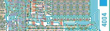
3 Invention of the Transistor Vacuum tubes ruled in first half of 20 th century Large, expensive, power hungry, unreliable 1947: first point contact transistor John ardeen and Walter rattain at ell Labs See rystal Fire by Riordan, Hoddeson Growth Rate 53% compound annual growth rate over 50 years No other technology has grown so fast so long riven by miniaturization of transistors Smaller is cheaper, faster, lower in power! Revolutionary effects on society [Moore65] Electronics Magazine Minimum Feature Size Intel 4004 Micro Processor transistors 1 MHz operation


4 Intel ore I RM ortex nd Gen. Intel ore i7 Extreme Processor for desktops launched in Q4 of 2012 #cores/#threads: 6/12 Technology node: 32nm lock speed: 3.5 GHz Transistor count: Over one billion ache: 15M ddressable memory: 64G Size: 52.5mm by 45.0mm mm 2 RM ortex 15 in 2011 to cores per cluster, two clusters per chip Technology node: 22nm lock speed: 2.5 GHz Transistor count: Over one billion ache: Up to 4M per cluster ddressable memory: up to 1T Size: 52.5mm by 45.0mm 14 ortex IM z13 Storage ontroller 18.16
 0.01 0.001 0.0001 0.00001 0.000001 0.")
5 nnual Sales ost per Transistor >10 19 transistors manufactured in billion for every human on the planet cost: pertransistor Fabrication capital cost per transistor (Moore s law) Internet Traffic Growth TRNSISTOR SIS
 ominates the digital I market today ll transistors essentially function similarly with 3 nodes/terminals: 1 node serves as the value")
 urrent can flow based on voltage of input switch 18.23 18.")
6 Transistors s Switches Transistor act as a form of switch (on / off) ifferent physical structures lead to different kinds of transistors ipolar Junction Transistor (JT) Initial technology back in the late 40's 60's Metal Oxide Semiconductor Transistor (MOSFET) ominates the digital I market today ll transistors essentially function similarly with 3 nodes/terminals: 1 node serves as the value allowing current to flow between the other 2 nodes (on) or preventing current flow between the other 2 nodes (off) Example: if the switch input voltage is 5V, then current is allowed to flow between the other nodes Semiconductors Switch Input (Hi or Lo Voltage) urrent can flow based on voltage of input switch Semiconductor Material Semiconductor material is not a great conductor material in its pure form Small amount of free charge an be implanted ( ) with other elements (e.g. boron or arsenic) to be more conductive Increases the amount of charge Pure Silicon Type Silicon (oped with boron) Electron acceptors Type Silicon (oped with arsenic) Electron donors
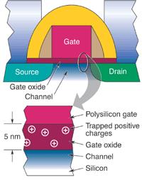
7 Silicon Lattice and opant toms Pure silicon: 3 lattice of atoms (a cubic crystal) and a poor conductor onductivity can be raised by adding either donors or acceptor : Group V dopant impurities, which have more free electrons than silicon The resulting material is called n type Group III dopants impurities which have lack of electrons The resulting material is called p type Transistor Types ipolar Junction Transistors (JT) or silicon structure Small into very thin base layer controls large currents between emitter and collector However the fact that it requires a current into the base means it burns power ( ) and thus how many we can integrate on a chip (i.e. density) Metal Oxide Semiconductor Field Effect Transistors nmos and pmos MOSFETS Voltage applied to insulated gate controls current between source and drain Gate input requires no current thus low power! We will focus on MOSFET in this class emitter ptype ntype ptype base conductive polysilicon ptype Gate Input collector npn JT Ntype MOSFET ntype NMOS Transistor Physics NMOS Transistor Physics Transistor is started by implanting two n type silicon areas, separated by p type thin, insulator layer (silicon dioxide or just oxide ) is placed over the silicon between source and drain ntype silicon (extra negative charges) Source Input rain Output Source Input W L rain Input Insulator Layer (oxide) ntype silicon (extra negative charges) ptype silicon ( extra positive charges) ptype silicon ( extra positive charges)
8 NMOS Transistor Physics NMOS Transistor Physics thin, insulator layer (silicon dioxide or just oxide ) is placed over the silicon between source and drain onductive polysilicon material is layered over the oxide to form the gate input Insulator Layer (oxide) Source Input Gate Input conductive polysilicon ptype silicon ( extra positive charges) rain Output ntype silicon (extra negative charges) voltage (charge) at the gate input repels the extra positive charges in the p type silicon Result is a negativecharge channel between the source input and drain Source Input negativelycharge channel Gate Input positive charge repelled ptype rain Output ntype NMOS Transistor Physics NMOS Transistor Physics Electrons can flow through the negative channel from the source input to the drain output The transistor is Gate Input Source Input rain Output ntype ptype If a voltage (negative charge) is placed on the gate, no channel will develop and no current will flow The transistor is Gate Input Source Input rain Output ntype ptype Negative channel between source and drain = urrent flow No negative channel between source and drain = No current flow
9 PMOS vs. NMOS PMOS transistors can also be made that are on when the gate voltage is and off when it is Source Input Gate Input Negative channel between source and drain = urrent flow ptype rain Output ntype Source Input Gate Input "Positive" channel between source and drain = urrent flow ntype ptype Understanding physical constraints MOS TRNSISTOR LEVEL IMPLEMENTTION NMOS PMOS NMOS and PMOS Transistors NMOS conducts when gate input is at a high voltage (logic 1 ) PMOS conducts when gate input is at a low voltage (logic 0 ) NMOS Transistors 1 0 urrent Flows (Small resistance between source and output ) NMOS (On if G=1) PMOS Transistors No urrent Flows (Large resistance between source and output ) NMOS Transistors in Series/Parallel onnection Transistors can be thought as a switch controlled by its gate signal NMOS switch closes when switch control input is high 1 F F = 1 if Indicates a Ptype urrent Flows (Small resistance between source and output) No urrent Flows (Large resistance between source and output) PMOS (On if G=0) 1 F F = 1 if
10 PMOS Transistors in Series/Parallel onnection We ll Have Our Strengths PMOS switch closes when switch control input is low 1 F 1 F F = 1 if F = 1 if NMOS are: Good at pulling the output voltage ad at pulling the output voltage PMOS are: NMOS Good at pulling the output voltage ad at pulling the output voltage GN Source Gate rain Vdd rain Gate Source Gate Gate PMOS Vdd Source rain GN rain Source NMOS and PMOS Transistors MOS NMOS transistors work best when one terminal is connected to a low voltage source, pulling the other terminal down to that voltage Normally, source terminal is connected to PMOS transistors work best when one terminal is connected to a high voltage source, pulling the other terminal down to that voltage Normally, source terminal is connected to supply voltage (5V, 3V, etc.) NMOS 0V PMOS 3V omplimentary MOS (MOS) Use PMOS to connect output to high voltage source We call this the Pull Up Network Use NMOS to connect output to low voltage source (usually = GN) We call this the Pull own Network Either PMOS or NMOS should create a conductive path to output, but not both Pulldown OFF Pulldown ON Pullup OFF Pullup ON Inputs PullUp Network Pullown Network PMOS Output NMOS
11 Strength of signal Signal Strength How close it approximates ideal voltage source V and GN rails are strongest 1 and 0 nmos passes ut degraded or pmos passes ut degraded or Thus nmoses are best for the pull down network, pmoses are best for the pull up network MOS Inverter Inverter can be formed using one PMOS and NMOS transistor The input value connects to both gate inputs The output is formed at the junction of the drains MOS Inverter MOS NN Gate When input is 1, NMOS conducts and output is pulled down to 0V (GN) When input is 0, PMOS conducts and output is pulled up to 3V (V ) If and = 1, the output of the first circuit is pulled to 0 (opposite of N function) If or = 0, the output of the first circuit is pulled to 1 (opposite of N function) Rule of onduction omplements Pull up network is the dual (complement) of pull down Parallel > series, series > parallel NN
12 MOS N Gate MOS NOR Gate If and = 1, the output of the first circuit is pulled to 0 (opposite of N function) If or = 0, the output of the first circuit is pulled to 1 (opposite of N function) Inverter is then used to produce true N output If or = 1, the output of the first circuit is pulled to 0 (opposite of OR function) If and = 0, the output of the circuit is pulled to 1 (opposite of OR function) Rule of onduction omplements Pull up network is the dual (complement) of pull down Parallel > series, series > parallel NOR NN Inverter to produce N MOS NOR Gate ompound Gates If or = 1, the output of the first circuit is pulled to 0 (opposite of OR function) If and = 0, the output of the circuit is pulled to 1 (opposite of OR function) Inverter is then used to produce true OR output OR How could you build this gate? You could try building each gate separately Two N gates = transistors One NOR gate = transistors With emorgan's Two NN gates = transistors One N gate = transistors Or you could take build it as a single compound gate. F F
13 ompound Gates ompound gates can do any inverting function Ex: N OR INVERT (OI) Full Gate Separate (a) Y = Separate Separate '' Separate (c) '' Y (b) (d) (f) ('')('') Y PN PUN ompound Gate pproach For an inverting function just look at the expression (w/o the inversion) and Implement the PN using: Series connections for Parallel connections for Implement PUN as dual of PN Swap and If function is non inverting just add an inverter at the (e) ompound Gate Example ompound Gate Example Y = ( ) OUT = ( )
14 ompound Gate Example (cont.) nother ompound Gate Example This is really a MOS inverter (2 transistors) but we just show it this way to save space and focus on the 1 st stage cell OUT = ( E) OUT = ( E) dd an inverter at the output Implement inverting function using compound MOS gate OR apply emorgan's theorem with the inner inversion and just build the resulting circuit OUT = uild a 2 to 1 mux at the Transistor Level I 0 Y? I 1 S FRITION
 and p channel (PMOS) transistors are built on the same chip substrate Well: special region created in which the semiconductor type")
 over the silicon Place the polysilicon (gate) on top of the oxide onnect wires to the source,")
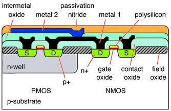
15 MOS Layout Structure Layout cross section MOS Layout Structure Schematic L: hannel Length W: hannel Width oth n channel (NMOS) and p channel (PMOS) transistors are built on the same chip substrate Well: special region created in which the semiconductor type is opposite the substrate s type Example: n well MOS fabrication technology to create a n type substrate inside the already p type substrate The n well is used to create the PMOS transistors Start from the bottom up uild the n and p type material areas on the silicon Lay the insulator layer (oxide) over the silicon Place the polysilicon (gate) on top of the oxide onnect wires to the source, gate, and drain use layers of metal above the gate Layers Layers of Metal Wires Transistor 1 Transistor 2 Side View Transistor 1 Transistor 2 Top View Photolithography n I consists of several layers of material that are manufactured in successive steps Lithography is used to selectively process the layers where the 2 mask geometry is copied on the surface Once the desired shape is patterned with photoresist the unprotected areas are etched away Lift off and etching are different techniques to remove and shape
16 Photolithography Photolithography Expose only specific areas of the chip for layer deposition or etching layer of photoresist material is deposited on the chip Photoresist becomes soluble when exposed to ultraviolet light Using a mask to cast a shadow, some portions of photoresist can be kept while the remainder is washed away Photoresist covering silicon surface Expose only specific areas of the chip for layer deposition or etching layer of photoresist material is deposited on the chip Photoresist becomes soluble when exposed to ultraviolet light Using a mask to cast a shadow, some portions of photoresist can be kept while the remainder is washed away Ultraviolet Light Exposed area will become soluble and be washed away exposing the surface underneath Mask creating shadow Photoresist covering silicon surface Masked area will stay hardened and protect the surface underneath Ion Implantation Resulting Material fter washing away soluble photoresist, silicon in the shape of the mask is exposed an be implanted with ions to make n or p type material Exposed area can now be implanted with dopants Ion source bombards the exposed silicon Photoresist covering silicon surface Surface still covered by photoresist will be protected from ion implantation fter implantation, remaining photoresist can be exposed and washed away leaving n type silicon in the appropriate areas ntype doped silicon
17 Layer eposition Layer eposition For layers above the surface (oxide, gate polysilicon, and metal wires), a similar but slightly different process is used 1. Entire layer of material is deposited over entire area 2. overed with photoresist 3. Mask is used to indicate where material is desired Ultraviolet Light Photoresist layer is placed on top Mask desired material areas For layers above the surface (oxide, gate polysilicon, and metal wires), a similar but slightly different process is used 1. Entire layer of material is deposited over entire chip 2. overed with photoresist 3. Mask is used to indicate where material is desired 4. Wash away exposed photoresist 5. Use chemical/mechanical etching process to remove exposed oxide Etching process removes exposed oxide material but cannot penetrate photoresist material Oxide layer placed over entire chip area Oxide layer placed over entire chip area Layer eposition Layer eposition For layers above the surface (oxide, gate polysilicon, and metal wires), a similar but slightly different process is used 1. Entire layer of material is deposited over entire chip 2. overed with photoresist 3. Mask is used to indicate where material is desired 4. Wash away exposed photoresist 5. Use chemical/mechanical etching process to remove exposed oxide 6. Remaining photoresist can be removed exposing oxide in the desired location Oxide layer for gate input Process is repeated for gate (polysilicon) and metal wire layers separate mask is required for each layer to indicate where the substance should be kept and where it should be etched away


18 Simplified MOS Fabrication Process Fabrication Images mageservice/rticleimage/2003/n/b208563c/b208563cf1.gif 69
Spiral Content Mapping. Spiral 1 / Unit 8. Outcomes DEMORGAN'S THEOREM. Transistor Implementations CMOS Logic Gates
 18.1 18.2 Spiral ontent Mapping Spiral Theory ombinational esign Sequential esign System Level esign Implementation and Tools Project Spiral 1 / Unit 8 Transistor Implementations MOS Logic Gates Performance
Spiral 1 / Unit 8. Transistor Implementations CMOS Logic Gates
 18.1 Spiral 1 / Unit 8 Transistor Implementations CMOS Logic Gates 18.2 Spiral Content Mapping Spiral Theory Combinational Design Sequential Design System Level Design Implementation and Tools Project
VLSI Design. Introduction
 VLSI Design Introduction Outline Introduction Silicon, pn-junctions and transistors A Brief History Operation of MOS Transistors CMOS circuits Fabrication steps for CMOS circuits Introduction Integrated
VLSI Design. Introduction
 Tassadaq Hussain VLSI Design Introduction Outcome of this course Problem Aims Objectives Outcomes Data Collection Theoretical Model Mathematical Model Validate Development Analysis and Observation Pseudo
+1 (479)
") Introduction to VLSI Design http://csce.uark.edu +1 (479) 575-6043 yrpeng@uark.edu Invention of the Transistor Vacuum tubes ruled in first half of 20th century Large, expensive, power-hungry, unreliable
Introduction to VLSI Design http://csce.uark.edu +1 (479) 575-6043 yrpeng@uark.edu Invention of the Transistor Vacuum tubes ruled in first half of 20th century Large, expensive, power-hungry, unreliable
420 Intro to VLSI Design
 Dept of Electrical and Computer Engineering 420 Intro to VLSI Design Lecture 0: Course Introduction and Overview Valencia M. Joyner Spring 2005 Getting Started Syllabus About the Instructor Labs, Problem
EE4800 CMOS Digital IC Design & Analysis. Lecture 1 Introduction Zhuo Feng
 EE4800 CMOS Digital IC Design & Analysis Lecture 1 Introduction Zhuo Feng 1.1 Prof. Zhuo Feng Office: EERC 730 Phone: 487-3116 Email: zhuofeng@mtu.edu Class Website http://www.ece.mtu.edu/~zhuofeng/ee4800fall2010.html
Lecture 0: Introduction
 Lecture 0: Introduction Introduction Integrated circuits: many transistors on one chip. Very Large Scale Integration (VLSI): bucketloads! Complementary Metal Oxide Semiconductor Fast, cheap, low power
ENG2410 Digital Design CMOS Technology. Fall 2017 S. Areibi School of Engineering University of Guelph
 ENG2410 Digital Design CMOS Technology Fall 2017 S. reibi School of Engineering University of Guelph The Transistor Revolution First transistor Bell Labs, 1948 Bipolar logic 1960 s Intel 4004 processor
Learning Outcomes. Spiral 2-6. Current, Voltage, & Resistors DIODES
 26.1 26.2 Learning Outcomes Spiral 26 Semiconductor Material MOS Theory I underst why a diode conducts current under forward bias but does not under reverse bias I underst the three modes of operation
Layers. Layers. Layers. Transistor Manufacturing COMP375 1
 VLSI COMP375 Computer Architecture Middleware other CS classes Machine Language Microcode Logic circuits Transistors Middleware Machine Language - earlier Microcode Logic circuits Transistors Middleware
Topic 3. CMOS Fabrication Process
 Topic 3 CMOS Fabrication Process Peter Cheung Department of Electrical & Electronic Engineering Imperial College London URL: www.ee.ic.ac.uk/pcheung/ E-mail: p.cheung@ic.ac.uk Lecture 3-1 Layout of a Inverter
EE 5611 Introduction to Microelectronic Technologies Fall Thursday, September 04, 2014 Lecture 02
 EE 5611 Introduction to Microelectronic Technologies Fall 2014 Thursday, September 04, 2014 Lecture 02 1 Lecture Outline Review on semiconductor materials Review on microelectronic devices Example of microelectronic
Layout of a Inverter. Topic 3. CMOS Fabrication Process. The CMOS Process - photolithography (2) The CMOS Process - photolithography (1) v o.
 The CMOS Process - photolithography (1) v o.") Layout of a Inverter Topic 3 CMOS Fabrication Process V DD Q p Peter Cheung Department of Electrical & Electronic Engineering Imperial College London v i v o Q n URL: www.ee.ic.ac.uk/pcheung/ E-mail: p.cheung@ic.ac.uk
Layout of a Inverter Topic 3 CMOS Fabrication Process V DD Q p Peter Cheung Department of Electrical & Electronic Engineering Imperial College London v i v o Q n URL: www.ee.ic.ac.uk/pcheung/ E-mail: p.cheung@ic.ac.uk
CMOS Digital Integrated Circuits Lec 2 Fabrication of MOSFETs
 CMOS Digital Integrated Circuits Lec 2 Fabrication of MOSFETs 1 CMOS Digital Integrated Circuits 3 rd Edition Categories of Materials Materials can be categorized into three main groups regarding their
Unit 3 Digital Circuits (Logic)
") Unit 3 Digital Circuits (Logic) 1 2 A Brief History COMPUTERS AND SWITCHING TECHNOLOGY 3 Mechanical Computers Primarily gearbased Difference Engine and Analytic Engine designed and partially implemented
Unit 3 Digital Circuits (Logic) 1 2 A Brief History COMPUTERS AND SWITCHING TECHNOLOGY 3 Mechanical Computers Primarily gearbased Difference Engine and Analytic Engine designed and partially implemented
Layers. Layers. Layers. Transistor Manufacturing COMP375 1
 Layers VLSI COMP370 Intro to Computer Architecture t Applications Middleware other CS classes High level languages Machine Language Microcode Logic circuits Gates Transistors Silicon structures Layers
Basic Fabrication Steps
 Basic Fabrication Steps and Layout Somayyeh Koohi Department of Computer Engineering Adapted with modifications from lecture notes prepared by author Outline Fabrication steps Transistor structures Transistor
CMOS Technology. 1. Why CMOS 2. Qualitative MOSFET model 3. Building a MOSFET 4. CMOS logic gates. Handouts: Lecture Slides. metal ndiff.
 CMOS Technology 1. Why CMOS 2. Qualitative MOSFET model 3. Building a MOSFET 4. CMOS logic gates poly pdiff metal ndiff Handouts: Lecture Slides L03 - CMOS Technology 1 Building Bits from Atoms V in V
INTRODUCTION TO MOS TECHNOLOGY
 INTRODUCTION TO MOS TECHNOLOGY 1. The MOS transistor The most basic element in the design of a large scale integrated circuit is the transistor. For the processes we will discuss, the type of transistor
Transistor was first invented by William.B.Shockley, Walter Brattain and John Bardeen of Bell Labratories. In 1961, first IC was introduced.
 Unit 1 Basic MOS Technology Transistor was first invented by William.B.Shockley, Walter Brattain and John Bardeen of Bell Labratories. In 1961, first IC was introduced. Levels of Integration:- i) SSI:-
FABRICATION OF CMOS INTEGRATED CIRCUITS. Dr. Mohammed M. Farag
 FABRICATION OF CMOS INTEGRATED CIRCUITS Dr. Mohammed M. Farag Outline Overview of CMOS Fabrication Processes The CMOS Fabrication Process Flow Design Rules Reference: Uyemura, John P. "Introduction to
Design cycle for MEMS
 Design cycle for MEMS Design cycle for ICs IC Process Selection nmos CMOS BiCMOS ECL for logic for I/O and driver circuit for critical high speed parts of the system The Real Estate of a Wafer MOS Transistor
Chapter 3: Basics Semiconductor Devices and Processing 2006/9/27 1. Topics
 Chapter 3: Basics Semiconductor Devices and Processing 2006/9/27 1 Topics What is semiconductor Basic semiconductor devices Basics of IC processing CMOS technologies 2006/9/27 2 1 What is Semiconductor
Semiconductor Physics and Devices
 Metal-Semiconductor and Semiconductor Heterojunctions The Metal-Oxide-Semiconductor Field-Effect Transistor (MOSFET) is one of two major types of transistors. The MOSFET is used in digital circuit, because
ECE 5745 Complex Digital ASIC Design Topic 2: CMOS Devices
 ECE 5745 Complex Digital ASIC Design Topic 2: CMOS Devices Christopher Batten School of Electrical and Computer Engineering Cornell University http://www.csl.cornell.edu/courses/ece5950 Simple Transistor
CS8803: Advanced Digital Design for Embedded Hardware
 HPTER II-6 MO MO WITHE WITH NETWORK -WITHE IN ERIE -WITHE IN PRLLEL -INPUT ELETOR 883: dvanced Digital Design for Embedded Hardware Lecture : MO Transistors and Layout The idea is to use the series and
Notes. (Subject Code: 7EC5)
") COMPUCOM INSTITUTE OF TECHNOLOGY & MANAGEMENT, JAIPUR (DEPARTMENT OF ELECTRONICS & COMMUNICATION) Notes VLSI DESIGN NOTES (Subject Code: 7EC5) Prepared By: MANVENDRA SINGH Class: B. Tech. IV Year, VII
COMPUCOM INSTITUTE OF TECHNOLOGY & MANAGEMENT, JAIPUR (DEPARTMENT OF ELECTRONICS & COMMUNICATION) Notes VLSI DESIGN NOTES (Subject Code: 7EC5) Prepared By: MANVENDRA SINGH Class: B. Tech. IV Year, VII
VLSI Design. Static CMOS Logic
 VLSI esign Static MOS Logic [dapted from Rabaey s igital Integrated ircuits, 2002, J. Rabaey et al.] EE4121 Static MOS Logic.1 ZLM Review: MOS Process at a Glance efine active areas Etch and fill trenches
Chapter 3 Basics Semiconductor Devices and Processing
 Chapter 3 Basics Semiconductor Devices and Processing 1 Objectives Identify at least two semiconductor materials from the periodic table of elements List n-type and p-type dopants Describe a diode and
Student Lecture by: Giangiacomo Groppi Joel Cassell Pierre Berthelot September 28 th 2004
 Student Lecture by: Giangiacomo Groppi Joel Cassell Pierre Berthelot September 28 th 2004 Lecture outline Historical introduction Semiconductor devices overview Bipolar Junction Transistor (BJT) Field
ECE 2300 Digital Logic & Computer Organization
 ECE 2300 Digital Logic & Computer Organization Spring 2018 CMOS Logic Lecture 4: 1 NAND Logic Gate X Y (X Y) = NAND Using De Morgan s Law: (X Y) = X +Y X X X +Y = Y Y Also a NAND We can build circuits
Lecture 0: Introduction
 Introduction to CMOS VLSI Design Lecture : Introduction David Harris Steven Levitan Harvey Mudd College University of Pittsburgh Spring 24 Fall 28 Administrivia Professor Steven Levitan TA: Bo Zhao Syllabus
Newer process technology (since 1999) includes :
 includes :") Newer process technology (since 1999) includes : copper metalization hi-k dielectrics for gate insulators si on insulator strained silicon lo-k dielectrics for interconnects Immersion lithography for masks
Newer process technology (since 1999) includes : copper metalization hi-k dielectrics for gate insulators si on insulator strained silicon lo-k dielectrics for interconnects Immersion lithography for masks
EMT 251 Introduction to IC Design
 EMT 251 Introduction to IC Design (Pengantar Rekabentuk Litar Terkamir) Semester II 2011/2012 Introduction to IC design and Transistor Fundamental Some Keywords! Very-large-scale-integration (VLSI) is
Semiconductor Diodes
 Semiconductor Diodes A) Motivation and Game Plan B) Semiconductor Doping and Conduction C) Diode Structure and I vs. V D) Diode Circuits Reading: Schwarz and Oldham, Chapter 13.1-13.2 Motivation Digital
Learning Outcomes. Spiral 2 8. Digital Design Overview LAYOUT
 2-8.1 2-8.2 Spiral 2 8 Cell Mark Redekopp earning Outcomes I understand how a digital circuit is composed of layers of materials forming transistors and wires I understand how each layer is expressed as
EECS 151/251A Spring 2019 Digital Design and Integrated Circuits. Instructors: Wawrzynek. Lecture 8 EE141
 EECS 151/251A Spring 2019 Digital Design and Integrated Circuits Instructors: Wawrzynek Lecture 8 EE141 From the Bottom Up IC processing CMOS Circuits (next lecture) EE141 2 Overview of Physical Implementations
2009 Spring CS211 Digital Systems & Lab 1 CHAPTER 3: TECHNOLOGY (PART 2)
") 1 CHAPTER 3: IMPLEMENTATION TECHNOLOGY (PART 2) Whatwillwelearninthischapter? we learn in this 2 How transistors operate and form simple switches CMOS logic gates IC technology FPGAs and other PLDs Basic
1 CHAPTER 3: IMPLEMENTATION TECHNOLOGY (PART 2) Whatwillwelearninthischapter? we learn in this 2 How transistors operate and form simple switches CMOS logic gates IC technology FPGAs and other PLDs Basic
TECHNO INDIA BATANAGAR (DEPARTMENT OF ELECTRONICS & COMMUNICATION ENGINEERING) QUESTION BANK- 2018
 QUESTION BANK- 2018") TECHNO INDIA BATANAGAR (DEPARTMENT OF ELECTRONICS & COMMUNICATION ENGINEERING) QUESTION BANK- 2018 Paper Setter Detail Name Designation Mobile No. E-mail ID Raina Modak Assistant Professor 6290025725 raina.modak@tib.edu.in
TECHNO INDIA BATANAGAR (DEPARTMENT OF ELECTRONICS & COMMUNICATION ENGINEERING) QUESTION BANK- 2018 Paper Setter Detail Name Designation Mobile No. E-mail ID Raina Modak Assistant Professor 6290025725 raina.modak@tib.edu.in
MICROPROCESSOR TECHNOLOGY
 MICROPROCESSOR TECHNOLOGY Assis. Prof. Hossam El-Din Moustafa Lecture 3 Ch.1 The Evolution of The Microprocessor 17-Feb-15 1 Chapter Objectives Introduce the microprocessor evolution from transistors to
PHYS 3050 Electronics I
 PHYS 3050 Electronics I Chapter 4. Semiconductor Diodes and Transistors Earth, Moon, Mars, and Beyond Dr. Jinjun Shan, Associate Professor of Space Engineering Department of Earth and Space Science and
Module-3: Metal Oxide Semiconductor (MOS) & Emitter coupled logic (ECL) families
 & Emitter coupled logic (ECL) families") 1 Module-3: Metal Oxide Semiconductor (MOS) & Emitter coupled logic (ECL) families 1. Introduction 2. Metal Oxide Semiconductor (MOS) logic 2.1. Enhancement and depletion mode 2.2. NMOS and PMOS inverter
1 Module-3: Metal Oxide Semiconductor (MOS) & Emitter coupled logic (ECL) families 1. Introduction 2. Metal Oxide Semiconductor (MOS) logic 2.1. Enhancement and depletion mode 2.2. NMOS and PMOS inverter
Physical Structure of CMOS Integrated Circuits
 Physical Structure of CMOS Integrated Circuits Dae Hyun Kim EECS Washington State University References John P. Uyemura, Introduction to VLSI Circuits and Systems, 2002. Chapter 3 Neil H. Weste and David
BICMOS Technology and Fabrication
 12-1 BICMOS Technology and Fabrication 12-2 Combines Bipolar and CMOS transistors in a single integrated circuit By retaining benefits of bipolar and CMOS, BiCMOS is able to achieve VLSI circuits with
EE 42/100 Lecture 23: CMOS Transistors and Logic Gates. Rev A 4/15/2012 (10:39 AM) Prof. Ali M. Niknejad
 Prof. Ali M. Niknejad") A. M. Niknejad University of California, Berkeley EE 100 / 42 Lecture 23 p. 1/16 EE 42/100 Lecture 23: CMOS Transistors and Logic Gates ELECTRONICS Rev A 4/15/2012 (10:39 AM) Prof. Ali M. Niknejad University
A. M. Niknejad University of California, Berkeley EE 100 / 42 Lecture 23 p. 1/16 EE 42/100 Lecture 23: CMOS Transistors and Logic Gates ELECTRONICS Rev A 4/15/2012 (10:39 AM) Prof. Ali M. Niknejad University
Microelectronics, BSc course
 Microelectronics, BSc course MOS circuits: CMOS circuits, construction http://www.eet.bme.hu/~poppe/miel/en/14-cmos.pptx http://www.eet.bme.hu The abstraction level of our study: SYSTEM + MODULE GATE CIRCUIT
VLSI DESIGN AUTOMATION COURSE NOTES THE PRINCIPLES OF VLSI DESIGN
 VLSI DESIGN AUTOMATION COURSE NOTES THE PRINCIPLES OF VLSI DESIGN Peter M. Maurer ENG 118 Department of Computer Science & Engineering University of South Florida Tampa, FL 33620 1. The Nature of licon
EC0306 INTRODUCTION TO VLSI DESIGN
 EC0306 INTRODUCTION TO VLSI DESIGN UNIT I INTRODUCTION TO MOS CIRCUITS Why VLSI? Integration improves the design: o lower parasitics = higher speed; o lower power; o physically smaller. Integration reduces
Integrated diodes. The forward voltage drop only slightly depends on the forward current. ELEKTRONIKOS ĮTAISAI
 1 Integrated diodes pn junctions of transistor structures can be used as integrated diodes. The choice of the junction is limited by the considerations of switching speed and breakdown voltage. The forward
MOSFETS: Gain & non-linearity
 MOFET: ain & non-linearity source gate Polysilicon wire Heavily doped (n-type or p-type) diffusions W Inter-layer io 2 insulation Very thin (
Lecture # 23 Diodes and Diode Circuits. A) Basic Semiconductor Materials B) Diode Current and Equation C) Diode Circuits
 Basic Semiconductor Materials B) Diode Current and Equation C) Diode Circuits") EECS 42 ntro. Digital Electronics, Fall 2003 EECS 42 ntroduction to Digital Electronics Lecture # 23 Diodes and Diode Circuits A) Basic Semiconductor Materials B) Diode Current and Equation C) Diode Circuits
EECS 42 ntro. Digital Electronics, Fall 2003 EECS 42 ntroduction to Digital Electronics Lecture # 23 Diodes and Diode Circuits A) Basic Semiconductor Materials B) Diode Current and Equation C) Diode Circuits
Mathematics and Science in Schools in Sub-Saharan Africa
 Mathematics and Science in Schools in Sub-Saharan Africa SEMICONDUCTORS What is a Semiconductor? What is a Semiconductor? Microprocessors LED Transistors Capacitors Range of Conduciveness The semiconductors
2.8 - CMOS TECHNOLOGY
 CMOS Technology (6/7/00) Page 1 2.8 - CMOS TECHNOLOGY INTRODUCTION Objective The objective of this presentation is: 1.) Illustrate the fabrication sequence for a typical MOS transistor 2.) Show the physical
APPLICATION TRAINING GUIDE
 APPLICATION TRAINING GUIDE Basic Semiconductor Theory Semiconductor is an appropriate name for the device because it perfectly describes the material from which it's made -- not quite a conductor, and
UNIT-VI FIELD EFFECT TRANSISTOR. 1. Explain about the Field Effect Transistor and also mention types of FET s.
 UNIT-I FIELD EFFECT TRANSISTOR 1. Explain about the Field Effect Transistor and also mention types of FET s. The Field Effect Transistor, or simply FET however, uses the voltage that is applied to their
The Design and Realization of Basic nmos Digital Devices
 Proceedings of The National Conference On Undergraduate Research (NCUR) 2004 Indiana University Purdue University Indianapolis, Indiana April 15-17, 2004 The Design and Realization of Basic nmos Digital
Logic Design (Part 1) Transistors & Gates (Chapter 3)
 Transistors & Gates (Chapter 3)") Agenda next 3 weeks: Inside a microprocessor Logic Design (Part 1) Transistors & Gates (Chapter 3) Based on slides McGrawHill Additional material 2004/2005/2006 Lewis/Martin Additional material 2008 Roth
Agenda next 3 weeks: Inside a microprocessor Logic Design (Part 1) Transistors & Gates (Chapter 3) Based on slides McGrawHill Additional material 2004/2005/2006 Lewis/Martin Additional material 2008 Roth
ECE520 VLSI Design. Lecture 2: Basic MOS Physics. Payman Zarkesh-Ha
 ECE520 VLSI Design Lecture 2: Basic MOS Physics Payman Zarkesh-Ha Office: ECE Bldg. 230B Office hours: Wednesday 2:00-3:00PM or by appointment E-mail: pzarkesh@unm.edu Slide: 1 Review of Last Lecture Semiconductor
Lecture 4 - Digital Representations III + Transistors
 Lecture 4 - Digital Representations III + Transistors Video: Seems like a natural extension from images no? We just have a new dimension (time) Each frame is just an image made up of pixels Display n frames
UNIT III VLSI CIRCUIT DESIGN PROCESSES. In this chapter we will be studying how to get the schematic into stick diagrams or layouts.
 UNIT III VLSI CIRCUIT DESIGN PROCESSES In this chapter we will be studying how to get the schematic into stick diagrams or layouts. MOS circuits are formed on four basic layers: N-diffusion P-diffusion
Introduction to VLSI ASIC Design and Technology
 Introduction to VLSI ASIC Design and Technology Paulo Moreira CERN - Geneva, Switzerland Paulo Moreira Introduction 1 Outline Introduction Is there a limit? Transistors CMOS building blocks Parasitics
Shorthand Notation for NMOS and PMOS Transistors
 Shorthand Notation for NMOS and PMOS Transistors Terminal Voltages Mode of operation depends on V g, V d, V s V gs = V g V s V gd = V g V d V ds = V d V s = V gs - V gd Source and drain are symmetric diffusion
Improved Inverter: Current-Source Pull-Up. MOS Inverter with Current-Source Pull-Up. What else could be connected between the drain and V DD?
 Improved Inverter: Current-Source Pull-Up MOS Inverter with Current-Source Pull-Up What else could be connected between the drain and? Replace resistor with current source I SUP roc i D v IN v OUT Find
EECE 481. MOS Basics Lecture 2
 EECE 481 MOS Basics Lecture 2 Reza Molavi Dept. of ECE University of British Columbia reza@ece.ubc.ca Slides Courtesy : Dr. Res Saleh (UBC), Dr. D. Sengupta (AMD), Dr. B. Razavi (UCLA) 1 PN Junction and
ECE 334: Electronic Circuits Lecture 10: Digital CMOS Circuits
 Faculty of Engineering ECE 334: Electronic Circuits Lecture 10: Digital CMOS Circuits CMOS Technology Complementary MOS, or CMOS, needs both PMOS and NMOS FET devices for their logic gates to be realized
Unit-1. MOS Transistor Theory
 VLSI DESIGN -EEE Unit-1 MOS Transistor Theory VLSI DESIGN UNIT I Contents: 1.1 Historical Perspective 1.2 What is VLSI? - Introduction 1.3 VLSI Design Flow 1.4 Design Hierarchy 1.5 Basic MOS Transistor
Intro to Electricity. Introduction to Transistors. Example Circuit Diagrams. Water Analogy
 Introduction to Transistors Transistors form the basic building blocks of all computer hardware. Invented by William Shockley, John Bardeen and Walter Brattain in 1947, replacing previous vaccuumtube technology
Digital Systems Laboratory
 2012 Fall CSE140L Digital Systems Laboratory Lecture #2 by Dr. Choon Kim CSE Department, UCSD chk034@eng.ucsd.edu Lecture #2 1 Digital Technologies CPU(Central Processing Unit) GPU(Graphics Processing
Semiconductor Devices
 Semiconductor Devices - 2014 Lecture Course Part of SS Module PY4P03 Dr. P. Stamenov School of Physics and CRANN, Trinity College, Dublin 2, Ireland Hilary Term, TCD 3 th of Feb 14 MOSFET Unmodified Channel
EE 330 Lecture 7. Design Rules. IC Fabrication Technology Part 1
 EE 330 Lecture 7 Design Rules IC Fabrication Technology Part 1 Review from Last Time Technology Files Provide Information About Process Process Flow (Fabrication Technology) Model Parameters Design Rules
Introduction. Reading: Chapter 1. Courtesy of Dr. Dansereau, Dr. Brown, Dr. Vranesic, Dr. Harris, and Dr. Choi.
 Introduction Reading: Chapter 1 Courtesy of Dr. Dansereau, Dr. Brown, Dr. Vranesic, Dr. Harris, and Dr. Choi http://csce.uark.edu +1 (479) 575-6043 yrpeng@uark.edu Why study logic design? Obvious reasons
ECE380 Digital Logic. Logic values as voltage levels
 ECE380 Digital Logic Implementation Technology: NMOS and PMOS Transistors, CMOS logic gates Dr. D. J. Jackson Lecture 13-1 Logic values as voltage levels V ss is the minimum voltage that can exist in the
ECE520 VLSI Design. Lecture 11: Combinational Static Logic. Prof. Payman Zarkesh-Ha
 EE520 VLSI esign Lecture 11: ombinational Static Logic Prof. Payman Zarkesh-Ha Office: EE ldg. 230 Office hours: Wednesday 2:00-3:00PM or by appointment E-mail: pzarkesh@unm.edu Slide: 1 eview of Last
Chapter 3. H/w s/w interface. hardware software Vijaykumar ECE495K Lecture Notes: Chapter 3 1
 Chapter 3 hardware software H/w s/w interface Problems Algorithms Prog. Lang & Interfaces Instruction Set Architecture Microarchitecture (Organization) Circuits Devices (Transistors) Bits 29 Vijaykumar
Computer Architecture (TT 2012)
") Computer Architecture (TT 212) Laws of Attraction aniel Kroening Oxford University, Computer Science epartment Version 1., 212 . Kroening: Computer Architecture (TT 212) 2 . Kroening: Computer Architecture
Computer Architecture (TT 212) Laws of Attraction aniel Kroening Oxford University, Computer Science epartment Version 1., 212 . Kroening: Computer Architecture (TT 212) 2 . Kroening: Computer Architecture
DIGITAL TECHNICS II. Dr. Bálint Pődör. Óbuda University, Microelectronics and Technology Institute 7. LECTURE: LOGIC CIRCUITS II: FET, MOS AND CMOS
 DIGITL TECHNICS II Dr. álint Pődör Óbuda University, Microelectronics and Technology Institute 7. LECTURE: LOGIC CIRCUITS II: FET, MOS ND CMOS 2nd (Spring) term 2015/2016 1 7. LECTURE: LOGIC CIRCUITS II:
EECS130 Integrated Circuit Devices
 EECS130 Integrated Circuit Devices Professor Ali Javey 11/6/2007 MOSFETs Lecture 6 BJTs- Lecture 1 Reading Assignment: Chapter 10 More Scalable Device Structures Vertical Scaling is important. For example,
PAPER SOLUTION_DECEMBER_2014_VLSI_DESIGN_ETRX_SEM_VII Prepared by Girish Gidaye
 Q1a) The MOS System under External Bias Depending on the polarity and the magnitude of V G, three different operating regions can be observed for the MOS system: 1) Accumulation 2) Depletion 3) Inversion
VLSI Designed Low Power Based DPDT Switch
 International Journal of Electronics and Communication Engineering. ISSN 0974-2166 Volume 8, Number 1 (2015), pp. 81-86 International Research Publication House http://www.irphouse.com VLSI Designed Low
Chapter 2 : Semiconductor Materials & Devices (II) Feb
 Feb") Chapter 2 : Semiconductor Materials & Devices (II) 1 Reference 1. SemiconductorManufacturing Technology: Michael Quirk and Julian Serda (2001) 3. Microelectronic Circuits (5/e): Sedra & Smith (2004) 4.
Chapter 2 : Semiconductor Materials & Devices (II) 1 Reference 1. SemiconductorManufacturing Technology: Michael Quirk and Julian Serda (2001) 3. Microelectronic Circuits (5/e): Sedra & Smith (2004) 4.
Chapter 1, Introduction
 Introduction to Semiconductor Manufacturing Technology Chapter 1, Introduction hxiao89@hotmail.com 1 Objective After taking this course, you will able to Use common semiconductor terminology Describe a
Design Simulation and Analysis of NMOS Characteristics for Varying Oxide Thickness
 MIT International Journal of Electronics and Communication Engineering, Vol. 4, No. 2, August 2014, pp. 81 85 81 Design Simulation and Analysis of NMOS Characteristics for Varying Oxide Thickness Alpana
Reading. Lecture 17: MOS transistors digital. Context. Digital techniques:
 Reading Lecture 17: MOS transistors digital Today we are going to look at the analog characteristics of simple digital devices, 5. 5.4 And following the midterm, we will cover PN diodes again in forward
CHAPTER FORMULAS & NOTES
 Formulae For u SEMICONDUCTORS By Mir Mohammed Abbas II PCMB 'A' 1 Important Terms, Definitions & Formulae CHAPTER FORMULAS & NOTES 1 Intrinsic Semiconductor: The pure semiconductors in which the electrical
Power Bipolar Junction Transistors (BJTs)
") ECE442 Power Semiconductor Devices and Integrated Circuits Power Bipolar Junction Transistors (BJTs) Zheng Yang (ERF 3017, email: yangzhen@uic.edu) Power Bipolar Junction Transistor (BJT) Background The
ECE442 Power Semiconductor Devices and Integrated Circuits Power Bipolar Junction Transistors (BJTs) Zheng Yang (ERF 3017, email: yangzhen@uic.edu) Power Bipolar Junction Transistor (BJT) Background The
INTRODUCTION: Basic operating principle of a MOSFET:
 INTRODUCTION: Along with the Junction Field Effect Transistor (JFET), there is another type of Field Effect Transistor available whose Gate input is electrically insulated from the main current carrying
Review: CMOS Logic Gates
 Review: CMOS Logic Gates INV Schematic NOR Schematic NAND Schematic + Vsg - pmos x x Vin Vout = Vin y + Vgs - nmos CMOS inverts functions CMOS Combinational Logic x g(x,y) = x + y use DeMorgan relations
Power MOSFET Zheng Yang (ERF 3017,
 ECE442 Power Semiconductor Devices and Integrated Circuits Power MOSFET Zheng Yang (ERF 3017, email: yangzhen@uic.edu) Evolution of low-voltage (
Lecture Integrated circuits era
 Lecture 1 1.1 Integrated circuits era Transistor was first invented by William.B.Shockley, Walter Brattain and John Bardeen of Bell laboratories. In 1961, first IC was introduced. Levels of Integration:-
Three Terminal Devices
 Three Terminal Devices - field effect transistor (FET) - bipolar junction transistor (BJT) - foundation on which modern electronics is built - active devices - devices described completely by considering
College of Engineering Department of Electrical Engineering and Computer Sciences University of California, Berkeley
 College of Engineering Department of Electrical Engineering and Below are your weekly quizzes. You should print out a copy of the quiz and complete it before your lab section. Bring in the completed quiz
From Sand to Silicon Making of a Chip Illustrations May 2009
 From Sand to Silicon Making of a Chip Illustrations May 2009 1 The illustrations on the following foils are low resolution images that visually support the explanations of the individual steps. For publishing
ECE/CoE 0132: FETs and Gates
 ECE/CoE 0132: FETs and Gates Kartik Mohanram September 6, 2017 1 Physical properties of gates Over the next 2 lectures, we will discuss some of the physical characteristics of integrated circuits. We will
VLSI Technology Dr. Nandita Dasgupta Department of Electrical Engineering Indian Institute of Technology, Madras
 VLSI Technology Dr. Nandita Dasgupta Department of Electrical Engineering Indian Institute of Technology, Madras Lecture - 39 Latch up in CMOS We have been discussing about the problems in CMOS, basic
Progress due to: Feature size reduction - 0.7X/3 years (Moore s Law). Increasing chip size - 16% per year. Creativity in implementing functions.
. Increasing chip size - 16% per year. Creativity in implementing functions.") Introduction - Chapter 1 Evolution of IC Fabrication 1960 and 1990 integrated t circuits. it Progress due to: Feature size reduction - 0.7X/3 years (Moore s Law). Increasing chip size - 16% per year. Creativity
Introduction - Chapter 1 Evolution of IC Fabrication 1960 and 1990 integrated t circuits. it Progress due to: Feature size reduction - 0.7X/3 years (Moore s Law). Increasing chip size - 16% per year. Creativity
Basic Electronics: Diodes and Transistors. October 14, 2005 ME 435
 Basic Electronics: Diodes and Transistors Eşref Eşkinat E October 14, 2005 ME 435 Electric lectricity ity to Electronic lectronics Electric circuits are connections of conductive wires and other devices
Major Fabrication Steps in MOS Process Flow
 Major Fabrication Steps in MOS Process Flow UV light Mask oxygen Silicon dioxide photoresist exposed photoresist oxide Silicon substrate Oxidation (Field oxide) Photoresist Coating Mask-Wafer Alignment
EE301 Electronics I , Fall
 EE301 Electronics I 2018-2019, Fall 1. Introduction to Microelectronics (1 Week/3 Hrs.) Introduction, Historical Background, Basic Consepts 2. Rewiev of Semiconductors (1 Week/3 Hrs.) Semiconductor materials
Intel s High-k/Metal Gate Announcement. November 4th, 2003
 Intel s High-k/Metal Gate Announcement November 4th, 2003 1 What are we announcing? Intel has made significant progress in future transistor materials Two key parts of this new transistor are: The gate