ECE 471/571 Combinatorial Circuits Lecture-7. Gurjeet Singh
|
|
|
- Bathsheba Angelica Bennett
- 6 years ago
- Views:
Transcription
1 ECE 471/571 Combinatorial Circuits Lecture-7 Gurjeet Singh
2 Propagation Delay of CMOS Gates
3 Propagation delay of Four input NAND Gate
4 Disadvantages of Complementary CMOS Design Increase in complexity Larger implementation area Propagation delay deteriorates rapidly as a function of fan-in
5 Disadvantages of Complementary CMOS Design Large number of transistors increases overall capacitance of the gate Series connection causes slowdown
6 Design Techniques for Large Fan-in
7 Transistor Sizing Increase the size of transistor But increasing the transistor size also increases propagation delay
8 Progressive Transistor Sizing
9 Input Reordering
10 Logic Restructuring
11 Optimizing Performance in Combinatorial Networks tp0 = intrinsic delay of an inverter f = effective fan-out(ratio between external load and input capacitance), also called electrical effort p = ratio of intrinsic delays of the complex gates and the simple inverter. Function of gate topology as well as layout style g = logical effort
12 Estimated of p and g
13 Optimizing Performance in Combinatorial Networks gate effort h = fg
14 Optimizing Performance in Combinatorial Networks Total delay of path through combinatorial logic block Find minimum delay by finding N-1 partial derivative and set them to zero, we get Path logical effort, G can be found by multiplying logical efforts of all the gates G= gi
15 Optimizing Performance in Combinatorial Networks Path effective fan-out(or electrical effort) F, F= CL/Cg1 Some of the drive current is directed along path while some is directed of the path. We need to calculation branching effort as well b= (Con-path+Coff-path)/Con-path Path Branching effort can be calculated by B= bi
16 Optimizing Performance in Combinatorial Networks Path Electrical effort can be calculated from electrical and branching effort F = ℿ(fi/bi) = (ℿfi)/B Total path effort H can be defined as H = ℿhi = ℿgifi = GFB Gate effort that minimizes the path delay is Minimum delay of path is given by:
17 Optimizing Performance in Combinatorial Networks If s1 is the sizing factor of first gate in the chain g2s2cref = (f1/b1)g1s1cref For gate i in the chain, this yields si = (g1s1/gi)ℿi-1j=1(fj/gj)
18 Example F G B H h f1 f2 f3 f4 a b c = CL/Cg1 = 5 = 1*(5/3)*(5/3)*1 = 1 (no branching) = GFB = 4 (125/9) = 1.93 = 1.93*(3/5) = 1.16 = 1.93 = f1g1/g2 = f1f2g1/g3 = f1f2f3g1/g4 = 25/9 = 125/9 = 1.93 =1.16 =1.16 =1.34 =2.60
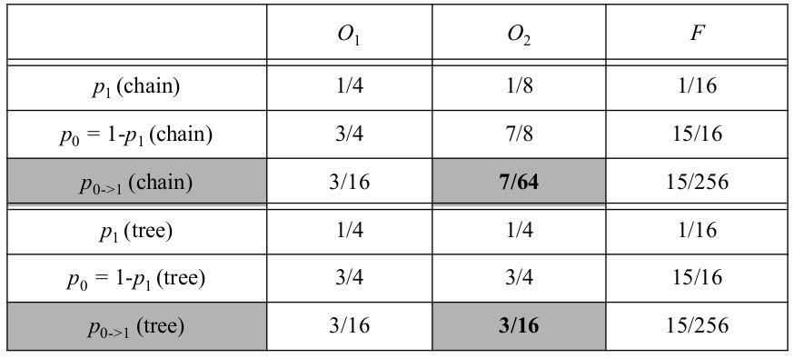
19 Power Consumption in CMOS Logic Gates Dynamic power dissipation, is switching activity Static component based on topology Dynamic component based on timing behaviour(glitching) 0->1 po is probability when output is zero p1 is probability when output is one
20 Example

21 Signal Statistics Let, pa and pb be the probabilities that the inputs A and B are one.assume inputs are not correlated. The probability the the output node is 1 is given by Probability of transition from 0 to 1 is
22 Intersignal Correlations
23 Dynamic or Glitching Transitions
24 Design Techniques to Reduce Switching Activity
25 Logic Restructuring
26 Input ordering
27 Time-multiplexing Resources
28 Glitch Reduction by balancing signal paths
29 Ratioed Logic
30 Features Lesser number of transistors compared to Complementary approach(n+1 compared to 2N) Nominal High Voltage VOH is VDD Nominal low voltage is not 0V Reduced Noise Margin Increase in static power dissipation.
31 Pseudo NMOS Inverter
32 NAND vs NOR in Pseudo-NMOS Which one would you prefer to implement in pseudo-nmos?
33 Building Better Loads Differential Logic Requires each input is provided by complementary format Positive Feedback Ensure that load device is turned off when not needed One example is Differential Cascode Voltage Switch Logic(DCVSL)
34 Single-Ended vs Differential Differential reduces number of transistors required by 2 Differential removes need for inverter stage Differential need more wires for interconnects High Dynamic power dissipation
35 Pass-Transistor Logic Advantages Fewer transistors required Disadvantages NMOS is poor in pulling a node to VDD NMOS experience body effect when pulling voltage to high
36 Voltage Swing for Pass Transistor Circuits
37 Energy of Pass-Transistor Logic
38 Differential Pass-Transistor Logic (CPL or DPL)
39 Properties of DPL Both input and output signal and its complement available. Output either connected to VDD or GND via low-resistance path Since design is almost similar. It makes it easier for modular design library
40 Robust and Efficient Pass-Transistor Design
41 Level Restoration
42 Level Restoration
43 Multiple Threshold Transistors
44 Transmission Gate Logic
ECE 471/571 The CMOS Inverter Lecture-6. Gurjeet Singh
 ECE 471/571 The CMOS Inverter Lecture-6 Gurjeet Singh NMOS-to-PMOS ratio,pmos are made β times larger than NMOS Sizing Inverters for Performance Conclusions: Intrinsic delay tp0 is independent of sizing
Topic 6. CMOS Static & Dynamic Logic Gates. Static CMOS Circuit. NMOS Transistors in Series/Parallel Connection
 NMOS Transistors in Series/Parallel Connection Topic 6 CMOS Static & Dynamic Logic Gates Peter Cheung Department of Electrical & Electronic Engineering Imperial College London Transistors can be thought
ECE 334: Electronic Circuits Lecture 10: Digital CMOS Circuits
 Faculty of Engineering ECE 334: Electronic Circuits Lecture 10: Digital CMOS Circuits CMOS Technology Complementary MOS, or CMOS, needs both PMOS and NMOS FET devices for their logic gates to be realized
EE241 - Spring 2006 Advanced Digital Integrated Circuits. Notes. Lecture 7: Logic Families for Performance
 EE241 - Spring 2006 dvanced Digital Integrated Circuits Lecture 7: Logic Families for Performance Notes Hw 1 due tomorrow Feedback on projects will be sent out by the end of the weekend Some thoughts on
CHAPTER 5 DESIGN AND ANALYSIS OF COMPLEMENTARY PASS- TRANSISTOR WITH ASYNCHRONOUS ADIABATIC LOGIC CIRCUITS
 70 CHAPTER 5 DESIGN AND ANALYSIS OF COMPLEMENTARY PASS- TRANSISTOR WITH ASYNCHRONOUS ADIABATIC LOGIC CIRCUITS A novel approach of full adder and multipliers circuits using Complementary Pass Transistor
CMOS Transistor and Circuits. Jan 2015 CMOS Transistor 1
 CMOS Transistor and Circuits Jan 2015 CMOS Transistor 1 Latchup in CMOS Circuits Jan 2015 CMOS Transistor 2 Parasitic bipolar transistors are formed by substrate and source / drain devices Latchup occurs
EEC 118 Lecture #11: CMOS Design Guidelines Alternative Static Logic Families
 EEC 118 Lecture #11: CMOS Design Guidelines Alternative Static Logic Families Rajeevan Amirtharajah University of California, Davis Jeff Parkhurst Intel Corporation Announcements Homework 5 this week Lab
EE434 ASIC & Digital Systems
 EE434 ASIC & Digital Systems Partha Pande School of EECS Washington State University pande@eecs.wsu.edu Spring 2015 Dae Hyun Kim daehyun@eecs.wsu.edu 1 Lecture 4 More on CMOS Gates Ref: Textbook chapter
EE241 - Spring 2002 Advanced Digital Integrated Circuits
 EE241 - Spring 2002 dvanced Digital Integrated Circuits Lecture 7 MOS Logic Styles nnouncements Homework #1 due 2/19 1 Reading Chapter 7 in the text by K. ernstein ackground material from Rabaey References»
CPE/EE 427, CPE 527 VLSI Design I: Homeworks 3 & 4
 CPE/EE 427, CPE 527 VLSI Design I: Homeworks 3 & 4 1 2 3 4 5 6 7 8 9 10 Sum 30 10 25 10 30 40 10 15 15 15 200 1. (30 points) Misc, Short questions (a) (2 points) Postponing the introduction of signals
Digital Microelectronic Circuits ( ) CMOS Digital Logic. Lecture 6: Presented by: Adam Teman
 CMOS Digital Logic. Lecture 6: Presented by: Adam Teman") Digital Microelectronic Circuits (361-1-3021 ) Presented by: Adam Teman Lecture 6: CMOS Digital Logic 1 Last Lectures The CMOS Inverter CMOS Capacitance Driving a Load 2 This Lecture Now that we know all
Digital Microelectronic Circuits (361-1-3021 ) Presented by: Adam Teman Lecture 6: CMOS Digital Logic 1 Last Lectures The CMOS Inverter CMOS Capacitance Driving a Load 2 This Lecture Now that we know all
Combinational Logic Gates in CMOS
 Combinational Logic Gates in CMOS References: dapted from: Digital Integrated Circuits: Design Perspective, J. Rabaey UC Principles of CMOS VLSI Design: Systems Perspective, 2nd Ed., N. H. E. Weste and
A Literature Survey on Low PDP Adder Circuits
 Available Online at www.ijcsmc.com International Journal of Computer Science and Mobile Computing A Monthly Journal of Computer Science and Information Technology IJCSMC, Vol. 4, Issue. 12, December 2015,
VLSI Logic Structures
 VLSI Logic Structures Ratioed Logic Pass-Transistor Logic Dynamic CMOS Domino Logic Zipper CMOS Spring 25 John. Chandy inary Multiplication + x Multiplicand Multiplier Partial products Result Spring 25
Chapter 6 DIFFERENT TYPES OF LOGIC GATES
 Chapter 6 DIFFERENT TYPES OF LOGIC GATES Lesson 9 CMOS gates Ch06L9-"Digital Principles and Design", Raj Kamal, Pearson Education, 2006 2 Outline CMOS (n-channel based MOSFETs based circuit) CMOS Features
Digital Microelectronic Circuits ( ) Pass Transistor Logic. Lecture 9: Presented by: Adam Teman
 Pass Transistor Logic. Lecture 9: Presented by: Adam Teman") Digital Microelectronic Circuits (361-1-3021 ) Presented by: Adam Teman Lecture 9: Pass Transistor Logic 1 Motivation In the previous lectures, we learned about Standard CMOS Digital Logic design. CMOS
Digital Microelectronic Circuits (361-1-3021 ) Presented by: Adam Teman Lecture 9: Pass Transistor Logic 1 Motivation In the previous lectures, we learned about Standard CMOS Digital Logic design. CMOS
Power-Area trade-off for Different CMOS Design Technologies
 Power-Area trade-off for Different CMOS Design Technologies Priyadarshini.V Department of ECE Sri Vishnu Engineering College for Women, Bhimavaram dpriya69@gmail.com Prof.G.R.L.V.N.Srinivasa Raju Head
Lecture 16. Complementary metal oxide semiconductor (CMOS) CMOS 1-1
 CMOS 1-1") Lecture 16 Complementary metal oxide semiconductor (CMOS) CMOS 1-1 Outline Complementary metal oxide semiconductor (CMOS) Inverting circuit Properties Operating points Propagation delay Power dissipation
Lecture 16 Complementary metal oxide semiconductor (CMOS) CMOS 1-1 Outline Complementary metal oxide semiconductor (CMOS) Inverting circuit Properties Operating points Propagation delay Power dissipation
ECE/CoE 0132: FETs and Gates
 ECE/CoE 0132: FETs and Gates Kartik Mohanram September 6, 2017 1 Physical properties of gates Over the next 2 lectures, we will discuss some of the physical characteristics of integrated circuits. We will
CMOS Circuits CONCORDIA VLSI DESIGN LAB
 CMOS Circuits 1 Combination and Sequential 2 Static Combinational Network CMOS Circuits Pull-up network-pmos Pull-down network-nmos Networks are complementary to each other When the circuit is dormant,
Module 4 : Propagation Delays in MOS Lecture 19 : Analyzing Delay for various Logic Circuits
 Module 4 : Propagation Delays in MOS Lecture 19 : Analyzing Delay for various Logic Circuits Objectives In this lecture you will learn the following Ratioed Logic Pass Transistor Logic Dynamic Logic Circuits
Chapter 6 Combinational CMOS Circuit and Logic Design. Jin-Fu Li Department of Electrical Engineering National Central University Jungli, Taiwan
 Chapter 6 Combinational CMOS Circuit and Logic Design Jin-Fu Li Department of Electrical Engineering National Central University Jungli, Taiwan Outline Advanced Reliable Systems (ARES) Lab. Jin-Fu Li,
COMPREHENSIVE ANALYSIS OF ENHANCED CARRY-LOOK AHEAD ADDER USING DIFFERENT LOGIC STYLES
 COMPREHENSIVE ANALYSIS OF ENHANCED CARRY-LOOK AHEAD ADDER USING DIFFERENT LOGIC STYLES PSowmya #1, Pia Sarah George #2, Samyuktha T #3, Nikita Grover #4, Mrs Manurathi *1 # BTech,Electronics and Communication,Karunya
EE 330 Lecture 42. Other Logic Styles Digital Building Blocks
 EE 330 Lecture 42 Other Logic Styles Digital Building Blocks Logic Styles Static CMOS Complex Logic Gates Pass Transistor Logic (PTL) Pseudo NMOS Dynamic Logic Domino Zipper Static CMOS Widely used Attractive
! Is it feasible? ! How do we decompose the problem? ! Vdd. ! Topology. " Gate choice, logical optimization. " Fanin, fanout, Serial vs.
 ESE 570: Digital Integrated Circuits and VLSI Fundamentals Design Space Exploration Lec 18: March 28, 2017 Design Space Exploration, Synchronous MOS Logic, Timing Hazards 3 Design Problem Problem Solvable!
A Low-Power High-speed Pipelined Accumulator Design Using CMOS Logic for DSP Applications
 International Journal of Research Studies in Computer Science and Engineering (IJRSCSE) Volume. 1, Issue 5, September 2014, PP 30-42 ISSN 2349-4840 (Print) & ISSN 2349-4859 (Online) www.arcjournals.org
Design of Low-Power High-Performance 2-4 and 4-16 Mixed-Logic Line Decoders
 Design of Low-Power High-Performance 2-4 and 4-16 Mixed-Logic Line Decoders B. Madhuri Dr.R. Prabhakar, M.Tech, Ph.D. bmadhusingh16@gmail.com rpr612@gmail.com M.Tech (VLSI&Embedded System Design) Vice
ECE520 VLSI Design. Lecture 5: Basic CMOS Inverter. Payman Zarkesh-Ha
 ECE520 VLSI Design Lecture 5: Basic CMOS Inverter Payman Zarkesh-Ha Office: ECE Bldg. 230B Office hours: Wednesday 2:00-3:00PM or by appointment E-mail: pzarkesh@unm.edu Slide: 1 Review of Last Lecture
r 2 ISSN Multiplier can large product bits in operation. process for Multiplication In is composed adder carry and of Tree Multiplier
 Implementation Comparison of Tree Multiplier using Different Circuit Techniques Subhag Yadav, Vipul Bhatnagar, Department of Electronics Communication, Inderprastha Engineering College, UPTU, Ghaziabad,
Digital Integrated Circuits Designing Combinational Logic Circuits. Fuyuzhuo
 Digital Integrated Circuits Designing Combinational Logic Circuits Fuyuzhuo Introduction Digital IC Ratioed Logic Introduction Digital IC EE141 2 Ratioed Logic design Basic concept Resistive load Depletion
1. Short answer questions. (30) a. What impact does increasing the length of a transistor have on power and delay? Why? (6)
 a. What impact does increasing the length of a transistor have on power and delay? Why? (6)") CSE 493/593 Test 2 Fall 2011 Solution 1. Short answer questions. (30) a. What impact does increasing the length of a transistor have on power and delay? Why? (6) Decreasing of W to make the gate slower,
CSE 493/593 Test 2 Fall 2011 Solution 1. Short answer questions. (30) a. What impact does increasing the length of a transistor have on power and delay? Why? (6) Decreasing of W to make the gate slower,
Announcements. Advanced Digital Integrated Circuits. Quiz #3 today Homework #4 posted This lecture until 4pm
 EE241 - Spring 2011 dvanced Digital Integrated Circuits Lecture 20: High-Performance Logic Styles nnouncements Quiz #3 today Homework #4 posted This lecture until 4pm Reading: Chapter 8 in the owhill text
12-nm Novel Topologies of LPHP: Low-Power High- Performance 2 4 and 4 16 Mixed-Logic Line Decoders
 12-nm Novel Topologies of LPHP: Low-Power High- Performance 2 4 and 4 16 Mixed-Logic Line Decoders Mr.Devanaboina Ramu, M.tech Dept. of Electronics and Communication Engineering Sri Vasavi Institute of
Low power 18T pass transistor logic ripple carry adder
 LETTER IEICE Electronics Express, Vol.12, No.6, 1 12 Low power 18T pass transistor logic ripple carry adder Veeraiyah Thangasamy 1, Noor Ain Kamsani 1a), Mohd Nizar Hamidon 1, Shaiful Jahari Hashim 1,
High Performance Low-Power Signed Multiplier
 High Performance Low-Power Signed Multiplier Amir R. Attarha Mehrdad Nourani VLSI Circuits & Systems Laboratory Department of Electrical and Computer Engineering University of Tehran, IRAN Email: attarha@khorshid.ece.ut.ac.ir
EMT 251 Introduction to IC Design. Combinational Logic Design Part IV (Design Considerations)
") EMT 251 Introduction to IC Design (Pengantar Rekabentuk Litar Terkamir) Semester II 2011/2012 Combinational Logic Design Part IV (Design Considerations) Review : CMOS Inverter V DD tphl = f(rn, CL) V out
EMT 251 Introduction to IC Design (Pengantar Rekabentuk Litar Terkamir) Semester II 2011/2012 Combinational Logic Design Part IV (Design Considerations) Review : CMOS Inverter V DD tphl = f(rn, CL) V out
Lecture Summary Module 1 Switching Algebra and CMOS Logic Gates
 Lecture Summary Module 1 Switching Algebra and CMOS Logic Gates Learning Outcome: an ability to analyze and design CMOS logic gates Learning Objectives: 1-1. convert numbers from one base (radix) to another:
ECE380 Digital Logic. Logic values as voltage levels
 ECE380 Digital Logic Implementation Technology: NMOS and PMOS Transistors, CMOS logic gates Dr. D. J. Jackson Lecture 13-1 Logic values as voltage levels V ss is the minimum voltage that can exist in the
Sophisticated design of low power high speed full adder by using SR-CPL and Transmission Gate logic
 Scientific Journal of Impact Factor(SJIF): 3.134 International Journal of Advance Engineering and Research Development Volume 2,Issue 3, March -2015 e-issn(o): 2348-4470 p-issn(p): 2348-6406 Sophisticated
Digital Integrated CircuitDesign
 Digital Integrated CircuitDesign Lecture 11 BiCMOS PMOS rray Q1 NMOS rray Y NMOS rray Q2 dib brishamifar EE Department IUST Contents Introduction BiCMOS Devices BiCMOS Inverters BiCMOS Gates BiCMOS Drivers
UNIT-III GATE LEVEL DESIGN
 UNIT-III GATE LEVEL DESIGN LOGIC GATES AND OTHER COMPLEX GATES: Invert(nmos, cmos, Bicmos) NAND Gate(nmos, cmos, Bicmos) NOR Gate(nmos, cmos, Bicmos) The module (integrated circuit) is implemented in terms
Design of GDI Based Power Efficient Combinational Circuits and Comparison with Other Logic Styles
 Design of GDI Based Power Efficient Combinational Circuits and Comparison with Other Logic Styles Silpa T S, Athira V R Abstract In the modern era, power dissipation has become a major and vital constraint
Digital Integrated Circuits Designing Combinational Logic Circuits. Fuyuzhuo
 Digital Integrated Circuits Designing Combinational Logic Circuits Fuyuzhuo Introduction Digital IC Combinational vs. Sequential Logic In Combinational Logic Circuit Out In Combinational Logic Circuit
Introduction to Electronic Devices
 Introduction to Electronic Devices (Course Number 300331) Fall 2006 Dr. Dietmar Knipp Assistant Professor of Electrical Engineering Information: http://www.faculty.iubremen.de/dknipp/ Source: Apple Ref.:
Low Power Design Bi Directional Shift Register By using GDI Technique
 Low Power Design Bi Directional Shift Register By using GDI Technique C.Ravindra Murthy E-mail: ravins.ch@gmail.com C.P.Rajasekhar Rao E-mail: pcrajasekhar@gmail.com G. Sree Reddy E-mail: srereddy.g@gmail.com
EXPERIMENT 4 CMOS Inverter and Logic Gates
 İzmir University of Economics EEE 332 Digital Electronics Lab A. Background EXPERIMENT 4 CMOS Inverter and Logic Gates CMOS (Complementary MOS) technology uses tarnsistors together with transistors to
Design of Modified Shannon Based Full Adder Cell Using PTL Logic for Low Power Applications
 Design of Modified Shannon Based Full Adder Cell Using PTL Logic for Low Power Applications K.Purnima #1, S.AdiLakshmi #2, M.Sahithi #3, A.Jhansi Rani #4,J.Poornima #5 #1 M.Tech student, Department of
Analysis of Different Topologies of Inverter in 0.18µm CMOS Technology and its Comparision
 Analysis of Different Topologies of Inverter in 0.18µm CMOS Technology and its Comparision Ashish Panchal (Senior Lecturer) Electronics & Instrumentation Engg. Department, Shri G.S.Institute of Technology
Lecture 11 Circuits numériques (I) L'inverseur
 L'inverseur") Lecture 11 Circuits numériques (I) L'inverseur Outline Introduction to digital circuits The inverter NMOS inverter with resistor pull-up 6.12 Spring 24 Lecture 11 1 1. Introduction to digital circuits:
Lecture 11 Circuits numériques (I) L'inverseur Outline Introduction to digital circuits The inverter NMOS inverter with resistor pull-up 6.12 Spring 24 Lecture 11 1 1. Introduction to digital circuits:
International Journal of Scientific & Engineering Research, Volume 6, Issue 7, July ISSN
 International Journal of Scientific & Engineering Research, Volume 6, Issue 7, July-2015 636 Low Power Consumption exemplified using XOR Gate via different logic styles Harshita Mittal, Shubham Budhiraja
ECE 484 VLSI Digital Circuits Fall Lecture 02: Design Metrics
 ECE 484 VLSI Digital Circuits Fall 2016 Lecture 02: Design Metrics Dr. George L. Engel Adapted from slides provided by Mary Jane Irwin (PSU) [Adapted from Rabaey s Digital Integrated Circuits, 2002, J.
Implementation of 1-bit Full Adder using Gate Difuision Input (GDI) cell
 cell") International Journal of Electronics and Computer Science Engineering 333 Available Online at www.ijecse.org ISSN: 2277-1956 Implementation of 1-bit Full Adder using Gate Difuision Input (GDI) cell Arun
International Journal of Electronics and Computer Science Engineering 333 Available Online at www.ijecse.org ISSN: 2277-1956 Implementation of 1-bit Full Adder using Gate Difuision Input (GDI) cell Arun
A new 6-T multiplexer based full-adder for low power and leakage current optimization
 A new 6-T multiplexer based full-adder for low power and leakage current optimization G. Ramana Murthy a), C. Senthilpari, P. Velrajkumar, and T. S. Lim Faculty of Engineering and Technology, Multimedia
A High Performance Asynchronous Counter using Area and Power Efficient GDI T-Flip Flop
 Indian Journal of Science and Technology, Vol 8(7), 622 628, April 2015 ISSN (Print) : 0974-6846 ISSN (Online) : 0974-5645 DOI: 10.17485/ijst/2015/v8i7/62847 A High Performance Asynchronous Counter using
EEC 118 Lecture #12: Dynamic Logic
 EEC 118 Lecture #12: Dynamic Logic Rajeevan Amirtharajah University of California, Davis Jeff Parkhurst Intel Corporation Outline Today: Alternative MOS Logic Styles Dynamic MOS Logic Circuits: Rabaey
Design and Implementation of Complex Multiplier Using Compressors
 Design and Implementation of Complex Multiplier Using Compressors Abstract: In this paper, a low-power high speed Complex Multiplier using compressor circuit is proposed for fast digital arithmetic integrated
Chapter 2 Combinational Circuits
 Chapter 2 Combinational Circuits SKEE2263 Digital Systems Mun im/ismahani/izam {munim@utm.my,e-izam@utm.my,ismahani@fke.utm.my} February 23, 26 Why CMOS? Most logic design today is done on CMOS circuits
Preface to Third Edition Deep Submicron Digital IC Design p. 1 Introduction p. 1 Brief History of IC Industry p. 3 Review of Digital Logic Gate
 Preface to Third Edition p. xiii Deep Submicron Digital IC Design p. 1 Introduction p. 1 Brief History of IC Industry p. 3 Review of Digital Logic Gate Design p. 6 Basic Logic Functions p. 6 Implementation
Digital Integrated Circuits Designing Combinational Logic Circuits. Fuyuzhuo
 Digital Integrated Circuits Designing Combinational Logic Circuits Fuyuzhuo Introduction Digital IC Combinational vs. Sequential Logic In Combinational Logic Circuit Out In Combinational Logic Circuit
Reduced Swing Domino Techniques for Low Power and High Performance Arithmetic Circuits
 Reduced Swing Domino Techniques for Low Power and High Performance Arithmetic Circuits by Shahrzad Naraghi A thesis presented to the University of Waterloo in fulfillment of the thesis requirement for
Integrated Circuits & Systems
 Federal University of Santa atarina enter for Technology omputer Science & Electronics Engineering Integrated ircuits & Systems INE 5442 Lecture 16 MOS ombinational ircuits - 2 guntzel@inf.ufsc.br Pass
Lecture 11 Digital Circuits (I) THE INVERTER
 THE INVERTER") Lecture 11 Digital Circuits (I) THE INVERTER Outline Introduction to digital circuits The inverter NMOS inverter with resistor pull-up Reading Assignment: Howe and Sodini; Chapter 5, Sections 5.1-5.3 6.12
Lecture 11 Digital Circuits (I) THE INVERTER Outline Introduction to digital circuits The inverter NMOS inverter with resistor pull-up Reading Assignment: Howe and Sodini; Chapter 5, Sections 5.1-5.3 6.12
Module-3: Metal Oxide Semiconductor (MOS) & Emitter coupled logic (ECL) families
 & Emitter coupled logic (ECL) families") 1 Module-3: Metal Oxide Semiconductor (MOS) & Emitter coupled logic (ECL) families 1. Introduction 2. Metal Oxide Semiconductor (MOS) logic 2.1. Enhancement and depletion mode 2.2. NMOS and PMOS inverter
1 Module-3: Metal Oxide Semiconductor (MOS) & Emitter coupled logic (ECL) families 1. Introduction 2. Metal Oxide Semiconductor (MOS) logic 2.1. Enhancement and depletion mode 2.2. NMOS and PMOS inverter
Pass Transistor and CMOS Logic Configuration based De- Multiplexers
 Abstract: Pass Transistor and CMOS Logic Configuration based De- Multiplexers 1 K Rama Krishna, 2 Madanna, 1 PG Scholar VLSI System Design, Geethanajali College of Engineering and Technology, 2 HOD Dept
CMOS Digital Logic Design with Verilog. Chapter1 Digital IC Design &Technology
 CMOS Digital Logic Design with Verilog Chapter1 Digital IC Design &Technology Chapter Overview: In this chapter we study the concept of digital hardware design & technology. This chapter deals the standard
Power Efficient Arithmetic Logic Unit
 Power Efficient Arithmetic Logic Unit Silpa T S, Athira V R Abstract In the modern era, power dissipation has become a major and vital constraint in electronic industry. Many techniques were already introduced
EE 42/100 Lecture 23: CMOS Transistors and Logic Gates. Rev A 4/15/2012 (10:39 AM) Prof. Ali M. Niknejad
 Prof. Ali M. Niknejad") A. M. Niknejad University of California, Berkeley EE 100 / 42 Lecture 23 p. 1/16 EE 42/100 Lecture 23: CMOS Transistors and Logic Gates ELECTRONICS Rev A 4/15/2012 (10:39 AM) Prof. Ali M. Niknejad University
A. M. Niknejad University of California, Berkeley EE 100 / 42 Lecture 23 p. 1/16 EE 42/100 Lecture 23: CMOS Transistors and Logic Gates ELECTRONICS Rev A 4/15/2012 (10:39 AM) Prof. Ali M. Niknejad University
Energy Efficient Full-adder using GDI Technique
 Energy Efficient Full-adder using GDI Technique Balakrishna.Batta¹, Manohar.Choragudi², Mahesh Varma.D³ ¹P.G Student, Kakinada Institute of Engineering and technology, korangi, JNTUK, A.P, INDIA ²Assistant
EE 330 Lecture 43. Digital Circuits. Other Logic Styles Dynamic Logic Circuits
 EE 330 Lecture 43 Digital Circuits Other Logic Styles Dynamic Logic Circuits Review from Last Time Elmore Delay Calculations W M 5 V OUT x 20C RE V IN 0 L R L 1 L R R 6 W 1 C C 3 D R t 1 R R t 2 R R t
EECS150 - Digital Design Lecture 15 - CMOS Implementation Technologies. Overview of Physical Implementations
 EECS150 - Digital Design Lecture 15 - CMOS Implementation Technologies Mar 12, 2013 John Wawrzynek Spring 2013 EECS150 - Lec15-CMOS Page 1 Overview of Physical Implementations Integrated Circuits (ICs)
EECS150 - Digital Design Lecture 9 - CMOS Implementation Technologies
 EECS150 - Digital Design Lecture 9 - CMOS Implementation Technologies Feb 14, 2012 John Wawrzynek Spring 2012 EECS150 - Lec09-CMOS Page 1 Overview of Physical Implementations Integrated Circuits (ICs)
ISSN:
 343 Comparison of different design techniques of XOR & AND gate using EDA simulation tool RAZIA SULTANA 1, * JAGANNATH SAMANTA 1 M.TECH-STUDENT, ECE, Haldia Institute of Technology, Haldia, INDIA ECE,
International Journal of Advance Engineering and Research Development
 Scientific Journal of Impact Factor (SJIF): 5.71 International Journal of Advance Engineering and Research Development Volume 5, Issue 05, May -2018 e-issn (O): 2348-4470 p-issn (P): 2348-6406 COMPARATIVE
ISSN: [Kumar* et al., 6(5): May, 2017] Impact Factor: 4.116
![ISSN: [Kumar* et al., 6(5): May, 2017] Impact Factor: 4.116](/thumbs/96/126774931.jpg "ISSN: [Kumar* et al., 6(5): May, 2017] Impact Factor: 4.116") IJESRT INTERNATIONAL JOURNAL OF ENGINEERING SCIENCES & RESEARCH TECHNOLOGY IMPROVEMENT IN NOISE AND DELAY IN DOMINO CMOS LOGIC CIRCUIT Ankit Kumar*, Dr. A.K. Gautam * Student, M.Tech. (ECE), S.D. College
IJESRT INTERNATIONAL JOURNAL OF ENGINEERING SCIENCES & RESEARCH TECHNOLOGY IMPROVEMENT IN NOISE AND DELAY IN DOMINO CMOS LOGIC CIRCUIT Ankit Kumar*, Dr. A.K. Gautam * Student, M.Tech. (ECE), S.D. College
EE 330 Lecture 44. Digital Circuits. Other Logic Styles Dynamic Logic Circuits
 EE 330 Lecture 44 Digital Circuits Other Logic Styles Dynamic Logic Circuits Course Evaluation Reminder - ll Electronic http://bit.ly/isustudentevals Review from Last Time Power Dissipation in Logic Circuits
Analysis of Different CMOS Full Adder Circuits Based on Various Parameters for Low Voltage VLSI Design
 International Journal of Engineering and Technical Research (IJETR) Analysis of Different CMOS Full Adder Circuits Based on Various Parameters for Low Voltage VLSI Design Mr. Kapil Mangla, Mr. Shashank
A Novel Low-Power Scan Design Technique Using Supply Gating
 A Novel Low-Power Scan Design Technique Using Supply Gating S. Bhunia, H. Mahmoodi, S. Mukhopadhyay, D. Ghosh, and K. Roy School of Electrical and Computer Engineering, Purdue University, West Lafayette,
BASIC PHYSICAL DESIGN AN OVERVIEW The VLSI design flow for any IC design is as follows
 Unit 3 BASIC PHYSICAL DESIGN AN OVERVIEW The VLSI design flow for any IC design is as follows 1.Specification (problem definition) 2.Schematic(gate level design) (equivalence check) 3.Layout (equivalence
Digital Integrated Circuits - Logic Families (Part II)
") Digital Integrated Circuits - Logic Families (Part II) MOSFET Logic Circuits MOSFETs are unipolar devices. They are simple, small in size, inexpensive to fabricate and consume less power. MOS fabrication
Digital Integrated Circuits - Logic Families (Part II) MOSFET Logic Circuits MOSFETs are unipolar devices. They are simple, small in size, inexpensive to fabricate and consume less power. MOS fabrication
IMPLEMENTATION OF LOW POWER AND LOW ENERGY SYNCHRONOUS SAPT LOGIC
 IMPLEMENTATION OF LOW POWER AND LOW ENERGY SYNCHRONOUS SAPT LOGIC Chitambara Rao.K 1,Nagendra.K 2 Sreenivasa Rao.Ijjada 3 1 Department of ECE, AITAM College of Engineering, Tekkali, Srikakulam,India rao_chidu@ymail.com
Note that none of the above MAY be a VALID ANSWER.
 ECE 270 Learning Outcome 1-1 - Practice Exam / Solution LEARNING OUTCOME #1: an ability to analyze and design CMOS logic gates. Multiple Choice select the single most appropriate response for each question.
3.CMOS Inverter-homework
 3.CMOS Inverter-homework 1. for a CMOS inverter, when the pmos and nmos are long-channel devices,or when the supply voltage is low, velocity does not occur, under these circumstances,vm(vin=vout)=? 2.
DESIGN OF LOW POWER HIGH PERFORMANCE 4-16 MIXED LOGIC LINE DECODER P.Ramakrishna 1, T Shivashankar 2, S Sai Vaishnavi 3, V Gowthami 4 1
 DESIGN OF LOW POWER HIGH PERFORMANCE 4-16 MIXED LOGIC LINE DECODER P.Ramakrishna 1, T Shivashankar 2, S Sai Vaishnavi 3, V Gowthami 4 1 Asst. Professsor, Anurag group of institutions 2,3,4 UG scholar,
STATIC cmos circuits are used for the vast majority of logic
 176 IEEE TRANSACTIONS ON CIRCUITS AND SYSTEMS II: EXPRESS BRIEFS, VOL. 64, NO. 2, FEBRUARY 2017 Design of Low-Power High-Performance 2 4 and 4 16 Mixed-Logic Line Decoders Dimitrios Balobas and Nikos Konofaos
Digital Integrated CircuitDesign
 Digital Integrated CircuitDesign Lecture 9 MOS Logic and Gate Circuits B B Y Wired OR dib brishamifar EE Department IUST Contents Introduction NMOS Logic Resistive Load Saturated Enhancement Load Linear
Implementation of Low Power High Speed Full Adder Using GDI Mux
 Implementation of Low Power High Speed Full Adder Using GDI Mux Thanuja Kummuru M.Tech Student Department of ECE Audisankara College of Engineering and Technology. Abstract The binary adder is the critical
UNIT-II LOW POWER VLSI DESIGN APPROACHES
 UNIT-II LOW POWER VLSI DESIGN APPROACHES Low power Design through Voltage Scaling: The switching power dissipation in CMOS digital integrated circuits is a strong function of the power supply voltage.
METHODS FOR TRUE ENERGY- PERFORMANCE OPTIMIZATION. Naga Harika Chinta
 METHODS FOR TRUE ENERGY- PERFORMANCE OPTIMIZATION Naga Harika Chinta OVERVIEW Introduction Optimization Methods A. Gate size B. Supply voltage C. Threshold voltage Circuit level optimization A. Technology
Combinational Logic. Prof. MacDonald
 Combinational Logic Prof. MacDonald 2 Input NOR depletion NFET load l Pull Down Network can pull OUT down if either or both inputs are above Vih consequently the NOR function. l Depletion NFET could really
Lecture 4. The CMOS Inverter. DC Transfer Curve: Load line. DC Operation: Voltage Transfer Characteristic. Noise in Digital Integrated Circuits
 Noise in Digital Integrated Circuits Lecture 4 The CMOS Inverter i(t) v(t) V DD Peter Cheung Department of Electrical & Electronic Engineering Imperial College London URL: www.ee.ic.ac.uk/pcheung/ E-mail:
EECS150 - Digital Design Lecture 19 CMOS Implementation Technologies. Recap and Outline
 EECS150 - Digital Design Lecture 19 CMOS Implementation Technologies Oct. 31, 2013 Prof. Ronald Fearing Electrical Engineering and Computer Sciences University of California, Berkeley (slides courtesy
VLSI Designed Low Power Based DPDT Switch
 International Journal of Electronics and Communication Engineering. ISSN 0974-2166 Volume 8, Number 1 (2015), pp. 81-86 International Research Publication House http://www.irphouse.com VLSI Designed Low
ECEN689: Special Topics in High-Speed Links Circuits and Systems Spring 2012
 ECEN689: Special Topics in High-Speed Links Circuits and Systems Spring 2012 Lecture 5: Termination, TX Driver, & Multiplexer Circuits Sam Palermo Analog & Mixed-Signal Center Texas A&M University Announcements
Performance Analysis of High Speed Low Power Carry Look-Ahead Adder Using Different Logic Styles
 International Journal of Soft Computing and Engineering (IJSCE) ISSN: 2231-237, Volume-2, Issue-6, Jan- 213 Performance Analysis of High Speed Low Power Carry Look-Ahead Adder Using Different Logic Styles
High Speed Communication Circuits and Systems Lecture 14 High Speed Frequency Dividers
 High Speed Communication Circuits and Systems Lecture 14 High Speed Frequency Dividers Michael H. Perrott March 19, 2004 Copyright 2004 by Michael H. Perrott All rights reserved. 1 High Speed Frequency
Chapter 6 DIFFERENT TYPES OF LOGIC GATES
 Chapter 6 DIFFERENT TYPES OF LOGIC GATES Lesson 8 NMOS gates Ch06L8-"Digital Principles and Design", Raj Kamal, Pearson Education, 2006 2 Outline NMOS (n-channel based MOSFETs based circuit) NMOS Features
PERFORMANCE ANALYSIS OF LOW POWER FULL ADDER CELLS USING 45NM CMOS TECHNOLOGY
 International Journal of Microelectronics Engineering (IJME), Vol. 1, No.1, 215 PERFORMANCE ANALYSIS OF LOW POWER FULL ADDER CELLS USING 45NM CMOS TECHNOLOGY K.Dhanunjaya 1, Dr.MN.Giri Prasad 2, Dr.K.Padmaraju
A Low Power and Area Efficient Full Adder Design Using GDI Multiplexer
 A Low Power and Area Efficient Full Adder Design Using GDI Multiplexer G.Bramhini M.Tech (VLSI), Vidya Jyothi Institute of Technology. G.Ravi Kumar, M.Tech Assistant Professor, Vidya Jyothi Institute of
5. CMOS Gates: DC and Transient Behavior
 5. CMOS Gates: DC and Transient Behavior Jacob Abraham Department of Electrical and Computer Engineering The University of Texas at Austin VLSI Design Fall 2017 September 18, 2017 ECE Department, University
CMOS VLSI Design (A3425)
") CMOS VLSI Design (A3425) Unit III Static Logic Gates Introduction A static logic gate is one that has a well defined output once the inputs are stabilized and the switching transients have decayed away.
CMOS VLSI Design (A3425) Unit III Static Logic Gates Introduction A static logic gate is one that has a well defined output once the inputs are stabilized and the switching transients have decayed away.