Digital logic families
|
|
|
- Bryce Malone
- 6 years ago
- Views:
Transcription
1 Digital logic families
2 Digital logic families Digital integrated circuits are classified not only by their complexity or logical operation, but also by the specific circuit technology to which they belong. A logic family is a collection of different integrated-circuit chips that have similar input, output, and internal circuit characteristics, but they perform different logic functions (AND, OR, NOT, etc.). The electronic components used in the construction of the basic circuit are usually used as the name of the technology. The following are the most popular: RTL resistor-transistor logic (obsolete) DTL diode-transistor logic (obsolete) TTL transistor-transistor logic (widespread, standard) ECL emiter-coupled logic (high speed) MOS PMOS, NMOS metal-oxide semiconductor (high component density) CMOS complementary metal-oxide semiconductor (low power consumption)
3 Various series of the TTL Logic family TTL Series Prefix Example Standard TTL High-speed TTL 74H 74H86 Low-power TTL 74L 74L86 Schottky TTL 74S 74S86 Low-power Schottky TTL 74LS 74LS86 Advanced Schottky TTL 74AS 74AS86 Advanced Low-power Schottky TTL 74ALS 74ALS86
4 Various series of the CMOS Logic family CMOS Series Prefix Example Original CMOS Pin compatible with TTL 74C 74H04 High-speed and pin compatible with TTL 74HC 74HC04 High-speed and electrically compatible with TTL 74HCT 74HCT04 Very High-speed and pin compatible with TTL 74VHC 74VHC04 Very High-speed and electrically compatible with TTL 74VHCT 74VHCT04 Advanced High-speed and pin compatible with TTL 74AHC 74AHC04 Advanced High-speed and electrically compatible with TTL 74AHCT 74AHCT04 Fast and electrically compatible with TTL 74FCT 74 FCT 04 Fast and electrically compatible with TTL with TTL V OH 74FCT-T 74 FCT04T
5 Why NAND and NOR are so popular? Logical inversion comes free as a result an inverting gate needs smaller number of transistors compared to the non-inverting one. In CMOS, and in most other logic families, the simples gates are inverters, and the next simplest are NAND and Nor gates.

6 CMOS NAND Gates Use 2n transistors for n-input gate

7 2-input AND gate:
8 Electrical Characteristics The characteristics of digital logic families are usually compared by analyzing the circuit of the basic gate in each family: the most important parameters are: fan-out specifies the number of standard loads that the output can drive without impairing its normal operation. A standard load is usually defined as the amount of current needed by an input of another similar gate of the same family. Power dissipation is the power consumed by the gate propagation delay is the average transition delay time for the signal to propagate from input to output. Noise margin is the minimum external noise vo,ltage that causes an undesirable change in the circuit output.

9 Data sheet for 74HC00 CMOS NAND gates
10 Logic Levels and Noise Margin for CMOS devices
11 Logic Levels and Noise Margin for CMOS devices V OHmin V IHmin V ILmax V OLmax the minimum output voltage in the HIGH state the minimum input voltage in the HIGH state the maximum input voltage in the LOW state the maximum output voltage in the LOW state

12 Logic Levels and Noise Margin for CMOS devices
13 Logic Levels and Noise Margin for CMOS devices

14 Circuit behaviour with resistive loads An output must sink current from a load when the output is in the LOW state. An output must source current to a load when the output is in the HIGH state.

15 loading calculation Need to know on and off resistances of output transistors, and know the characteristics of the load.

16 Calculate for LOW and HIGH state
17 Output-voltage drops Resistance of off transistor is > 1 Megaohm, but resistance of on transistor is nonzero, Voltage drops across on transistor, V = IR For CMOS loads, current and voltage drop are negligible. For TTL inputs, LEDs, terminations, or other resistive loads, current and voltage drop are significant and must be calculated.

18 Calculate for LOW and HIGH state

19 Limitation on DC load If too much load, output voltage will go outside of valid logic-voltage range.
20 Output-drive specs V OLmax and V OHmin are specified for certain outputcurrent values, I OLmax and I OHmax. No need to know details about the output circuit, only the load.
21 Input-loading specs Each gate input requires a certain amount of current to drive it in the LOW state and in the HIGH state. I IL and I IH These amounts are specified by the manufacturer. Fanout calculation (LOW state) The sum of the I IL values of the driven inputs may not exceed I OLmax of the driving output. (HIGH state) The sum of the I IH values of the driven inputs may not exceed I OHmax of the driving output. Need to do Thevenin-equivalent calculation for non-gate loads (LEDs, termination resistors, etc.)
22 TTL Electrical Characteristics

23 TTL LOW-State Behavior

24 TTL HIGH-State Behavior
25 TTL Logic Levels and Noise Margins Asymmetric, unlike CMOS CMOS can be made compatible with TTL T CMOS logic families
26 CMOS vs. TTL Levels CMOS levels TTL levels CMOS with TTL Levels -- HCT, FCT, VHCT, etc.
27 TTL differences from CMOS Asymmetric input and output characteristics. Inputs source significant current in the LOW state, leakage current in the HIGH state. Output can handle much more current in the LOW state (saturated transistor). Output can source only limited current in the HIGH state (resistor plus partially-on transistor). TTL has difficulty driving pure CMOS inputs because V OH = 2.4 V (except T CMOS).
28 AC Loading AC loading has become a critical design factor as industry has moved to pure CMOS systems. CMOS inputs have very high impedance, DC loading is negligible. CMOS inputs and related packaging and wiring have significant capacitance. Time to charge and discharge capacitance is a major component of delay.
29 Transition times

30 Circuit for transition-time analysis
31 HIGH-to-LOW transition
32 Exponential rise time
33 LOW-to-HIGH transition
34 Exponential fall time t = RC time constant exponential formulas, e -t/rc
35 Transition-time considerations Higher capacitance ==> more delay Higher on-resistance ==> more delay Lower on-resistance requires bigger transistors Slower transition times ==> more power dissipation (output stage partially shorted) Faster transition times ==> worse transmissionline effects (Chapter 11) Higher capacitance ==> more power dissipation (CV 2 f power), regardless of rise and fall time

36 Open-drain outputs No PMOS transistor, use resistor pull-up
37 What good is it? Open-drain bus Problem -- really bad rise time
38 Open-drain transition times Pull-up resistance is larger than a PMOS transistor s on resistance. Can reduce rise time by reducing pull-up resistor value But not too much
DO NOT COPY DO NOT COPY DO NOT COPY
 Section 3.8 CMOS Logic Families 133 We ll have more to say about CMOS/TTL interfacing in Section 3.12. For now, it is useful simply to note that HC and HCT are essentially identical in their output specifications;
The entire range of digital ICs is fabricated using either bipolar devices or MOS devices or a combination of the two. Bipolar Family DIODE LOGIC
 Course: B.Sc. Applied Physical Science (Computer Science) Year & Sem.: IInd Year, Sem - IIIrd Subject: Computer Science Paper No.: IX Paper Title: Computer System Architecture Lecture No.: 10 Lecture Title:
Abu Dhabi Men s College, Electronics Department. Logic Families
 bu Dhabi Men s College, Electronics Department Logic Families There are several different families of logic gates. Each family has its capabilities and limitations, its advantages and disadvantages. The
Microcontroller Systems. ELET 3232 Topic 13: Load Analysis
 Microcontroller Systems ELET 3232 Topic 13: Load Analysis 1 Objective To understand hardware constraints on embedded systems Define: Noise Margins Load Currents and Fanout Capacitive Loads Transmission
Lecture Summary Module 1 Switching Algebra and CMOS Logic Gates
 Lecture Summary Module 1 Switching Algebra and CMOS Logic Gates Learning Outcome: an ability to analyze and design CMOS logic gates Learning Objectives: 1-1. convert numbers from one base (radix) to another:
Digital Circuits and Operational Characteristics
 Digital Circuits and Operational Characteristics 1. DC Supply Voltage TTL based devices work with a dc supply of +5 Volts. TTL offers fast switching speed, immunity from damage due to electrostatic discharges.
Classification of Digital Circuits
 Classification of Digital Circuits Combinational logic circuits. Output depends only on present input. Sequential circuits. Output depends on present input and present state of the circuit. Combinational
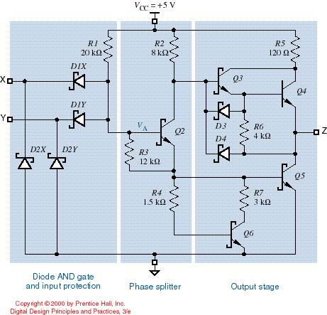
UNIT 2 BIPOLAR LOGIC AND INTERFACING BIPOLAR LOGIC FAMILIES
 UNIT 2 BIPOLAR LOGIC AND INTERFACING BIPOLAR LOGIC FAMILIES Bipolar logic families use semiconductor diodes and bipolar junction transistors as the basic building blocks of logic circuits The simplest
4-bit counter circa bit counter circa 1990
 Digital Logic 4-bit counter circa 1960 8-bit counter circa 1990 Logic gates Operates on logical values (TRUE = 1, FALSE = 0) NOT AND OR XOR 0-1 1-0 0 0 0 1 0 0 0 1 0 1 1 1 0 0 0 1 0 1 0 1 1 1 1 1 0 0 0
DIGITAL ELECTRONICS. Digital Electronics - B1 28/04/ DDC Storey 1. Group B: Digital circuits and devices
 Politecnico di Torino - ICT school Group B: Digital circuits and devices DIGITAL ELECTRONICS B DIGITAL CIRCUITS B.1 Logic devices B1 B2 B3 B4 Logic families Combinatorial circuits Basic sequential circuits
Lecture 02: Logic Families. R.J. Harris & D.G. Bailey
 Lecture 02: Logic Families R.J. Harris & D.G. Bailey Objectives Show how diodes can be used to form logic gates (Diode logic). Explain the need for introducing transistors in the output (DTL and TTL).
Chapter 6 Digital Circuit 6-6 Department of Mechanical Engineering
 MEMS1082 Chapter 6 Digital Circuit 6-6 TTL and CMOS ICs, TTL and CMOS output circuit When the upper transistor is forward biased and the bottom transistor is off, the output is high. The resistor, transistor,
Digital Integrated Circuits - Logic Families (Part II)
") Digital Integrated Circuits - Logic Families (Part II) MOSFET Logic Circuits MOSFETs are unipolar devices. They are simple, small in size, inexpensive to fabricate and consume less power. MOS fabrication
Digital Integrated Circuits - Logic Families (Part II) MOSFET Logic Circuits MOSFETs are unipolar devices. They are simple, small in size, inexpensive to fabricate and consume less power. MOS fabrication
DO NOT COPY DO NOT COPY
 184 hapter 3 Digital ircuits Table 3-13 Manufacturers logic data books. Manufacturer Order Number Topics Title Year Texas Instruments SDLD001 74, 74S, 74LS TTL TTL Logic Data Book 1988 Texas Instruments
Practice Homework Problems for Module 1
 Practice Homework Problems for Module 1 1. Unsigned base conversions (LO 1-1). (a) (2C9E) 16 to base 2 (b) (1101001) 2 to base 10 (c) (1101001) 2 to base 16 (d) (8576) 10 to base 16 (e) (A27F) 16 to base
IC Logic Families. Wen-Hung Liao, Ph.D. 5/16/2001
 IC Logic Families Wen-Hung Liao, Ph.D. 5/16/2001 Digital IC Terminology Voltage Parameters: V IH (min): high-level input voltage, the minimum voltage level required for a logic 1 at an input. V IL (max):
Digital Electronics Part II - Circuits
 Digital Electronics Part II - Circuits Dr. I. J. Wassell Gates from Transistors 1 Introduction Logic circuits are non-linear, consequently we will introduce a graphical technique for analysing such circuits
Basic Characteristics of Digital ICs
 ECEN202 Section 2 Characteristics of Digital IC s Part 1: Specification of characteristics An introductory look at digital IC s: Logic families Basic construction and operation Operating characteristics
Module-3: Metal Oxide Semiconductor (MOS) & Emitter coupled logic (ECL) families
 & Emitter coupled logic (ECL) families") 1 Module-3: Metal Oxide Semiconductor (MOS) & Emitter coupled logic (ECL) families 1. Introduction 2. Metal Oxide Semiconductor (MOS) logic 2.1. Enhancement and depletion mode 2.2. NMOS and PMOS inverter
1 Module-3: Metal Oxide Semiconductor (MOS) & Emitter coupled logic (ECL) families 1. Introduction 2. Metal Oxide Semiconductor (MOS) logic 2.1. Enhancement and depletion mode 2.2. NMOS and PMOS inverter
Chapter 6 DIFFERENT TYPES OF LOGIC GATES
 Chapter 6 DIFFERENT TYPES OF LOGIC GATES Lesson 9 CMOS gates Ch06L9-"Digital Principles and Design", Raj Kamal, Pearson Education, 2006 2 Outline CMOS (n-channel based MOSFETs based circuit) CMOS Features
36 Logic families and
 Unit 4 Outcomes 1. Demonstrate an understanding of logic families and their terms used in their specifications 2. Demonstrate an understanding of time division multiplex (TDM) 3. Demonstrate an understanding
Digital Electronics - B1 18/03/ /03/ DigElnB DDC. 18/03/ DigElnB DDC. 18/03/ DigElnB DDC
 Politecnico di Torino - ICT school Group B: Digital circuits and devices DIGITL ELECTRONICS B DIGITL CIRCUITS B.1 Logic devices B1 B2 B3 B4 Logic families Combinatorial circuits Basic sequential circuits
4-bit counter circa bit counter circa 1990
 Digital Logic 4-bit counter circa 1960 8-bit counter circa 1990 Logic gates Operates on logical values (TRUE = 1, FALSE = 0) NOT AND OR XOR 0-1 1-0 0 0 0 1 0 0 0 1 0 1 1 1 0 0 0 1 0 1 0 1 1 1 1 1 0 0 0
INTRODUCTION LOGIC SIGNALS AND GATES A logic value, 0 or 1, is often called a binary digit, or bit. If an application requires more than two discrete
 INTRODUCTION LOGIC SIGNALS AND GATES A logic value, 0 or 1, is often called a binary digit, or bit. If an application requires more than two discrete values, additional bits may be used, with a set of
Architecture of Computers and Parallel Systems Part 9: Digital Circuits
 Architecture of Computers and Parallel Systems Part 9: Digital Circuits Ing. Petr Olivka petr.olivka@vsb.cz Department of Computer Science FEI VSB-TUO Architecture of Computers and Parallel Systems Part
UNIT-I CMOS LOGIC. There are many, many ways to design an electronic logic circuit.
 UNIT-I CMOS LOGIC Introduction to Logic Families: There are many, many ways to design an electronic logic circuit. 1. The first electrically controlled logic circuits, developed at Bell Laboratories in
Digital Systems. CMOS Logic Structures. Sorin Hintea Departamentul de Bazele Electronicii
 Digital Systems CMOS Logic Structures Sorin Hintea Departamentul de Bazele Electronicii Outline CMOS logic structures CMOS technology CMOS inverter: structure, behavior, electrical parameters Noise margin;
Module-1: Logic Families Characteristics and Types. Table of Content
 1 Module-1: Logic Families Characteristics and Types Table of Content 1.1 Introduction 1.2 Logic families 1.3 Positive and Negative logic 1.4 Types of logic families 1.5 Characteristics of logic families
ECE 334: Electronic Circuits Lecture 10: Digital CMOS Circuits
 Faculty of Engineering ECE 334: Electronic Circuits Lecture 10: Digital CMOS Circuits CMOS Technology Complementary MOS, or CMOS, needs both PMOS and NMOS FET devices for their logic gates to be realized
Logic Families. A-PDF Split DEMO : Purchase from to remove the watermark. 5.1 Logic Families Significance and Types. 5.1.
 A-PDF Split DEMO : Purchase from www.a-pdf.com to remove the watermark 5 Logic Families Digital integrated circuits are produced using several different circuit configurations and production technologies.
LOGIC FAMILY LOGIC FAMILY
 In computer engineering, a logic family may refer to one of two related concepts. A logic family of monolithic digital integrated circuit devices is a group of electronic logic gates constructed using
ECE/CoE 0132: FETs and Gates
 ECE/CoE 0132: FETs and Gates Kartik Mohanram September 6, 2017 1 Physical properties of gates Over the next 2 lectures, we will discuss some of the physical characteristics of integrated circuits. We will
Logic Families. Describes Process used to implement devices Input and output structure of the device. Four general categories.
 Logic Families Characterizing Digital ICs Digital ICs characterized several ways Circuit Complexity Gives measure of number of transistors or gates Within single package Four general categories SSI - Small
Chapter 6 DIFFERENT TYPES OF LOGIC GATES
 Chapter 6 DIFFERENT TYPES OF LOGIC GATES Lesson 8 NMOS gates Ch06L8-"Digital Principles and Design", Raj Kamal, Pearson Education, 2006 2 Outline NMOS (n-channel based MOSFETs based circuit) NMOS Features
Transistor Digital Circuits
 Transistor Digital Circuits Switching Transistor Model (on) (on) T n T p Controlled switch model v CT > V CTex ; T- (on); i O > 0; v O 0 v CT < V Thn ; T- (off); i O = 0; v O = V PS v CT > V Thp ; T- (off);
Basic Logic Circuits
 Basic Logic Circuits Required knowledge Measurement of static characteristics of nonlinear circuits. Measurement of current consumption. Measurement of dynamic properties of electrical circuits. Definitions
DIGITAL ELECTRONICS. Digital Electronics - A2 28/04/ DDC Storey 1. Politecnico di Torino - ICT school. A2: logic circuits parameters
 Politecnico di Torino - ICT school A2: logic circuits parameters DIGITAL ELECTRONICS A INTRODUCTION A.2 Logic circuits parameters» Static parameters» Interfacing and compatibility» Output stages» Dynamic
LSN 3 Logic Gates. ECT 224 Digital Computer Fundamentals. Department of Engineering Technology
 LSN 3 Logic Gates Department of Engineering Technology LSN 3 Inverter One input and one output Produces a compliment of the input Negation indicator Truth table Active low output In Out 0 1 1 0 Active
DC Electrical Characteristics of MM74HC High-Speed CMOS Logic
 DC Electrical Characteristics of MM74HC High-Speed CMOS Logic The input and output characteristics of the MM74HC high-speed CMOS logic family were conceived to meet several basic goals. These goals are
EE 42/100 Lecture 23: CMOS Transistors and Logic Gates. Rev A 4/15/2012 (10:39 AM) Prof. Ali M. Niknejad
 Prof. Ali M. Niknejad") A. M. Niknejad University of California, Berkeley EE 100 / 42 Lecture 23 p. 1/16 EE 42/100 Lecture 23: CMOS Transistors and Logic Gates ELECTRONICS Rev A 4/15/2012 (10:39 AM) Prof. Ali M. Niknejad University
A. M. Niknejad University of California, Berkeley EE 100 / 42 Lecture 23 p. 1/16 EE 42/100 Lecture 23: CMOS Transistors and Logic Gates ELECTRONICS Rev A 4/15/2012 (10:39 AM) Prof. Ali M. Niknejad University
Chapter 15 Integrated Circuits
 Chapter 15 Integrated Circuits SKEE1223 Digital Electronics Mun im/arif/izam FKE, Universiti Teknologi Malaysia December 8, 2015 Overview 1 Basic IC Characteristics Packaging Logic Families Datasheets
ECE 301 Digital Electronics
 ECE 301 Digital Electronics Constraints in Logic Circuit Design (Lecture #14) The slides included herein were taken from the materials accompanying Fundamentals of Logic Design, 6 th Edition, by Roth and
Lecture Summary Module 1 Switching Algebra and CMOS Logic Gates
 Lecture Summary Module 1 Switching Algebra and CMOS Logic Gates Learning Outcome: an ability to analyze and design CMOS logic gates Learning Objectives: 1-1. convert numbers from one base (radix) to another:
ECE520 VLSI Design. Lecture 5: Basic CMOS Inverter. Payman Zarkesh-Ha
 ECE520 VLSI Design Lecture 5: Basic CMOS Inverter Payman Zarkesh-Ha Office: ECE Bldg. 230B Office hours: Wednesday 2:00-3:00PM or by appointment E-mail: pzarkesh@unm.edu Slide: 1 Review of Last Lecture
Propagation Delay, Circuit Timing & Adder Design. ECE 152A Winter 2012
 Propagation Delay, Circuit Timing & Adder Design ECE 152A Winter 2012 Reading Assignment Brown and Vranesic 2 Introduction to Logic Circuits 2.9 Introduction to CAD Tools 2.9.1 Design Entry 2.9.2 Synthesis
Propagation Delay, Circuit Timing & Adder Design
 Propagation Delay, Circuit Timing & Adder Design ECE 152A Winter 2012 Reading Assignment Brown and Vranesic 2 Introduction to Logic Circuits 2.9 Introduction to CAD Tools 2.9.1 Design Entry 2.9.2 Synthesis
DIGITAL ELECTRONICS. A2: logic circuits parameters. Politecnico di Torino - ICT school
 Politecnico di Torino - ICT school A2: logic circuits parameters DIGITAL ELECTRONICS A INTRODUCTION A.2 Logic circuits parameters» Static parameters» Interfacing and compatibility» Output stages» Dynamic
Design cycle for MEMS
 Design cycle for MEMS Design cycle for ICs IC Process Selection nmos CMOS BiCMOS ECL for logic for I/O and driver circuit for critical high speed parts of the system The Real Estate of a Wafer MOS Transistor
1 IC Logic Families and Characteristics
 2141 Electronics and Instrumentation IC1 1 IC Logic Families and Characteristics 1.1 Introduction miniature, low-cost electronics circuits whose components are fabricated on a single, continuous piece
EXPERIMENT 12: DIGITAL LOGIC CIRCUITS
 EXPERIMENT 12: DIGITAL LOGIC CIRCUITS The purpose of this experiment is to gain some experience in the use of digital logic circuits. These circuits are used extensively in computers and all types of electronic
Lab Project #2: Small-Scale Integration Logic Circuits
 Lab Project #2: Small-Scale Integration Logic Circuits Duration: 2 weeks Weeks of 1/31/05 2/7/05 1 Objectives The objectives of this laboratory project are to design some simple logic circuits using small-scale
In this experiment you will study the characteristics of a CMOS NAND gate.
 Introduction Be sure to print a copy of Experiment #12 and bring it with you to lab. There will not be any experiment copies available in the lab. Also bring graph paper (cm cm is best). Purpose In this
IC Logic Families and Characteristics. Dr. Mohammad Najim Abdullah
 IC Logic Families and Characteristics Introduction miniature, low-cost electronics circuits whose components are fabricated on a single, continuous piece of semiconductor material to perform a high-level
Unit-III. Digital integrated circuits
 Unit-III Digital integrated circuits Digital Integrated Circuits: Digital IC characteristics, Digital IC families -RTLand DTL, TL, I2L, TTL, ECL, MOS and CMOS logic circuits, Comparison of digital IC families
ECE 3160 DIGITAL SYSTEMS LABORATORY
 ECE 3160 DIGITAL SYSTEMS LABORATORY Experiment 2 Voltage and Current Characteristics of HC Device Electronics Reference: Wakerly chapter 3. Objectives: 1. To measure certain performance and voltage/current
Lecture 16. Complementary metal oxide semiconductor (CMOS) CMOS 1-1
 CMOS 1-1") Lecture 16 Complementary metal oxide semiconductor (CMOS) CMOS 1-1 Outline Complementary metal oxide semiconductor (CMOS) Inverting circuit Properties Operating points Propagation delay Power dissipation
Lecture 16 Complementary metal oxide semiconductor (CMOS) CMOS 1-1 Outline Complementary metal oxide semiconductor (CMOS) Inverting circuit Properties Operating points Propagation delay Power dissipation
Unit 1 Session - 3 TTL Parameters
 Objectives Understanding various TTL Parameters Floating Inputs Worst-Case Input Voltages & Output Voltages Profiles and Windows Compatibility Sourcing and Sinking Noise Immunity Standard Loading and Loading
INTEGRATED-CIRCUIT LOGIC FAMILIES
 C H A P T E R 8 INTEGRATED-CIRCUIT LOGIC FAMILIES OUTLINE 8-1 Digital IC Terminology 8-2 The TTL Logic Family 8-3 TTL Data Sheets 8-4 TTL Series Characteristics 8-5 TTL Loading and Fan-Out 8-6 Other TTL
ECE 471/571 The CMOS Inverter Lecture-6. Gurjeet Singh
 ECE 471/571 The CMOS Inverter Lecture-6 Gurjeet Singh NMOS-to-PMOS ratio,pmos are made β times larger than NMOS Sizing Inverters for Performance Conclusions: Intrinsic delay tp0 is independent of sizing
DELD UNIT 2. Question Option A Option B Option C Option D Correct Option. Current controlled. high input impedance and high output impedance
 Class : S.E.Comp Matoshri College of Engineering and Research Center Nasik Department of Computer Engineering Digital Elecronics and Logic Design (DELD) UNIT - II Subject : DELD Sr. No. 1 Transistor is
Introduction to Electronic Devices
 Introduction to Electronic Devices (Course Number 300331) Fall 2006 Dr. Dietmar Knipp Assistant Professor of Electrical Engineering Information: http://www.faculty.iubremen.de/dknipp/ Source: Apple Ref.:
Appendix B Page 1 54/74 FAMILIES OF COMPATIBLE TTL CIRCUITS PIN ASSIGNMENT (TOP VIEWS)
") Appendix B Page 1 54/74 FAMILIES OF COMPATIBLE TTL CIRCUITS PIN ASSIGNMENT (TOP VIEWS) See page 3 See page 3 See page 7 See page 14 See page 9 See page 16 See page 10 TEXAS INSTRUMENTS LTD have given their
Appendix B Page 1 54/74 FAMILIES OF COMPATIBLE TTL CIRCUITS PIN ASSIGNMENT (TOP VIEWS) See page 3 See page 3 See page 7 See page 14 See page 9 See page 16 See page 10 TEXAS INSTRUMENTS LTD have given their
High-Speed/Logic Gate Optocoupler (SFH67XX Series)
") Application Note High-Speed/Logic Gate Optocoupler (SFHXX Series) TRODUCTION The new SFHXX series of high-speed optocouplers is capable of transmitting data rates up to Mb/s typical and. Mb/s over the
Application Note High-Speed/Logic Gate Optocoupler (SFHXX Series) TRODUCTION The new SFHXX series of high-speed optocouplers is capable of transmitting data rates up to Mb/s typical and. Mb/s over the
Output Circuit of the TTL Gate
 JFETs, G a As DEVICES A N D CIRC UITS, A N D TTL CIRC UITS 27 28 MICR OELECTR ONIC CIRCUITS SEDRA /SMITH 14.3 TRANSISTOR TRANSISTOR LOGIC (TTL OR T 2 L) For more than two decades (late 1960s to late 1980s)
ELEC 350L Electronics I Laboratory Fall 2012
 ELEC 350L Electronics I Laboratory Fall 2012 Lab #9: NMOS and CMOS Inverter Circuits Introduction The inverter, or NOT gate, is the fundamental building block of most digital devices. The circuits used
Microelectronics, BSc course
 Microelectronics, BSc course MOS inverters http://www.eet.bme.hu/~poppe/miel/en/13-mosfet2.pptx http://www.eet.bme.hu Overview of MSOFET types 13-11-2014 Microelectronics BSc course, MOS inverters András
CMOS the Ideal Logic Family
 CMOS the Ideal Logic Family National Semiconductor Application Note 77 Stephen Calebotta January 1983 INTRODUCTION Let s talk about the characteristics of an ideal logic family It should dissipate no power
1. Draw the circuit diagram of basic CMOS gate and explain the operation. VOUT=VDD
 1. Draw the circuit diagram of basic CMOS gate and explain the operation. The basic CMOS inverter circuit is shown in below figure. It consists of two MOS transistors connected in series (1-PMOS and 1-NMOS).
Note that none of the above MAY be a VALID ANSWER.
 ECE 270 Learning Outcome 1-1 - Practice Exam / Solution LEARNING OUTCOME #1: an ability to analyze and design CMOS logic gates. Multiple Choice select the single most appropriate response for each question.
Digital Integrated CircuitDesign
 Digital Integrated CircuitDesign Lecture 11 BiCMOS PMOS rray Q1 NMOS rray Y NMOS rray Q2 dib brishamifar EE Department IUST Contents Introduction BiCMOS Devices BiCMOS Inverters BiCMOS Gates BiCMOS Drivers
APPENDIX C IC INTERFACING AND SYSTEM DESIGN ISSUES
 APPENDIX C IC INTERFACING AND SYSTEM DESIGN ISSUES OVERVIEW This appendix provides an overview of IC technology and AVR interfacing. In addition, we look at the microcontroller-based system as a whole
Lecture 13 - Digital Circuits (II) MOS Inverter Circuits. October 25, 2005
 MOS Inverter Circuits. October 25, 2005") 6.12 - Microelectronic Devices and Circuits - Fall 25 Lecture 13-1 Lecture 13 - Digital Circuits (II) MOS Inverter Circuits October 25, 25 Contents: 1. NMOS inverter with resistor pull-up (cont.) 2. NMOS
6.12 - Microelectronic Devices and Circuits - Fall 25 Lecture 13-1 Lecture 13 - Digital Circuits (II) MOS Inverter Circuits October 25, 25 Contents: 1. NMOS inverter with resistor pull-up (cont.) 2. NMOS
CD54/74HC139, CD54/74HCT139
 Data sheet acquired from Harris Semiconductor SCHS148B September 1997 - Revised May 2000 CD54/74HC139, CD54/74HCT139 High-Speed CMOS Logic Dual 2-to-4 Line Decoder/Demultiplexer [ /Title (CD74 HC139, CD74
DIGITAL LOGIC CIRCUITS
 EE6301 DIGITAL LOGIC CIRCUITS LT P C 3 1 0 4 OBJECTIVES: To study various number systems, simplify the logical expressions using Boolean functions To study implementation of combinational circuits To design
FAMILIARIZATION WITH DIGITAL PULSE AND MEASUREMENTS OF THE TRANSIENT TIMES
 EXPERIMENT 1 FAMILIARIZATION WITH DIGITAL PULSE AND MEASUREMENTS OF THE TRANSIENT TIMES REFERENCES Analysis and Design of Digital Integrated Circuits, Hodges and Jackson, pages 6-7 Experiments in Microprocessors
BICMOS Technology and Fabrication
 12-1 BICMOS Technology and Fabrication 12-2 Combines Bipolar and CMOS transistors in a single integrated circuit By retaining benefits of bipolar and CMOS, BiCMOS is able to achieve VLSI circuits with
Module 4 : Propagation Delays in MOS Lecture 19 : Analyzing Delay for various Logic Circuits
 Module 4 : Propagation Delays in MOS Lecture 19 : Analyzing Delay for various Logic Circuits Objectives In this lecture you will learn the following Ratioed Logic Pass Transistor Logic Dynamic Logic Circuits
Logic families (TTL, CMOS)
") Logic families (TTL, CMOS) When you work with digital IC's, you should be familiar, not only with their logical operation, but also with such operational properties as voltage levels, noise immunity, power
Logic families (TTL, CMOS) When you work with digital IC's, you should be familiar, not only with their logical operation, but also with such operational properties as voltage levels, noise immunity, power
TC74AC05P,TC74AC05F,TC74AC05FN
 TOSHIBA CMOS Digital Integrated Circuit Silicon Monolithic TC74AC05P/F/FN TC74AC05P,TC74AC05F,TC74AC05FN Hex Inverter (open drain) The TC74AC05 is an advanced high speed CMOS INVERTER fabricated with silicon
Code No: R Set No. 1
 Code No: R05310402 Set No. 1 1. (a) What are the parameters that are necessary to define the electrical characteristics of CMOS circuits? Mention the typical values of a CMOS NAND gate. (b) Design a CMOS
CD54HC273, CD74HC273, CD54HCT273, CD74HCT273
 Data sheet acquired from Harris Semiconductor SCHS174B February 1998 - Revised May 2003 CD54HC273, CD74HC273, CD54HCT273, CD74HCT273 High-Speed CMOS Logic Octal D-Type Flip-Flop with Reset [ /Title (CD74
Department of EECS. University of California, Berkeley. Logic gates. September 1 st 2001
 Department of EECS University of California, Berkeley Logic gates Bharathwaj Muthuswamy and W. G. Oldham September 1 st 2001 1. Introduction This lab introduces digital logic. You use commercially available
. HIGH SPEED .LOW POWER DISSIPATION .COMPATIBLE WITH TTL OUTPUTS M54/74HCT245/640/643 M54/74HCT245/640/643
 M54/74HCT245/640/643 M54/74HCT245/640/643 OCTAL BUS TRANSCEIVER (3-STATE): HCT245 NON INVERTING HCT640 INVERTING, HCT643 INVERTING/NON INVERTING. HIGH SPEED t PD = 10 ns (TYP.) at V CC =5V.LOW POWER DISSIPATION
ECE380 Digital Logic. Logic values as voltage levels
 ECE380 Digital Logic Implementation Technology: NMOS and PMOS Transistors, CMOS logic gates Dr. D. J. Jackson Lecture 13-1 Logic values as voltage levels V ss is the minimum voltage that can exist in the
UNISONIC TECHNOLOGIES CO., LTD CD4069
 UNISONIC TECHNOLOGIES CO., LTD CD4069 INVERTER CIRCUITS DESCRIPTION The UTC CD4069 consists of six inverter circuits and is manufactured using complementary MOS (CMOS) to achieve wide power supply operating
UNIT IV. Logic families can be classified broadly according to the technologies they are built with. The various technologies are listed below.
 UNIT IV Digital Logic Families Logic families can be classified broadly according to the technologies they are built with. The various technologies are listed below. DL : Diode Logic. RTL : Resistor Transistor
EEC 118 Lecture #11: CMOS Design Guidelines Alternative Static Logic Families
 EEC 118 Lecture #11: CMOS Design Guidelines Alternative Static Logic Families Rajeevan Amirtharajah University of California, Davis Jeff Parkhurst Intel Corporation Announcements Homework 5 this week Lab
Electronic Circuits EE359A
 Electronic Circuits EE359A Bruce McNair B206 bmcnair@stevens.edu 201-216-5549 1 Memory and Advanced Digital Circuits - 2 Chapter 11 2 Figure 11.1 (a) Basic latch. (b) The latch with the feedback loop opened.
OCTAL BUFFER/LINE DRIVER WITH 3-STATE OUTPUTS
 P54FCT241T/74fct241t OCTAL BUFFER/LINE DRIVER WITH 3-STATE OUTPUTS FEATURES Function, Pinout and Drive Compatible with the FCT and F Logic FCT-A speed at 5.1ns max (MIL) Reduced VOH (typically = 3.3V)
MM74HC132 Quad 2-Input NAND Schmitt Trigger
 Quad 2-Input NAND Schmitt Trigger General Description The utilizes advanced silicon-gate CMOS technology to achieve the low power dissipation and high noise immunity of standard CMOS, as well as the capability
CPE/EE 427, CPE 527 VLSI Design I CMOS Inverter. CMOS Inverter: A First Look
 CPE/EE 427, CPE 527 VLSI Design I CMOS Inverter Department of Electrical and Computer Engineering University of Alabama in Huntsville Aleksandar Milenkovic CMOS Inverter: A First Look C L 9/11/26 VLSI
MM74HCU04 Hex Inverter
 MM74HCU04 Hex Inverter General Description The MM74HCU04 inverters utilize advanced silicon-gate CMOS technology to achieve operating speeds similar to LS-TTL gates with the low power consumption of standard
P54FCT240T/74fct240T FEATURES DESCRIPTION. Function, Pinout and Drive Compatible with the FCT and F Logic. ESD protection exceeds 2000V
 P54FCT240T/74fct240T inverting OCTAL BUFFER/LINE DRIVER WITH 3-STATE OUTPUTS FEATURES Function, Pinout and Drive Compatible with the FCT and F Logic FCT-A speed at 5.1ns max (MIL) Reduced VOH (typically
INTEGRATED CIRCUITS. AN243 LVT (Low Voltage Technology) and ALVT (Advanced LVT)
 and ALVT (Advanced LVT)") INTEGRATED CIRCUITS LVT (Low Voltage Technology) and ALVT (Advanced LVT) Author: Tinus van de Wouw January 1998 Author: Tinus van de Wouw, Philips Semiconductors, Nijmegen 1 INTRODUCTION Philips Semiconductors
INTEGRATED CIRCUITS LVT (Low Voltage Technology) and ALVT (Advanced LVT) Author: Tinus van de Wouw January 1998 Author: Tinus van de Wouw, Philips Semiconductors, Nijmegen 1 INTRODUCTION Philips Semiconductors
Digital Systems Laboratory
 2012 Fall CSE140L Digital Systems Laboratory Lecture #2 by Dr. Choon Kim CSE Department, UCSD chk034@eng.ucsd.edu Lecture #2 1 Digital Technologies CPU(Central Processing Unit) GPU(Graphics Processing
. HIGH SPEED .LOW POWER DISSIPATION .COMPATIBLE WITH TTL OUTPUTS M54/74HCT373 M54/74HCT533
 M54/74HCT373 M54/74HCT533 OCTAL D-TYPE LATCH WITH 3 STATE OUTPUT HCT373 NON INVERTING - HCT533 INVERTING. HIGH SPEED t PD = 17 ns (TYP.) AT V CC =5V.LOW POWER DISSIPATION ICC =4µA (MAX.) AT TA =25 C.COMPATIBLE
MOS TRANSISTOR THEORY
 MOS TRANSISTOR THEORY Introduction A MOS transistor is a majority-carrier device, in which the current in a conducting channel between the source and the drain is modulated by a voltage applied to the
Chapter 7 EMITTER-COUPLED LOGIC
 Chapter 7 EMITTER-COUPLED LOGIC The major speed limitation of TTL is the turn-off time of saturated transistors. To be sure, TTL has come a long way from the 100 ns time of DTL to the 2-4 ns propagation
Schmitt Trigger Inputs, Decoders
 Schmitt Trigger, Decoders Page 1 Schmitt Trigger Inputs, Decoders TTL Switching In this lab we study the switching of TTL devices. To do that we begin with a source that is unusual for logic circuits,
In data sheets and application notes which still contain NXP or Philips Semiconductors references, use the references to Nexperia, as shown below.
 Important notice Dear Customer, On 7 February 2017 the former NXP Standard Product business became a new company with the tradename Nexperia. Nexperia is an industry leading supplier of Discrete, Logic