BEC402-ELECTRONIC CIRCUITS
|
|
|
- Grace Hart
- 6 years ago
- Views:
Transcription
1 BEC402-ELECTRONIC CIRCUITS
2 UNIT- I BASIC DEVICE STABILIZATION AND LOW FREQUENCY DESIGN ANALYSIS Circuits for BJT, DC and AC Load lines, Stability factor analysis, Temperature compensation methods, biasing circuits for FET's and MOSFET's. Transistor, FET and MOSFET Amplifiers, Equivalent circuit, input and output characteristics, calculation of midband gain, input and output impedance of various amplifiers, cascode amplifier, Darlington Bootstrapping. Differential amplifier, CMRR measurement, Use of current source in Emitter.
3 INTRODUCTION The BJT as a circuit element operates various circuits with many major and minor modifications. For the analysis of such circuits, we obtain the various conditions for proper operation of the device, and also determine the projected range of operation of the device.
4 A detailed study of the device in a two-port mode simplifies the circuit analysis of the device to a large extent. Thus, we calculate the various parameters of the devices performance, namely voltage gain, current gain, input impedance, and output impedance. The frequency response of the device is dealt with in detail, and a study of the various regions of operation in the frequency scale is also explained. Finally, we will discuss the various configurations of the device and take a look into the high-frequency operation of the device and its performance in those regions.
5 Proper Transistor Biasing For a transistor to function properly as an amplifier, the emitter-base junction must be forward-biased and the collector-base junction must be reverse-biased. The common connection for the voltage sources are at the base lead of the transistor. The emitter-base supply voltage is designated V EE and the collector-base supply voltage is designated V CC. For silicon, the barrier potential for both EB and CB junctions equals 0.7 V
6 Transistor Biasing The basic function of transistor is amplification. The process of raising the strength of weak signal without any change in its general shape is referred as faithful amplification. For faithful amplification it is essential that:- 1. Emitter-Base junction is forward biased 2. Collector- Base junction is reversed biased 3. Proper zero signal collector current The proper flow of zero signal collector current and the maintenance of proper collector emitter voltage during the passage of signal is called transistor biasing. 6
7 Why Biasing? If the transistor is not biased properly, it would work inefficiently and produce distortion in output signal. How A Transistor Can Be Biased? A transistor is biased either with the help of battery or associating a circuit with the transistor. The later method is more efficient and is frequently used. The circuit used for transistor biasing is called the biasing circuit. 7
8 BIAS STABILITY Through proper biasing, a desired quiescent operating point of the transistor amplifier in the active region (linear region) of the characteristics is obtained. It is desired that once selected the operating point should remain stable. The maintenance of operating point stable is called Stabilisation. 8
9 The selection of a proper quiescent point generally depends on the following factors: (a)the amplitude of the signal to be handled by the amplifier and distortion level in signal (b)the load to which the amplifier is to work for a corresponding supply voltage The operating point of a transistor amplifier shifts mainly with changes in temperature, since the transistor parameters β, I CO and V BE (where the symbols carry their usual meaning) are functions of temperature.
10 The DC Operating Point For a transistor circuit to amplify it must be properly biased with dc voltages. The dc operating point between saturation and cutoff is called the Q-point. The goal is to set the Q-point such that that it does not go into saturation or cutoff when an a ac signal is applied. 10
11 The Thermal Stability of Operating Point (S Ico) Stability Factor S:- The stability factor S, as the change of collector current with respect to the reverse saturation current, keeping β and VBE constant. This can be written as: The Thermal Stability Factor : S Ico S Ico = I c I co V be, β 11
12 This equation signifies that I c Changes S Ico times as fast as I co Differentiating the equation of Collector Current I C = (1+β)Ico+ βib & rearranging the terms we can write S Ico 1+β و 1- β ( I b / I C ) It may be noted that Lower is the value of S Ico better is the stability
13 Various Biasing Circuits Fixed Bias Circuit Fixed Bias with Emitter Resistor Collector to Base Bias Circuit Potential Divider Bias Circuit 13
14 The Fixed Bias Circuit The Thermal Stability Factor : S Ico 15 V 15 V 200 k R C 1 k R b S Ico = I c I co V be, β C R C I b B E General Equation of S Ico Comes out to S Ico 1 + β 1- β ( I b / I C ) 14
15 Applying KVL through Base Circuit we can write, I b R b + V be = V cc Diff w. r. t. I C, we get ( I b / I c ) = 0 S Ico = (1+β) is very large Indicating high unstability
16 Merits: It is simple to shift the operating point anywhere in the active region by merely changing the base resistor (RB). A very small number of components are required. Demerits: The collector current does not remain constant with variation in temperature or power supply voltage. Therefore the operating point is unstable. 16
17 When the transistor is replaced with another one, considerable change in the value of β can be expected. Due to this change the operating point will shift. For small-signal transistors (e.g., not power transistors) with relatively high values of β (i.e., between 100 and 200), this configuration will be prone to thermal runaway. In particular, the stability factor, which is a measure of the change in collector current with changes in reverse saturation current, is approximately β+1. To ensure absolute stability of the amplifier, a stability factor of less than 25 is preferred, and so small-signal transistors have large stability factors.
18 Fixed bias with emitter resistor The fixed bias circuit is modified by attaching an external resistor to the emitter. This resistor introduces negative feedback that stabilizes the Q-point. 18
19 Merits: The circuit has the tendency to stabilize operating point against changes in temperature and β-value. Demerits: As β-value is fixed for a given transistor, this relation can be satisfied either by keeping RE very large, or making RB very low. 19
20 The Collector to Base Bias Circuit R F I b + B V BE V CC R C I c C E - I E This configuration employs negative feedback to prevent thermal runaway and stabilize the operating point. In this form of biasing, the base resistor RF is connected to the collector instead of connecting it to the DC source Vcc. So any thermal runaway will induce a voltage drop across the Rc resistor that will throttle the transistor's base current. 20
21 Applying KVL through base circuit we can write (I b + I C ) R C + I b R f + V be = V cc Diff. w. r. t. I C we get ( I b / I c ) = - R C / (R f + R C ) Therefore, S Ico (1+ β) 1+ [βr C /(R C + R f )] Which is less than (1+β), signifying better thermal stability 21
22 Merits: Circuit stabilizes the operating point against variations in temperature and β (i.e. replacement of transistor) Demerits: As β -value is fixed (and generally unknown) for a given transistor, this relation can be satisfied either by keeping Rc fairly large or making Rf very low. Usage: The feedback also decreases the input impedance of the amplifier as seen from the base, which can be advantageous. Due to the gain reduction from feedback, this biasing form is used only when the trade-off for stability is warranted. 22
23 The Potential Divider Bias Circuit This is the most commonly used arrangement for biasing as it provide good bias stability. In this arrangement the emitter resistance RE provides stabilization. The resistance RE cause a voltage drop in a direction so as to reverse bias the emitter junction. Since the emitter-base junction is to be forward biased, the base voltage is obtained from R1- R2 network. 23
24 The Potential Divider Bias Circuit The net forward bias across the emitter base junction is equal to VB- dc voltage drop across RE RE. The base voltage is set by Vcc and R1 and R2. The dc bias circuit is independent of transistor current gain. In case of amplifier, to avoid the loss of ac signal, a capacitor of large capacitance is connected across RE. The capacitor offers a very small reactance to ac signal and so it passes through the condensor.
25 The Potential Divider Bias Circuit V CC R 1 I b B I C V CC R C C To find the stability of this circuit we have to convert this circuit into its Thevenin s Equivalent circuit R 2 I E E R E R th = R 1 *R 2 & V th = Vcc R 2 th = R 1 *R 2 & V th = Vcc R 2 R 1 +R 2 R 1 +R 2 25
26 The Potential Divider Bias Circuit + _ Thevenin Equivalent Ckt I b R Th V Th Thevenin Equivalent Voltage I C B IE V CC C E R C R E Self-bias Resistor Applying KVL through input base circuit we can write I b R Th + I E R E + V be = V Th Therefore, I b R Th + (I C + I b ) R E + V BE = V Th Diff. w. r. t. I C & rearranging we get ( I b / I c ) = - R E / (R Th + R E ) Therefore, 1 SIco RE 1 R E RTh
27 Merits: Operating point is almost independent of β variation. Operating point stabilized against shift in temperature. Demerits: As β-value is fixed for a given transistor, this relation can be satisfied either by keeping RE fairly large, or making R1 R2 very low. 27
28 If RE is of large value, high VCC is necessary. This increases cost as well as precautions necessary while handling. AC as well as DC feedback is caused by RE, which reduces the AC voltage gain of the amplifier. A method to avoid AC feedback while retaining DC feedback is discussed below.
29 Usage: The circuit's stability and merits as above make it widely used for linear circuits. If R1 R2 is low, either R1 is low, or R2 is low, or both are low. A low R1 raises VB closer to VC, reducing the available swing in collector voltage, and limiting how large RC can be made without driving the transistor out of active mode. A low R2 lowers Vbe, reducing the allowed collector current. Lowering both resistor values draws more current from the power supply and lowers the input resistance of the amplifier as seen from the base.
30 Biasing And Bias Stability Biasing refers to the establishment of suitable dc values of different currents and voltages of a transistor. Through proper biasing, a desired quiescent operating point of the transistor amplifier in the active region (linear region) of the characteristics is obtained. The selection of a proper quiescent point generally depends on the following factors: (a)the amplitude of the signal to be handled by the amplifier and distortion level in signal (b)the load to which the amplifier is to work for a corresponding supply voltage
31 The operating point of a transistor amplifier shifts mainly with changes in temperature, since the transistor parameters β, I CO and V BE (where the symbols carry their usual meaning) are functions of temperature. Circuit Configurations Fixed-bias circuit Fixed bias with emitter resistance Voltage-divider bias Voltage-feedback biasing
32 Biasing And Bias Stability Fixed-bias circuit Base emitter loop Collector emitter loop and (a) Representation of fixed-bias circuit (b) Equivalent circuit
33 Biasing And Bias Stability Fixed bias with emitter resistance Base emitter loop and the emitter current can be written as From above two equation we get: Collector emitter loop
34 with the base current known, I C calculated by the relation I C = βi B. can be easily Fixed-bias circuit with emitter resistance
35 Biasing And Bias Stability Voltage-divider bias:- The Thevenins equivalent voltage and resistance for the input side is given by: The KVL equation for the input circuit is given as: Voltage-divider bias circuit Simplified voltage-divider circuit
36 Biasing And Bias Stability Voltage-feedback biasing Base emitter loop Applying KVL for this part, we get: Thus, the base current can be obtained as: Representation of Voltage-feedback biased circuit
37 Biasing And Bias Stability Stabilization Against Variations in ICO, VBE, and β Transfer characteristic:- In this particular characteristic, the output current IC is a function of input voltage for the germanium transistor. Thus, the word transfer is used for this characteristic. Transfer characteristics for germanium p n p alloy type transistor
38 Biasing And Bias Stability Self-bias circuit Collector current vs. base-to-emitter voltage for a silicon transistor
39 Biasing And Bias Stability Variation of the collector current with temperature because of VBE, ICO and β
40 Transistor Biasing For a transistor to function properly as an amplifier, an external dc supply voltage must be applied to produce the desired collector current. Bias is defined as a control voltage or current. Transistors must be biased correctly to produce the desired circuit voltages and currents. The most common techniques used in biasing are Base bias Voltage-divider bias Emitter bias
41 Fig. -1 (a) shows the simplest way to bias a transistor, called base bias. V BB is the base supply voltage, which is used to forward-bias the base-emitter junction. R B is used to provide the desired value of base current. V CC is the collector supply voltage, which provides the reverse-bias voltage required for the collector-base junction. The collector resistor, R C, provides the desired voltage in the collector circuit Transistor Biasing Fig. -1
42 Transistor Biasing: Base Biasing A more practical way to provide base bias is to use one power supply. I B = V CC - V BE R B I C dc x I B V CE V CC - I C R C
43 Transistor Biasing The DC load line is a graph that allows us to determine all possible combinations of I C and V CE for a given amplifier. For every value of collector current, I C, the corresponding value of V CE can be found by examining the dc load line. A sample dc load line is shown in Fig. 1. Fig. 1
44 Transistor Biasing Midpoint Bias Without an ac signal applied to a transistor, specific values of I C and V CE exist at a specific point on a dc load line This specific point is called the Q point (quiescent currents and voltages with no ac input signal) An amplifier is biased such that the Q point is near the center of dc load line I CQ = ½ I C(sat) V CEQ = ½ V CC Base bias provides a very unstable Q point, because I C and V CE are greatly affected by any change in the transistor s beta value
45 Fig. 2 illustrates a dc load line showing the end points I C (sat) and V CE (off), as well as the Q point values I CQ and V CEQ. Transistor Biasing Fig. 2
46 Transistor Biasing The most popular way to bias a transistor is with voltage-divider bias. The advantage of voltage-divider bias lies in its stability. An example of voltage-divider bias is shown in Fig V B = R 2 R 1 + R 2 X V CC V E = V B - V BE Fig I E I C
47 Voltage Divider Bias Example Solve for V B, V E, I E, I C, V C and V CE Construct a dc load line showing the values of I C(sat), V CE(off), I CQ and V CEQ
48 Transistor Biasing Fig shows the dc load line for voltage-divider biased transistor circuit in Fig End points and Q points are I C (sat) = ma V CE (off) = 15 V I CQ = 7 ma V CEQ = 6.32 V Fig
49 Calculation Of Stability Factors Stability Factor S:- The stability factor S, as the change of collector current with respect to the reverse saturation current, keeping β and V BE constant. This can be written as: Or, Stability Factor S :- The variation of I C with V BE is given by the stability factor S defined by the partial derivative:
50 Stability Factor S :- The variation of I C with respect to β is represented by the stability factor, S'', given as: General Remarks on Collector Current Stability:- The stability factors have been defined earlier keeping in mind the change in collector current with respect to changes in I CO, V BE and β. These stability factors are repeated here for simplicity.
51 Thermal Runaway The maximum average power in which a transistor can dissipate depends upon the construction of transistor and lie in the range of few milliwatts and 200W. The maximum power is limited by the temperature that the collector Base junction can withstand. The maximum power dissipation is usually specified for the transistor enclosure is 25 degree celsius. The junction temperature may increase either because of rise in ambient temperature or because of self heating. The problem of self heating arises due to dissipation of power at the collector junction.
52 The leakage current Icbo is extremely temperature dependent and increases with the rise in temperature of collector-base junction. With the increase in collector current Ic, collector power dissipation increases which raises the junction temperature that leads to further increase in collector current Ic. The process is cumulative and may lead to the eventual destruction of transistor. This phenomenon is known as THERMAL RUNAWAY of transistor. In practice the Thermal Runaway can be prevented by a well designed circuit called as STABILIZATION Circuitry.
53 Diode Compensation Techniques Compensation for V BE : Diagram shows the voltage divider bias with bias compensation technique.here, separate supply V DD is used to keep diode in forward If biased condition. If the diode used in the circuit is of same material and type as the transistor, the voltage across the diode will have the same temperature coefficient as the base to emitter voltage V BE. So when V BE changes by V BE with change in temperature, V D changes by V D and V D~ =~ V BE, the changes tend to cancel each other. Apply*g KVL to the base circuit of Fig.,we have
54
55
56 Diode is connected in series with resistance R 2 in the voltage divider circuit and it is forward biased condition. For voltage divider bias, When V BE changes with temperature, I C also changes To cancel the changes in I C, one diode is used in the circuit for compensation
57 Compensation for I CO * In germanium transistor changes in I CO with temperature plays an important role collector current stability * The diode is kept at reverse bias condition,so only leakage current flows * I o increases then I CO also increases
58
59 Thermistor Compensation
60 Fig (b) shows another thermistor compensation technique. Here, thermistor is connected between emitter and Vcc to minimize the increase in collector current due to changes in ICO, VBE, or beta with temperature.i C increases with temperature and R T decreases with increase in temperature. Therefore, current flowing through RE increases, which increases the voltage drop across it. E - B junction is forward biased. But due to increase in voltage drop across R E, emitter is made more positive, which reduces the forward bias voltage V BE. Hence, bias current reduces. As Ico increases with temperature, I B hence. IC remains constant decreases and
61 Sensistor Compensation technique
62 This method of transistor compensation uses temperature sensitive resistive element, sensistors rather than diodes or transistors. It has a positive temperature coefficient, its resistance increases exponentially with increasing temperature as shown in the Fig Slope of this curve = is the temperature coefficient for thermistor and the slope is positive So we can say that sensistor has positive temperature coefficient of resistance (PTC).
63 Biasing Circuits used for JFET Fixed bias circuit Self bias circuit Potential Divider bias circuit
64 JFET (n-channel) Biasing Circuits For Fixed Bias Circuit Applying KVL to gate circuit we get I DS I DSS V 1 V GS P 2 V GG and I I DS and G R V G I DS V DSS GS 1 V V DD V V GS GS P I Fixed, I 0 DS 2 R D G Where, V p =V GS-off & I DSS is Short ckt. I DS For Self Bias Circuit V GS I DS I R 0 DS V S R GS S
65 or Fixed Bias Ckt. JFET Biasing Circuits Contd
66 JFET Self (or Source) Bias Circuit 2 1 and P GS DSS DS V V I I S GS P GS DSS R V V V I S GS P GS P GS DSS R V V V V V I This quadratic equation can be solved for V GS & I DS
67 The Potential (Voltage) Divider Bias I DSS 1 V V GS P 2 V G R V S GS 0 Solving this quadratic equation gives V GS and I DS
68 DC analysis step for Feedback Biasing Enhancement type MOSFET Find k using the datasheet or specification given; ex: V GS(ON),V GS(TH) Plot transfer characteristics using the formula I D =k(v GS V T ) 2. Three point already defined that is I D(ON), V GS(ON) and V GS(TH) Plot a point that is slightly greater than V GS Plot the linear characteristics (network bias line) The intersection defines the Q-point 68
69 Voltage-Divider Biasing Again plot the line and the transfer curve to find the Q-point. 2 DD Using the following equations: R V Input loop : Output loop : V V GS DS V V G DD I D I R D S V G ( R RD ) S R 1 R 2 69
70 UNIT II LARGE SIGNAL AMPLIFIERS Class A, AB, B, C and D type of operation, efficiency of Class A amplifier with resistive and transformer coupled load, efficiency of Class B, Complementry Symmetry amplifiers, MOSFET Power amplifiers, Thermal stability of Power amplifiers, heat sink design
71 Classes of Amplifiers Introduction One method used to distinguish the electrical characteristics of different types of amplifiers is by class, and as such amplifiers are classified according to their circuit configuration and method of operation. Then Amplifier Classes is the term used to differentiate between the different amplifier types.
72 Amplifier Classes represent the amount of the output signal which varies within the amplifier circuit over one cycle of operation when excited by a sinusoidal input signal. The classification of amplifiers range from entirely linear operation (for use in high-fidelity signal amplification) with very low efficiency, to entirely non-linear (where a faithful signal reproduction is not so important) operation but with a much higher efficiency, while others are a compromise between the two.
73 Amplifier classes are mainly lumped into two basic groups. The first are the classically controlled conduction angle amplifiers forming the more common amplifier classes of A, B, AB and C, which are defined by the length of their conduction state over some portion of the output waveform, such that the output stage transistor operation lies somewhere between being fully-on and fully-off.
74 The second set of amplifiers are the newer socalled switching amplifier classes of D, E, F, G, S, T etc, which use digital circuits and pulse width modulation (PWM) to constantly switch the signal between fully-on and fully-off driving the output hard into the transistors saturation and cut-off regions.
75 Class A Amplifier
76 To achieve high linearity and gain, the output stage of a class A amplifier is biased ON (conducting) all the time. Then for an amplifier to be classified as Class A the zero signal idle current in the output stage must be equal to or greater than the maximum load current (usually a loudspeaker) required to produce the largest output signal. As a class A amplifier operates in the linear portion of its characteristic curves, the single output device conducts through a full 360 degrees of the output waveform. Then the class A amplifier is equivalent to a current source.
77 Class B Amplifier Class B amplifiers were invented as a solution to the efficiency and heating problems associated with the previous class A amplifier. The basic class B amplifier uses two complimentary transistors either bipolar of FET for each half of the waveform with its output stage configured in a push-pull type arrangement, so that each transistor device amplifies only half of the output waveform.
78 Class B Amplifier
79 When the input signal goes positive, the positive biased transistor conducts while the negative transistor is switched OFF. Likewise, when the input signal goes negative, the positive transistor switches OFF while the negative biased transistor turns ON and conducts the negative portion of the signal. Thus the transistor conducts only half of the time, either on positive or negative half cycle of the input signal. Then we can see that each transistor device of the class B amplifier only conducts through one half or 180 degrees of the output waveform in strict time alternation, but as the output stage has devices for both halves of the signal waveform the two halves are combined together to produce the full linear output waveform.
80 Class AB Amplifier As its name suggests, the Class AB Amplifier is a combination of the Class A and the Class B type amplifiers we have looked at above. The AB classification of amplifier is currently one of the most common used types of audio power amplifier design. The class AB amplifier is a variation of a class B amplifier as described above, except that both devices are allowed to conduct at the same time around the waveforms crossover point eliminating the crossover distortion problems of the previous class B amplifier.
81 Class AB Amplifier
82 The advantage of this small bias voltage, provided by series diodes or resistors, is that the crossover distortion created by the class B amplifier characteristics is overcome, without the inefficiencies of the class A amplifier design. So the class AB amplifier is a good compromise between class A and class B in terms of efficiency and linearity, with conversion efficiencies reaching about 50% to 60%.
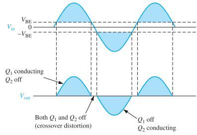
83 Class C Amplifier The Class C Amplifier design has the greatest efficiency but the poorest linearity of the classes of amplifiers mentioned here. The previous classes, A, B and AB are considered linear amplifiers, as the output signals amplitude and phase are linearly related to the input signals amplitude and phase. However, the class C amplifier is heavily biased so that the output current is zero for more than one half of an input sinusoidal signal cycle with the transistor idling at its cut-off point.
84 Class C Amplifier
85 Due to its heavy audio distortion, class C amplifiers are commonly used in high frequency sine wave oscillators and certain types of radio frequency amplifiers, where the pulses of current produced at the amplifiers output can be converted to complete sine waves of a particular frequency by the use of LC resonant circuits in its collector circuit.
86 Class D Power Amplifier
87 A Class D audio amplifier is basically a non-linear switching amplifier or PWM amplifier. Class-D amplifiers theoretically can reach 100% efficiency, as there is no period during a cycle were the voltage and current waveforms overlap as current is drawn only through the transistor that is on.
88 Amplifier Classes and Efficiency
89 Amplifier Class by Conduction Angle Amplifier Class Class-A Class-B Class-AB Class-C Class-D to T Description Full cycle 360 o of Conduction Half cycle 180 o of Conduction Slightly more than 180 o of conduction Slightly less than 180 o of conduction ON-OFF non-linear switching Conduction Angle θ = 2π θ = π π < θ < 2π θ < π θ = 0
90 Crossover Distortion When the dc base voltage is zero, both transistors are off and the input signal voltage must exceed VBE before a transistor conducts. Because of this, there is a time interval between the positive and negative alternations of the input when neither transistor is conducting, as shown in Figure. The resulting distortion in the output waveform is called crossover distortion.
91
92 Thermal stability of Power amplifiers Each heat-sink has a parameter called its Thermal Resistance (Rth) measured in C/Watt and the lower the value of Rth the faster heat is dissipated. Other factors affecting heat dissipation include the power (in Watts) being dissipated by the transistor, the efficiency of heat transfer between the internal transistor junction and the transistor case, and the case to the heat-sink. The difference between the temperature of the heatsink and the air temperature surrounding the heat-sink (the ambient temperature) must also be taken into account. The main criterion is that the heat-sink should be efficient enough, too efficient is not a problem.
93 Heat Sinks A heat-sink is designed to remove heat from a transistor and dissipate it into the surrounding air as efficiently as possible. Heat-sinks take many different forms, such as finned aluminium or copper sheets or blocks, often painted or anodised matt black to help dissipate heat more quickly. A selection of heat-sinks is illustrated in Fig

94 Heat Sinks
95 Good physical contact between the transistor and heatsink is essential, and a heat transmitting grease (heat-sink compound) is smeared on the contact area before clamping the transistor to the heat-sink. Where it is necessary to maintain electrical insulation between transistor and heat-sink a mica layer is used between the heat-sink and transistor. Mica has excellent insulation and very good heat conducting properties.
96 UNIT III FEEDBACK AMPLIFIERS Types of feedback, Effect of feedback on noise, distortion, gain, input and output impedance of the amplifiers, Analysis of Voltage and Current feedback amplifiers, Negative Resistance Oscillator, Barhausen Criterion for oscillation in feedback oscillator,
97 Mechanism for start of oscillation and stabilization of amplitude, Analysis of RC Oscillators using Cascade connection of Lowpass and Highpass filters, Wein Phase shift and twin-t network, Analysis of LC Oscillators, Colpitts, Hartley, Clapp, Franklin, Armstrong and Miller Oscillator, Quartz Crystal Oscillator circuits.
98 The General Feedback Structure Basic structure of a feedback amplifier. To make it general, the figure shows signal flow as opposed to voltages or currents (i.e., signals can be either current or voltage). S ou rce x s x i A x o L oad x f A is called the loop gain 1+A is called the amount of feedback
99 The open-loop amplifier has gain A x o = A*x i Output is fed back through a feedback network which produces a sample (x f ) of the output (x o ) x f = bx o Where b is called the feedback factor The input to the amplifier is x i = x s x f (the subtraction makes feedback negative) Implicit to the above analysis is that neither the feedback block nor the load affect the amplifier s gain (A). This not generally true and so we will later A f see how to deal with it. x x o s A 1 A
100 Negative Feedback Properties Negative feedback takes a sample of the output signal and applies it to the input to get several desirable properties. In amplifiers, negative feedback can be applied to get the following properties Desensitized gain gain less sensitive to circuit component variations
101 Reduce nonlinear distortion output proportional to input (constant gain independent of signal level) Reduce effect of noise Control input and output impedances by applying appropriate feedback topologies Extend bandwidth of amplifier These properties can be achieved by trading off gain
102 Gain Desensitivity Feedback can be used to desensitize the closed-loop gain to variations in the basic amplifier. Let s see how. Assume beta is constant. Taking differentials of the closed-loop gain equation gives A f 1 A A da f da 1 A 2 Divide by A f da A f f da 1 A 1 da 2 1 A A 1 A A
103 This result shows the effects of variations in A on A f is mitigated by the feedback amount. 1+Abeta is also called the desensitivity amount We will see through examples that feedback also affects the input and resistance of the amplifier (increases R i and decreases R o by 1+Abeta factor)
104 Bandwidth Extension We ve mentioned several times in the past that we can trade gain for bandwidth. Finally, we see how to do so with feedback Consider an amplifier with a high-frequency response characterized by a single pole and the expression: Apply negative feedback beta and the resulting closed-loop gain is:
105 A s AM 1 s H A f s A s 1 A s AM 1 AM 1 s 1 A H M Notice that the midband gain reduces by (1+A M beta) while the 3-dB roll-off frequency increases by (1+A M beta)
, amplifiers can be classified into four categories.")
 Voltage amplifier voltage-controlled voltage source Requires high input impedance, low output")
106 Basic Feedback Topologies Depending on the input signal (voltage or current) to be amplified and form of the output (voltage or current), amplifiers can be classified into four categories. Depending on the amplifier category, one of four types of feedback structures should be used (series-shunt, series-series, shuntshunt, or shunt-series) Voltage amplifier voltage-controlled voltage source Requires high input impedance, low output impedance series-series series-shunt shunt-series shunt-shunt
107 Use series-shunt feedback (voltage-voltage feedback) Current amplifier current-controlled current source Use shunt-series feedback (current-current feedback) Transconductance amplifier voltage-controlled current source Use series-series feedback (currentvoltage feedback) Transimpedance amplifier current-controlled voltage source Use shunt-shunt feedback (voltage-current feedback)
108 Series-Shunt Feedback Amplifier (Voltage-Voltage Feedback) Samples the output voltage andreturns a feedback voltage signal Ideal feedback network has infinite input impedance and zero output resistance Find the closed-loop gain and input resistance R of Ro 1 A

109 The output resistance can be found by applying a test voltage to the output So, increases input resistance and reduces output resistance makes amplifier closer to ideal VCVS
 Z o ( s) 1 A( s) ( s) R if V s I i V s V i V s V i A V i R i R i V i V i R i Rif R i 1 A Z if ( s) Z i ( s) 1 A(")
110 The Series-Shunt Feedback Amplifier The Ideal Situation The series-shunt feedback amplifier: (a)ideal structure; (b)equivalent circuit. A f V o V s A 1 A Z of ( s) Z o ( s) 1 A( s) ( s) R if V s I i V s V i V s V i A V i R i R i V i V i R i Rif R i 1 A Z if ( s) Z i ( s) 1 A( s) ( s)
, we must apply the appropriate feedback")

111 Series-Series Feedback Amplifier (Current-Voltage Feedback) For a transconductance amplifier (voltage input, current output), we must apply the appropriate feedback circuit Sense the output current and feedback a voltage signal. So, the feedback current is a transimpedance block that converts the current signal into a voltage. V f G m R F I out I tst ZL
112 I A V o i (also called G m ) A f I V o s A 1 A I Loop Gain A I out tst G m R f R if V Vi V s f Ri Ii Io Ri Ii A Vi Ri 1 A I I I I i i i i R of V I I AV R I A I tst tst i o tst tst o 1 tst I tst I tst R A R o

113 Shunt-Shunt Feedback Amplifier (Voltage-Current Feedback When voltage-current FB is applied to a transimpedance amplifier, output voltage is sensed and current is subtracted from the input R if R 1 i A R of Ro 1 A
114 A A I V A V A V I I I I V A s o f o o f i s i o 1 The gain stage has some resistance The feedback stage is a transconductor Input and output resistances (R if and R of ) follow the same form as before based on values for A and beta

115 Shunt-Series Feedback Amplifier (Current-Current Feedback) A current-current FB circuit is used for current amplifiers For the b circuit input resistance should be low and output resistance be high I out R D I in R F R S
116 A circuit example is shown R S and R F constitute the FB circuit R S should be small and R F large The same steps can be taken to solve for A, Abeta, Af, R if, and R of Remember that both A and b circuits are current controlled current sources
117 Negative Resistance Oscillator Negative resistance is a property of some electric circuits where an increase in the current entering a port results in a decreased voltage across the same port.
118 The circuit helps generate microwave frequencies upto 100 GHz. The tunnel diode is connected in series with the tank circuit. When power is applied surge current produces oscillation in the tank. R and C values will make DC bias at the center of negative resistance curve of tunnel diode. Sustained oscillation results when magnitude of negative resistance of tunnel diode is greater or equal to positive resistance of the tank circuit.
119 Oscillators Oscillator is an electronic circuit that generates a periodic waveform on its output without an external signal source. It is used to convert dc to ac. Oscillators are circuits that produce a continuous signal of some type without the need of an input. These signals serve a variety of purposes. Communications systems, digital systems (including computers), and test equipment make use of oscillators
120 An oscillator is a circuit that produces a repetitive signal from a dc voltage. The feedback oscillator relies on a positive feedback of the output to maintain the oscillations. The relaxation oscillator makes use of an RC timing circuit to generate a nonsinusoidal signal such as square wave.

121 Oscillators are used to generate signals, e.g. Used as a local oscillator to transform the RF signals to IF signals in a receiver; Used to generate RF carrier in a transmitter Used to generate clocks in digital systems; Used as sweep circuits in TV sets and CRO Sine wave Square wave Sawtooth wave
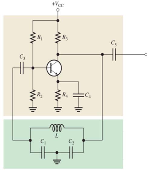
122 Conditions for Barkhausen criterion According to Barkhausen criterion for sustained oscillation: The magnitude of the product of open loop gain of the amplifier and the magnitude of the feedback factor is unity, i.e., βa =1 βa =1 where A is the gain of the amplifying element in the circuit and β(jω)β(jω) is the transfer function of the feedback path. The total phase shift around the loop is 00 or integral multiples of 2π2π.
123 Tank Circuit LC parallel circuit is called tank circuit. Once excited, it oscillates at
124
125 The energy keeps oscillating between electric potential energy and magnetic filed energy
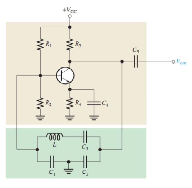
126 Damped oscillations are produced.
127
128 RC OSCILLATORS Three types of feedback oscillators that use RC circuits to produce sinusoidal outputs are the o Wien-bridge oscillator o Phase-shift oscillator o Twin-T oscillator -Generally, RC feedback oscillators are used for frequencies up to about 1 MHz. -The Wien-bridge is by far the most widely used type of RC feedback oscillator for this range of frequencies.
129 RC Phase Shift Oscillator
130 The phase shift oscillator utilizes three RC circuits to provide 180º phase shift that when coupled with the 180º of the op-amp itself provides the necessary feedback to sustain oscillations. The gain must be at least 29 to maintain the oscillations. The frequency of resonance for the this type is similar to any RC circuit oscillator.
131 Wien bridge oscillator
132 Wien bridge oscillator The Wien bridge oscillator is essentially a feedback amplifier in which the Wien bridge serves as the phase-shift network. The Wien bridge is an ac bridge, the balance of which is achieved at one particular frequency. Frequency of Oscillation
133 LC Oscillators Colpitts Oscillator Hartley Oscillator Clapp Oscillator Franklin Oscillator Armstrong Oscillator Miller Oscillator
134 Colpitts Oscillator
135 One basic type of resonant circuit feedback oscillator is the Colpitts oscillator. This type of oscillator uses an LC circuit in the feedback loop to provide the necessary phase shift and to act as a resonant filter that passes only the desired frequency of oscillation. The approximate frequency of oscillation is the resonant frequency of the LC circuit and is established by the values of C1,C2,L and according to the formula:
136 Where CT is the total capacitance. Because the capacitors effectively appear in series around the tank circuit, the total capacitance CT is

137 The Hartley Oscillator
138 The Hartley Oscillator The Hartley oscillator is similar to the Colpitts except that the feedback circuit consists of two series inductors and a parallel capacitor In this circuit, the frequency of oscillation for(q>10) is Where LT=L1+L2
139 The Clapp Oscillator
140 The Clapp Oscillator The Clapp oscillator is a variation of the Colpitts. The basic difference is an additional capacitor C3,in series with the inductor in the resonant feedback circuit Since C3 is in series with C1 and C2 around the tank circuit, the total capacitance is and the approximate frequency of oscillation (Q>10) is
141 The Armstrong Oscillator
142 The Armstrong Oscillator This type of LC feedback oscillator uses transformer coupling to feed back a portion of the signal voltage. The transformer secondary coil provides the feedback to keep the oscillation going. The Armstrong is less common than the Colpitts, Clapp, and Hartley, mainly because of the disadvantage of transformer size and cost. The frequency of oscillation is set by the inductance of the primary winding(lpri) in parallel with C1.
143 Franklin Oscillator
144 Franklin Oscillator The Franklin Oscillator has 2 CE amplifier stages which gives phase shift from input to output. The frequency of oscillation is
145 Quartz Crystal
146 Quartz Crystal A quartz crystal exhibits a very important property known as the piezoelectric effect. When a mechanical pressure is applied across the faces of the crystal, a voltage which is proportional to mechanical pressure appears across the crystal. That voltage causes distortion in the crystal. Distorted amount will be proportional to the applied voltage and also an alternate voltage applied to a crystal it causes to vibrate at its natural frequency.
147 Quartz Crystal Oscillator
148 Quartz Crystal Oscillator The quartz crystal oscillator circuit diagram consists of two resonances such as series and parallel resonance, i.e., two resonant frequencies The series resonance occurs when the reactance produced by capacitance C1is equal and opposite to the reactance produced by inductance L.
149 UNIT IV TUNED AMPLIFIERS & MULTIVIBRATOR CIRCUITS Tank circuits. Analysis of single tuned amplifier, Double tuned, stagger tuned amplifiers. Instability of tuned amplifiers, stabilization techniques, Narrow band neutralization using coil, Broad banding using Hazeltine neutralization, Class C tuned amplifiers and their applications. Efficiency of Class C tuned Amplifier. Astable multivibrators, monostable and bistable multivibrator using similar and complementary transistors, speed up capacitors,schmitt trigger circuits.
150 Tuned Amplifier Definition An amplifier circuit in which the load circuit is a tank circuit such that it can be tuned to pass or amplify selection of a desired frequency or a narrow band of frequencies, is known as Tuned Circuit Amplifier.
151 Tuned Amplifier Characteristics Tuned amplifier selects and amplifies a single frequency from a mixture of frequencies in any frequency range. A Tuned amplifier employs a tuned circuit. It uses the phenomena of resonance, the tank circuit which is capable of selecting a particular or relative narrow band of frequencies. The centre of this frequency band is the resonant frequency of the tuned circuit. Both types consist of an inductance L and capacitance C with two element connected in series and parallel
152 Resonance Circuits When at particular frequency the inductive reactance became equal to capacitive reactance and the circuit then behaves as purely resistive circuit. This phenomenon is called the resonance and the corresponding frequency is called the resonant frequency. C L Tuned circuit
153 Classification of Tuned Amplifier
154 Single Tuned Amplifiers
155 Single Tuned Amplifier
156 Single Tuned Amplifier Single Tuned Amplifier consist of only one Tank Circuit and the amplifing frequency range is Determined by it. By giving signal to its input terminal of various Frequency Ranges. The Tank Circuit on its collector delivers High Impedence on resonant Frequency. Thus the amplified signal is Completely Available on the output Terminal. And for input signals other than Resonant Frequency, the tank circuit provides lower imedence, hence most of the signals get attenuated at collector Terminal.
157 Limitations This tuned amplifier are required to be highly selective. But high selectivity required a tuned circuit with a high Q- factor. A high Q- factor circuit will give a high A v but at the same time, it will give much reduced band with because bandwidth is inversely proportional to the Q- factor. It means that tuned amplifier with reduce bandwidth may not be able to amplify equally the complete band of signals & result is poor reproduction. This is called potential instability in tuned amplifier.
158 Double tuned amplifier
159 Double tuned amplifier Double tuned amplifiers consists of Inductively coupled two tuned circuits. One L1, C1 and the other L2, C2. In the Collector terminals. A change in the coupling of the two tuned circuits results in change in the shape of the Frequency response curve. By proper adjustment of the coupling between the two coils of the two tuned circuits, the required results(high selectivity, high Voltage gain and required bandwidth) may be obtained.
160 Resonance curve of Parallel Resonant circuit: Voltage gain A V K=2 f r Loose coupling K=1 K=1.5 Critical coupling Frequency f r
161 Stagger Tuned Amplifier
162 Stagger Tuned Amplifier Stagger Tuned Amplifiers are used to improve the overall frequency response of tuned Amplifiers. Stagger tuned Amplifiers are usually designed so that the overall response exhibits maximal flatness around the centre frequency. It needs a number of tuned circuit operating in union. The overall frequency response of a Stagger tuned amplifier is obtained by adding the individual response together. Since the resonant Frequencies of different tuned circuits are displaced or staggered, they are referred as Stagger Tuned Amplifier.
163 The main advantage of stagger tuned amplifier is increased bandwidth. Its Drawback is Reduced Selectivity and critical tuning of many tank circuits. They are used in RF amplifier stage in Radio Receivers. The stagger tuning in this circuit is achieved by resonating the tuned circuits L1 C1, L2 C2 to slightly different Frequencies
164 Stagger Tuned Amplifier Voltage Freq. response of first stage f 1 f 0 f 2 Frequency Freq. response of second stage Over all response
165 Neutralization using coil
166 Neutralization using coil L part of the tuned circuit at the base o next stage is oriented or minimum coupling to the other winding. It is wound on a separate from and is mounted at right angle to the coupled windings. If the windings are properly polarized, the voltage across L due to the circulating current in the base circuit will have the proper phase to cancel the signal coupled through the base to collector, C bc capacitance.
167 Hazeltine Neutralization
168 Hazeltine Neutralization In this circuit a small value of variable capacitance C N is connected from the bottom of coil, point B, to the base. Therefore, the internal capacitance C bc, shown dotted, feeds a signal from the top end of the coil, point A, to the transistor base and the C N feeds a signal output equal magnitude but opposite polarity from the bottom output coil, point B, to the base. The neutralizing capacitor, C N can be adjusted correctly to completely nullify the signal fed through the C bc
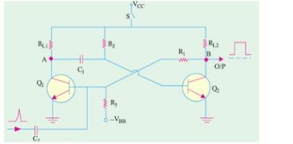
169 Class C Tuned Amplifier Class C amplifiers are biased so that conduction occurs for much less than 180 degrees. Class C amplifiers are more efficient than either class A or push-pull class B and class AB, which means that more output power can be obtained from class C operation. The output amplitude is a nonlinear function of the input, so class C amplifiers are not used for linear amplification. They are generally used in radio frequency (RF) applications, including circuits, such as oscillators, that have a constant output amplitude modulators, where a high-frequency signal is controlled by a low-frequency signal. Therefore, Class C amplifiers are also called Tuned Amplifiers.
170 Class C Tuned Amplifier
171 Class C Tuned Amplifier Because the collector voltage (output) is not a replica of the input, the resistively loaded class C amplifier alone is of no value in linear applications. It is therefore necessary to use a class C amplifier with a parallel resonant circuit (tank). The short pulse of collector current on each cycle of the input initiates and sustains the oscillation of the tank circuit so that an output sinusoidal voltage is produced. The tank circuit has high impedance only near the resonant frequency, so the gain is large only at this frequency
172 Sharpness of the Resonance Curve The resonance curve is required to be as sharp as possible in order to provide a high selectivity. A sharp resonance curve means that the impedance falls off rapidly as the frequency is varied above and below the resonant frequency.

173 Effect of Coil Resistance (R) on sharpness of the resonant curve
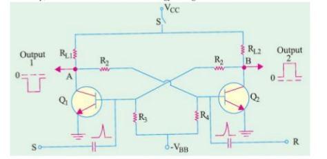
174 Applications of Tuned Amplifiers Tuned amplifiers serve the best for two purposes: a)selection of desired frequency. b)amplifying the signal to a desired level.
175 Advantages It provides high selectivity. It has small collector voltage. Power loss is also less. Signal to noise ratio of O/P is good. They are well suited for radio transmitters and receivers
176 Disadvantages They are not suitable to amplify audio frequencies. If the band of frequency is increase then design becomes complex. Since they use inductors and capacitors as tuning elements, the circuit is bulky and costly.
177 Multivibrators A Multivibrator is an electronic circuit that generates square, rectangular, pulse waveforms, also called nonlinear oscillators or function generators. Multivibrator is basically a two amplifier circuits arranged with regenerative feedback.
178 There are three types of Multivibrator: Astable Multivibrator: Circuit is not stable in either state it continuously oscillates from one state to the other. (Application in Oscillators) Monostable Multivibrator: One of the state is stable but the other is not. (Application in Timer) Bistable Multivibrator: Circuit is stable in both the state and will remain in either state indefinitely. The circuit can be flipped from one state to the other by an external event or trigger. (Application in Flip flop)
179 Duty Cycle Duty cycle is defined as the ratio of pulse duration to pulse period. The pulse duration is τ; this is how long the pulse remains high (amplitude=1 in the figure).the pulse period is T ; this is the duration of one complete cycle, and is just the inverse of the frequency in Hz (f = 1/T). D= τ / T
180 Astable Multivibrator The astable circuit has no stable state. With no external signal applied, the transistors alternately switch from cutoff to saturation at a frequency determined by the RC time constants of the coupling circuits. Astable multivibrator circuit consist of two cross coupled RC amplifiers.
181 Consists of two amplifying devices cross-coupled by resistors and capacitors. Typically, R2 = R3, R1 = R4, C1 = C2 and R2 >> R1. The circuit has two states State 1: VC1 LOW, VC2 HIGH, Q1 ON (saturation) and Q2 OFF. State 2: VC1 HIGH, VC2 LOW, Q1 OFF and Q2 ON (saturation). It continuously oscillates from one state to the other.
182 Astable Multivibrator
183 Monostable Multivibrators
184 Monostable Multivibrators One of the state is stable but the other is not. For that capacitive path between VC2 and VB1 removed. In stable state any one transistor conducts and other is off. Application of external trigger change the state. When the external signal goes high 8 VB2 charges up to VCC through R 2. After a certain time T, VB2=VON, Q2 turns on VC2 pulled to 0V, Q1 turns off. Enters state 1 and remains there When VB2 is momentarily pulled to ground by an external signal VC2 rises to VCC Q1 turns on VC1 pulled to 0V
185 Bistable Multivibrators
186 Bistable Multivibrators Both capacitors removed Stable for either state 1 or 2 Can be forced to either state by Set or Reset signals If Set is low, Q1 turns off VC1 (Vout) and VB2 rises towards VCC Q2 turns on
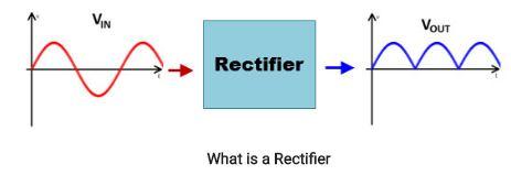
187 Bistable Multivibrators VC2 pulled to 0V VB1 is latched to 0V Circuit remains in state 2 until Reset is low If Reset is low Similar operation Circuit remains in state 1 until Set is low Behave as an RS flip-flop (memory element
188 Speed Up Capacitors Switching Characteristics can be improve by passing high frequency components of the pulses For this purpose small capacitances are used in shunt with the coupling resistorsr1. Due to this transition time reduces without affecting the stable states. These capacitors allows fast rise and fall times. Hence they are called as Speed Up Capacitors.
189 Speed Up Capacitors
190 Schmitt Trigger
191 Schmitt Trigger Schmitt trigger circuit converts any type of wave in to a rectangular wave. When power is first switched on it gives a small forward bias to Q2 then it comes in to conducting state.
192 This current flows through R4 which gives a potential drop VE across R4. This VE gives reverse bias to the base of Q1. So it comes to off state then the voltage across Q1 will be equal to Vcc, and voltage across Q2 approaches to zero. So in this case. a) Q1 is in cut off state and voltage across it is high. b) Q2 is in saturation or conducting state and voltage across it is low or zero..
193 Schmitt Trigger If the positive voltage of the sine wave from the signal generator is sufficient to over come the reverse bias of Q1, then Q1 comes in to conducting state and the negative going voltage is applied to the base of Q2 through R3. This reduces the forward bias of Q2 and thus Q2 comes in to cut-off state. Then the voltage across it is high and voltage across Q1 is low.
194 The same process repeats with opposite sense when negative half cycle if in put of a.c. is applied. The combined effect generates a rectangular wave at the out put. Also the frequency of the rectangular wave is equal to the frequency of the a.c. input signal. The amplitude of the in put voltage required to put Q2 in to conducting state is called lower trigger potential (LTP). Similarly input voltage required to put Q1 in to conducting state is called upper trigger potential (UTP).
195 Schmitt Trigger
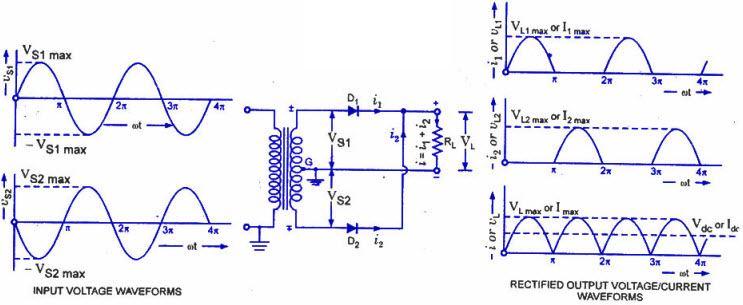
196 UNIT V RECTIFIERS, BLOCK OSCILLATORS AND TIMEBASE GENERATORS Half Wave Rectifier - Full Wave Rectifier Bridge Rectifier Performance of Rectifiers Filters Types of Filters L, C, LC, π Filters Ripple Factor Calculation for C, L, LC and π Filter Regulators Shunt and Series Voltage Regulator IC Regulator SMPS Power Control using SCR. RC and RL wave shaping circuits, UJT sawtooth generators, Linearization using constant current circuit, Bootstrap and Miller saw tooth generators, current time base generators, Time base circuits - Voltage-Time base circuit, Current-Time base circuit.
197
198 Definition Rectifiers A rectifier is an electrical device that converts AC supply into unidirectional DC supply. This process of converting alternating current (AC) to direct current (DC) is also called as rectification. These bridge rectifiers are available in different packages as modules ranging from few amperes to several hundred amperes. Mostly in bridge rectifier circuits, semiconductor diode is used for converting AC since it allows the current flow in one direction only (Unidirectional device)
199
200
201 Half Wave Rectifier It is a simple type of rectifier made with single diode which is connected in series with load. For small power levels this type of rectifier circuit is commonly used.
202 During the positive half of the AC input, diode becomes forward biased and currents starts flowing through it. During the negative half of the AC input, diode becomes reverse biased and current stops flowing through it. Output waveform across the load is shown in figure. Because of high ripple content in the output, this type of rectifier is seldom used with pure resistive load.
203 The output DC voltage of a half wave rectifier can be calculated with the following two ideal equations
204 Half wave rectifier
205 Half wave rectifier
206 Advantage Simple circuit and low cost Disadvantage The output current in the load contains, in addition to dc component, ac components of basic frequency equal to that of the input voltage frequency. Ripple factor is high and an elaborate filtering is, therefore, required to give steady dc output. The power output and, therefore, rectification efficiency is quite low. This is due to the fact that power is delivered only half the time. Transformer Utilization Factor (TUF) is low. DC saturation of transformer core resulting in magnetizing current and hysteresis losses and generation of harmonics.
207 Full Wave Center-tapped Rectifier This type of rectifier uses two diodes and a transformer with center tapped secondary winding. During the positive half cycle of the input AC diode D1 is forward biased and the current starts flowing to the load through it. During the negative half of the input diode D2 forward biased and D1 becomes reverse biased. Load current start flowing through D2 during this negative peak. Note that the current flow through load has not changed even when the voltage polarity changed.
208
209 Full Wave Bridge Rectifier Using the same secondary voltage, this bridge rectifier can produce almost double the output voltage as compared with full wave center-tapped transformer rectifier. During the positive half of the input AC diodes D1 and D2 are forward biased and D3 and D4 are reverse biased. Thus load current flows through D1 and D2 diodes. During the negative half cycle of the input diodes D3&D4 are forward biased and D1&D2 are reverse biased. Therefore load current flows through D3&D4 diodes.
210
211
212
213
214
215
216 Advantages of bridge rectifier The rectification efficiency of full-wave rectifier is double of that of a half-wave rectifier. Higher output voltage, higher output power and higher Transformer Utilization Factor in case of full-wave rectifier. The ripple voltage is low and of higher frequency in case of full-wave rectifier so simple filtering circuit is required No center tap is required in the transformer secondary so in case of a bridge rectifier the transformer required is simpler.
217 If stepping up or stepping down of voltage is not required, transformer can be eliminated even. For a given power output, power transformer of smaller size can be used in case of the bridge rectifier because current in both primary and secondary windings of the supply transformer flow for the entire ac cycle 2 Disadvantages of Bridge Rectifier It requires four diodes. The use of two extra diodes cause an additional voltage drop thereby reducing the output voltage.
218 Filters A filter circuit is a device to remove the AC components of the rectified output,but allow the DC component to reach the load. A filter circuit consists of passive circuit elements i.e inductors,capacitors,resistors and their combination.
219 Types of Filters Inductor Filter Capacitor Filter LC Filter ᴨ Filter
220 Inductor Filter
221 Inductor Filter Also called Choke Filter. Consists of an inductor L which is inserted between the Rectifier and the load resistance RL. Rectifier contains AC as well as DC components When output passes through inductor it offers a high resistance to the AC component and no resistance to DC component. Therefore AC components of the rectified output is blocked and only DC components reached at the load.
222 Capacitor Filter
223 Capacitor Filter Capacitor is connected across the load. During the rise of voltage it gets charge and is supplied to the load during the fall in voltage cycle. This process is repeated for each cycle and thus the repel is reduced across the load.
224 LC Filter
225 LC Filter Choke is connected in series with load. Offers high resistance to the AC components and allows DC component to flow through the load. The capacitor across the load is connected in parallel which filter out any AC component flowing through the choke.
226 CLC or PIE Filter
227 CLC or PIE Filter Three components are arranged in shape of Greek letter Pi. Input capacitor is selected to offer very low reactance to the repel frequency. Major part of filtering is done by C1. Remaining parts of repels are removed by the combining action of L and C2. It gives much better filter than LC filter.
228 Voltage Regulators A voltage regulator is used to regulate voltage level. When a steady, reliable voltage is needed, then voltage regulator is the preferred device. It generates a fixed output voltage that remains constant for any changes in an input voltage or load conditions. It acts as a buffer for protecting components from damages.

229 Block Diagram
230 Types of Voltage Regulators Series Voltage Regulator Shunt Voltage Regulator

231 Series Voltage Regulator
232 Series Voltage Regulator A control element is placed to collect the unregulated input which controls the magnitude of the input voltage and passes it to the output. The output voltage is then fedback to a sampling circuit and then compared with a reference voltage and sent back to the output. If the output voltage tends to increase the comparator circuit provides a control signal to cause the control element to reduce the magnitude of the output voltage by passing it through the sampling circuit and comparing it, thereby maintaining a constant and steady output voltage.
233

234 Shunt Voltage Regulator
235 Shunt Voltage Regulator If the output voltage increases, the shunt current increases and thus produces less load current and maintains a regulated output voltage. If the output voltage reduces, the shunt current reduces and thus produces more load current and maintains a regulated constant output voltage.
236 IC Regulator IC Voltage Regulator uses integrated circuits for voltage regulation. One advantage of IC voltage regulator is that properties like thermal compensation, short circuit protection and surge protection can be built into the device. Most of the commonly used IC voltage regulators are three-terminal devices

237 IC Regulator
238 Switched Mode Power Supply A switched-mode power supply (SMPS) is an electronic circuit that converts power using switching devices that are turned on and off at high frequencies, and storage components such as inductors or capacitors to supply power when the switching device is in its non-conduction state. Switching power supplies have high efficiencies and are widely used in a variety of electronic equipment, including computers and other sensitive equipment requiring stable and efficient power supply.
239 Switched Mode Power Supply Switched-mode power supplies are classified according to the type of input and output voltages. The four major categories are: AC to DC,DC to DC,DC to AC,AC to AC A basic isolated AC to DC switched-mode power supply consists of: Input rectifier and filter Inverter consisting of switching devices such as MOSFETs,Transformer,Output rectifier and filter Feedback and control circuit

240 Switched Mode Power Supply
LARGE SIGNAL AMPLIFIERS
 LARGE SIGNAL AMPLIFIERS One method used to distinguish the electrical characteristics of different types of amplifiers is by class, and as such amplifiers are classified according to their circuit configuration
TUNED AMPLIFIERS. Tank circuits.
 Tank circuits. TUNED AMPLIFIERS Analysis of single tuned amplifier, Double tuned, stagger tuned amplifiers. Instability of tuned amplifiers, stabilization techniques, Narrow band neutralization using coil,
EC202- ELECTRONIC CIRCUITS II Unit- I -FEEEDBACK AMPLIFIER
 EC202- ELECTRONIC CIRCUITS II Unit- I -FEEEDBACK AMPLIFIER 1. What is feedback? What are the types of feedback? 2. Define positive feedback. What are its merits and demerits? 3. Define negative feedback.
Power Amplifiers. Class A Amplifier
 Power Amplifiers The Power amplifiers amplify the power level of the signal. This amplification is done in the last stage in audio applications. The applications related to radio frequencies employ radio
Oscillators. An oscillator may be described as a source of alternating voltage. It is different than amplifier.
 Oscillators An oscillator may be described as a source of alternating voltage. It is different than amplifier. An amplifier delivers an output signal whose waveform corresponds to the input signal but
NOORUL ISLAM COLLEGE OF ENGG, KUMARACOIL. DEPARTMENT OF ELECTRONICS AND COMMUNICATION ENGG. SUBJECT CODE: EC 1251 SUBJECT NAME: ELECTRONIC CIRCUITS-II
 NOORUL ISLAM COLLEGE OF ENGG, KUMARACOIL. DEPARTMENT OF ELECTRONICS AND COMMUNICATION ENGG. SUBJECT CODE: EC 1251 SUBJECT NAME: ELECTRONIC CIRCUITS-II Prepared by, C.P.SREE BALA LEKSHMI (Lect/ECE) ELECTRONICS
UNIT I - TRANSISTOR BIAS STABILITY
 UNIT I - TRANSISTOR BIAS STABILITY OBJECTIVE On the completion of this unit the student will understand NEED OF BIASING CONCEPTS OF LOAD LINE Q-POINT AND ITS STABILIZATION AND COMPENSATION DIFFERENT TYPES
SIDDHARTH GROUP OF INSTITUTIONS :: PUTTUR (AUTONOMOUS) Siddharth Nagar, Narayanavanam Road QUESTION BANK
 Siddharth Nagar, Narayanavanam Road QUESTION BANK") SIDDHARTH GROUP OF INSTITUTIONS :: PUTTUR (AUTONOMOUS) Siddharth Nagar, Narayanavanam Road 517583 QUESTION BANK Subject with Code : Electronic Circuit Analysis (16EC407) Year & Sem: II-B.Tech & II-Sem
SIDDHARTH GROUP OF INSTITUTIONS :: PUTTUR (AUTONOMOUS) Siddharth Nagar, Narayanavanam Road 517583 QUESTION BANK Subject with Code : Electronic Circuit Analysis (16EC407) Year & Sem: II-B.Tech & II-Sem
BHARATHIDASAN ENGINEERING COLLEGE
 BHARATHIDASAN ENGINEERING COLLEGE DEPARTMENT OF ELECTRONICS AND COMMUNICATION ENGINEERING EC6401 - ELECTRONIC CIRCUITS - II QUESTION BANK II- YEAR IV SEM ACDEMIC YEAR: 2016-2017 EVEN SEMESTER EC6401 ELECTRONIC
Subject Code: Model Answer Page No: / N
 Important Instructions to examiners: 1) The answers should be examined by key words and not as word-to-word as given in the model answer scheme. 2) The model answer and the answer written by candidate
MAHALAKSHMI ENGINEERING COLLEGE TIRUCHIRAPALLI UNIT III TUNED AMPLIFIERS PART A (2 Marks)
") MAHALAKSHMI ENGINEERING COLLEGE TIRUCHIRAPALLI-621213. UNIT III TUNED AMPLIFIERS PART A (2 Marks) 1. What is meant by tuned amplifiers? Tuned amplifiers are amplifiers that are designed to reject a certain
MAHALAKSHMI ENGINEERING COLLEGE TIRUCHIRAPALLI-621213. UNIT III TUNED AMPLIFIERS PART A (2 Marks) 1. What is meant by tuned amplifiers? Tuned amplifiers are amplifiers that are designed to reject a certain
Question Bank EC6401 ELECTRONIC CIRCUITS - II
 FATIMA MICHAEL COLLEGE OF ENGINEERING & TECHNOLOGY Madurai Sivagangai Main Road Madurai - 625 020. [An ISO 9001:2008 Certified Institution] SEMESTER: IV / ECE Question Bank EC6401 ELECTRONIC CIRCUITS -
The steeper the phase shift as a function of frequency φ(ω) the more stable the frequency of oscillation
 the more stable the frequency of oscillation") It should be noted that the frequency of oscillation ω o is determined by the phase characteristics of the feedback loop. the loop oscillates at the frequency for which the phase is zero The steeper the
It should be noted that the frequency of oscillation ω o is determined by the phase characteristics of the feedback loop. the loop oscillates at the frequency for which the phase is zero The steeper the
VALLIAMMAI ENGINEERING COLLEGE
 VALLIAMMAI ENGINEERING COLLEGE SRM Nagar, Kattankulathur 603 203. DEPARTMENT OF ELECTRONICS & COMMUNICATION ENGINEERING SUBJECT QUESTION BANK : EC6401 ELECTRONICS CIRCUITS-II SEM / YEAR: IV / II year B.E.
UNIT 1 MULTI STAGE AMPLIFIES
 UNIT 1 MULTI STAGE AMPLIFIES 1. a) Derive the equation for the overall voltage gain of a multistage amplifier in terms of the individual voltage gains. b) what are the multi-stage amplifiers? 2. Describe
DEPARTMENT OF ELECTRONICS AND COMMUNICATION ENGINEERING III SEMESTER EC 6304 ELECTRONIC CIRCUITS I. (Regulations 2013)
") DEPARTMENT OF ELECTRONICS AND COMMUNICATION ENGINEERING III SEMESTER EC 6304 ELECTRONIC CIRCUITS I (Regulations 2013 UNIT-1 Part A 1. What is a Q-point? [N/D 16] The operating point also known as quiescent
DEPARTMENT OF ELECTRONICS AND COMMUNICATION ENGINEERING III SEMESTER EC 6304 ELECTRONIC CIRCUITS I (Regulations 2013 UNIT-1 Part A 1. What is a Q-point? [N/D 16] The operating point also known as quiescent
Chapter.8: Oscillators
 Chapter.8: Oscillators Objectives: To understand The basic operation of an Oscillator the working of low frequency oscillators RC phase shift oscillator Wien bridge Oscillator the working of tuned oscillator
Scheme Q.1 Attempt any SIX of following: 12-Total Marks a) Draw symbol NPN and PNP transistor. 2 M Ans: Symbol Of NPN and PNP BJT (1M each)
 Draw symbol NPN and PNP transistor. 2 M Ans: Symbol Of NPN and PNP BJT (1M each)") Q. No. WINTER 16 EXAMINATION (Subject Code: 17319) Model Answer Important Instructions to examiners: 1) The answers should be examined by key words and not as word-to-word as given in the model answer
Q. No. WINTER 16 EXAMINATION (Subject Code: 17319) Model Answer Important Instructions to examiners: 1) The answers should be examined by key words and not as word-to-word as given in the model answer
TUNED AMPLIFIERS 5.1 Introduction: Coil Losses:
 TUNED AMPLIFIERS 5.1 Introduction: To amplify the selective range of frequencies, the resistive load R C is replaced by a tuned circuit. The tuned circuit is capable of amplifying a signal over a narrow
Table of Contents Lesson One Lesson Two Lesson Three Lesson Four Lesson Five PREVIEW COPY
 Oscillators Table of Contents Lesson One Lesson Two Lesson Three Introduction to Oscillators...3 Flip-Flops...19 Logic Clocks...37 Lesson Four Filters and Waveforms...53 Lesson Five Troubleshooting Oscillators...69
Lab 4 : Transistor Oscillators
 Objective: Lab 4 : Transistor Oscillators In this lab, you will learn how to design and implement a colpitts oscillator. In part II you will implement a RC phase shift oscillator Hardware Required : Pre
EE301 ELECTRONIC CIRCUITS CHAPTER 2 : OSCILLATORS. Lecturer : Engr. Muhammad Muizz Bin Mohd Nawawi
 EE301 ELECTRONIC CIRCUITS CHAPTER 2 : OSCILLATORS Lecturer : Engr. Muhammad Muizz Bin Mohd Nawawi 2.1 INTRODUCTION An electronic circuit which is designed to generate a periodic waveform continuously at
DHANALAKSHMI COLLEGE OF ENGINEERING DEPARTMENT OF ELECTRICAL AND ELECTRONICS ENGINEERING EC6202 ELECTRONIC DEVICES AND CIRCUITS
 DHANALAKSHMI COLLEGE OF ENGINEERING DEPARTMENT OF ELECTRICAL AND ELECTRONICS ENGINEERING EC6202 ELECTRONIC DEVICES AND CIRCUITS UNIT-I - PN DIODEAND ITSAPPLICATIONS 1. What is depletion region in PN junction?
MARIA COLLEGE OF ENGINEERING AND TECHNOLOGY, ATTOOR UNIT-1. Feedback Amplifiers
 MARIA COLLEGE OF ENGINEERING AND TECHNOLOGY, ATTOOR DEPARTMENT OF ELECTRONICS AND COMMUNICATION ENGINEERING ELECTRONIC CIRCUITS-II 2 MARKS QUESTIONS & ANSWERS UNIT-1 Feedback Amplifiers 1. What is meant
OBJECTIVE TYPE QUESTIONS
 OBJECTIVE TYPE QUESTIONS Q.1 The breakdown mechanism in a lightly doped p-n junction under reverse biased condition is called (A) avalanche breakdown. (B) zener breakdown. (C) breakdown by tunnelling.
FREQUENTLY ASKED QUESTIONS
 FREQUENTLY ASKED QUESTIONS UNIT-1 SUBJECT : ELECTRONIC DEVICES AND CIRCUITS SUBJECT CODE : EC6202 BRANCH: EEE PART -A 1. What is meant by diffusion current in a semi conductor? (APR/MAY 2010, 2011, NOV/DEC
EC6202-ELECTRONIC DEVICES AND CIRCUITS YEAR/SEM: II/III UNIT 1 TWO MARKS. 1. Define diffusion current.
 EC6202-ELECTRONIC DEVICES AND CIRCUITS YEAR/SEM: II/III UNIT 1 TWO MARKS 1. Define diffusion current. A movement of charge carriers due to the concentration gradient in a semiconductor is called process
State the application of negative feedback and positive feedback (one in each case)
") (ISO/IEC - 700-005 Certified) Subject Code: 073 Model wer Page No: / N Important Instructions to examiners: ) The answers should be examined by key words and not as word-to-word as given in the model answer
(ISO/IEC - 700-005 Certified) Subject Code: 073 Model wer Page No: / N Important Instructions to examiners: ) The answers should be examined by key words and not as word-to-word as given in the model answer
MAHALAKSHMI ENGINEERING COLLEGE TIRUCHIRAPALLI
 MAHALAKSHMI ENGINEERING COLLEGE TIRUCHIRAPALLI-621213. QUESTION BANK DEPARTMENT: EEE SUBJECT CODE: EE2203 SEMESTER : III SUBJECT NAME: ELECTRONIC DEVICES &CIRCUITS UNIT 4-AMPLIFIERS AND OSCILLATORS PART
UNIT 4 BIASING AND STABILIZATION
 UNIT 4 BIASING AND STABILIZATION TRANSISTOR BIASING: To operate the transistor in the desired region, we have to apply external dec voltages of correct polarity and magnitude to the two junctions of the
Difference between BJTs and FETs. Junction Field Effect Transistors (JFET)
") Difference between BJTs and FETs Transistors can be categorized according to their structure, and two of the more commonly known transistor structures, are the BJT and FET. The comparison between BJTs
Difference between BJTs and FETs Transistors can be categorized according to their structure, and two of the more commonly known transistor structures, are the BJT and FET. The comparison between BJTs
Expect to be successful, expect to be liked,
 Thought of the Day Expect to be successful, expect to be liked, expect to be popular everywhere you go. Oscillators 1 Oscillators D.C. Kulshreshtha Oscillators 2 Need of an Oscillator An oscillator circuit
MAHARASHTRA STATE BOARD OF TECHNICAL EDUCATION (Autonomous) (ISO/IEC Certified) Summer 2016 EXAMINATIONS.
 (ISO/IEC Certified) Summer 2016 EXAMINATIONS.") Summer 2016 EXAMINATIONS Subject Code: 17321 Model Answer Important Instructions to examiners: 1) The answers should be examined by key words and not as word-to-word as given in the answer scheme. 2) The
Summer 2016 EXAMINATIONS Subject Code: 17321 Model Answer Important Instructions to examiners: 1) The answers should be examined by key words and not as word-to-word as given in the answer scheme. 2) The
Small signal Amplifier stages. Figure 5.2 Classification of power amplifiers
 5.1 Introduction When the power requirement to drive the load is in terms of several Watts rather than mili-watts the power amplifiers are used. Power amplifiers form the last stage of multistage amplifiers.
GATE: Electronics MCQs (Practice Test 1 of 13)
") GATE: Electronics MCQs (Practice Test 1 of 13) 1. Removing bypass capacitor across the emitter leg resistor in a CE amplifier causes a. increase in current gain b. decrease in current gain c. increase
GATE: Electronics MCQs (Practice Test 1 of 13) 1. Removing bypass capacitor across the emitter leg resistor in a CE amplifier causes a. increase in current gain b. decrease in current gain c. increase
INSTITUTE OF AERONAUTICAL ENGINEERING (AUTONOMUS) Dundigal, Hyderabad
 Dundigal, Hyderabad") INSTITUTE OF AERONAUTICAL ENGINEERING (AUTONOMUS) Dundigal, Hyderabad - 00 0 ELECTRONICS AND COMMUNICATION ENGINEERING ASSIGNMENT Name : ELECTRONIC CIRCUIT ANALYSIS Code : A0 Class : II - B. Tech nd semester
INSTITUTE OF AERONAUTICAL ENGINEERING (AUTONOMUS) Dundigal, Hyderabad - 00 0 ELECTRONICS AND COMMUNICATION ENGINEERING ASSIGNMENT Name : ELECTRONIC CIRCUIT ANALYSIS Code : A0 Class : II - B. Tech nd semester
Feedback Amplifier & Oscillators
 256 UNIT 5 Feedback Amplifier & Oscillators 5.1 Learning Objectives Study definations of positive /negative feedback. Study the camparions of positive and negative feedback. Study the block diagram and
Bipolar Junction Transistors
 Bipolar Junction Transistors Invented in 1948 at Bell Telephone laboratories Bipolar junction transistor (BJT) - one of the major three terminal devices Three terminal devices more useful than two terminal
THIRD SEMESTER DIPLOMA EXAMINATION IN ELECTRICAL & ELECTRONICS ENGINEERING, MARCH 2013 ELECTRONIC DEVICES AND CIRCUITS
 REVISION-2010 Reg. No SUB CODE:3053 Signature THIRD SEMESTER DIPLOMA EXAMINATION IN ELECTRICAL & ELECTRONICS ENGINEERING, MARCH 2013 ELECTRONIC DEVICES AND CIRCUITS Time :3hours Maximum marks:100 PART
TRANSISTOR BIASING AND STABILIZATION
 TRANSISTOR BIASING AND STABILIZATION 4.1 NEED FOR TRANSISTOR BIASING: If the o/p signal must be a faithful reproduction of the i/p signal, the transistor must be operated in active region. That means an
Chapter 6: Power Amplifiers
 Chapter 6: Power Amplifiers Contents Class A Class B Class C Power Amplifiers Class A, B and C amplifiers are used in transmitters Tuned with a band width wide enough to pass all information sidebands
Chapter 8. Field Effect Transistor
 Chapter 8. Field Effect Transistor Field Effect Transistor: The field effect transistor is a semiconductor device, which depends for its operation on the control of current by an electric field. There
LECTURE NOTES ELECTRONIC CIRCUITS II SYLLABUS
 FATIMA MICHAEL COLLEGE OF ENGINEERING & TECHNOLOGY Madurai Sivagangai Main Road Madurai - 625 020. [An ISO 9001:2008 Certified Institution] LECTURE NOTES EC6401 ELECTRONIC CIRCUITS - II SEMESTER: IV /
Crystal Oscillator. Circuit symbol
 Crystal Oscillator Crystal Oscillator Piezoelectric crystal (quartz) Operates as a resonant circuit Shows great stability in oscillation frequency Piezoelectric effect : When mechanical stress is applied
DEFINITION: Classification of oscillators Based on the frequency generated Oscillator type Frequency range
 DEFINITION: An oscillator is just an electronic circuit which converts dc energy into AC energy of required frequency. (Or) An oscillator is an electronic circuit which produces an ac output without any
(a) BJT-OPERATING MODES & CONFIGURATIONS
 BJT-OPERATING MODES & CONFIGURATIONS") (a) BJT-OPERATING MODES & CONFIGURATIONS 1. The leakage current I CBO flows in (a) The emitter, base and collector leads (b) The emitter and base leads. (c) The emitter and collector leads. (d) The base
(a) BJT-OPERATING MODES & CONFIGURATIONS 1. The leakage current I CBO flows in (a) The emitter, base and collector leads (b) The emitter and base leads. (c) The emitter and collector leads. (d) The base
AE103 ELECTRONIC DEVICES & CIRCUITS DEC 2014
 Q.2 a. State and explain the Reciprocity Theorem and Thevenins Theorem. a. Reciprocity Theorem: If we consider two loops A and B of network N and if an ideal voltage source E in loop A produces current
Transistor Biasing. DC Biasing of BJT. Transistor Biasing. Transistor Biasing 11/23/2018
 Transistor Biasing DC Biasing of BJT Satish Chandra Assistant Professor Department of Physics P P N College, Kanpur www.satish0402.weebly.com A transistors steady state of operation depends a great deal
UNIT I PN JUNCTION DEVICES
 UNIT I PN JUNCTION DEVICES 1. Define Semiconductor. 2. Classify Semiconductors. 3. Define Hole Current. 4. Define Knee voltage of a Diode. 5. What is Peak Inverse Voltage? 6. Define Depletion Region in
Code: 9A Answer any FIVE questions All questions carry equal marks *****
 II B. Tech II Semester (R09) Regular & Supplementary Examinations, April/May 2012 ELECTRONIC CIRCUIT ANALYSIS (Common to EIE, E. Con. E & ECE) Time: 3 hours Max Marks: 70 Answer any FIVE questions All
Summer 2015 Examination
 Summer 2015 Examination Subject Code: 17445 Model Answer Important Instructions to examiners: 1) The answers should be examined by key words and not as word-to-word as given in the model answer scheme.
Feedback and Oscillator Circuits
 Chapter 14 Chapter 14 Feedback and Oscillator Circuits Feedback Concepts The effects of negative feedback on an amplifier: Disadvantage Lower gain Advantages Higher input impedance More stable gain Improved
Emitter base bias. Collector base bias Active Forward Reverse Saturation forward Forward Cut off Reverse Reverse Inverse Reverse Forward
 SEMICONDUCTOR PHYSICS-2 [Transistor, constructional characteristics, biasing of transistors, transistor configuration, transistor as an amplifier, transistor as a switch, transistor as an oscillator] Transistor
SUMMER 13 EXAMINATION Subject Code: Model Answer Page No: / N
 Important Instructions to examiners: 1) The answers should be examined by key words and not as word-to-word as given in the model answer scheme. 2) The model answer and the answer written by candidate
Sub Code & Name: EC2251- ELECTRONIC CIRCUITS II Unit : I Branch : ECE Year:II
 Unit : I Branch : ECE Year:II Page 01 of 06 UNIT 1 FEEDBACK AMPLIFIERS 9 Block diagram, Loop gain, Gain with feedback, Effects of negative feedback Sensitivity and desensitivity of gain, Cut-off frequencies,
Multivibrators. Department of Electrical & Electronics Engineering, Amrita School of Engineering
 Multivibrators Multivibrators Multivibrator is an electronic circuit that generates square, rectangular, pulse waveforms. Also called as nonlinear oscillators or function generators. Multivibrator is basically
Document Name: Electronic Circuits Lab. Facebook: Twitter:
 Document Name: Electronic Circuits Lab www.vidyathiplus.in Facebook: www.facebook.com/vidyarthiplus Twitter: www.twitter.com/vidyarthiplus Copyright 2011-2015 Vidyarthiplus.in (VP Group) Page 1 CIRCUIT
Transistor Digital Circuits
 Recapitulation Transistor Digital Circuits The transistor Operating principle and regions Utilization of the transistor Transfer characteristics, symbols Controlled switch model BJT digital circuits MOSFET
CHAPTER 3: OSCILLATORS AND WAVEFORM-SHAPING CIRCUITS
 CHAPTER 3: OSCILLATORS AND WAVEFORM-SHAPING CIRCUITS In the design of electronic systems, the need frequently arises for signals having prescribed standard waveforms (e.g., sinusoidal, square, triangle,
Skyup's Media ELECTRONIC CIRCUIT ANALYSIS
 ELECTRONIC CIRCUIT ANALYSIS MALLAREDDY COLLEGE OF ENGINEERING AND TECHNOLOGY DEPARTMENT OF ELECTROINICS AND COMMUNICATION ENGINEERING Answer all the following questions: PART A: B.TECH II YEAR II SEMESTER
 VALLIAMMAI ENGINEERING COLLEGE SRM NAGAR, KATTANKULATHUR- 603 203 DEPARTMENT OF ELECTRONICS AND COMMUNICATION ENGINEERING EC6202- ELECTRONIC DEVICES AND CIRCUITS UNIT I PN JUNCTION DEVICES 1. Define Semiconductor.
EC1203: ELECTRONICS CIRCUITS-I UNIT-I TRANSISTOR BIASING PART-A
 SHRI ANGALAMMAN COLLEGE OF ENGG & TECH., TRICHY 621105 (Approved by AICTE, New Delhi and Affiliated to Anna University Chennai/Trichy) ( ISO 9001:2008 Certified Institution) DEPARTMENT OF ELECTRONICS &
MODEL ANSWER SUMMER 17 EXAMINATION 17319
 MODEL ANSWER SUMMER 17 EXAMINATION 17319 Subject Title: Electronics Devices and Circuits. Subject Code: Important Instructions to examiners: 1) The answers should be examined by key words and not as word-to-word
Gechstudentszone.wordpress.com
 8.1 Operational Amplifier (Op-Amp) UNIT 8: Operational Amplifier An operational amplifier ("op-amp") is a DC-coupled high-gain electronic voltage amplifier with a differential input and, usually, a single-ended
BJT Circuits (MCQs of Moderate Complexity)
") BJT Circuits (MCQs of Moderate Complexity) 1. The current ib through base of a silicon npn transistor is 1+0.1 cos (1000πt) ma. At 300K, the rπ in the small signal model of the transistor is i b B C r
BJT Circuits (MCQs of Moderate Complexity) 1. The current ib through base of a silicon npn transistor is 1+0.1 cos (1000πt) ma. At 300K, the rπ in the small signal model of the transistor is i b B C r
Operational Amplifiers
 Operational Amplifiers Table of contents 1. Design 1.1. The Differential Amplifier 1.2. Level Shifter 1.3. Power Amplifier 2. Characteristics 3. The Opamp without NFB 4. Linear Amplifiers 4.1. The Non-Inverting
Q1 A) Attempt any six: i) Draw the neat symbol of N-channel and P-channel FET
 Attempt any six: i) Draw the neat symbol of N-channel and P-channel FET") Subject Code:17319 Model Answer Page1 of 27 Important Instructions to examiners: 1) The answers should be examined by key words and not as word-to-word as given in the model answer scheme. 2) The model
Subject Code:17319 Model Answer Page1 of 27 Important Instructions to examiners: 1) The answers should be examined by key words and not as word-to-word as given in the model answer scheme. 2) The model
VALLIAMMAI ENGINEERING COLLEGE
 VALLIAMMAI ENGINEERING COLLEGE SRM Nagar, Kattankulathur 603 203 DEPARTMENT OF ELECTRONICS AND COMMUNICATION ENGINEERING QUESTION BANK IV SEMESTER EC6401 ELECTRONICS CIRCUITS-II Regulation 2013 Academic
Test Your Understanding
 074 Part 2 Analog Electronics EXEISE POBLEM Ex 5.3: For the switched-capacitor circuit in Figure 5.3b), the parameters are: = 30 pf, 2 = 5pF, and F = 2 pf. The clock frequency is 00 khz. Determine the
Oscillator Principles
 Oscillators Introduction Oscillators are circuits that generates a repetitive waveform of fixed amplitude and frequency without any external input signal. The function of an oscillator is to generate alternating
Dev Bhoomi Institute Of Technology Department of Electronics and Communication Engineering PRACTICAL INSTRUCTION SHEET REV. NO. : REV.
 Dev Bhoomi Institute Of Technology Department of Electronics and Communication Engineering PRACTICAL INSTRUCTION SHEET LABORATORY MANUAL EXPERIMENT NO. ISSUE NO. : ISSUE DATE: July 200 REV. NO. : REV.
Power Amplifiers. Introduction to Power Amplifiers. Amplifiers. Module
 Module 5 Amplifiers Introduction to What you ll learn in Module 5. Section 5.0 Introduction to. Understand the Operation of. Section 5.1 Power Transistors & Heat Sinks. Power Transistor Construction. Power
4. Forward bias of a silicon P-N junction will produce a barrier voltage of approximately how many volts? A. 0.2 B. 0.3 C. 0.7 D. 0.
 1. The dc current through each diode in a bridge rectifier equals A. the load current B. half the dc load current C. twice the dc load current D. one-fourth the dc load current 2. When matching polarity
Integrated Circuit: Classification:
 Integrated Circuit: It is a miniature, low cost electronic circuit consisting of active and passive components that are irreparably joined together on a single crystal chip of silicon. Classification:
EMT212 Analog Electronic II. Chapter 4. Oscillator
 EMT Analog Electronic II Chapter 4 Oscillator Objectives Describe the basic concept of an oscillator Discuss the basic principles of operation of an oscillator Analyze the operation of RC, LC and crystal
Electronic Circuits. Power Amplifiers. Manar Mohaisen Office: F208 Department of EECE
 Electronic Circuits Power Amplifiers Manar Mohaisen Office: F208 Email: manar.subhi@kut.ac.kr Department of EECE Review of the Precedent Lecture Explain the Amplifier Operation Explain the BJT AC Models
Figure 1: Closed Loop System
 SIGNAL GENERATORS 3. Introduction Signal sources have a variety of applications including checking stage gain, frequency response, and alignment in receivers and in a wide range of other electronics equipment.
 UNIVERSITY PART-A ANSWERS Unit-1 1. What is an amplifier? An amplifier is a device which produces a large electrical output of similar characteristics to that of the input parameters. 2. What are transistors?
So far we have dealt with only small-signal ampliers. In small-signal ampliers the main factors were amplication linearity gain
 Contents Power Amplier Types Class A Operation Class B Operation Class AB Operation Class C Operation Class D Operation Amplier Eciency Series-Fed Class A Amplier AC-DC Load Lines Maximum Eciency Figure
Linear electronic. Lecture No. 1
 1 Lecture No. 1 2 3 4 5 Lecture No. 2 6 7 8 9 10 11 Lecture No. 3 12 13 14 Lecture No. 4 Example: find Frequency response analysis for the circuit shown in figure below. Where R S =4kR B1 =8kR B2 =4k R
Chapter 13 Oscillators and Data Converters
 Chapter 13 Oscillators and Data Converters 13.1 General Considerations 13.2 Ring Oscillators 13.3 LC Oscillators 13.4 Phase Shift Oscillator 13.5 Wien-Bridge Oscillator 13.6 Crystal Oscillators 13.7 Chapter
LINEAR IC APPLICATIONS
 1 B.Tech III Year I Semester (R09) Regular & Supplementary Examinations December/January 2013/14 1 (a) Why is R e in an emitter-coupled differential amplifier replaced by a constant current source? (b)
OSCILLATORS AND WAVEFORM-SHAPING CIRCUITS
 OSILLATORS AND WAVEFORM-SHAPING IRUITS Signals having prescribed standard waveforms (e.g., sinusoidal, square, triangle, pulse, etc). To generate sinusoidal waveforms: o Positive feedback loop with non-linear
GOVERNMENT OF KARNATAKA KARNATAKA STATE PRE-UNIVERSITY EDUCATION EXAMINATION BOARD II YEAR PUC EXAMINATION MARCH-2012 SCHEME OF VALUATION
 GOVERNMENT OF KARNATAKA KARNATAKA STATE PRE-UNIVERSITY EDUCATION EXAMINATION BOARD II YEAR PUC EXAMINATION MARCH-0 SCHEME OF VALUATION Subject Code: 0 Subject: Qn. PART - A 0. Which is the largest of three
VETRI VINAYAHA COLLEGE OF ENGINEERING & TECHNOLOGY THOTTIAM, TIRUCHIRAPPALLI Department of Electronics and communication Engineering Question
 VETRI VINAYAHA COLLEGE OF ENGINEERING & TECHNOLOGY THOTTIAM, TIRUCHIRAPPALLI-621215 Department of Electronics and communication Engineering Question Bank EC6401: ELECTRONIC CIRCUITS II (Regulation 2013)
HIGH LOW Astable multivibrators HIGH LOW 1:1
 1. Multivibrators A multivibrator circuit oscillates between a HIGH state and a LOW state producing a continuous output. Astable multivibrators generally have an even 50% duty cycle, that is that 50% of
WINTER 14 EXAMINATION. Model Answer. 1) The answers should be examined by key words and not as word-to-word as given in the
 The answers should be examined by key words and not as word-to-word as given in the") WINTER 14 EXAMINATION Subject Code: 17213 Model Answer Important Instructions to examiners: 1) The answers should be examined by key words and not as word-to-word as given in the model answer scheme. 2)
WINTER 14 EXAMINATION Subject Code: 17213 Model Answer Important Instructions to examiners: 1) The answers should be examined by key words and not as word-to-word as given in the model answer scheme. 2)
Oscillators. Hartley, Colpitts, UJT relaxation. ECE/MEA Engg College S.R.K. 9/13/2007 Authored by: Ramesh.K
 Oscillators Hartley, Colpitts, UJT relaxation. S.R.K 9//007 Authored by: Ramesh.K This documents contains a brief note about the principle of sinusoidal oscillator and some general oscillator circuits
 Code No: Y0221/R07 Set No. 1 I B.Tech Supplementary Examinations, Apr/May 2013 BASIC ELECTRONIC DEVICES AND CIRCUITS (Electrical & Electronics Engineering) Time: 3 hours Max Marks: 80 Answer any FIVE Questions
Lesson Plan. Electronics 1-Total 51 Hours
 Lesson Plan. Electronics 1-Total 5s Unit I: Electrical Engineering materials:(10) Crystal structure & defects; Ceramic materials-structures, composites, processing and uses; Insulating laminates for electronics,
21/10/58. M2-3 Signal Generators. Bill Hewlett and Dave Packard s 1 st product (1939) US patent No HP 200A s schematic
 US patent No HP 200A s schematic") M2-3 Signal Generators Bill Hewlett and Dave Packard s 1 st product (1939) US patent No.2267782 1 HP 200A s schematic 2 1 The basic structure of a sinusoidal oscillator. A positive feedback loop is formed
M2-3 Signal Generators Bill Hewlett and Dave Packard s 1 st product (1939) US patent No.2267782 1 HP 200A s schematic 2 1 The basic structure of a sinusoidal oscillator. A positive feedback loop is formed
55:041 Electronic Circuits
 55:041 Electronic Circuits Oscillators Sections of Chapter 15 + Additional Material A. Kruger Oscillators 1 Stability Recall definition of loop gain: T(jω) = βa A f ( j) A( j) 1 T( j) If T(jω) = -1, then
Applied Electronics II
 Applied Electronics II Chapter 4: Wave shaping and Waveform Generators School of Electrical and Computer Engineering Addis Ababa Institute of Technology Addis Ababa University Daniel D./Getachew T./Abel
The Hartley Oscillator
 The Hartley Oscillator One of the main disadvantages of the basic LC Oscillator circuit we looked at in the previous tutorial is that they have no means of controlling the amplitude of the oscillations
CHAPTER 1 DIODE CIRCUITS. Semiconductor act differently to DC and AC currents
 CHAPTER 1 DIODE CIRCUITS Resistance levels Semiconductor act differently to DC and AC currents There are three types of resistances 1. DC or static resistance The application of DC voltage to a circuit
Video Course on Electronics Prof. D. C. Dube Department of Physics Indian Institute of Technology, Delhi
 Video Course on Electronics Prof. D. C. Dube Department of Physics Indian Institute of Technology, Delhi Module No. # 02 Transistors Lecture No. # 09 Biasing a Transistor (Contd) We continue our discussion
3 Circuit Theory. 3.2 Balanced Gain Stage (BGS) Input to the amplifier is balanced. The shield is isolated
 Input to the amplifier is balanced. The shield is isolated") Rev. D CE Series Power Amplifier Service Manual 3 Circuit Theory 3.0 Overview This section of the manual explains the general operation of the CE power amplifier. Topics covered include Front End Operation,
Rev. D CE Series Power Amplifier Service Manual 3 Circuit Theory 3.0 Overview This section of the manual explains the general operation of the CE power amplifier. Topics covered include Front End Operation,
This tutorial will suit all beginners who want to learn the fundamental concepts of transistors and transistor amplifier circuits.
 About the Tutorial An electronic signal contains some information which cannot be utilized if doesn t have proper strength. The process of increasing the signal strength is called as Amplification. Almost
An active filter offers the following advantages over a passive filter:
 ACTIVE FILTERS An electric filter is often a frequency-selective circuit that passes a specified band of frequencies and blocks or attenuates signals of frequencies outside this band. Filters may be classified
UNIT 2. Q.1) Describe the functioning of standard signal generator. Ans. Electronic Measurements & Instrumentation
 Describe the functioning of standard signal generator. Ans. Electronic Measurements & Instrumentation") UNIT 2 Q.1) Describe the functioning of standard signal generator Ans. STANDARD SIGNAL GENERATOR A standard signal generator produces known and controllable voltages. It is used as power source for the
UNIT 2 Q.1) Describe the functioning of standard signal generator Ans. STANDARD SIGNAL GENERATOR A standard signal generator produces known and controllable voltages. It is used as power source for the