EECE 2413 Electronics Laboratory
|
|
|
- Matilda Gilmore
- 6 years ago
- Views:
Transcription
1 EECE 2413 Electronics Laboratory Lab #5: MOSFETs and CMOS Goals This lab will introduce you to MOSFETs (metal-oxide-semiconductor field effect transistors). You will build a MOSFET inverter and determine the voltage transfer characteristic of this device (V out vs. V in ). From this transfer characteristic you will learn how to extract information about the MOSFET such as threshold voltage (V T ) and the device constant K. In the cutoff and triode regions the MOSFET approximates the operation of a switch. In between these two regions lies the saturation region. In saturation the MOSFET makes a good amplifier. Next, the CMOS inverter will be examined. This circuit also uses an n-channel MOSFET as the active driver, but replaces the drain resistor (R D ) with a p-channel MOSFET. This configuration dramatically reduces power consumption. As always, take your time during these experiments. Think about what you are being asked to do and why the experiments are important. Once you are comfortable with these basic MOSFET configurations, you will design and test either a CMOS logic gate or an AM radio transmitter using the CD4007 integrated circuit. Prelab Prelabs will be collected for grading at the beginning of the lab. Keep a copy for your own use during the lab! 1. In Fig. 3 find R G1 and R G2 such that V GS = 2 volts. Compute I D and V DS if V T = 1 volt and k n (W/L) = 0.5 ma/v 2 (see eqn in the 6th edition of Sedra and Smith). (If you only have the 2 nd edition of Hambley, refer to Section 5.3 and use the values of 1 volt for V to and K = 0.25 ma/v 2 in equation 5.18.) Remember that this is a DC analysis, so set v in = 0. (Note: there are many correct solutions for R G1 and R G2!) 2. Read the lab experiment and see the instructor with any questions you may have. 3. Read Part 2, choose one of the two design projects, and sketch a circuit you think will work. (You may change your design as you work through the lab, however.)
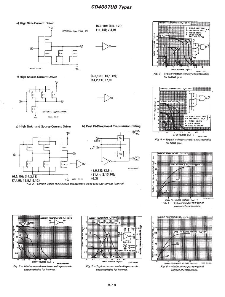
2 Part 1: MOSFET characteristics The MOSFETs that you will be using for this lab are in a 14-pin package as shown in Fig. 1. Study this diagram and become familiar with the layout of the individual MOSFETs within the CD4007 chip. Notice there are three n-channel devices and three p-channel devices. Although some devices share pins, all terminals for each device are available at an external pin on the chip. MOSFETs are actually 4-terminal devices: gate, drain, source, and substrate. In the CD4007 the substrates for all n-channel devices are connected to pin 7. Likewise, the substrates for all p-channel devices are connected to pin 14. For proper function of the MOSFETs you must attach pin 7 to the lowest potential in your circuit (usually ground) and you must attach pin 14 to the highest potential in your circuit (V DD ). MOSFETs are susceptible to electrostatic discharge (ESD). You have no doubt experienced large ESDs if you have ever scuffed your feet across a carpet and touched a metallic object. Even very small ESDs can damage a MOSFET by blowing-out the gate oxide. This is mainly because the gate oxide is very thin (<<100 nm). These MOSFETs have been protected from minor forms of ESD by two clamping diodes attached to each gate. One diode prevents V GS from exceeding V DD (pin 14) V. The other prevents V GS from becoming more negative than V SS ( pin 7) V. See fig. 1 on the spec sheet. V DD (highest voltage) 14 p p 8 n n p n 1 7 (lowest voltage) Figure 1. The CD4007 Integrated Circuit. 2
3 Concept: The DC transfer characteristic of a MOSFET inverter Build the simple MOSFET inverter shown in figure 2. You may use any of the three n-channel MOSFETs on the CD4007, but don t forget to connect pins 7 and 14 as described above! V DD R D G D S V Vout V in Figure 2. A MOSFET Inverter R D = 10 k, V DD = 10 V, 0 V in 10 V. a) Measure the voltage transfer characteristic for the MOSFET inverter by varying V in. Use the table below to guide you in selecting the appropriate data points. Important: Please time yourself, and record the time taken to complete step a). (This information will be used for comparison with MATLAB later in this experiment.) Table for Inverter Transfer Characteristic V in V out I D (Calculated) * * From V out, V DD, and R D
4 Notice that the circuit is an inverter: when the input voltage is high, the output voltage is low and vice versa. What is the total power dissipation of this inverter when V in = 0? What is the power dissipation when V in = 10 v? b) i) When the gate reaches the threshold voltage, the MOSFET begins to conduct current through the drain (I D ). Based on the measurements in part (a), what is the approximate Threshold voltage (V T ) for this MOSFET? ii) At home, plot the square-root of Drain current against Input voltage (V GS ). The active region now becomes a straight line. Extrapolate this straight line to the Input voltage axis. The intercept gives us the accurate Threshold voltage VT. c) Remember that in the saturation region, I D = ½ k n (W/L)(V GS - V T ) 2. Find ½k n (W/L) for this MOSFET using the data from part (a), where the equation for I D is based on the notation in the Sedra and Smith textbook. d) Carefully and accurately plot the voltage transfer characteristic (i.e., V out vs.v in ) in your notebook and lab report. Identify the three regions of MOSFET operation on your plot: Cut-off: Saturation: Triode: V GS < V T V GS > V T and V DS > V GS - V T V GS > V T and V DS < V GS - V T Concept: The MOSFET used as a switch If we wanted to use the MOSFET as a switch, we would design a circuit so that the MOSFET was either in the cut-off region (the switch is opened between D and S) or the triode region (switch closed ~ short circuit). As an example, it is possible to redesign your night-light circuit from Lab 3 using a MOSFET rather than a BJT. e) Calculate the on resistance of this MOSFET when V in = 10 v, where R on = V DS /I D. Next find R off when V in < V T. Comment on the quality of this device as a switch. (Ideally, R on = 0 and R off ). Concept: The MOSFET amplifier The voltage gain of a circuit is defined as A V = V out / V in. By looking at the plot you made in part (d), it is easy to see that A v is nearly zero in the cut-off and triode regions since the slope in these regions is approximately zero. f) Find the bias point (V GS, V DS ) where A V is maximum using the voltage transfer characteristic that you found in part (a). g) Graphically determine the small signal voltage gain at this bias point. (Watch the sign!) 4
5 Analog Option: ask you instructor if you should perform parts (h) and (i) below! If not, please skip to the CMOS Logic section. To use the circuit in Fig. 2 as an amplifier, we need to add a circuit to the gate which sets the bias point (V GS ). One way to do this is shown in Figure 3 below: V DD R G1 R D C in G D S Vout V in R G2 Figure 3. A common-source (CS) MOSFET amplifier C in = 1.5 F, R D = 10 k, V DD = 10 volts R G1 and R G2 are to be determined. Recall that the gate current in a MOSFET is zero and that C in acts like an open circuit under DC conditions. h) Find values for R G1 and R G2 that result in the optimum operating point determined in part (f). Notice that there is no unique solution to this design problem. Using larger resistors will increase the input impedance of the amplifier (which is usually good), but will also increase the amplifier s susceptibility to noise. Record the values for the two resistors. Also measure and record the operating point of the circuit (when v in = 0). Explain why your MOSFET is biased in the saturation region. NOTE: Finding the exact resistors to implement your design may be tricky. When designing, pick one of the two values from those resistors in your parts kit. Use series and parallel combinations for the other -- see the instructor or lab tech if you need a resistor that is not in the kit. i) Use the signal generator to apply a small signal to the amplifier s input. Measure and record the voltage gain. Compare this gain with the gain that you determined graphically in part (g). (Remember, a small signal should not produce distortion at the output of the amplifier.) Notice that the voltage gain of this amplifier is much lower than the gain of a comparable BJT amplifier. This is because g m is typically lower for a MOSFET than a BJT. 5
6 Concept: CMOS Logic The logic inverter in Figure 2 has one major flaw. The power dissipation is too high when the output is low. This would not be a practical logic gate in a modern integrated circuit because a large number of these gates would use a huge amount of power. The CMOS logic family significantly reduces power dissipation by replacing the drain resistance (R D ) with a p-channel MOSFET as shown in Figure 4. V DD p V in V out n Figure 4: The CMOS inverter j) Build the CMOS inverter shown in Figure 4. Here, use output 1 from the Power Supply for V dd = 10V, and output 2 for V in. k) Plot the Voltage Transfer Characteristic for the CMOS inverter using MATLAB: To open MATLAB on your PC, go to Start > All Programs > Statistical & Computational > MATLAB, and select Set the Current Directory to C:\Temp\Work\. All command source codes are available in this folder. 1. As the Multimeters on your bench do not have a GPIB connection, they cannot be controlled by the MATLAB Instrument Control Toolbox. Instead, we shall use the oscilloscope to measure the DC voltage. Connect the input V in (output2 from power supply) and output V out of the CMOS inverter to channel 1 and channel 2 of the oscilloscope, respectively. 2. Run command [scope, powersupply] = setup_inv in the MATLAB command window to initialize the settings of oscilloscope and power supply. 3. Run command [output, timelapse] = stepup(powersupply, scope) to increase the input voltage of the CMOS inverter in (preset) steps of 0.1V. The input and output voltage are measured simultaneously by the oscilloscope. 6
7 (Note: The 0.1V step size can be changed by the user if desired.) ** You can find the source code of setup_inv and stepup in Appendix 1 & The returned value output is a two-column array (the name output is arbitrary, and you may use any name you choose): The first column consists of the list of input voltages, and the second column consists of the corresponding output voltages. You may conveniently name the two column vectors V in and V out. They are obtained using the array commands: vin=output(:,1); vout=output(:,2); 5. Plot the Voltage Transfer Characteristic (VTC) for the CMOS inverter by using the command plot(vin,vout). Provide axis names and title, as well as team #, the names of your team members, and print a copy for each team member for inclusion in their lab report. 6. On the plot, find out the threshold voltages of the NMOS and PMOS transistor, respectively. l) Find on the plot the bias point (V in ) where the voltage gain of the CMOS inverter is maximum. Then, use the input and output voltage arrays to determine the small signal voltage gain ( Av Vout / Vin ) at this bias point. Efficiency of MATLAB: You may type timelapse in the MATLAB command window to see how long the program stepup took. Estimate* how long it would have taken had you manually obtained the Voltage Transfer Characteristic by increasing V in in steps of 0.1V. Comment on MATLAB s efficiency. * You may rely on the timing results of step a) in Part 1. m) Using an Ammeter, determine the total power dissipation of this inverter when V in = 0 and when V in = 10V. Assume that the two inverters (Figure 2 and Figure 4) are in the high state 50% of the time and in the low state 50% of the time for many logic applications. Compare the average power dissipation of the two inverters, and describe the benefit of CMOS logic. 7
8 Part 2: MOSFET Design Choose one design project below: Remember to hand-in your signed lab notebook before leaving the lab! 1. CMOS Logic As you discovered in lab last week, the advantage of CMOS logic is that no drain current flows through the MOSFETs when the output is either high or low. Because the CMOS logic family is based on the inverter, the logic functions of NOT, NAND, and NOR are easy to create (see fig and in Sedra and Smith). The logic functions AND and OR, however, require us to build a NAND or NOR gate and then add an inverter to the gate output: AND = NAND+NOT Design a 3-input CMOS OR-gate using MOSFETs on the CD4007 chip. Make certain that the power dissipation is zero when the output is both logic 1 and logic 0. As an added challenge, design the OR gate using the minimum number of CD4007 chips. Remember, pins 7 and 14 are committed to ground and V DD, and this limits the placement of these two MOSFETs in your circuit. Add push-button switches to the inputs of the OR gate so that pushing the button applies a logic 1 to the gate and releasing the button applies a logic CMOS Ring Oscillator and AM radio transmitter For this design, you may barrow (through your Instructor / TA) an AM radio from the Instrument Room. This radio will be used to test your AM transmitter. A ring oscillator is made by connecting an odd number of inverters in a closed ring as shown below. To see how this oscillates, assume that inverter A has an input of zero and the output of inverter A is V DD. Then the input to B is V DD, and the output of B is zero. This, in turn means the input to C is zero and the output of C is V DD. This switches the input to inverter A from zero to V DD. The circuit chases its tail causing the inverters to continuously switch from high to low. The oscillation frequency, f osc, depends on the propagation delay time, which is the small time it takes to charge the (gate) capacitance and switch the state of any individual inverter, and is given by f osc = 1/(2Nt p ). Here N= # of inverters and t p =average propagation delay of an inverter driving another identical inverter. V DD V DD V DD p p p n n n A B C 8
9 The oscillation frequency can be controlled by changing the RC time constant between any two inverters. This will increase the time it takes to switch the input state. Modifying the RC time constant can be accomplished by inserting a resistor between any output and the next input (increasing R) or by inserting capacitance between any input and ground (increasing C). The AM radio band is between 540 khz and 1610 khz. Design a ring oscillator to generate an output frequency in the AM band. Choose a frequency where there are no radio stations. It is strongly advised to connect a piece of wire to act as an antenna. The antenna has a large capacitance and therefore will change the oscillator frequency by increasing the propagation delay. To avoid this, add another CD4007 inverter between the output of the oscillator and the antenna! This fourth inverter acts like a buffer. A basic block diagram is shown below: Tuning element buffer CMOS ring oscillator The ring oscillator generates the carrier frequency that your AM radio is tuned to. There is no information contained in this frequency, however. To add information, we modulate the carrier frequency in amplitude. Here we will just turn the carrier on and off. To accomplish modulation, use the function generator (you could also use a 555 timer). The function generator should be set up to produce a 1 khz square wave between 0 and 5 volts. Use the DC OFFSET and AMPLITUDE controls to adjust the function generator output while viewing it on the oscilloscope. Once you have the necessary waveform, apply it to V DD and ground of your buffer. Now the oscillator s output is turning on and off at 1 khz. Tune the AM radio until you hear the 1 khz signal being transmitted. Finally, place a push-button switch in the circuit so that you can interrupt the transmission. Pushing the switch on and off will allow you to send Morse Code to an AM radio. When your design is complete, get the instructor s approval of your fully documented schematic. Hand-in your lab notebook for grading prior to leaving the lab! 9
10 Equipment List -- Lab #5 Note: * indicates this component was used in Lab 1 & 2. Agilent E3647A dual output power supply * Fluke 8010A digital multimeter * Fluke 45 Dual Display Multimeter * Proto-Board model PB-103 * Agilent MSO6012A mixed-signal oscilloscope * Agilent 33220A function generator * Dell OPTIPLEX 755 Desktop PC* #20 hook up wire * wire strippers * Banana plug-terminated test leads * BNC-to-BNC cable * BNC-to-Banana plug cable (2) * BNC Tee * Momentary contact push-button switches (3) AM Radio shared by class Transistors: CD4007 complementary MOSFETs (3) Resistors: 1/4 W unless otherwise specified 2.2 k 5% (1) * 10 k 5% (2) * 47 k 5% (2) * 100 k 5% (2) * 309 k 5% (2) * 1 M 5% (3) Capacitors: 1.5 F non-polarized (5) Rev. 11/29/05 JH Rev. 07/22/08 Rev. 06/10 Rev. 06/11 Rev. 01/12 Rev. 04/12 10
11 CD4007 data sheets from Please refer to Figure 1 for the terminal diagram of the CD4007UBE integrated circuit used in this lab. 11
12 12
13 13
14 Filename: setup_inv.m APPENDIX - 1 function [scope, powersupply]=setup_inv % initializes the scope function and initializes starting settings % connect the output 1 from the power supply for Vdd, and output 2 for Vin scope = visa('agilent','gpib0::7::instr'); % open GPIB connection to scope set(scope,'inputbuffersize', 1.024E6); % hold 1 meg of data in memory fopen(scope) if(scope.status~='open') fprintf('error opening GPIB connection to oscilloscope\n'); output = [0,0]; % error flags set return; end fprintf(scope,':timebase:mode MAIN'); % required for deep memory transfer fprintf(scope,':timebase:range 5E-4'); % set scope time window to 5 ms width fprintf(scope,':timebase:reference LEFT');% put start of window at left fprintf(scope,':timebase:delay 0'); % move output pulse to left side %change for delay fprintf(scope,':channel1:range 2.0'); % set vertical sensitivity of channel 1; heidy cambiar amplitud %fprintf(scope,':channel1:range 0.8'); % set vertical sensitivity of channel 1 fprintf(scope,':channel1:coupling DC'); % coupling to DC fprintf(scope,':trig:source EXT'); % trigger on sync from function generator fprintf(scope,':trig:slope POSITIVE'); % sync output goes low when pulse starts fprintf(scope,':trig:level 1'); % trigger on 1V point % To initializes the power supply % written by E. Carr Everbach for CenSSIS, last updated 15 December 2000 powersupply = visa('agilent','gpib0::9::instr'); % open GPIB connection to function generator fopen(powersupply) if(powersupply.status~='open') fprintf('error opening GPIB connection to power supply\n'); output = 0; % error flag set return; end %MODIFIED FOR E3631A AGILENT, POWER SUPPLY fprintf(powersupply,'*rst');% initialze triple power supply to a known state %fprintf(powersupply,'volt 25.0'); % set power supply 25V output to 1A fprintf(powersupply,'inst:sel OUT1'); % set power supply 25V output to 1A,MODIFY BY HEIDY fprintf(powersupply,'output:state ON'); % enable power 14
15 fprintf(powersupply,'volt:level 10'); %MODIFY BY HEIDY fprintf(powersupply,'current:level 1'); %MODIFY BY HEIDY fprintf(powersupply,'inst:sel OUT2'); % set power supply 25V output to 1A,MODIFY BY HEIDY fprintf(powersupply,'output:state ON'); % enable power fprintf(powersupply,'volt:level 10'); %MODIFY BY HEIDY fprintf(powersupply,'current:level 1'); %MODIFY BY HEIDY fprintf(powersupply,'system:beep:immediate'); % beep to announce success fclose(powersupply) % close the GPIB line fprintf(scope,':aut'); fclose(scope) % disconnect GPIB scope object 15
16 Filename: stepup.m APPENDIX - 2 function [output,timelapse] = stepup(powersupply, scope) % increasing the input voltage by a step of 0.1V % Connect input Vin of the CMOS inverter to channel 1, and connect output Vout to channel 2 fopen(powersupply) if(powersupply.status~='open') fprintf('error opening GPIB connection to powersupply\n'); output = [0]; % error flags set return; end fopen(scope) if(scope.status~='open') fprintf('error opening GPIB connection to oscilloscope\n'); output = [0]; % error flags set return; end tic fprintf(powersupply,'inst:sel OUT2'); fprintf(powersupply,'output:state ON'); fprintf(powersupply,'volt:level 0'); fprintf(scope,':aut'); fprintf(scope,':measure:vaverage CHANNEL1'); fprintf(scope,':measure:vaverage?'); input(1) = fscanf(scope,'%f'); fprintf(scope,':aut'); fprintf(scope,':measure:vaverage CHANNEL2'); fprintf(scope,':measure:vaverage?'); output1(1) = fscanf(scope,'%f'); for x=1:1:100 fprintf(powersupply,'volt:step 0.1'); % change the input by a step of 0.1V fprintf(powersupply,'volt UP'); % voltage increase fprintf(scope,':aut'); fprintf(scope,':measure:vaverage CHANNEL1'); % measure the input DC voltage level on the scope fprintf(scope,':measure:vaverage?'); input(x) = fscanf(scope,'%f'); fprintf(scope,':aut'); fprintf(scope,':measure:vaverage CHANNEL2'); % measure the output DC voltage level on the scope fprintf(scope,':measure:vaverage?'); output1(x) = fscanf(scope,'%f'); end output(:,1)= input; output(:,2)= output1; timelapse = toc; timelapse fclose(powersupply) fclose(scope) 16
EE 230 Lab Lab 9. Prior to Lab
 MOS transistor characteristics This week we look at some MOS transistor characteristics and circuits. Most of the measurements will be done with our usual lab equipment, but we will also use the parameter
EECE 2413 Electronics Laboratory
 EECE 2413 Electronics Laboratory Lab #1: Operational Amplifiers (Op Amps) Goals The goals of this lab are to review the use of DC power supplies, function generators and oscilloscopes. Then you will build
Bring your textbook to lab.
 Bring your textbook to lab. Electrical & Computer Engineering Department ECE 2100 Experiment No. 11 Introduction to MOSFET Transistors A. Stolp, 4/3/01 rev,4/6/03 Minimum required points = 46 Recommend
EE 330 Laboratory 7 MOSFET Device Experimental Characterization and Basic Applications Spring 2017
 EE 330 Laboratory 7 MOSFET Device Experimental Characterization and Basic Applications Spring 2017 Objective: The objective of this laboratory experiment is to become more familiar with the operation of
UNIVERSITY OF NORTH CAROLINA AT CHARLOTTE Department of Electrical and Computer Engineering
 UNIVERSITY OF NORTH CAROLINA AT CHARLOTTE Department of Electrical and Computer Engineering EXPERIMENT 8 MOSFET AMPLIFIER CONFIGURATIONS AND INPUT/OUTPUT IMPEDANCE OBJECTIVES The purpose of this experiment
ELEC 350L Electronics I Laboratory Fall 2012
 ELEC 350L Electronics I Laboratory Fall 2012 Lab #9: NMOS and CMOS Inverter Circuits Introduction The inverter, or NOT gate, is the fundamental building block of most digital devices. The circuits used
EECE 2413 Electronics Laboratory
 EECE 2413 Electronics Laboratory Lab #2: Diode Circuits Goals In this lab you will become familiar with several different types of pn-junction diodes. These include silicon and germanium junction diodes,
Curve Tracer Laboratory Assistant Using the Analog Discovery Module as A Curve Tracer
 Curve Tracer Laboratory Assistant Using the Analog Discovery Module as A Curve Tracer The objective of this lab is to become familiar with methods to measure the dc current-voltage (IV) behavior of diodes
University of Pittsburgh
 University of Pittsburgh Experiment #4 Lab Report MOSFET Amplifiers and Current Mirrors Submission Date: 07/03/2018 Instructors: Dr. Ahmed Dallal Shangqian Gao Submitted By: Nick Haver & Alex Williams
EE 330 Laboratory 8 Discrete Semiconductor Amplifiers
 EE 330 Laboratory 8 Discrete Semiconductor Amplifiers Fall 2017 Contents Objective:... 2 Discussion:... 2 Components Needed:... 2 Part 1 Voltage Controlled Amplifier... 2 Part 2 Common Source Amplifier...
FET Driver, Load, and Switch Circuits
 Laboratory-4 FET Driver, Load, and Switch Circuits Introduction Precautions The objectives of this experiment are to observe the operating characteristics of inverter circuits which use JFETs and MOSFETs
ENEE307 Lab 7 MOS Transistors 2: Small Signal Amplifiers and Digital Circuits
 ENEE307 Lab 7 MOS Transistors 2: Small Signal Amplifiers and Digital Circuits In this lab, we will be looking at ac signals with MOSFET circuits and digital electronics. The experiments will be performed
Computer-Based Project on VLSI Design Co 3/7
 Computer-Based Project on VLSI Design Co 3/7 Electrical Characterisation of CMOS Ring Oscillator This pamphlet describes a laboratory activity based on an integrated circuit originally designed and tested
Computer-Based Project on VLSI Design Co 3/8
 Computer-Based Project on VLSI Design Co 3/8 This pamphlet describes a laboratory activity based on a former third year EIST experiment. Its purpose is the measurement of the switching speed of some CMOS
Lab 6: MOSFET AMPLIFIER
 Lab 6: MOSFET AMPLIFIER NOTE: This is a "take home" lab. You are expected to do the lab on your own time (still working with your lab partner) and then submit your lab reports. Lab instructors will be
Common-Source Amplifiers
 Lab 2: Common-Source Amplifiers Introduction The common-source stage is the most basic amplifier stage encountered in CMOS analog circuits. Because of its very high input impedance, moderate-to-high gain,
EE 330 Laboratory 8 Discrete Semiconductor Amplifiers
 EE 330 Laboratory 8 Discrete Semiconductor Amplifiers Fall 2018 Contents Objective:...2 Discussion:...2 Components Needed:...2 Part 1 Voltage Controlled Amplifier...2 Part 2 A Nonlinear Application...3
BME 3512 Bioelectronics Laboratory Five - Operational Amplifiers
 BME 351 Bioelectronics Laboratory Five - Operational Amplifiers Learning Objectives: Be familiar with the operation of a basic op-amp circuit. Be familiar with the characteristics of both ideal and real
E85: Digital Design and Computer Architecture
 E85: Digital Design and Computer Architecture Lab 1: Electrical Characteristics of Logic Gates Objective The purpose of this lab is to become comfortable with logic gates as physical objects, to interpret
EE 3101 ELECTRONICS I LABORATORY EXPERIMENT 7 LAB MANUAL MOSFET AMPLIFIER DESIGN AND ANALYSIS
 EE 3101 ELECTRONICS I LABORATORY EXPERIMENT 7 LAB MANUAL MOSFET AMPLIFIER DESIGN AND ANALYSIS OBJECTIVES In this experiment you will Learn procedures for working with static-sensitive devices. Construct
Depletion-mode operation ( 공핍형 ): Using an input gate voltage to effectively decrease the channel size of an FET
: Using an input gate voltage to effectively decrease the channel size of an FET") Ch. 13 MOSFET Metal-Oxide-Semiconductor Field-Effect Transistor : I D D-mode E-mode V g The gate oxide is made of dielectric SiO 2 with e = 3.9 Depletion-mode operation ( 공핍형 ): Using an input gate voltage
Ch. 13 MOSFET Metal-Oxide-Semiconductor Field-Effect Transistor : I D D-mode E-mode V g The gate oxide is made of dielectric SiO 2 with e = 3.9 Depletion-mode operation ( 공핍형 ): Using an input gate voltage
EXPERIMENT 2. NMOS AND BJT INVERTING CIRCUITS
 EXPERIMENT 2. NMOS AND BJT INVERTING CIRCUITS I. Introduction I.I Objectives In this experiment, you will analyze and compare the voltage transfer characteristics (VTC) and the dynamic response of the
ENEE 307 Laboratory#2 (n-mosfet, p-mosfet, and a single n-mosfet amplifier in the common source configuration)
") Revised 2/16/2007 ENEE 307 Laboratory#2 (n-mosfet, p-mosfet, and a single n-mosfet amplifier in the common source configuration) *NOTE: The text mentioned below refers to the Sedra/Smith, 5th edition.
Revised 2/16/2007 ENEE 307 Laboratory#2 (n-mosfet, p-mosfet, and a single n-mosfet amplifier in the common source configuration) *NOTE: The text mentioned below refers to the Sedra/Smith, 5th edition.
UNIT-1 Bipolar Junction Transistors. Text Book:, Microelectronic Circuits 6 ed., by Sedra and Smith, Oxford Press
 UNIT-1 Bipolar Junction Transistors Text Book:, Microelectronic Circuits 6 ed., by Sedra and Smith, Oxford Press Figure 6.1 A simplified structure of the npn transistor. Microelectronic Circuits, Sixth
Experiment 5 Single-Stage MOS Amplifiers
 Experiment 5 Single-Stage MOS Amplifiers B. Cagdaser, H. Chong, R. Lu, and R. T. Howe UC Berkeley EE 105 Fall 2005 1 Objective This is the first lab dealing with the use of transistors in amplifiers. We
Lab Equipment EECS 311 Fall 2009
 Lab Equipment EECS 311 Fall 2009 Contents Lab Equipment Overview pg. 1 Lab Components.. pg. 4 Probe Compensation... pg. 8 Finite Instrumentation Impedance. pg.10 Simulation Tools..... pg. 10 1 - Laboratory
Experiment 1: Instrument Familiarization (8/28/06)
") Electrical Measurement Issues Experiment 1: Instrument Familiarization (8/28/06) Electrical measurements are only as meaningful as the quality of the measurement techniques and the instrumentation applied
Electrical Measurement Issues Experiment 1: Instrument Familiarization (8/28/06) Electrical measurements are only as meaningful as the quality of the measurement techniques and the instrumentation applied
EE 320 L LABORATORY 9: MOSFET TRANSISTOR CHARACTERIZATIONS. by Ming Zhu UNIVERSITY OF NEVADA, LAS VEGAS 1. OBJECTIVE 2. COMPONENTS & EQUIPMENT
 EE 320 L ELECTRONICS I LABORATORY 9: MOSFET TRANSISTOR CHARACTERIZATIONS by Ming Zhu DEPARTMENT OF ELECTRICAL AND COMPUTER ENGINEERING UNIVERSITY OF NEVADA, LAS VEGAS 1. OBJECTIVE Get familiar with MOSFETs,
Experiment 5: CMOS FET Chopper Stabilized Amplifier 9/27/06
 Experiment 5: CMOS FET Chopper Stabilized Amplifier 9/27/06 This experiment is designed to introduce you to () the characteristics of complementary metal oxide semiconductor (CMOS) field effect transistors
EE311: Electrical Engineering Junior Lab, Fall 2006 Experiment 4: Basic MOSFET Characteristics and Analog Circuits
 EE311: Electrical Engineering Junior Lab, Fall 2006 Experiment 4: Basic MOSFET Characteristics and Analog Circuits Objective This experiment is designed for students to get familiar with the basic properties
UNIVERSITY OF NORTH CAROLINA AT CHARLOTTE. Department of Electrical and Computer Engineering
 UNIVERSITY OF NORTH CAROLINA AT CHARLOTTE Department of Electrical and Computer Engineering Experiment No. 9 - MOSFET Amplifier Configurations Overview: The purpose of this experiment is to familiarize
Experiment 1: Instrument Familiarization
 Electrical Measurement Issues Experiment 1: Instrument Familiarization Electrical measurements are only as meaningful as the quality of the measurement techniques and the instrumentation applied to the
ELEC 2210 EXPERIMENT 12 NMOS Logic
 ELEC 2210 EXPERIMENT 12 NMOS Logic Objectives: The experiments in this laboratory exercise will provide an introduction to NMOS logic. You will use the Bit Bucket breadboarding system to build and test
CMOS Inverter & Ring Oscillator
 CMOS Inverter & Ring Oscillator Theory: In this Lab we will implement a CMOS inverter and then use it as a building block for a Ring Oscillator. MOSfets (Metal Oxide Semiconductor Field Effect Transistors)
Name: Date: Score: / (75)
") Name: Date: Score: / (75) This lab MUST be done in your normal lab time NO LATE LABS Bring Textbook to Lab. You don t need to use your lab notebook, just fill in the blanks, you ll be graded when you re
Name: Date: Score: / (75) This lab MUST be done in your normal lab time NO LATE LABS Bring Textbook to Lab. You don t need to use your lab notebook, just fill in the blanks, you ll be graded when you re
Lecture 16. Complementary metal oxide semiconductor (CMOS) CMOS 1-1
 CMOS 1-1") Lecture 16 Complementary metal oxide semiconductor (CMOS) CMOS 1-1 Outline Complementary metal oxide semiconductor (CMOS) Inverting circuit Properties Operating points Propagation delay Power dissipation
Lecture 16 Complementary metal oxide semiconductor (CMOS) CMOS 1-1 Outline Complementary metal oxide semiconductor (CMOS) Inverting circuit Properties Operating points Propagation delay Power dissipation
Real Analog - Circuits 1 Chapter 1: Lab Projects
 Real Analog - Circuits 1 Chapter 1: Lab Projects 1.2.2: Dependent Sources and MOSFETs Overview: In this lab assignment, a qualitative discussion of dependent sources is presented in the context of MOSFETs
Massachusetts Institute of Technology Department of Electrical Engineering and Computer Science Circuits & Electronics Spring 2005
 Massachusetts Institute of Technology Department of Electrical Engineering and Computer Science 6.002 Circuits & Electronics Spring 2005 Lab #2: MOSFET Inverting Amplifiers & FirstOrder Circuits Introduction
EEC 118 Spring 2010 Lab #1: NMOS and PMOS Transistor Parameters
 EEC 118 Spring 2010 Lab #1: NMOS and PMOS Transistor Parameters Dept. of Electrical and Computer Engineering University of California, Davis March 18, 2010 Reading: Rabaey Chapter 3 [1]. Reference: Kang
Common-source Amplifiers
 Lab 1: Common-source Amplifiers Introduction The common-source amplifier is one of the basic amplifiers in CMOS analog circuits. Because of its very high input impedance, relatively high gain, low noise,
Field Effect Transistors
 Field Effect Transistors Purpose In this experiment we introduce field effect transistors (FETs). We will measure the output characteristics of a FET, and then construct a common-source amplifier stage,
EECS 216 Winter 2008 Lab 2: FM Detector Part II: In-Lab & Post-Lab Assignment
 EECS 216 Winter 2008 Lab 2: Part II: In-Lab & Post-Lab Assignment c Kim Winick 2008 1 Background DIGITAL vs. ANALOG communication. Over the past fifty years, there has been a transition from analog to
JFET and MOSFET Characterization
 Laboratory-3 JFET and MOSFET Characterization Introduction Precautions The objectives of this experiment are to observe the operating characteristics of junction field-effect transistors (JFET's) and metal-oxide-semiconductor
ECEN 474/704 Lab 5: Frequency Response of Inverting Amplifiers
 ECEN 474/704 Lab 5: Frequency Response of Inverting Amplifiers Objective Design, simulate and layout various inverting amplifiers. Introduction Inverting amplifiers are fundamental building blocks of electronic
Reading. Lecture 17: MOS transistors digital. Context. Digital techniques:
 Reading Lecture 17: MOS transistors digital Today we are going to look at the analog characteristics of simple digital devices, 5. 5.4 And following the midterm, we will cover PN diodes again in forward
Massachusetts Institute of Technology Department of Electrical Engineering and Computer Science Electronic Circuits Spring 2007
 assachusetts Institute of Technology Department of Electrical Engineering and Computer Science 6.002 Electronic Circuits Spring 2007 Lab 2: OSFET Inverting Amplifiers & FirstOrder Circuits Handout S07034
Lab 7 (Hands-On Experiment): CMOS Inverter, NAND Gate, and NOR Gate
: CMOS Inverter, NAND Gate, and NOR Gate") Lab 7 (Hands-On Experiment): CMOS Inverter, NAND Gate, and NOR Gate EECS 170LB, Wed. 5:00 PM TA: Elsharkasy, Wael Ryan Morrison Buu Truong Jonathan Lam 03/05/14 Introduction The purpose of this lab is
Lab 7 (Hands-On Experiment): CMOS Inverter, NAND Gate, and NOR Gate EECS 170LB, Wed. 5:00 PM TA: Elsharkasy, Wael Ryan Morrison Buu Truong Jonathan Lam 03/05/14 Introduction The purpose of this lab is
LABORATORY EXPERIMENT. Infrared Transmitter/Receiver
 LABORATORY EXPERIMENT Infrared Transmitter/Receiver (Note to Teaching Assistant: The week before this experiment is performed, place students into groups of two and assign each group a specific frequency
Week 9a OUTLINE. MOSFET I D vs. V GS characteristic Circuit models for the MOSFET. Reading. resistive switch model small-signal model
 Week 9a OUTLINE MOSFET I vs. V GS characteristic Circuit models for the MOSFET resistive switch model small-signal model Reading Rabaey et al.: Chapter 3.3.2 Hambley: Chapter 12 (through 12.5); Section
Experiment 1.A. Working with Lab Equipment. ECEN 2270 Electronics Design Laboratory 1
 .A Working with Lab Equipment Electronics Design Laboratory 1 1.A.0 1.A.1 3 1.A.4 Procedures Turn in your Pre Lab before doing anything else Setup the lab waveform generator to output desired test waveforms,
Digital Electronics Part II - Circuits
 Digital Electronics Part II - Circuits Dr. I. J. Wassell Gates from Transistors 1 Introduction Logic circuits are non-linear, consequently we will introduce a graphical technique for analysing such circuits
BME/ISE 3512 Bioelectronics. Laboratory Five - Operational Amplifiers
 BME/ISE 3512 Bioelectronics Laboratory Five - Operational Amplifiers Learning Objectives: Be familiar with the operation of a basic op-amp circuit. Be familiar with the characteristics of both ideal and
LABORATORY #3 QUARTZ CRYSTAL OSCILLATOR DESIGN
 LABORATORY #3 QUARTZ CRYSTAL OSCILLATOR DESIGN OBJECTIVES 1. To design and DC bias the JFET transistor oscillator for a 9.545 MHz sinusoidal signal. 2. To simulate JFET transistor oscillator using MicroCap
TTL LOGIC and RING OSCILLATOR TTL
 ECE 2274 TTL LOGIC and RING OSCILLATOR TTL We will examine two digital logic inverters. The first will have a passive resistor pull-up output stage. The second will have an active transistor and current
DIGITAL VLSI LAB ASSIGNMENT 1
 DIGITAL VLSI LAB ASSIGNMENT 1 Problem 1: NMOS and PMOS plots using Cadence. In this exercise, you are required to generate both NMOS and PMOS I-V device characteristics (I/P and O/P) using Cadence (Use
Revision: Jan 29, E Main Suite D Pullman, WA (509) Voice and Fax
 Voice and Fax") Revision: Jan 29, 2011 215 E Main Suite D Pullman, WA 99163 (509) 334 6306 Voice and Fax Overview The purpose of this lab assignment is to provide users with an introduction to some of the equipment which
Revision: Jan 29, 2011 215 E Main Suite D Pullman, WA 99163 (509) 334 6306 Voice and Fax Overview The purpose of this lab assignment is to provide users with an introduction to some of the equipment which
ECE/CoE 0132: FETs and Gates
 ECE/CoE 0132: FETs and Gates Kartik Mohanram September 6, 2017 1 Physical properties of gates Over the next 2 lectures, we will discuss some of the physical characteristics of integrated circuits. We will
University of Utah Electrical Engineering Department ECE 2100 Experiment No. 2 Linear Operational Amplifier Circuits II
 University of Utah Electrical Engineering Department ECE 2100 Experiment No. 2 Linear Operational Amplifier Circuits II Minimum required points = 51 Grade base, 100% = 85 points Recommend parts should
Experiment 3. 3 MOSFET Drain Current Modeling. 3.1 Summary. 3.2 Theory. ELEC 3908 Experiment 3 Student#:
 Experiment 3 3 MOSFET Drain Current Modeling 3.1 Summary In this experiment I D vs. V DS and I D vs. V GS characteristics are measured for a silicon MOSFET, and are used to determine the parameters necessary
Lab #6: Op Amps, Part 1
 Fall 2013 EELE 250 Circuits, Devices, and Motors Lab #6: Op Amps, Part 1 Scope: Study basic Op-Amp circuits: voltage follower/buffer and the inverting configuration. Home preparation: Review Hambley chapter
Multi-Transistor Configurations
 Experiment-3 Multi-Transistor Configurations Introduction Comment The objectives of this experiment are to examine the operating characteristics of several of the most common multi-transistor configurations,
EE 210 Lab Exercise #5: OP-AMPS I
 EE 210 Lab Exercise #5: OP-AMPS I ITEMS REQUIRED EE210 crate, DMM, EE210 parts kit, T-connector, 50Ω terminator, Breadboard Lab report due at the ASSIGNMENT beginning of the next lab period Data and results
Combinational logic: Breadboard adders
 ! ENEE 245: Digital Circuits & Systems Lab Lab 1 Combinational logic: Breadboard adders ENEE 245: Digital Circuits and Systems Laboratory Lab 1 Objectives The objectives of this laboratory are the following:
Lab 6: Instrumentation Amplifier
 Lab 6: Instrumentation Amplifier INTRODUCTION: A fundamental building block for electrical measurements of biological signals is an instrumentation amplifier. In this lab, you will explore the operation
Phy 335, Unit 4 Transistors and transistor circuits (part one)
") Mini-lecture topics (multiple lectures): Phy 335, Unit 4 Transistors and transistor circuits (part one) p-n junctions re-visited How does a bipolar transistor works; analogy with a valve Basic circuit
Mini-lecture topics (multiple lectures): Phy 335, Unit 4 Transistors and transistor circuits (part one) p-n junctions re-visited How does a bipolar transistor works; analogy with a valve Basic circuit
Equipment: You will use the bench power supply, function generator and oscilloscope.
 EE203 Lab #0 Laboratory Equipment and Measurement Techniques Purpose Your objective in this lab is to gain familiarity with the properties and effective use of the lab power supply, function generator
Parts to be supplied by the student: Breadboard and wires IRLZ34N N-channel enhancement-mode power MOSFET transistor
 University of Utah Electrical & Computer Engineering Department ECE 1250 Lab 3 Electronic Speed Control and Pulse Width Modulation A. Stolp, 12/31/12 Rev. Objectives 1 Introduce the Oscilloscope and learn
Lab Project EE348L. Spring 2005
 Lab Project EE348L Spring 2005 B. Madhavan Spring 2005 B. Madhavan Page 1 of 7 EE348L, Spring 2005 1 Lab Project 1.1 Introduction Based on your understanding of band pass filters and single transistor
CHAPTER 6 DIGITAL CIRCUIT DESIGN USING SINGLE ELECTRON TRANSISTOR LOGIC
 94 CHAPTER 6 DIGITAL CIRCUIT DESIGN USING SINGLE ELECTRON TRANSISTOR LOGIC 6.1 INTRODUCTION The semiconductor digital circuits began with the Resistor Diode Logic (RDL) which was smaller in size, faster
ECEN3250 Lab 9 CMOS Logic Inverter
 Lab 9 CMOS Logic Inverter ECE Department University of Colorado, Boulder 1 Prelab Read Section 4.10 (4th edition Section 5.8), and the Lab procedure Do and turn in Exercise 4.41 (page 342) Do PSpice (.dc)
EE 210: CIRCUITS AND DEVICES
 EE 210: CIRCUITS AND DEVICES LAB #3: VOLTAGE AND CURRENT MEASUREMENTS This lab features a tutorial on the instrumentation that you will be using throughout the semester. More specifically, you will see
ELEC 2210 EXPERIMENT 8 MOSFETs
 ELEC 10 EXPERIMENT 8 MOSFETs Objectives: The experiments in this laboratory exercise will provide an introduction to the MOSFET. You will use the Bit Bucket breadboarding system to build and test several
I1 19u 5V R11 1MEG IDC Q7 Q2N3904 Q2N3904. Figure 3.1 A scaled down 741 op amp used in this lab
 Lab 3: 74 Op amp Purpose: The purpose of this laboratory is to become familiar with a two stage operational amplifier (op amp). Students will analyze the circuit manually and compare the results with SPICE.
Lecture 13. Biasing and Loading Single Stage FET Amplifiers. The Building Blocks of Analog Circuits - III
 Lecture 3 Biasing and Loading Single Stage FET Amplifiers The Building Blocks of Analog Circuits III In this lecture you will learn: Current biasing of circuits Current sources and sinks for CS, CG, and
Laboratory #5 BJT Basics and MOSFET Basics
 Laboratory #5 BJT Basics and MOSFET Basics I. Objectives 1. Understand the physical structure of BJTs and MOSFETs. 2. Learn to measure I-V characteristics of BJTs and MOSFETs. II. Components and Instruments
AME140 Lab #2 INTRODUCTION TO ELECTRONIC TEST EQUIPMENT AND BASIC ELECTRONICS MEASUREMENTS
 INTRODUCTION TO ELECTRONIC TEST EQUIPMENT AND BASIC ELECTRONICS MEASUREMENTS The purpose of this document is to guide students through a few simple activities to increase familiarity with basic electronics
Experiment A8 Electronics III Procedure
 Experiment A8 Electronics III Procedure Deliverables: checked lab notebook, plots Overview Electronics have come a long way in the last century. Using modern fabrication techniques, engineers can now print
INTRODUCTION TO ELECTRONICS EHB 222E
 INTRODUCTION TO ELECTRONICS EHB 222E MOS Field Effect Transistors (MOSFETS II) MOSFETS 1/ INTRODUCTION TO ELECTRONICS 1 MOSFETS Amplifiers Cut off when v GS < V t v DS decreases starting point A, once
MOS TRANSISTOR THEORY
 MOS TRANSISTOR THEORY Introduction A MOS transistor is a majority-carrier device, in which the current in a conducting channel between the source and the drain is modulated by a voltage applied to the
Equipment and materials to be checked out from stockroom: ECE 2210 kit, optional, if available. Analog BK precision multimeter or similar.
 p1 ECE 2210 Capacitors Lab University of Utah Electrical & Computer Engineering Department ECE 2210/2200 Lab 5 Capacitors A. Stolp, 10/4/99 rev 9/23/08 Objectives 1.) Observe charging and discharging of
Lab 2: Linear and Nonlinear Circuit Elements and Networks
 OPTI 380B Intermediate Optics Laboratory Lab 2: Linear and Nonlinear Circuit Elements and Networks Objectives: Lean how to use: Function of an oscilloscope probe. Characterization of capacitors and inductors
ECEN3250 Lab 6 Design of Current Sources Using MOS Transistors
 Lab 6 Design of Current Sources Using MOS Transistors with Extra-Credit Problem Design of a Saw-Tooth Waveform Generator ECE Department University of Colorado, Boulder 1 Prelab Assignment Current sources
Check out from stockroom:! Two 10x scope probes
 University of Utah Electrical & Computer Engineering Department ECE 3510 Lab 6 Basic Phase - Locked Loop M. Bodson, A. Stolp, 2/26/06 rev,3/1/09 Note : Bring a proto board, parts, and lab card this week.
ECE 334: Electronic Circuits Lecture 10: Digital CMOS Circuits
 Faculty of Engineering ECE 334: Electronic Circuits Lecture 10: Digital CMOS Circuits CMOS Technology Complementary MOS, or CMOS, needs both PMOS and NMOS FET devices for their logic gates to be realized
C H A P T E R 5. Amplifier Design
 C H A P T E 5 Amplifier Design The Common-Source Amplifier v 0 = r ( g mvgs )( D 0 ) A v0 = g m r ( D 0 ) Performing the analysis directly on the circuit diagram with the MOSFET model used implicitly.
Gechstudentszone.wordpress.com
 UNIT 4: Small Signal Analysis of Amplifiers 4.1 Basic FET Amplifiers In the last chapter, we described the operation of the FET, in particular the MOSFET, and analyzed and designed the dc response of circuits
Module-3: Metal Oxide Semiconductor (MOS) & Emitter coupled logic (ECL) families
 & Emitter coupled logic (ECL) families") 1 Module-3: Metal Oxide Semiconductor (MOS) & Emitter coupled logic (ECL) families 1. Introduction 2. Metal Oxide Semiconductor (MOS) logic 2.1. Enhancement and depletion mode 2.2. NMOS and PMOS inverter
1 Module-3: Metal Oxide Semiconductor (MOS) & Emitter coupled logic (ECL) families 1. Introduction 2. Metal Oxide Semiconductor (MOS) logic 2.1. Enhancement and depletion mode 2.2. NMOS and PMOS inverter
In this experiment you will study the characteristics of a CMOS NAND gate.
 Introduction Be sure to print a copy of Experiment #12 and bring it with you to lab. There will not be any experiment copies available in the lab. Also bring graph paper (cm cm is best). Purpose In this
ECEN 474/704 Lab 6: Differential Pairs
 ECEN 474/704 Lab 6: Differential Pairs Objective Design, simulate and layout various differential pairs used in different types of differential amplifiers such as operational transconductance amplifiers
Digital Applications of the Operational Amplifier
 Lab Procedure 1. Objective This project will show the versatile operation of an operational amplifier in a voltage comparator (Schmitt Trigger) circuit and a sample and hold circuit. 2. Components Qty
Physics 364, Fall 2012, reading due your answers to by 11pm on Thursday
 Physics 364, Fall 2012, reading due 2012-10-25. Email your answers to ashmansk@hep.upenn.edu by 11pm on Thursday Course materials and schedule are at http://positron.hep.upenn.edu/p364 Assignment: (a)
EE 230 Fall 2006 Experiment 11. Small Signal Linear Operation of Nonlinear Devices
 EE 230 Fall 2006 Experiment 11 Small Signal Linear Operation of Nonlinear Devices Purpose: The purpose of this laboratory experiment is to investigate the use of small signal concepts for designing and
University of North Carolina-Charlotte Department of Electrical and Computer Engineering ECGR 3157 Electrical Engineering Design II Fall 2013
 Exercise 1: PWM Modulator University of North Carolina-Charlotte Department of Electrical and Computer Engineering ECGR 3157 Electrical Engineering Design II Fall 2013 Lab 3: Power-System Components and
Rowan University Freshman Clinic I Lab Project 2 The Operational Amplifier (Op Amp)
") Rowan University Freshman Clinic I Lab Project 2 The Operational Amplifier (Op Amp) Objectives Become familiar with an Operational Amplifier (Op Amp) electronic device and it operation Learn several basic
Rowan University Freshman Clinic I Lab Project 2 The Operational Amplifier (Op Amp) Objectives Become familiar with an Operational Amplifier (Op Amp) electronic device and it operation Learn several basic
the reactance of the capacitor, 1/2πfC, is equal to the resistance at a frequency of 4 to 5 khz.
 EXPERIMENT 12 INTRODUCTION TO PSPICE AND AC VOLTAGE DIVIDERS OBJECTIVE To gain familiarity with PSPICE, and to review in greater detail the ac voltage dividers studied in Experiment 14. PROCEDURE 1) Connect
Designing Information Devices and Systems II Fall 2017 Note 1
 EECS 16B Designing Information Devices and Systems II Fall 2017 Note 1 1 Digital Information Processing Electrical circuits manipulate voltages (V ) and currents (I) in order to: 1. Process information
Step Response of RC Circuits
 EE 233 Laboratory-1 Step Response of RC Circuits 1 Objectives Measure the internal resistance of a signal source (eg an arbitrary waveform generator) Measure the output waveform of simple RC circuits excited
FIELD- EFFECT TRANSISTORS: MOSFETS
 FIELD- EFFECT TRANSISTORS: MOSFETS LAB 8: INTRODUCTION TO FETS AND USING THEM AS CURRENT CONTROLLERS As discussed in the last lab, transistors are the basic devices providing control of large currents
EEC 118 Lecture #11: CMOS Design Guidelines Alternative Static Logic Families
 EEC 118 Lecture #11: CMOS Design Guidelines Alternative Static Logic Families Rajeevan Amirtharajah University of California, Davis Jeff Parkhurst Intel Corporation Announcements Homework 5 this week Lab
DEPARTMENT OF ELECTRICAL ENGINEERING AND COMPUTER SCIENCE MASSACHUSETTS INSTITUTE OF TECHNOLOGY CAMBRIDGE, MASSACHUSETTS 02139
 DEPARTMENT OF ELECTRICAL ENGINEERING AND COMPUTER SCIENCE MASSACHUSETTS INSTITUTE OF TECHNOLOGY CAMBRIDGE, MASSACHUSETTS 019.101 Introductory Analog Electronics Laboratory Laboratory No. READING ASSIGNMENT