for optical communication system
|
|
|
- Vincent White
- 6 years ago
- Views:
Transcription
1 High speed Ge waveguide detector for optical communication system Xingjun Wang, Zhijuan Tu and Zhiping Zhou State Key Laboratory of Advanced Optical Communication Systems and Networks, School of Electronics Engineering and Computer Science, Peking University, Beijing, , China Beijing, 12 July, PKU-NTU Joint Workshop on Silicon Photonics 1


2 Optical interconnect Optical communication Introduction ti high speed high data volume low cost low power dissipation The photodetector plays an important role in these systems. Conventional systems which are set up with separated devices Silicon photonics 3


3 Photodetectors t t Conventional Ⅲ-Ⅴ group photodetectors Intel s high performance APD in 2007 have many drawbacks:expensive, poor thermodynamic performance, not compatible with silicon CMOS circuits it. Silicon based photodetectors : small footprint, compatibility with silicon CMOS circuits, low cost, low power consumption. 4
 and contribute to the photocurrent. Notes: 1.The PD is reverse biased 2.")
4 Working principle i Illumination of a reverse-biased p-n junction and resultant drift and diffusion of photo-exited electron-hole pairs. Carriers close to or within the depletion region are swept out by the faster drift process(indicated by thick arrows) and contribute to the photocurrent. Notes: 1.The PD is reverse biased 2.Photocurrent is due to the flow of electrons only The working principle of a PD 5
5 Characteristics: Quantum Efficiency and Responsivity External Quantum efficiency Number of free EHP generated and collected η= Number of incident photons Or I ph /e e α L η= = TopFEHP (1 e ) P / hυ 0 Responsivity R= ( ) Photocurrent A ( ) Incident Optical Power W 0.4 Responsivity & EQE 0.3 R e eλ λ η η η h υ hc = = = ( A W ) Responsivity (A/W) Ideal Photodiode QE = 100% ( η = 1) Si Photodiode λ g Wavelength (nm) 6
6 Characteristics: Response Time Three factors determine the fundamental response time limit of the device: The diffusion time of carriers generated outside the depletion region; The drift time of carriers across the depletion region; The junction resistance and capacitance. The measured parameter corresponding to response time is the 3dB bandwidth. 1 1 di f = RC 2 ν 0.45ν 2π RC = 2πε R A f = sat = sat T f = 1 π 3dB f 2 + f 2 T RC d i d i 7
 The")
 The built-in field across the diode.(d) The pin photodiode in photodetection is reversely biased. http://spm.")
7 PIN photodiodes: principle Two drawbacks of PN photodiode: Low speed (large C) Low QE (W~1µm <δ) Advantages: Large W is good for QE and speed; Large W is NOT good for speed; Large E is good for speed: V d =µ d E, (a) The schematic structure of an idealized pin photodiode. (b)the net space charge density across the photodiode.(c) The built-in field across the diode.(d) The pin photodiode in photodetection is reversely biased. 8


 The net space charge density across the photodiode.")
8 APDs: principle Two advantages of APD: High speed (no need for preamplifier) Internal gain (Avalanche) (a) A pictorial view of impact ionization process releasing EHPs and the resulting avalanche multiplication.(b) Impact of an energetic conduction electron with crystal vibrations transfers the electron s kinetic energy to a valence electron and thereby excites it to the conduction band. (a) schematic illustration of the structure of an APD biased for avalanche gain. (b) The net space charge density across the photodiode. (c) The field across the diode and the identification of absorption and multiplication regions. 9

GaAs.")

9 Ge on Si Photodetector In order to sensitively detect the near infrared light (such as 1.31μm,1.55μm), researchers are paying attention to the Ge on Si photodetectors. Absorption coefficients for Ge, Si and (In)GaAs. Advantages: Excellent optoelectronic properties High responsivity from visible to nearinfrared wavelengths High bandwidths Compatibility with silicon CMOS circuits Low cost and low power consumption. 11
10 (a) Normal incident structure (b) Side incident(waveguide integrated) structure Hai Yun Xue, et al, IEEE Electron device letters, 2010 Laurent Vivien et al, OPTICS EXPRESS, 2011 Jian Wang et al, Sensors, 2011 Light: along the waveguide Carrier: perpendicular to the waveguide Christopher T. DeRose et al, Optics Express, high quantum efficiency high bandwidth 12
11 Ab butt-coupled waveguide photodetector t t (a) Schematic view of Ge photodetector integrated with SOI waveguide. (b) Cross-section view of the Ge p-i-n region. The photodetector has an active area of only 0.8*10μm 2. The measured optical bandwidths are 32.6, and 36.8 GHz at bias of -1, and -3 V It demonstrates a responsivity of 1.1A/W at a wavelength of 1550 nm. Dazeng Feng et al. Applied Physics Letters 95,(2009) 13
 Cross-sectional view of the device. It considers the influence of the electrodes.")

12 An evanescently-coupled l photodetector t t (b) (a) 3D schematic view of a vertical pin Ge waveguide photodetector integrated on top of an SOI waveguide. (b) Cross-sectional view of the device. It considers the influence of the electrodes. By increasing the thickness of the intrinsic Ge and narrows the width of the electrodes. The detector has an 3dB bandwidth of 36 GHz at the bias of -1V and a responsivity of 0.95 A/W over the wavelength range of 1520nm to 1550nm. Shirong Liao et al. Optics Express (2011) 14
13 Our group work 15
14 iber Leng gth[km] Rate [Mb bit/s] F Bit Optical communication 10 9 WDM M 32M 100M 100M TDM 800M 2G F-100M F-32M 1.8G 445M F-400M 2.5G F-1.6G DFB Laser 10G 10G 100G 20G FA -10G Coherent +DSP Multilevel 160G 19Ch 100G 10Ch Optical Amplifier 2.5G 48Ch AWG 114G 320Ch 111G 134Ch 160G 160Ch 111G 140Ch 85G 40Ch 100G 10Ch 170G 8Ch 40G 40Ch 10G 80Ch Experimental Commercial H. Wu, CAE

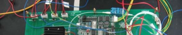

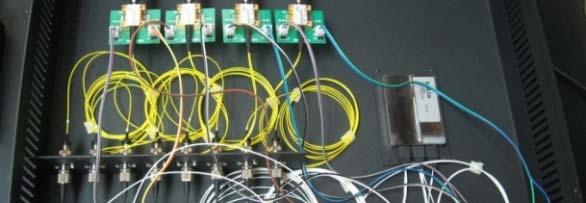
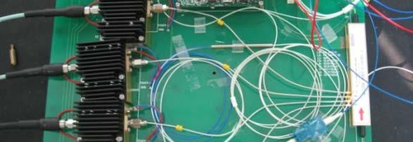
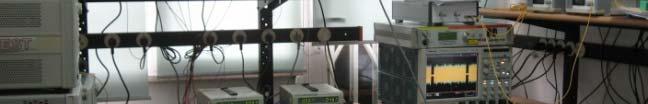
15 Coherent optical communication i is basic technology for 100Gbit/s speed Drawbacks: Expensive, Separate device Large size Low efficient SKL lab Advanced Optical Communication Systems and Networks, 17


16 Si-based monolithic photonic integrated 100Gb/s coherent receivers Device: Coupler PBS Hybrids Detector Modulator 18
17 100G optical receiver 100 Gb/s coherent receiver High bandwidth (>20GHz) High responsively (0.6 A/W) Low dark current (hundreds of na) 19


18 III-V group photodetectors: Absorption coefficients for Ge, Si and (In)GaAs not CMOS compatible complicated fabrication very expensive Germanium photodetectors: compatible with the CMOS process high responsivity low cost 20 20
19 (a) 3D schematic structure of the Ge pin waveguide photodetector integrated on top of an SOI waveguide. (b) Schematic cross-sectional view of the photodetector. The light is evanescently coupled to the overlying Germanium layer
20 Ge Si Ge SiO 2 The field distribution of the photodetector by beam propagation simulation. Almost 95% of the light power is absorbed when the Germanium length reaches about 8 μm. The photodetector is designed to be μm 2. 23


21 (a) (b) (a)the top view SEM image of the rib waveguide and the Si pedestal. (b)the top view SEM image of the μm 2 photodetector after all processing. The combined SiGe buffer layer with the two step growth approach. The final thickness of the Germanium layer was 500nm
22 Dark current (a) (b) A low dark current of 0.66μA at the bias of -1V is achieved. The longer the PD, the larger dark current
23 The germanium photodetector exhibited a high 3-dB bandwidth of 22GHz at the wavelength of 1.55μm. A clear open eye diagram at 30Gb/s was also obtained 27
24 衷心感谢台大的老师和同学们!!! 欢迎你们明年去北大访问!!! 希望 2014 年到台大交流 也希望能有研究生交流 Taibei, 26 Dec,
Photodiode: LECTURE-5
 LECTURE-5 Photodiode: Photodiode consists of an intrinsic semiconductor sandwiched between two heavily doped p-type and n-type semiconductors as shown in Fig. 3.2.2. Sufficient reverse voltage is applied
Optical Receivers Theory and Operation
 Optical Receivers Theory and Operation Photo Detectors Optical receivers convert optical signal (light) to electrical signal (current/voltage) Hence referred O/E Converter Photodetector is the fundamental
High-speed Ge photodetector monolithically integrated with large cross silicon-on-insulator waveguide
 [ APPLIED PHYSICS LETTERS ] High-speed Ge photodetector monolithically integrated with large cross silicon-on-insulator waveguide Dazeng Feng, Shirong Liao, Roshanak Shafiiha. etc Contents 1. Introduction
Lecture 9 External Modulators and Detectors
 Optical Fibres and Telecommunications Lecture 9 External Modulators and Detectors Introduction Where are we? A look at some real laser diodes. External modulators Mach-Zender Electro-absorption modulators
Optical Fiber Communication Lecture 11 Detectors
 Optical Fiber Communication Lecture 11 Detectors Warriors of the Net Detector Technologies MSM (Metal Semiconductor Metal) PIN Layer Structure Semiinsulating GaAs Contact InGaAsP p 5x10 18 Absorption InGaAs
Lecture 18: Photodetectors
 Lecture 18: Photodetectors Contents 1 Introduction 1 2 Photodetector principle 2 3 Photoconductor 4 4 Photodiodes 6 4.1 Heterojunction photodiode.................... 8 4.2 Metal-semiconductor photodiode................
OFCS OPTICAL DETECTORS 11/9/2014 LECTURES 1
 OFCS OPTICAL DETECTORS 11/9/2014 LECTURES 1 1-Defintion & Mechanisms of photodetection It is a device that converts the incident light into electrical current External photoelectric effect: Electrons are
Detectors for Optical Communications
 Optical Communications: Circuits, Systems and Devices Chapter 3: Optical Devices for Optical Communications lecturer: Dr. Ali Fotowat Ahmady Sep 2012 Sharif University of Technology 1 Photo All detectors
OPTOELECTRONIC and PHOTOVOLTAIC DEVICES
 OPTOELECTRONIC and PHOTOVOLTAIC DEVICES Outline 1. Introduction to the (semiconductor) physics: energy bands, charge carriers, semiconductors, p-n junction, materials, etc. 2. Light emitting diodes Light
Electronic-Photonic ICs for Low Cost and Scalable Datacenter Solutions
 Electronic-Photonic ICs for Low Cost and Scalable Datacenter Solutions Christoph Theiss, Director Packaging Christoph.Theiss@sicoya.com 1 SEMICON Europe 2016, October 27 2016 Sicoya Overview Spin-off from
Silicon Photonics Photo-Detector Announcement. Mario Paniccia Intel Fellow Director, Photonics Technology Lab
 Silicon Photonics Photo-Detector Announcement Mario Paniccia Intel Fellow Director, Photonics Technology Lab Agenda Intel s Silicon Photonics Research 40G Modulator Recap 40G Photodetector Announcement
Optical Amplifiers. Continued. Photonic Network By Dr. M H Zaidi
 Optical Amplifiers Continued EDFA Multi Stage Designs 1st Active Stage Co-pumped 2nd Active Stage Counter-pumped Input Signal Er 3+ Doped Fiber Er 3+ Doped Fiber Output Signal Optical Isolator Optical
Avalanche Photodiode. Instructor: Prof. Dietmar Knipp Presentation by Peter Egyinam. 4/19/2005 Photonics and Optical communicaton
 Avalanche Photodiode Instructor: Prof. Dietmar Knipp Presentation by Peter Egyinam 1 Outline Background of Photodiodes General Purpose of Photodiodes Basic operation of p-n, p-i-n and avalanche photodiodes
Chapter 3 OPTICAL SOURCES AND DETECTORS
 Chapter 3 OPTICAL SOURCES AND DETECTORS 3. Optical sources and Detectors 3.1 Introduction: The success of light wave communications and optical fiber sensors is due to the result of two technological breakthroughs.
New advances in silicon photonics Delphine Marris-Morini
 New advances in silicon photonics Delphine Marris-Morini P. Brindel Alcatel-Lucent Bell Lab, Nozay, France New Advances in silicon photonics D. Marris-Morini, L. Virot*, D. Perez-Galacho, X. Le Roux, D.
Physics of Waveguide Photodetectors with Integrated Amplification
 Physics of Waveguide Photodetectors with Integrated Amplification J. Piprek, D. Lasaosa, D. Pasquariello, and J. E. Bowers Electrical and Computer Engineering Department University of California, Santa
A silicon avalanche photodetector fabricated with standard CMOS technology with over 1 THz gain-bandwidth product
 A silicon avalanche photodetector fabricated with standard CMOS technology with over 1 THz gain-bandwidth product Myung-Jae Lee and Woo-Young Choi* Department of Electrical and Electronic Engineering,
Optical Communications
 Optical Communications Telecommunication Engineering School of Engineering University of Rome La Sapienza Rome, Italy 2005-2006 Lecture #4, May 9 2006 Receivers OVERVIEW Photodetector types: Photodiodes
Heinrich-Hertz-Institut Berlin
 NOVEMBER 24-26, ECOLE POLYTECHNIQUE, PALAISEAU OPTICAL COUPLING OF SOI WAVEGUIDES AND III-V PHOTODETECTORS Ludwig Moerl Heinrich-Hertz-Institut Berlin Photonic Components Dept. Institute for Telecommunications,,
Ultra-sensitive SiGe Bipolar Phototransistors for Optical Interconnects
 Ultra-sensitive SiGe Bipolar Phototransistors for Optical Interconnects Michael Roe Electrical Engineering and Computer Sciences University of California at Berkeley Technical Report No. UCB/EECS-2012-123
14.2 Photodiodes 411
 14.2 Photodiodes 411 Maximum reverse voltage is specified for Ge and Si photodiodes and photoconductive cells. Exceeding this voltage can cause the breakdown and severe deterioration of the sensor s performance.
Opto-electronic Receivers
 Purpose of a Receiver The receiver fulfils the function of optoelectronic conversion of an input optical signal into an output electrical signal (data stream). The purpose is to recover the data transmitted
Lecture: Integration of silicon photonics with electronics. Prepared by Jean-Marc FEDELI CEA-LETI
 Lecture: Integration of silicon photonics with electronics Prepared by Jean-Marc FEDELI CEA-LETI Context The goal is to give optical functionalities to electronics integrated circuit (EIC) The objectives
InP-based Waveguide Photodetector with Integrated Photon Multiplication
 InP-based Waveguide Photodetector with Integrated Photon Multiplication D.Pasquariello,J.Piprek,D.Lasaosa,andJ.E.Bowers Electrical and Computer Engineering Department University of California, Santa Barbara,
Fundamentals of CMOS Image Sensors
 CHAPTER 2 Fundamentals of CMOS Image Sensors Mixed-Signal IC Design for Image Sensor 2-1 Outline Photoelectric Effect Photodetectors CMOS Image Sensor(CIS) Array Architecture CIS Peripherals Design Considerations
FIBER OPTICS. Prof. R.K. Shevgaonkar. Department of Electrical Engineering. Indian Institute of Technology, Bombay. Lecture: 20
 FIBER OPTICS Prof. R.K. Shevgaonkar Department of Electrical Engineering Indian Institute of Technology, Bombay Lecture: 20 Photo-Detectors and Detector Noise Fiber Optics, Prof. R.K. Shevgaonkar, Dept.
Chap14. Photodiode Detectors
 Chap14. Photodiode Detectors Mohammad Ali Mansouri-Birjandi mansouri@ece.usb.ac.ir mamansouri@yahoo.com Faculty of Electrical and Computer Engineering University of Sistan and Baluchestan (USB) Design
NON-AMPLIFIED PHOTODETECTOR USER S GUIDE
 NON-AMPLIFIED PHOTODETECTOR USER S GUIDE Thank you for purchasing your Non-amplified Photodetector. This user s guide will help answer any questions you may have regarding the safe use and optimal operation
Figure Responsivity (A/W) Figure E E-09.
 Figure E E-09.") OSI Optoelectronics, is a leading manufacturer of fiber optic components for communication systems. The products offer range for Silicon, GaAs and InGaAs to full turnkey solutions. Photodiodes are semiconductor
OSI Optoelectronics, is a leading manufacturer of fiber optic components for communication systems. The products offer range for Silicon, GaAs and InGaAs to full turnkey solutions. Photodiodes are semiconductor
Lecture 4 Fiber Optical Communication Lecture 4, Slide 1
 Lecture 4 Optical transmitters Photon processes in light matter interaction Lasers Lasing conditions The rate equations CW operation Modulation response Noise Light emitting diodes (LED) Power Modulation
Silicon Avalanche Photodetectors Fabricated With Standard CMOS/BiCMOS Technology Myung-Jae Lee
 Silicon Avalanche Photodetectors Fabricated With Standard CMOS/BiCMOS Technology Myung-Jae Lee The Graduate School Yonsei University Department of Electrical and Electronic Engineering Silicon Avalanche
UNIT III. By Ajay Kumar Gautam Asst. Prof. Electronics & Communication Engineering Dev Bhoomi Institute of Technology & Engineering, Dehradun
 UNIT III By Ajay Kumar Gautam Asst. Prof. Electronics & Communication Engineering Dev Bhoomi Institute of Technology & Engineering, Dehradun SYLLABUS Optical Absorption in semiconductors, Types of Photo
Investigate the characteristics of PIN Photodiodes and understand the usage of the Lightwave Analyzer component.
 PIN Photodiode 1 OBJECTIVE Investigate the characteristics of PIN Photodiodes and understand the usage of the Lightwave Analyzer component. 2 PRE-LAB In a similar way photons can be generated in a semiconductor,
Figure Figure E E-09. Dark Current (A) 1.
 1.") OSI Optoelectronics, is a leading manufacturer of fiber optic components for communication systems. The products offer range for Silicon, GaAs and InGaAs to full turnkey solutions. Photodiodes are semiconductor
OSI Optoelectronics, is a leading manufacturer of fiber optic components for communication systems. The products offer range for Silicon, GaAs and InGaAs to full turnkey solutions. Photodiodes are semiconductor
A 3.9 ns 8.9 mw 4 4 Silicon Photonic Switch Hybrid-Integrated with CMOS Driver
 A 3.9 ns 8.9 mw 4 4 Silicon Photonic Switch Hybrid-Integrated with CMOS Driver A. Rylyakov, C. Schow, B. Lee, W. Green, J. Van Campenhout, M. Yang, F. Doany, S. Assefa, C. Jahnes, J. Kash, Y. Vlasov IBM
NON-AMPLIFIED HIGH SPEED PHOTODETECTOR USER S GUIDE
 NON-AMPLIFIED HIGH SPEED PHOTODETECTOR USER S GUIDE Thank you for purchasing your Non-amplified High Speed Photodetector. This user s guide will help answer any questions you may have regarding the safe
Simulation of High Resistivity (CMOS) Pixels
 Pixels") Simulation of High Resistivity (CMOS) Pixels Stefan Lauxtermann, Kadri Vural Sensor Creations Inc. AIDA-2020 CMOS Simulation Workshop May 13 th 2016 OUTLINE 1. Definition of High Resistivity Pixel Also
Simulation of High Resistivity (CMOS) Pixels Stefan Lauxtermann, Kadri Vural Sensor Creations Inc. AIDA-2020 CMOS Simulation Workshop May 13 th 2016 OUTLINE 1. Definition of High Resistivity Pixel Also
Segmented waveguide photodetector with 90% quantum efficiency
 Vol. 26, No. 10 14 May 2018 OPTICS EXPRESS 12499 Segmented waveguide photodetector with 90% quantum efficiency QIANHUAN YU, KEYE SUN, QINGLONG LI, AND ANDREAS BELING* Department of Electrical and Computer
IEEE JOURNAL OF SELECTED TOPICS IN QUANTUM ELECTRONICS 2010 Silicon Photonic Circuits: On-CMOS Integration, Fiber Optical Coupling, and Packaging
 IEEE JOURNAL OF SELECTED TOPICS IN QUANTUM ELECTRONICS 2010 Silicon Photonic Circuits: On-CMOS Integration, Fiber Optical Coupling, and Packaging Christophe Kopp, St ephane Bernab e, Badhise Ben Bakir,
InP-based Waveguide Photodetector with Integrated Photon Multiplication
 InP-based Waveguide Photodetector with Integrated Photon Multiplication D.Pasquariello,J.Piprek,D.Lasaosa,andJ.E.Bowers Electrical and Computer Engineering Department University of California, Santa Barbara,
Silicon sensors for radiant signals. D.Sc. Mikko A. Juntunen
 Silicon sensors for radiant signals D.Sc. Mikko A. Juntunen 2017 01 16 Today s outline Introduction Basic physical principles PN junction revisited Applications Light Ionizing radiation X-Ray sensors in
Photonics and Optical Communication Spring 2005
 Photonics and Optical Communication Spring 2005 Final Exam Instructor: Dr. Dietmar Knipp, Assistant Professor of Electrical Engineering Name: Mat. -Nr.: Guidelines: Duration of the Final Exam: 2 hour You
Examination Optoelectronic Communication Technology. April 11, Name: Student ID number: OCT1 1: OCT 2: OCT 3: OCT 4: Total: Grade:
 Examination Optoelectronic Communication Technology April, 26 Name: Student ID number: OCT : OCT 2: OCT 3: OCT 4: Total: Grade: Declaration of Consent I hereby agree to have my exam results published on
Si and InP Integration in the HELIOS project
 Si and InP Integration in the HELIOS project J.M. Fedeli CEA-LETI, Grenoble ( France) ECOC 2009 1 Basic information about HELIOS HELIOS photonics ELectronics functional Integration on CMOS www.helios-project.eu
Equivalent circuit modeling of InP/InGaAs Heterojunction Phototransistor for application of Radio-on-fiber systems
 Equivalent circuit modeling of InP/InGaAs Heterojunction Phototransistor for application of Radio-on-fiber systems Jae-Young Kim The Graduate School Yonsei University Department of Electrical and Electronic
Lecture 4 INTEGRATED PHOTONICS
 Lecture 4 INTEGRATED PHOTONICS What is photonics? Photonic applications use the photon in the same way that electronic applications use the electron. Devices that run on light have a number of advantages
Si CMOS Technical Working Group
 Si CMOS Technical Working Group CTR, Spring 2008 meeting Markets Interconnects TWG Breakouts Reception TWG reports Si CMOS: photonic integration E-P synergy - Integration - Standardization - Cross-market
Design and Simulation of N-Substrate Reverse Type Ingaasp/Inp Avalanche Photodiode
 International Refereed Journal of Engineering and Science (IRJES) ISSN (Online) 2319-183X, (Print) 2319-1821 Volume 2, Issue 8 (August 2013), PP.34-39 Design and Simulation of N-Substrate Reverse Type
CMOS Phototransistors for Deep Penetrating Light
 CMOS Phototransistors for Deep Penetrating Light P. Kostov, W. Gaberl, H. Zimmermann Institute of Electrodynamics, Microwave and Circuit Engineering, Vienna University of Technology Gusshausstr. 25/354,
InGaAs Avalanche Photodiode. IAG-Series
 InGaAs Avalanche Photodiode IAG-Series DESCRIPTION The IAG-series avalanche photodiode is the largest commercially available InGaAs APD with high responsivity and extremely fast rise and fall times throughout
Comparative Study of an Optical Link with PIN and APD as Photo-Detector Preetam Jain 1, Dr Lochan Jolly 2
 Comparative Study of an Optical Link with PIN and APD as Photo-Detector Preetam Jain 1, Dr Lochan Jolly 2 1 ME EXTC Student Thakur College of Engineering and Technology 2 Professor Thakur College of Engineering
The Past, Present, and Future of Silicon Photonics
 The Past, Present, and Future of Silicon Photonics Myung-Jae Lee High-Speed Circuits & Systems Lab. Dept. of Electrical and Electronic Engineering Yonsei University Outline Introduction A glance at history
Engineering Medical Optics BME136/251 Winter 2018
 Engineering Medical Optics BME136/251 Winter 2018 Monday/Wednesday 2:00-3:20 p.m. Beckman Laser Institute Library, MSTB 214 (lab) *1/17 UPDATE Wednesday, 1/17 Optics and Photonic Devices III: homework
Integration of Optoelectronic and RF Devices for Applications in Optical Interconnect and Wireless Communication
 Integration of Optoelectronic and RF Devices for Applications in Optical Interconnect and Wireless Communication Zhaoran (Rena) Huang Assistant Professor Department of Electrical, Computer and System Engineering
Study and Measurement of the Main Parameters of a Laser quadrant Detector
 Cairo University National Institute of Laser Enhanced Sciences Laser Sciences and Interactions Study and Measurement of the Main Parameters of a Laser quadrant Detector By Eng. Mohamed Abd-Elfattah Abd-Elazim
Measure the roll-off frequency of an acousto-optic modulator
 Slide 1 Goals of the Lab: Get to know some of the properties of pin photodiodes Measure the roll-off frequency of an acousto-optic modulator Measure the cut-off frequency of a pin photodiode as a function
Lecture 6 Fiber Optical Communication Lecture 6, Slide 1
 Lecture 6 Optical transmitters Photon processes in light matter interaction Lasers Lasing conditions The rate equations CW operation Modulation response Noise Light emitting diodes (LED) Power Modulation
OPTI510R: Photonics. Khanh Kieu College of Optical Sciences, University of Arizona Meinel building R.626
 OPTI510R: Photonics Khanh Kieu College of Optical Sciences, University of Arizona kkieu@optics.arizona.edu Meinel building R.626 Photodetectors Introduction Most important characteristics Photodetector
Silicon Photonics Technology Platform To Advance The Development Of Optical Interconnects
 Silicon Photonics Technology Platform To Advance The Development Of Optical Interconnects By Mieke Van Bavel, science editor, imec, Belgium; Joris Van Campenhout, imec, Belgium; Wim Bogaerts, imec s associated
Dynamics of Charge Carriers in Silicon Nanowire Photoconductors Revealed by Photo Hall. Effect Measurements. (Supporting Information)
") Dynamics of Charge Carriers in Silicon Nanowire Photoconductors Revealed by Photo Hall Effect Measurements (Supporting Information) Kaixiang Chen 1, Xiaolong Zhao 2, Abdelmadjid Mesli 3, Yongning He 2*
Dynamics of Charge Carriers in Silicon Nanowire Photoconductors Revealed by Photo Hall Effect Measurements (Supporting Information) Kaixiang Chen 1, Xiaolong Zhao 2, Abdelmadjid Mesli 3, Yongning He 2*
LEDs, Photodetectors and Solar Cells
 LEDs, Photodetectors and Solar Cells Chapter 7 (Parker) ELEC 424 John Peeples Why the Interest in Photons? Answer: Momentum and Radiation High electrical current density destroys minute polysilicon and
UV/EUV CONTINUOUS POSITION SENSOR
 UV/EUV CONTINUOUS POSITION SENSOR ODD-SXUV-DLPSD FEATURES Submicron position resolution Stable response after exposure to UV/EUV 5 mm x 5 mm active area TO-8 windowless package RoHS ELECTRO-OPTICAL CHARACTERISTICS
A Fully Integrated 20 Gb/s Optoelectronic Transceiver Implemented in a Standard
 A Fully Integrated 20 Gb/s Optoelectronic Transceiver Implemented in a Standard 0.13 µm CMOS SOI Technology School of Electrical and Electronic Engineering Yonsei University 이슬아 1. Introduction 2. Architecture
CMOS-Compatible High-Speed Silicon Photodetectors for Gbps Fiber-Fed Wireline/Wireless Communication Systems
 CMOS-Compatible High-Speed Silicon Photodetectors for Gbps Fiber-Fed Wireline/Wireless Communication Systems Hyo-Soon Kang THE GRADUATE SCHOOL YONSEI UNIVERSITY Department of Electrical and Electronic
Low threshold continuous wave Raman silicon laser
 NATURE PHOTONICS, VOL. 1, APRIL, 2007 Low threshold continuous wave Raman silicon laser HAISHENG RONG 1 *, SHENGBO XU 1, YING-HAO KUO 1, VANESSA SIH 1, ODED COHEN 2, OMRI RADAY 2 AND MARIO PANICCIA 1 1:
MOSFET short channel effects
 MOSFET short channel effects overview Five different short channel effects can be distinguished: velocity saturation drain induced barrier lowering (DIBL) impact ionization surface scattering hot electrons
GPD. Germanium Photodetectors. GPD Optoelectronics Corp. OPTOELECTRONICS CORP. Small & Large Area pn, pin detectors Two-color detectors
 GPD Small & Large Area pn, pin detectors Two-color detectors OPTOELECTRONICS CORP. Germanium Photodetectors Large and Small Area Wide Performance Range TE Coolers and Dewars Available Filtered Windows
Optical Sources and Detectors
 Optical Sources and Detectors 1. Optical Sources Optical transmitter coverts electrical input signal into corresponding optical signal. The optical signal is then launched into the fiber. Optical source
Optodevice Data Book ODE I. Rev.9 Mar Opnext Japan, Inc.
 Optodevice Data Book ODE-408-001I Rev.9 Mar. 2003 Opnext Japan, Inc. Section 1 Operating Principles 1.1 Operating Principles of Laser Diodes (LDs) and Infrared Emitting Diodes (IREDs) 1.1.1 Emitting Principles
HIGH-EFFICIENCY MQW ELECTROABSORPTION MODULATORS
 HIGH-EFFICIENCY MQW ELECTROABSORPTION MODULATORS J. Piprek, Y.-J. Chiu, S.-Z. Zhang (1), J. E. Bowers, C. Prott (2), and H. Hillmer (2) University of California, ECE Department, Santa Barbara, CA 93106
HIGH SPEED FIBER PHOTODETECTOR USER S GUIDE
 HIGH SPEED FIBER PHOTODETECTOR USER S GUIDE Thank you for purchasing your High Speed Fiber Photodetector. This user s guide will help answer any questions you may have regarding the safe use and optimal
What is the highest efficiency Solar Cell?
 What is the highest efficiency Solar Cell? GT CRC Roof-Mounted PV System Largest single PV structure at the time of it s construction for the 1996 Olympic games Produced more than 1 billion watt hrs. of
Recent Development and Study of Silicon Solid State Photomultiplier (MRS Avalanche Photodetector)
") Recent Development and Study of Silicon Solid State Photomultiplier (MRS Avalanche Photodetector) Valeri Saveliev University of Obninsk, Russia Vienna Conference on Instrumentation Vienna, 20 February
Recent Development and Study of Silicon Solid State Photomultiplier (MRS Avalanche Photodetector) Valeri Saveliev University of Obninsk, Russia Vienna Conference on Instrumentation Vienna, 20 February
MAHALAKSHMI ENGINEERING COLLEGE TIRUCHIRAPALLI
 MAHALAKSHMI ENGINEERING COLLEGE TIRUCHIRAPALLI - 621213 DEPARTMENT : ECE SUBJECT NAME : OPTICAL COMMUNICATION & NETWORKS SUBJECT CODE : EC 2402 UNIT III: SOURCES AND DETECTORS PART -A (2 Marks) 1. What
SNR characteristics of 850-nm OEIC receiver with a silicon avalanche photodetector
 SNR characteristics of 850-nm OEIC receiver with a silicon avalanche photodetector Jin-Sung Youn, 1 Myung-Jae Lee, 1 Kang-Yeob Park, 1 Holger Rücker, 2 and Woo-Young Choi 1,* 1 Department of Electrical
High Speed pin Photodetector with Ultra-Wide Spectral Responses
 High Speed pin Photodetector with Ultra-Wide Spectral Responses C. Tam, C-J Chiang, M. Cao, M. Chen, M. Wong, A. Vazquez, J. Poon, K. Aihara, A. Chen, J. Frei, C. D. Johns, Ibrahim Kimukin, Achyut K. Dutta
High speed silicon-based optoelectronic devices Delphine Marris-Morini Institut d Electronique Fondamentale, Université Paris Sud
 High speed silicon-based optoelectronic devices Delphine Marris-Morini Institut d Electronique Fondamentale, Université Paris Sud Data centers Optical telecommunications Environment Interconnects Silicon
EXAMINATION FOR THE DEGREE OF B.E. and M.E. Semester
 EXAMINATION FOR THE DEGREE OF B.E. and M.E. Semester 2 2009 101908 OPTICAL COMMUNICATION ENGINEERING (Elec Eng 4041) 105302 SPECIAL STUDIES IN MARINE ENGINEERING (Elec Eng 7072) Official Reading Time:
Development of the Pixelated Photon Detector. Using Silicon on Insulator Technology. for TOF-PET
 July 24, 2015 Development of the Pixelated Photon Detector Using Silicon on Insulator Technology for TOF-PET A.Koyama 1, K.Shimazoe 1, H.Takahashi 1, T. Orita 2, Y.Arai 3, I.Kurachi 3, T.Miyoshi 3, D.Nio
Fabrication of antenna integrated UTC-PDs as THz sources
 Invited paper Fabrication of antenna integrated UTC-PDs as THz sources Siwei Sun 1, Tengyun Wang, Xiao xie 1, Lichen Zhang 1, Yuan Yao and Song Liang 1* 1 Key Laboratory of Semiconductor Materials Science,
Amplified Photodetectors
 Amplified Photodetectors User Guide (800)697-6782 sales@eotech.com www.eotech.com Page 1 of 6 EOT AMPLIFIED PHOTODETECTOR USER S GUIDE Thank you for purchasing your Amplified Photodetector from EOT. This
LED lecture. Wei Chih Wang University of Washington
 LED lecture Wei Chih Wang University of Washington Linear and Nonlinear electronics current voltage Vaccum tube (i.e. type 2A3) voltage Thermistor (large negative temperature coefficient of resistivity)
Solar Cell Parameters and Equivalent Circuit
 9 Solar Cell Parameters and Equivalent Circuit 9.1 External solar cell parameters The main parameters that are used to characterise the performance of solar cells are the peak power P max, the short-circuit
Fabrication of High-Speed Resonant Cavity Enhanced Schottky Photodiodes
 Fabrication of High-Speed Resonant Cavity Enhanced Schottky Photodiodes Abstract We report the fabrication and testing of a GaAs-based high-speed resonant cavity enhanced (RCE) Schottky photodiode. The
EE 230: Optical Fiber Communication Transmitters
 EE 230: Optical Fiber Communication Transmitters From the movie Warriors of the Net Laser Diode Structures Most require multiple growth steps Thermal cycling is problematic for electronic devices Fabry
Semiconductor Optical Active Devices for Photonic Networks
 UDC 621.375.8:621.38:621.391.6 Semiconductor Optical Active Devices for Photonic Networks VKiyohide Wakao VHaruhisa Soda VYuji Kotaki (Manuscript received January 28, 1999) This paper describes recent
Lecture 14: Photodiodes
 Lecture 14: Photodiodes Background concepts p-n photodiodes photoconductive/photovoltaic modes p-i-n photodiodes responsivity and bandwidth Reading: Senior 8.1-8.8.3 Keiser Chapter 6 1 Electron-hole photogeneration
DOCTORAL DISSERTATION CHARACTERIZATION AND OPTIMIZATION OF AVALANCHE PHOTODIODES FABRICATED BY STANDARD CMOS PROCESS FOR HIGH-SPEED PHOTORECEIVERS
 DOCTORAL DISSERTATION CHARACTERIZATION AND OPTIMIZATION OF AVALANCHE PHOTODIODES FABRICATED BY STANDARD CMOS PROCESS FOR HIGH-SPEED PHOTORECEIVERS 高速光レシーバの実現に向けた CMOS アバランシェ光検出器の特性評価と最適化 Optical and Electronic
Silicon Photonics in Optical Communications. Lars Zimmermann, IHP, Frankfurt (Oder), Germany
, Germany") Silicon Photonics in Optical Communications Lars Zimmermann, IHP, Frankfurt (Oder), Germany Outline IHP who we are Silicon photonics Photonic-electronic integration IHP photonic technology Conclusions
Silicon Photonics in Optical Communications Lars Zimmermann, IHP, Frankfurt (Oder), Germany Outline IHP who we are Silicon photonics Photonic-electronic integration IHP photonic technology Conclusions
h v [ME08] Development of silicon planar P-I-N photodiode P Susthitha Menon a/p N V Visvanathan, Sahbudin Shaari
![h v [ME08] Development of silicon planar P-I-N photodiode P Susthitha Menon a/p N V Visvanathan, Sahbudin Shaari](/thumbs/73/69295145.jpg "h v [ME08] Development of silicon planar P-I-N photodiode P Susthitha Menon a/p N V Visvanathan, Sahbudin Shaari") [ME08] Development of silicon planar P-I-N photodiode P Susthitha Menon a/p N V Visvanathan, Sahbudin Shaari Photonics Technology Laboratory (PTL), Institute of Micro Engineering and Nanoelectronics (IMEN),
[ME08] Development of silicon planar P-I-N photodiode P Susthitha Menon a/p N V Visvanathan, Sahbudin Shaari Photonics Technology Laboratory (PTL), Institute of Micro Engineering and Nanoelectronics (IMEN),
Resonant normal-incidence separate-absorptioncharge-multiplication. photodiodes
 Resonant normal-incidence separate-absorptioncharge-multiplication Ge/Si avalanche photodiodes Daoxin Dai 1*, Hui-Wen Chen 1, John E. Bowers 1 Yimin Kang 2, Mike Morse 2, Mario J. Paniccia 2 1 University
Vertical p-i-n germanium photodetector with high external responsivity integrated with large core Si waveguides
 Vertical p-i-n germanium photodetector with high external responsivity integrated with large core Si waveguides Ning-Ning Feng* 1, Po Dong 1, Dawei Zheng 1, Shirong Liao 1, Hong Liang 1, Roshanak Shafiiha
Optical Fibre Communication Systems
 Optical Fibre Communication Systems Lecture 4 - Detectors & Receivers Professor Z Ghassemlooy Northumbria Communications Laboratory Faculty of Engineering and Environment The University of Northumbria
Research Article Responsivity Enhanced NMOSFET Photodetector Fabricated by Standard CMOS Technology
 Advances in Condensed Matter Physics Volume 2015, Article ID 639769, 5 pages http://dx.doi.org/10.1155/2015/639769 Research Article Responsivity Enhanced NMOSFET Photodetector Fabricated by Standard CMOS
Review of Semiconductor Physics
 Review of Semiconductor Physics k B 1.38 u 10 23 JK -1 a) Energy level diagrams showing the excitation of an electron from the valence band to the conduction band. The resultant free electron can freely
Photodiode Characteristics and Applications
 Photodiode Characteristics and Applications Silicon photodiodes are semiconductor devices responsive to highenergy particles and photons. Photodiodes operate by absorption of photons or charged particles
Compact two-mode (de)multiplexer based on symmetric Y-junction and Multimode interference waveguides
multiplexer based on symmetric Y-junction and Multimode interference waveguides") Compact two-mode (de)multiplexer based on symmetric Y-junction and Multimode interference waveguides Yaming Li, Chong Li, Chuanbo Li, Buwen Cheng, * and Chunlai Xue State Key Laboratory on Integrated Optoelectronics,
Compact two-mode (de)multiplexer based on symmetric Y-junction and Multimode interference waveguides Yaming Li, Chong Li, Chuanbo Li, Buwen Cheng, * and Chunlai Xue State Key Laboratory on Integrated Optoelectronics,
Chapter 1: Semiconductor Diodes
 Chapter 1: Semiconductor Diodes Diodes The diode is a 2-terminal device. A diode ideally conducts in only one direction. 2 Diode Characteristics Conduction Region Non-Conduction Region The voltage across
Non-amplified Photodetectors
 Non-amplified Photodetectors User Guide (800)697-6782 sales@eotech.com www.eotech.com Page 1 of 9 EOT NON-AMPLIFIED PHOTODETECTOR USER S GUIDE Thank you for purchasing your Non-amplified Photodetector
Optical 90 Hybrids Based on Silicon-on-Insulator. Multimode Interference Couplers
 Optical 90 Hybrids Based on Silicon-on-Insulator Multimode Interference Couplers Tingting Hong, Wei Yang, Huaxiang Yi, Xingjun Wang *, Yanping Li *, Ziyu Wang, Zhiping Zhou State Key Laboratory of Advanced