OPTI510R: Photonics. Khanh Kieu College of Optical Sciences, University of Arizona Meinel building R.626
|
|
|
- Georgiana Logan
- 6 years ago
- Views:
Transcription
1 OPTI510R: Photonics Khanh Kieu College of Optical Sciences, University of Arizona Meinel building R.626
2 Announcement Homework #6 is due today Final exam May 2, room 307, starting at 11 AM
3 Review Introduction to optical fibers Attenuation and dispersion Fiber fabrication Dispersion compensation Nonlinear optical effects Optical amplifiers Passive fiber components Introduction to lasers Semiconductor lasers Detectors Semiconductor detectors Optical network
4 Goals Understand the most important concepts in Photonics Learn the working principles of photonics devices Identify the remaining challenges in the field Think about possible solutions

5 Introduction to optical fibers

6 Optical fibers The working principle of standard optical fiber can be explained using TIR Photonics crystal fibers Standard fiber PCF HC-PCF The refractive index of the core is smaller than the refractive index of the cladding J. C. Knight, Photonic crystal fibers, Nature 424, (2003)
7 Guided-wave analysis n 2 core for < a a n 1 cladding for > a
8 Guided-wave analysis (credit: G. Agrawal)
9 Guided-wave analysis (credit: G. Agrawal)
10 Guided-wave analysis (credit: G. Agrawal)
11 Bessel function basics Bessel functions of the first kind Modified Bessel functions of the second kind u( r) J ( k r) l (core) T u(r) = K l (gr) (cladding)
12 Eigen-value equation (credit: G. Agrawal)
13 Eigen-value equation (credit: G. Agrawal)
")
14 Eigen-value equation (credit: G. Agrawal)
15 Attenuation in optical fiber Attenuation coefficient (db/km) a = 1 L 10log 10 1 T with T = P(L) P(0) Power transmission ratio as a function of distance z P( z) P(0) e - z for in km -1 Calculate (db) through (km -1 ) (db) = 4.343* (km -1 )
16 Sources of attenuation in silica fiber Absorption Vibrational transitions in the IR Electronic and molecular transitions in the UV Extrinsic absorption from adsorbed water and other impurities Scattering Rayleigh scattering Extrinsic scattering from defects due to manufacturing errors Raman, Brillouin scattering
17 Propagation loss in optical fiber Current loss is < 0.2dB/km for single mode fiber working around 1550nm
18 Communication window <1dB/mile of loss over >10 THz of bandwidth! Loss performance in fused silica fiber
19 Dispersion in optical fiber Modal dispersion Occurs in multimode fibers coming from differences in group velocity for different modes Material dispersion Results from the wavelength dependence of the bulk refractive index Waveguide dispersion Results from the wavelength dependence of the effective index in a waveguide Material + waveguide dispersion is termed chromatic dispersion Polarization mode dispersion Results from the fact that different polarizations travel at different speeds due to small birefringence that is present Nonlinear dispersion example is self-phase modulation

20 Modal dispersion Modal dispersion occurs in multimode fibers as a result of differences in the group velocities of the various modes. A single pulse of light entering an M-mode fiber spreads into M pulses. Estimate of pulse spread Where v min and v max are the smallest and largest group velocity of the modes. For step index fiber, v 1 2 L v min L v max 2 2 min c1 1 ), vmax c1, ( n1 n2 ) / 2, ( n L 2c 1 2 1
21 Material dispersion Spread of wave packet after traveling a distance L through a dispersive material
22 Waveguide dispersion
23 Waveguide dispersion w : waveguide delay m : material delay Waveguide dispersion!
24 Waveguide dispersion

25 Chromatic dispersion of SMF Chromatic dispersion is the combination of material and waveguide dispersion in single-mode fiber at 1.55 mm, D=+17ps/km-nm GVD at mm, dispersion is zero
26 Fabrication techniques Fiber preform fabrication Fiber pulling


27 Rod-in-tube technique Rod-in-tube method: UA High precision ultrasonic drilling and grinding machines for glass rod processing UA fiber drawing tower


28 Modified Chemical deposition Modified chemical vapor deposition method


29 Active fiber fabrication MCVD process Nano-particle vapor deposition (Liekki)
30 Specialty optical fibers There are a lot of specialty optical fibers! Photonics crystal fibers Doped (active) optical fibers Liquid core optical fibers (if have time) Large mode area optical fibers Chiral core coupled optical fibers Polarizing fibers

31 Photonics crystal fibers Standard fiber PCF HC-PCF a PCF preform J. C. Knight, Photonic crystal fibers, Nature 424, (2003)
32 Dispersion compensation Dispersion compensation Pre-chirp technique Dispersion compensating fibers Chirped fiber Bragg grating
33 Dispersion compensating fibers

34 Dispersion compensating fibers Standard fiber Dispersion compensating fiber Advantage: Fiber format Low cost Broadband Disadvantage: Small mode field diameter Higher loss DCF modules

35 Nonlinear effects in optical fibers Introduction to nonlinear optics Stimulated Brillouin scattering Stimulated Raman scattering Self-phase modulation Cross phase modulation Soliton propagation Four-Wave-Mixing (FWM)
36 Nonlinear optics E Electron (2), (3) are very small R. W. Boyd, Nonlinear Optics, (Academic Press, 2008)
37 Nonlinear optical effects Second harmonic generation (SHG) Third harmonic generation (THG) High harmonic generation (HHG) Sum/Difference frequency generation (SFG/DFG) Optical parametric processes (OPA, OPO, OPG) Kerr effect Self-focusing Self-phase modulation (SPM) Cross-phase modulation (XPM) Four-wave mixing (FWM) Multiphoton absorption Photo-ionization Raman/Brillouin scattering and more
38 Stimulated Brillouin scattering Predicted by Leon Brillouin in 1922 Scattering of light from acoustic waves Becomes a stimulated process when input power exceeds a threshold level Low threshold power for long fibers (5 mw) Most of the power reflected backward after SBS threshold is reached!
39 Stimulated Brillouin scattering Pump produces density variations through electrostriction, resulting in an index grating which generates Stokes wave through Bragg diffraction SBS Energy and momentum conservation require: B = p - s ; k A =k p k s Acoustic waves satisfy the dispersion relation: B = v A * k A = v A * (k p k s ) 2* v A * k p = 2* v A *2 *n p / p f A = B /2 = 2* v A *2 *n p / p ~ 11GHz (Brillouin frequency shift) if we use A = 5.96 km/s, n p = 1.45, and p = 1550nm
40 Brillouin gain spectrum in optical fibers Measured spectra for (a) silica-core (b) depressed-cladding, and (c) dispersion-shifted fibers Brillouin gain spectrum is quite narrow (50 MHz) Brillouin shift depends on GeO 2 doping within the core Multiple peaks are due to the excitation of different acoustic modes G. P. Agrawal, Nonlinear Fiber Optics, (Academic Press, 2007)
")
41 Brillouin threshold in optical fibers is the fiber loss g B is the Brillouin gain coefficient L e is the effective length P th is the Brillouin threshold G. P. Agrawal, Nonlinear Fiber Optics, (Academic Press, 2007)
42 Stimulated Raman scattering Discovered by C. V. Raman in 1928 Scattering of light from vibrating silica molecules Amorphous nature of silica turns vibrational state into a band Raman gain is maximum near 13 THz Scattered light red-shifted by 100 nm in the 1.5 mm region G. P. Agrawal, Nonlinear Fiber Optics, (Academic Press, 2007)
43 SRS threshold For telecom fibers, A eff = µm 2 g R = m/w Threshold power P th 100mW is too large to be of concern Inter-channel crosstalk in WDM systems because of Raman gain
44 Self-phase modulation (SPM) NL =.P 0.L Output spectrum as the function of the nonlinear phase shift First observed inside optical fiber by Stolen and Lin (1978) 90-ps pulses transmitted through a 100-m-long fiber Output spectrum depends on shape and chirp of input pulses. Even spectral compression can occur for suitably chirped pulses
45 Optical Amplifiers Erbium Doped Fiber Amplifiers (EDFAs) Semiconductor Optical Amplifiers Raman Amplifiers Optical Parametric Amplifiers
46 Types of Optical Amplifiers Erbium Doped Fiber Amplifiers (EDFA s) Best performance Low cost, robust Wide spread use Semiconductor Optical Amplifiers Small package Potential use for low-cost applications Potential use for optical switching Raman Amplifiers Better noise performance compared to EDFA Optical parametric amplifier High gain, broader bandwidth
47 Erbium-doped fiber amplifier Working around 1550nm Wide operating bandwidth Amplification of multiple channels Diode pumping Low cost, robust First demonstration Prof. David Payne and team Published the research paper in the year 1987 at the University of Southampton, UK
48 Erbium-doped fiber amplifier Main pump wavelengths: 980nm and 1480nm
49 Main optical characteristics Amplifier gain: G = 10*log (P out /P in ) Gain non-uniformity Gain bandwidth ASE Gain saturation Noise figure:
50 Gain saturation
51 Typical amplifier performance
52 EDFA: Disadvantages Can only work at a narrow wavelength range (C and L band) Requires specially doped fiber as gain medium Three-level system, so gain medium is opaque at signal wavelengths until pumped Requires long path length of gain medium (tens of meters in glass) Gain very wavelength-dependent and must be flattened Gain limited by cooperative quenching Relatively high noise figure due to ASE


53 Semiconductor optical amplifiers Small package Potential use for low-cost applications Potential use for optical switching
54 Semiconductor optical amplifiers Performance of a typical SOA Compared to EDFA: Lower gain, high noise figure, and lower output power
55 Semiconductor optical amplifiers
56 Raman Fiber Amplifiers Working principle of EDFA Schematic of the quantum mechanical process taking place during Raman scattering Raman Amplification in Fiber Optical Communication Systems, edited by Clifford Headley, Govind Agrawal, Elsevier Academic Press 2005
57 Raman Fiber Amplifiers Raman gain profiles for a 1510-nm pump in three different fiber types. SMF, standard single mode fiber; DSF, dispersion shifted fiber; DCF, dispersion compensating fiber
58 Raman Fiber Amplifiers Schematic diagram of a Raman amplifier
59 Raman Fiber Amplifiers Evolution of signal power in a bidirectionally pumped, 100-km-long Raman amplifier as the contribution of forward pumping is varied from 0 to 100% Which one is better? Co-pumping or Counter-pumping?
60 Optical Parametric Amplifier Degenerate and non-degenerate FWM process depicted on an energy level diagram Require optical fiber with zero dispersion near the pump wavelength for phase matching
61 Optical Parametric Amplifier Parametric gains are on both side of the pump laser
62 Optical Parametric Amplifier FOPO with 70dB gain!
63 Optical Parametric Amplifier Advantages: Gain bandwidth increasing with pump power Arbitrary center wavelength Very large gain (70dB) Unidirectional gain (no need for isolator) Compatibility with all-fiber devices High power capability Distributed amplification (low noise figure)
64 Passive fiber components Fiber coupler Variable fiber coupler WDM Isolator Attenuator Modulator Switches Pump/signal combiner Polarization splitter/combiner Collimator Fiber delay line Polarizer Tunable filter Circulator Faraday rotator mirror
65 Passive fiber components Directional couplers WDM couplers Isolators Fiber spicing and connectorization
66 (booster) amplifier transmission fiber dispersion compensation (in-line) amplifier transmission fiber dispersion compensation (pre-) amplifier WDM mux WDM demux EDFA EDFA EDFA 1 2 Point-to-point WDM Transmission System - Building Blocks - transmitter terminal Tx transmission line point-to-point link section span amplifier span receiver terminal Rx SMF or NZDF SMF or NZDF 3 4 DC DC n Raman pump Raman pump n
67 Lasers Brief history Laser characteristics Laser types Laser modes of operation Laser market Fiber lasers

68 Longitudinal modes Allowed modes of the cavity are those where mirror separation is equal to multiple of half wavelength.,q is an integer Frequency separation: for L >> L


69 Laser types Solid state lasers (crystal based) Gas lasers Semiconductor lasers Fiber lasers
70 Modes of operation CW Continuous wave Single-frequency lasers Q-switched lasers Q-switched (ns, us) Mode-locked lasers ML (ps, fs)
71 Semiconductor lasers Brief history p-n junction Semiconductor laser based on p-n junction Double heterostructure Fabrication tools Bandgap engineering Examples of semiconductor lasers
72 Lasers based on p-n junction p + Junction n + E c E v E F p E g Ho les in V B Electro ns ev o Electro ns in C B E F n E c E c E g p + In version reg io n n + E c ev E F n E F p (a) E v (b) The energy band diagram of a degenerately doped p-n with no bias. (b) Band diagram with a sufficiently large forward bias to cause population inversion and hence stimulated emission S.O. Kasap, Optoelectronics (Prentice Hall) V
 Current Cleaved surface mirror p + L L GaAs Electrode n + GaAs Electrode Active region (stimulated")
73 Lasers based on p-n junction January 1962: observations of super-lumenscences in GaAs p-n junctions (Ioffe Institute) Sept.-Dec. 1962: laser action in GaAs and GaAsP p-n junctions (General Electric, IBM, Lebedev Institute) Current Cleaved surface mirror p + L L GaAs Electrode n + GaAs Electrode Active region (stimulated emission region) A schematic illustration of a GaAs homojunction laser diode. The cleaved surfaces act as reflecting mirrors S.O. Kasap, Optoelectronics (Prentice Hall) Light intensity Wavelength
74 Lasers based on heterostructure p-n junction design requires cryogenic temperature to lase Large current density needed to create population inversion Solution: Double Heterostructure! (DHS) (a) (b) Electrons in CB E c E v 2 ev n AlGaAs p GaAs (~0.1 mm) 1.4 ev Holes in VB AlGaAs E c p 2 ev E c E v (a) A double heterostructure diode has two junctions which are between two different bandgap semiconductors (GaAs and AlGaAs). (b) Simplified energy band diagram under a large forward bias. Lasing recombination takes place in the p- GaAs layer, the active layer Refractive index (c) Photon density (d) Active region n ~ 5% (c) Higher bandgap materials have a lower refractive index (d) AlGaAs layers provide lateral optical confinement S.O. Kasap, Optoelectronics (Prentice Hall)
75 Lasers based on heterostructure Two important advantages: 1. Due to the thin p-gaas layer a minimal amount of current is required to increase the concentration of injected carriers at a fast rate. This is how threshold current is reduced for the purpose of population inversion and optical gain. 2. A semiconductor with a wider bandgap (AlGaAs) will also have a lower refractive index than GaAs. This difference in refractive index is what establishes an optical dielectric waveguide that ultimately confines photons to the active region. Room temperature operation possible!
76 Lasers based on heterostructure Metal SiO 2 p + GaAs 3 µm p Al0.25Ga0.75As 3 µm p GaAs 0.5 µm p Al0.25Ga0.75As 3 µm n GaAs Metal Copper 250 µm 200 ma 120 µm Schematic representation of the DHS injection laser in the first CWoperation at room temperature
77 LD, SLD, LED Superluminescent diodes (SLDs) are semiconductor laser diodes with strong current injection so that stimulated emission outweighs spontaneous emission. Output of SLD is generally greater than LED and lower than LD. Spectrum is narrower than LED and broader than LD. Application in sources with low coherent time, such as optical coherence tomography, fiber optic gyroscopes and fiber optic sensors


78 The Nobel Prize in Physics 2000 "for basic work on information and communication technology" for developing semiconductor heterostructures used in high-speed- and opto-electronics for his part in the invention of the integrated circuit Zhores I. Alferov b Herbert Kroemer b Jack S. Kilby


79 Progress high power diode array stacks Main problem: heat management
80 Impact of dimensionality on density of states P N 3D P N P N 2D 1D L x L z L z Density of states E gap E 0 E 1 Energy E 00 E 01 L z P N 0D L x L y E 000 E 001
81 Quantum dot: artificial atom photon conduction band electron levels phonon photon forbidden gaps valence band kt hole levels Atom Semiconductor Quantum dot


82 Distributed feed-back laser Single frequency operation Low noise performance Suitable for WDM networks
 Narrow emission")


83 Vertical cavity surface emitting laser mirrors Optical cavity Low threshold currents (<1mA) Narrow emission lines (often single frequency operation). This is caused by the very short cavity length, which results in large longitudinal mode spacing Circular beam, efficient coupling into single mode optical fiber The possibility of fabricating 2 dimensional arrays of lasers (eg x10 3 diodes) on the same chip, with each laser individually addressable
84 Photodetectors Introduction Most important characteristics Photodetector types Thermal photodetectors Photoelectric effect Semiconductor photodetectors
85 Introduction Photodetector converts photon energy to a signal, mostly electric signal such as current (sort of a reverse LED) Photoelectric detector Carrier generation by incident light Carrier transport and/or multiplication by current gain mechanism Interaction of current with external circuit Thermal detector Conversion of photon to phonon Propagation of phonon Detection of phonon
86 Important characteristics Wavelength coverage Sensitivity Bandwidth (response time) Noise Area Reliability Cost
87 Photoelectric effect Absorption of photons creates carriers (electrons) External photoeffect: electron escape from materials as free electrons Internal photoeffect (photoconductivity): excited carriers remain within the material to increase conductivity Useful formula: ( mm) 1.24 E ( ev g )
.")
88 Photoelectric Effect Photoelectric effect : a photon with a minimum energy is absorbed to h W K.E. create a free electron Electrons were emitted immediately, no time lag. Increasing intensity of light increased number of photoelectrons but not their maximum kinetic energy. Red light will not cause ejection of electrons, no matter what the intensity (linear regime). A weak violet light will eject only a few electron, but their maximum kinetic energies are greater than those for intense light of longer wavelength.
89 Photo-multiplier tubes (PMT) Vacuum photodiode operates when a photon creates a free electron at the photocathode, which travels to the anode, creating a photocurrent. Photocathode can be opaque (reflection mode) or semitransparent (transmission mode). Original electron can create secondary electrons using dynodes, with successive higher potentials, such as a photomultiplier tube, PMT.

90 Photo-multiplier tubes (PMT) Photomultiplier tubes typically require 1000 to 2000 volts for proper operation. The most negative voltage is connected to the cathode, and the most positive voltage is connected to the anode. Voltages are distributed to the dynodes by a resistive voltage divider, though variations such as active designs (with transistors or diodes) are possible.
91 Semiconductor photodetectors p-n photodiode Response time p-i-n photodiode APD photodiode Noise Wiring Arrayed detector (Home Reading)

92 p-n photodetector Photons are absorbed and e-h are generated everywhere, but only e-h in presence of E field is transported. A p-n junction supports an E field in the depletion layer. Region 1: e-h generated in depletion region quickly move in opposite directions under E. External current is in reverse direction from n to p direction. Each carrier pair generates a pulse of area e. Region 2: e-h generated outside the depletion layer have a finite probability in moving into the layer by random diffusion. An electron in the p side and a hole in the n side will be transported to the external circuit. Diffusion is usually slow. Region 3: e-h generated cannot be transported, wandered randomly, are annihilated by recombination. No signal to external circuit.
93 Response time 1) Finite diffusion time: carriers take nanosecond or longer to diffuse a distance of ~ 1 µm. 2) Junction capacitance puts a limit on the intensity modulation frequency 1 RC 3) Finite transit time of carriers across depletion layer Illustration of the response of a p- n photodiode to an optical pulse when both drift and diffusion contribute to the detector current:

94 i-v characteristics i ev i exp 1 kt s i p -i p, photocurrent is proportional to photon flux
95 Modes of operation Modes of photodiode operations: (1) open circuit (photovoltaic), (2) short circuit and (3) reverse biased (photoconductive) Light generated e-h pair. E field and voltage increase with carrier. Responsivity of photovoltaic cell is measured in V/W. Short circuit operation. Responsivity is typically measured in A/W.
96 Reversed bias mode Photodiodes are operated in strongly reversed bias mode because 1) Strong E fields give large drift velocity, reducing transit time 2) Strong bias increases depletion width, reducing capacitance 3) Increase depletion layer leads to more light collection Reversed biased operation of a photodiode without a load resistor. Reversed biased operation of a photodiode with a series load resistor.


97 Example-silicon photodiode Planar diffused silicon photodiode Equivalent circuit C j : junction capacitance R sh : shunt resistance R s : series resistance R L : load resistance
98 pin photodiode The pn junction photodiode has two drawbacks: Depletion layer (DL) capacitance is not sufficiently small to allow photodetection at high modulation frequencies (RC time constant limitation). Narrow DL (at most a few microns) long wavelengths incident photons are absorbed outside DL low QE The pin photodiode can significantly reduce these problems. Intrinsic layer has less doping and wider region (5 50 μm). SiO 2 Electrode p + (a) net en d (b) en a E(x) (c) i-si n + Electrode x x E o

99 Photodiode Materials A table below lists operating characteristics of common p-i-n photodiodes. In the parameters the dark current is the current generated in a photodiode in the absence of any optical signal. The parameter rise time is defined as the time over which the current builds up from 10 to 90% of its final value when the incident optical power is abruptly changed. For Si and Ge, W typically has to be in the range of µm to ensure a reasonable quantum efficiency. The bandwidth is thus limited by a relatively long collection time. In contrast, W can be as small as 3 50 µm for InGaAs photodiodes resulting in higher bandwidths.
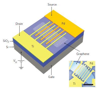
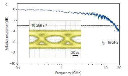

100 Photodiode based on graphene
101 Avalanche Photodiode Avalanche photodiodes (APDs) are preferred when the amount of optical power that can be spared for the receiver is limited. Their responsivity can significantly exceed 1 due to built in gain. The physical phenomenon behind the gain is known as impact ionization. Under certain conditions an accelerating electron can acquire sufficient energy to generate a new electron-hole pair. The net result is that a single primary electron creates many secondary electrons and holes, all of which contribute to the current. The generation rate is governed by two parameters, α e and α h, the impact-ionization coefficients for electrons and holes, respectively. Their numerical values depend on the semiconductor material and on the electric field that accelerates electrons and holes. Figure below shows the coefficients for several semiconductors. The values for α e and α h ~ 1x10⁻⁴ cm -1 are obtained for electric fields in the range of 2 4 x 10 5 V/m. Such high fields are obtained by applying a high voltage of ( ~ 100 V) to the APD. These values decreases with increasing temperature.
102 Avalanche Photodiodes Impact ionization processes resulting avalanche multiplication Electrode SiO 2 I photo R E h + e h > E g n+ p e h+ p+ E Electrode n + p Avalanche region e - E c x h + E v E(x) Impact of an energetic electron's kinetic energy excites VB electron to the CV. Absorption region Avalanche region x
103 Photodetector Noise Shot noise: Shot noise is related to the statistical fluctuation in both the photocurrent and the dark current. The magnitude of the shot noise is expressed as the root mean square (rms) noise current: q is charge of electron, 1.6*10-19 C Thermal or Johnson noise: The shunt resistance in a photodetector has a Johnson noise associated with it. This is due to the thermal generation of carriers. The magnitude of this generated current noise is: k B is Boltzmann Constant k B = 1.38 *10-23 J/K
104 Photodetector Noise Total Noise The total noise current generated in a photodetector is determined by: Noise Equivalent Power (NEP) Noise Equivalent Power is the amount of incident light power on a photodetector, which generates a photocurrent equal to the noise current. NEP is defined as:


105 APD example


106 Electrical wiring Reverse biased photodetector
107 Electrical wiring Amplified photodetector
108 Introduction to Network Modulation formats Signal multiplexing Time Code Wavelength System performance Bit Error Rate Optical signal to noise ratio Eye diagram Network architecture, limitation CIAN
109 System Performance Important parameters of a digital communication system Bit error rate: BER Optical signal to noise: OSNR Q factor All parameters are monitored regularly to track the health of the network Parameters are related to each other
110 Bit Error Rate Bit error rate (BER): One of the most important ways to determine the quality of a digital transmission system is to measure its Bit Error Rate (BER). BER is calculated by comparing the transmitted sequence of bits to the received bits and counting the number of errors. The ratio of how many bits received in error over the number of total bits received is the BER. This measured ratio is affected by many factors including: signal to noise ratio, distortion, and jitter. BER = N err /N bits For a good system performance BER < 10-12

111 Bit Error Testing-Eye diagram An eye diagram is a common indicator of the quality of signals in high-speed digital transmissions. An oscilloscope generates an eye diagram by overlaying sweeps of different segments of a long data stream driven by a master clock. In practical terms this may be achieved by displaying the data waveform on a sampling oscilloscope triggered from the system clock.
 at the input of the decision circuit in the receiver terminal Rx.")
112 Q-factor The performance of digital fiber-optic transmission systems can be specified using the Q-factor. The Q-factor is the electrical signal-to-noise ratio (SNR) at the input of the decision circuit in the receiver terminal Rx. For the purpose of calculation, the signal level is interpreted as the difference in the mean values 0 and 1, and the noise level is the sum of the standard deviations 0 and 1 at the sampling time: Q-factor
113 Bit Error Testing-Eye diagram BER is a conditional probability of receiving signal y while the transmitted signal is x, P(y/x), where x and y can each be digital 0 or 1. Since the transmitted signal digital states can be either 0 or 1, we can define P(y/0) and P(y/1) as the PDFs (probability density function) of the received signal at state y while the transmitted signals are 0 and 1, respectively. Suppose that the probability of sending digital 0 and 1 are P(O) and P(1) and the decision threshold is v th ; the BER of the receiver should be:,if Gaussian noise is assumed
114 Bit Error Testing-Eye diagram The probability for the receiver to declare 1 while the transmitter actually sends a 0 is: Where,,Q-value or quality factor Similarly, the probability for the receiver to declare 0 while the transmitter actually sends a 1 is:,p(0) = P (1) = 0.5 is assumed
115 Bit Error Testing-Eye diagram A widely used mathematical function, the error function, is defined as: And the complementary error function is defined as:
116 Bit Error Testing-Eye diagram By symmetry, we can assume Q 1 = Q 0 = Q, or,where BER as the function of the Q-value
OPTI510R: Photonics. Khanh Kieu College of Optical Sciences, University of Arizona Meinel building R.626
 OPTI510R: Photonics Khanh Kieu College of Optical Sciences, University of Arizona kkieu@optics.arizona.edu Meinel building R.626 Photodetectors Introduction Most important characteristics Photodetector
OPTI510R: Photonics. Khanh Kieu College of Optical Sciences, University of Arizona Meinel building R.626
 OPTI510R: Photonics Khanh Kieu College of Optical Sciences, University of Arizona kkieu@optics.arizona.edu Meinel building R.626 Announcements HW #5 is assigned (due April 9) April 9 th class will be in
Optical Amplifiers Photonics and Integrated Optics (ELEC-E3240) Zhipei Sun Photonics Group Department of Micro- and Nanosciences Aalto University
 Zhipei Sun Photonics Group Department of Micro- and Nanosciences Aalto University") Photonics Group Department of Micro- and Nanosciences Aalto University Optical Amplifiers Photonics and Integrated Optics (ELEC-E3240) Zhipei Sun Last Lecture Topics Course introduction Ray optics & optical
Photonics Group Department of Micro- and Nanosciences Aalto University Optical Amplifiers Photonics and Integrated Optics (ELEC-E3240) Zhipei Sun Last Lecture Topics Course introduction Ray optics & optical
Optodevice Data Book ODE I. Rev.9 Mar Opnext Japan, Inc.
 Optodevice Data Book ODE-408-001I Rev.9 Mar. 2003 Opnext Japan, Inc. Section 1 Operating Principles 1.1 Operating Principles of Laser Diodes (LDs) and Infrared Emitting Diodes (IREDs) 1.1.1 Emitting Principles
Optical Amplifiers. Continued. Photonic Network By Dr. M H Zaidi
 Optical Amplifiers Continued EDFA Multi Stage Designs 1st Active Stage Co-pumped 2nd Active Stage Counter-pumped Input Signal Er 3+ Doped Fiber Er 3+ Doped Fiber Output Signal Optical Isolator Optical
CONTENTS. Chapter 1 Wave Nature of Light 19
 CONTENTS Chapter 1 Wave Nature of Light 19 1.1 Light Waves in a Homogeneous Medium 19 A. Plane Electromagnetic Wave 19 B. Maxwell's Wave Equation and Diverging Waves 22 Example 1.1.1 A diverging laser
OPTI510R: Photonics. Khanh Kieu College of Optical Sciences, University of Arizona Meinel building R.626
 OPTI510R: Photonics Khanh Kieu College of Optical Sciences, University of Arizona kkieu@optics.arizona.edu Meinel building R.626 Announcements Homework #4 is due today, HW #5 is assigned (due April 8)
Chapter 12: Optical Amplifiers: Erbium Doped Fiber Amplifiers (EDFAs)
") Chapter 12: Optical Amplifiers: Erbium Doped Fiber Amplifiers (EDFAs) Prof. Dr. Yaocheng SHI ( 时尧成 ) yaocheng@zju.edu.cn http://mypage.zju.edu.cn/yaocheng 1 Traditional Optical Communication System Loss
Chapter 12: Optical Amplifiers: Erbium Doped Fiber Amplifiers (EDFAs) Prof. Dr. Yaocheng SHI ( 时尧成 ) yaocheng@zju.edu.cn http://mypage.zju.edu.cn/yaocheng 1 Traditional Optical Communication System Loss
Introduction Fundamentals of laser Types of lasers Semiconductor lasers
 ECE 5368 Introduction Fundamentals of laser Types of lasers Semiconductor lasers Introduction Fundamentals of laser Types of lasers Semiconductor lasers How many types of lasers? Many many depending on
Optical Fibers p. 1 Basic Concepts p. 1 Step-Index Fibers p. 2 Graded-Index Fibers p. 4 Design and Fabrication p. 6 Silica Fibers p.
 Preface p. xiii Optical Fibers p. 1 Basic Concepts p. 1 Step-Index Fibers p. 2 Graded-Index Fibers p. 4 Design and Fabrication p. 6 Silica Fibers p. 6 Plastic Optical Fibers p. 9 Microstructure Optical
Optical Receivers Theory and Operation
 Optical Receivers Theory and Operation Photo Detectors Optical receivers convert optical signal (light) to electrical signal (current/voltage) Hence referred O/E Converter Photodetector is the fundamental
OFCS OPTICAL DETECTORS 11/9/2014 LECTURES 1
 OFCS OPTICAL DETECTORS 11/9/2014 LECTURES 1 1-Defintion & Mechanisms of photodetection It is a device that converts the incident light into electrical current External photoelectric effect: Electrons are
Absorption: in an OF, the loss of Optical power, resulting from conversion of that power into heat.
 Absorption: in an OF, the loss of Optical power, resulting from conversion of that power into heat. Scattering: The changes in direction of light confined within an OF, occurring due to imperfection in
Elements of Optical Networking
 Bruckner Elements of Optical Networking Basics and practice of optical data communication With 217 Figures, 13 Tables and 93 Exercises Translated by Patricia Joliet VIEWEG+ TEUBNER VII Content Preface
Basic concepts. Optical Sources (b) Optical Sources (a) Requirements for light sources (b) Requirements for light sources (a)
 Optical Sources (a) Requirements for light sources (b) Requirements for light sources (a)") Optical Sources (a) Optical Sources (b) The main light sources used with fibre optic systems are: Light-emitting diodes (LEDs) Semiconductor lasers (diode lasers) Fibre laser and other compact solid-state
Optical Sources (a) Optical Sources (b) The main light sources used with fibre optic systems are: Light-emitting diodes (LEDs) Semiconductor lasers (diode lasers) Fibre laser and other compact solid-state
Lecture 6 Fiber Optical Communication Lecture 6, Slide 1
 Lecture 6 Optical transmitters Photon processes in light matter interaction Lasers Lasing conditions The rate equations CW operation Modulation response Noise Light emitting diodes (LED) Power Modulation
Lecture 18: Photodetectors
 Lecture 18: Photodetectors Contents 1 Introduction 1 2 Photodetector principle 2 3 Photoconductor 4 4 Photodiodes 6 4.1 Heterojunction photodiode.................... 8 4.2 Metal-semiconductor photodiode................
ECE 340 Lecture 29 : LEDs and Lasers Class Outline:
 ECE 340 Lecture 29 : LEDs and Lasers Class Outline: Light Emitting Diodes Lasers Semiconductor Lasers Things you should know when you leave Key Questions What is an LED and how does it work? How does a
Key Questions. What is an LED and how does it work? How does a laser work? How does a semiconductor laser work? ECE 340 Lecture 29 : LEDs and Lasers
 Things you should know when you leave Key Questions ECE 340 Lecture 29 : LEDs and Class Outline: What is an LED and how does it How does a laser How does a semiconductor laser How do light emitting diodes
EE 233. LIGHTWAVE. Chapter 2. Optical Fibers. Instructor: Ivan P. Kaminow
 EE 233. LIGHTWAVE SYSTEMS Chapter 2. Optical Fibers Instructor: Ivan P. Kaminow PLANAR WAVEGUIDE (RAY PICTURE) Agrawal (2004) Kogelnik PLANAR WAVEGUIDE a = (n s 2 - n c2 )/ (n f 2 - n s2 ) = asymmetry;
Figure Responsivity (A/W) Figure E E-09.
 Figure E E-09.") OSI Optoelectronics, is a leading manufacturer of fiber optic components for communication systems. The products offer range for Silicon, GaAs and InGaAs to full turnkey solutions. Photodiodes are semiconductor
OSI Optoelectronics, is a leading manufacturer of fiber optic components for communication systems. The products offer range for Silicon, GaAs and InGaAs to full turnkey solutions. Photodiodes are semiconductor
Review of Semiconductor Physics
 Review of Semiconductor Physics k B 1.38 u 10 23 JK -1 a) Energy level diagrams showing the excitation of an electron from the valence band to the conduction band. The resultant free electron can freely
Figure Figure E E-09. Dark Current (A) 1.
 1.") OSI Optoelectronics, is a leading manufacturer of fiber optic components for communication systems. The products offer range for Silicon, GaAs and InGaAs to full turnkey solutions. Photodiodes are semiconductor
OSI Optoelectronics, is a leading manufacturer of fiber optic components for communication systems. The products offer range for Silicon, GaAs and InGaAs to full turnkey solutions. Photodiodes are semiconductor
Performance Limitations of WDM Optical Transmission System Due to Cross-Phase Modulation in Presence of Chromatic Dispersion
 Performance Limitations of WDM Optical Transmission System Due to Cross-Phase Modulation in Presence of Chromatic Dispersion M. A. Khayer Azad and M. S. Islam Institute of Information and Communication
Fiberoptic Communication Systems By Dr. M H Zaidi. Optical Amplifiers
 Optical Amplifiers Optical Amplifiers Optical signal propagating in fiber suffers attenuation Optical power level of a signal must be periodically conditioned Optical amplifiers are a key component in
Introduction Fundamental of optical amplifiers Types of optical amplifiers
 ECE 6323 Introduction Fundamental of optical amplifiers Types of optical amplifiers Erbium-doped fiber amplifiers Semiconductor optical amplifier Others: stimulated Raman, optical parametric Advanced application:
Fiber-Optic Communication Systems
 Fiber-Optic Communication Systems Second Edition GOVIND P. AGRAWAL The Institute of Optics University of Rochester Rochester, NY A WILEY-iNTERSCIENCE PUBLICATION JOHN WILEY & SONS, INC. NEW YORK / CHICHESTER
Photodiode: LECTURE-5
 LECTURE-5 Photodiode: Photodiode consists of an intrinsic semiconductor sandwiched between two heavily doped p-type and n-type semiconductors as shown in Fig. 3.2.2. Sufficient reverse voltage is applied
Advanced Optical Communications Prof. R. K. Shevgaonkar Department of Electrical Engineering Indian Institute of Technology, Bombay
 Advanced Optical Communications Prof. R. K. Shevgaonkar Department of Electrical Engineering Indian Institute of Technology, Bombay Lecture No. # 27 EDFA In the last lecture, we talked about wavelength
Types of losses in optical fiber cable are: Due to attenuation, the power of light wave decreases exponentially with distance.
 UNIT-II TRANSMISSION CHARACTERISTICS OF OPTICAL FIBERS SIGNAL ATTENUATION: Signal attenuation in an optical fiber is defined as the decrease in light power during light propagation along an optical fiber.
Examination Optoelectronic Communication Technology. April 11, Name: Student ID number: OCT1 1: OCT 2: OCT 3: OCT 4: Total: Grade:
 Examination Optoelectronic Communication Technology April, 26 Name: Student ID number: OCT : OCT 2: OCT 3: OCT 4: Total: Grade: Declaration of Consent I hereby agree to have my exam results published on
Optical Communications and Networking 朱祖勍. Sept. 25, 2017
 Optical Communications and Networking Sept. 25, 2017 Lecture 4: Signal Propagation in Fiber 1 Nonlinear Effects The assumption of linearity may not always be valid. Nonlinear effects are all related to
Photonics (OPTI 510R 2017) - Final exam. (May 8, 10:30am-12:30pm, R307)
 - Final exam. (May 8, 10:30am-12:30pm, R307)") Photonics (OPTI 510R 2017) - Final exam (May 8, 10:30am-12:30pm, R307) Problem 1: (30pts) You are tasked with building a high speed fiber communication link between San Francisco and Tokyo (Japan) which
Photonics (OPTI 510R 2017) - Final exam (May 8, 10:30am-12:30pm, R307) Problem 1: (30pts) You are tasked with building a high speed fiber communication link between San Francisco and Tokyo (Japan) which
Guided Propagation Along the Optical Fiber
 Guided Propagation Along the Optical Fiber The Nature of Light Quantum Theory Light consists of small particles (photons) Wave Theory Light travels as a transverse electromagnetic wave Ray Theory Light
Optical Communications and Networking 朱祖勍. Oct. 9, 2017
 Optical Communications and Networking Oct. 9, 2017 1 Optical Amplifiers In optical communication systems, the optical signal from the transmitter are attenuated by the fiber and other passive components
UNIT-II : SIGNAL DEGRADATION IN OPTICAL FIBERS
 UNIT-II : SIGNAL DEGRADATION IN OPTICAL FIBERS The Signal Transmitting through the fiber is degraded by two mechanisms. i) Attenuation ii) Dispersion Both are important to determine the transmission characteristics
Guided Propagation Along the Optical Fiber. Xavier Fernando Ryerson Comm. Lab
 Guided Propagation Along the Optical Fiber Xavier Fernando Ryerson Comm. Lab The Nature of Light Quantum Theory Light consists of small particles (photons) Wave Theory Light travels as a transverse electromagnetic
UNIT-III SOURCES AND DETECTORS. According to the shape of the band gap as a function of the momentum, semiconductors are classified as
 UNIT-III SOURCES AND DETECTORS DIRECT AND INDIRECT BAND GAP SEMICONDUCTORS: According to the shape of the band gap as a function of the momentum, semiconductors are classified as 1. Direct band gap semiconductors
Semiconductor Lasers Semiconductors were originally pumped by lasers or e-beams First diode types developed in 1962: Create a pn junction in
 Semiconductor Lasers Semiconductors were originally pumped by lasers or e-beams First diode types developed in 1962: Create a pn junction in semiconductor material Pumped now with high current density
Photons and solid state detection
 Photons and solid state detection Photons represent discrete packets ( quanta ) of optical energy Energy is hc/! (h: Planck s constant, c: speed of light,! : wavelength) For solid state detection, photons
Photonics and Optical Communication Spring 2005
 Photonics and Optical Communication Spring 2005 Final Exam Instructor: Dr. Dietmar Knipp, Assistant Professor of Electrical Engineering Name: Mat. -Nr.: Guidelines: Duration of the Final Exam: 2 hour You
S Optical Networks Course Lecture 2: Essential Building Blocks
 S-72.3340 Optical Networks Course Lecture 2: Essential Building Blocks Edward Mutafungwa Communications Laboratory, Helsinki University of Technology, P. O. Box 2300, FIN-02015 TKK, Finland Tel: +358 9
Chapter 3 OPTICAL SOURCES AND DETECTORS
 Chapter 3 OPTICAL SOURCES AND DETECTORS 3. Optical sources and Detectors 3.1 Introduction: The success of light wave communications and optical fiber sensors is due to the result of two technological breakthroughs.
Dr. Monir Hossen ECE, KUET
 Dr. Monir Hossen ECE, KUET 1 Outlines of the Class Principles of WDM DWDM, CWDM, Bidirectional WDM Components of WDM AWG, filter Problems with WDM Four-wave mixing Stimulated Brillouin scattering WDM Network
FIBER OPTICS. Prof. R.K. Shevgaonkar. Department of Electrical Engineering. Indian Institute of Technology, Bombay. Lecture: 20
 FIBER OPTICS Prof. R.K. Shevgaonkar Department of Electrical Engineering Indian Institute of Technology, Bombay Lecture: 20 Photo-Detectors and Detector Noise Fiber Optics, Prof. R.K. Shevgaonkar, Dept.
Detectors for Optical Communications
 Optical Communications: Circuits, Systems and Devices Chapter 3: Optical Devices for Optical Communications lecturer: Dr. Ali Fotowat Ahmady Sep 2012 Sharif University of Technology 1 Photo All detectors
Practical Aspects of Raman Amplifier
 Practical Aspects of Raman Amplifier Contents Introduction Background Information Common Types of Raman Amplifiers Principle Theory of Raman Gain Noise Sources Related Information Introduction This document
Chapter 8. Wavelength-Division Multiplexing (WDM) Part II: Amplifiers
 Part II: Amplifiers") Chapter 8 Wavelength-Division Multiplexing (WDM) Part II: Amplifiers Introduction Traditionally, when setting up an optical link, one formulates a power budget and adds repeaters when the path loss exceeds
Chapter 8 Wavelength-Division Multiplexing (WDM) Part II: Amplifiers Introduction Traditionally, when setting up an optical link, one formulates a power budget and adds repeaters when the path loss exceeds
Optical Fibre Amplifiers Continued
 1 Optical Fibre Amplifiers Continued Stavros Iezekiel Department of Electrical and Computer Engineering University of Cyprus ECE 445 Lecture 09 Fall Semester 2016 2 ERBIUM-DOPED FIBRE AMPLIFIERS BASIC
Semiconductor Lasers Semiconductors were originally pumped by lasers or e-beams First diode types developed in 1962: Create a pn junction in
 Semiconductor Lasers Semiconductors were originally pumped by lasers or e-beams First diode types developed in 1962: Create a pn junction in semiconductor material Pumped now with high current density
OPTOELECTRONIC and PHOTOVOLTAIC DEVICES
 OPTOELECTRONIC and PHOTOVOLTAIC DEVICES Outline 1. Introduction to the (semiconductor) physics: energy bands, charge carriers, semiconductors, p-n junction, materials, etc. 2. Light emitting diodes Light
The absorption of the light may be intrinsic or extrinsic
 Attenuation Fiber Attenuation Types 1- Material Absorption losses 2- Intrinsic Absorption 3- Extrinsic Absorption 4- Scattering losses (Linear and nonlinear) 5- Bending Losses (Micro & Macro) Material
Performance Analysis of Designing a Hybrid Optical Amplifier (HOA) for 32 DWDM Channels in L-band by using EDFA and Raman Amplifier
 for 32 DWDM Channels in L-band by using EDFA and Raman Amplifier") Performance Analysis of Designing a Hybrid Optical Amplifier (HOA) for 32 DWDM Channels in L-band by using EDFA and Raman Amplifier Aied K. Mohammed, PhD Department of Electrical Engineering, University
Performance Analysis of Designing a Hybrid Optical Amplifier (HOA) for 32 DWDM Channels in L-band by using EDFA and Raman Amplifier Aied K. Mohammed, PhD Department of Electrical Engineering, University
Lecture 3 Fiber Optical Communication Lecture 3, Slide 1
 Lecture 3 Dispersion in single-mode fibers Material dispersion Waveguide dispersion Limitations from dispersion Propagation equations Gaussian pulse broadening Bit-rate limitations Fiber losses Fiber Optical
Guided Propagation Along the Optical Fiber. Xavier Fernando Ryerson University
 Guided Propagation Along the Optical Fiber Xavier Fernando Ryerson University The Nature of Light Quantum Theory Light consists of small particles (photons) Wave Theory Light travels as a transverse electromagnetic
Physics of Waveguide Photodetectors with Integrated Amplification
 Physics of Waveguide Photodetectors with Integrated Amplification J. Piprek, D. Lasaosa, D. Pasquariello, and J. E. Bowers Electrical and Computer Engineering Department University of California, Santa
Optical Transport Tutorial
 Optical Transport Tutorial 4 February 2015 2015 OpticalCloudInfra Proprietary 1 Content Optical Transport Basics Assessment of Optical Communication Quality Bit Error Rate and Q Factor Wavelength Division
Photonics and Optical Communication
 Photonics and Optical Communication (Course Number 300352) Spring 2007 Dr. Dietmar Knipp Assistant Professor of Electrical Engineering http://www.faculty.iu-bremen.de/dknipp/ 1 Photonics and Optical Communication
Optical Fiber Communication Lecture 11 Detectors
 Optical Fiber Communication Lecture 11 Detectors Warriors of the Net Detector Technologies MSM (Metal Semiconductor Metal) PIN Layer Structure Semiinsulating GaAs Contact InGaAsP p 5x10 18 Absorption InGaAs
CHAPTER 4 RESULTS. 4.1 Introduction
 CHAPTER 4 RESULTS 4.1 Introduction In this chapter focus are given more on WDM system. The results which are obtained mainly from the simulation work are presented. In simulation analysis, the study will
Notes on Optical Amplifiers
 Notes on Optical Amplifiers Optical amplifiers typically use energy transitions such as those in atomic media or electron/hole recombination in semiconductors. In optical amplifiers that use semiconductor
Fundamentals of CMOS Image Sensors
 CHAPTER 2 Fundamentals of CMOS Image Sensors Mixed-Signal IC Design for Image Sensor 2-1 Outline Photoelectric Effect Photodetectors CMOS Image Sensor(CIS) Array Architecture CIS Peripherals Design Considerations
EC Optical Communication And Networking TWO MARKS QUESTION AND ANSWERS UNIT -1 INTRODUCTION
 EC6702 - Optical Communication And Networking TWO MARKS QUESTION AND ANSWERS UNIT -1 INTRODUCTION Ray Theory Transmission 1. Write short notes on ray optics theory. Laws governing the nature of light are
is a method of transmitting information from one place to another by sending light through an optical fiber. The light forms an electromagnetic
 is a method of transmitting information from one place to another by sending light through an optical fiber. The light forms an electromagnetic carrier wave that is modulated to carry information. The
Lecture 8 Fiber Optical Communication Lecture 8, Slide 1
 Lecture 8 Bit error rate The Q value Receiver sensitivity Sensitivity degradation Extinction ratio RIN Timing jitter Chirp Forward error correction Fiber Optical Communication Lecture 8, Slide Bit error
Luminous Equivalent of Radiation
 Intensity vs λ Luminous Equivalent of Radiation When the spectral power (p(λ) for GaP-ZnO diode has a peak at 0.69µm) is combined with the eye-sensitivity curve a peak response at 0.65µm is obtained with
Analysis of Self Phase Modulation Fiber nonlinearity in Optical Transmission System with Dispersion
 36 Analysis of Self Phase Modulation Fiber nonlinearity in Optical Transmission System with Dispersion Supreet Singh 1, Kulwinder Singh 2 1 Department of Electronics and Communication Engineering, Punjabi
Photonics and Fiber Optics
 1 UNIT V Photonics and Fiber Optics Part-A 1. What is laser? LASER is the acronym for Light Amplification by Stimulated Emission of Radiation. The absorption and emission of light by materials has been
Fiber-based components. by: Khanh Kieu
 Fiber-based components by: Khanh Kieu Projects 1. Handling optical fibers, numerical aperture 2. Measurement of fiber attenuation 3. Connectors and splices 4. Free space coupling of laser into fibers 5.
DESIGN TEMPLATE ISSUES ANALYSIS FOR ROBUST DESIGN OUTPUT. performance, yield, reliability
 DESIGN TEMPLATE ISSUES performance, yield, reliability ANALYSIS FOR ROBUST DESIGN properties, figure-of-merit thermodynamics, kinetics, process margins process control OUTPUT models, options Optical Amplification
NON-AMPLIFIED PHOTODETECTOR USER S GUIDE
 NON-AMPLIFIED PHOTODETECTOR USER S GUIDE Thank you for purchasing your Non-amplified Photodetector. This user s guide will help answer any questions you may have regarding the safe use and optimal operation
Light Sources, Modulation, Transmitters and Receivers
 Optical Fibres and Telecommunications Light Sources, Modulation, Transmitters and Receivers Introduction Previous section looked at Fibres. How is light generated in the first place? How is light modulated?
Optical Communications
 Optical Communications Telecommunication Engineering School of Engineering University of Rome La Sapienza Rome, Italy 2005-2006 Lecture #4, May 9 2006 Receivers OVERVIEW Photodetector types: Photodiodes
InP-based Waveguide Photodetector with Integrated Photon Multiplication
 InP-based Waveguide Photodetector with Integrated Photon Multiplication D.Pasquariello,J.Piprek,D.Lasaosa,andJ.E.Bowers Electrical and Computer Engineering Department University of California, Santa Barbara,
21. (i) Briefly explain the evolution of fiber optic system (ii) Compare the configuration of different types of fibers. or 22. (b)(i) Derive modal eq
 Briefly explain the evolution of fiber optic system (ii) Compare the configuration of different types of fibers. or 22. (b)(i) Derive modal eq") Unit-1 Part-A FATIMA MICHAEL COLLEGE OF ENGINEERING & TECHNOLOGY Senkottai Village, Madurai Sivagangai Main Road, Madurai - 625 020. [An ISO 9001:2008 Certified Institution] DEPARTMENT OF ELECTRONICS AND
Unit-1 Part-A FATIMA MICHAEL COLLEGE OF ENGINEERING & TECHNOLOGY Senkottai Village, Madurai Sivagangai Main Road, Madurai - 625 020. [An ISO 9001:2008 Certified Institution] DEPARTMENT OF ELECTRONICS AND
Homework Set 3.5 Sensitive optoelectronic detectors: seeing single photons
 Homework Set 3.5 Sensitive optoelectronic detectors: seeing single photons Due by 12:00 noon (in class) on Tuesday, Nov. 7, 2006. This is another hybrid lab/homework; please see Section 3.4 for what you
Lecture 9 External Modulators and Detectors
 Optical Fibres and Telecommunications Lecture 9 External Modulators and Detectors Introduction Where are we? A look at some real laser diodes. External modulators Mach-Zender Electro-absorption modulators
14.2 Photodiodes 411
 14.2 Photodiodes 411 Maximum reverse voltage is specified for Ge and Si photodiodes and photoconductive cells. Exceeding this voltage can cause the breakdown and severe deterioration of the sensor s performance.
Engineering Medical Optics BME136/251 Winter 2018
 Engineering Medical Optics BME136/251 Winter 2018 Monday/Wednesday 2:00-3:20 p.m. Beckman Laser Institute Library, MSTB 214 (lab) *1/17 UPDATE Wednesday, 1/17 Optics and Photonic Devices III: homework
Optical Communication and Networks M.N. Bandyopadhyay
 Optical Communication and Networks M.N. Bandyopadhyay Director National Institute of Technology (NIT) Calicut Delhi-110092 2014 OPTICAL COMMUNICATION AND NETWORKS M.N. Bandyopadhyay 2014 by PHI Learning
Fiber Amplifiers. Fiber Lasers. 1*5 World Scientific. Niloy K nulla. University ofconnecticut, USA HONG KONG NEW JERSEY LONDON
 LONDON Fiber Amplifiers Fiber Lasers Niloy K nulla University ofconnecticut, USA 1*5 World Scientific NEW JERSEY SINGAPORE BEIJING SHANGHAI HONG KONG TAIPEI CHENNAI Contents Preface v 1. Introduction 1
OPTI510R: Photonics. Khanh Kieu College of Optical Sciences, University of Arizona Meinel building R.626
 OPTI510R: Photonics Khanh Kieu College of Optical Sciences, University of Arizona kkieu@optics.arizona.edu Meinel building R.626 Announcements Homework #3 is due today No class Monday, Feb 26 Pre-record
Optical Amplifiers (Chapter 6)
") Optical Amplifiers (Chapter 6) General optical amplifier theory Semiconductor Optical Amplifier (SOA) Raman Amplifiers Erbium-doped Fiber Amplifiers (EDFA) Read Chapter 6, pp. 226-266 Loss & dispersion
Optical Amplifiers (Chapter 6) General optical amplifier theory Semiconductor Optical Amplifier (SOA) Raman Amplifiers Erbium-doped Fiber Amplifiers (EDFA) Read Chapter 6, pp. 226-266 Loss & dispersion
Optical switches. Switching Technology S Optical switches
 Optical switches Switching Technology S38.165 http://www.netlab.hut.fi/opetus/s38165 13-1 Optical switches Components and enabling technologies Contention resolution Optical switching schemes 13-2 1 Components
Safa O. Kasap Electrical Engineering Department, University of Saskatchewan, Saskatoon, S7N 5A9, Canada
 1 Optoelectronics Safa O. Kasap Electrical Engineering Department, University of Saskatchewan, Saskatoon, S7N 5A9, Canada e-mail: kasap@engr.usask.ca Abstract It is useful to view today s optoelectronics
Optical Fiber Technology. Photonic Network By Dr. M H Zaidi
 Optical Fiber Technology Numerical Aperture (NA) What is numerical aperture (NA)? Numerical aperture is the measure of the light gathering ability of optical fiber The higher the NA, the larger the core
FIBER OPTICS. Prof. R.K. Shevgaonkar. Department of Electrical Engineering. Indian Institute of Technology, Bombay. Lecture: 37
 FIBER OPTICS Prof. R.K. Shevgaonkar Department of Electrical Engineering Indian Institute of Technology, Bombay Lecture: 37 Introduction to Raman Amplifiers Fiber Optics, Prof. R.K. Shevgaonkar, Dept.
Suppression of Stimulated Brillouin Scattering
 Suppression of Stimulated Brillouin Scattering 42 2 5 W i de l y T u n a b l e L a s e r T ra n s m i t te r www.lumentum.com Technical Note Introduction This technical note discusses the phenomenon and
Dr. Rüdiger Paschotta RP Photonics Consulting GmbH. Competence Area: Fiber Devices
 Dr. Rüdiger Paschotta RP Photonics Consulting GmbH Competence Area: Fiber Devices Topics in this Area Fiber lasers, including exotic types Fiber amplifiers, including telecom-type devices and high power
Recent Development and Study of Silicon Solid State Photomultiplier (MRS Avalanche Photodetector)
") Recent Development and Study of Silicon Solid State Photomultiplier (MRS Avalanche Photodetector) Valeri Saveliev University of Obninsk, Russia Vienna Conference on Instrumentation Vienna, 20 February
Recent Development and Study of Silicon Solid State Photomultiplier (MRS Avalanche Photodetector) Valeri Saveliev University of Obninsk, Russia Vienna Conference on Instrumentation Vienna, 20 February
Functional Materials. Optoelectronic devices
 Functional Materials Lecture 2: Optoelectronic materials and devices (inorganic). Photonic materials Optoelectronic devices Light-emitting diode (LED) displays Photodiode and Solar cell Photoconductive
Investigate the characteristics of PIN Photodiodes and understand the usage of the Lightwave Analyzer component.
 PIN Photodiode 1 OBJECTIVE Investigate the characteristics of PIN Photodiodes and understand the usage of the Lightwave Analyzer component. 2 PRE-LAB In a similar way photons can be generated in a semiconductor,
2 in the multipath dispersion of the optical fibre. (b) Discuss the merits and drawbacks of cut bouls method of measurement of alternation.
 Discuss the merits and drawbacks of cut bouls method of measurement of alternation.") B.TECH IV Year I Semester (R09) Regular Examinations, November 2012 1 (a) Derive an expression for multiple time difference tt 2 in the multipath dispersion of the optical fibre. (b) Discuss the merits
B.TECH IV Year I Semester (R09) Regular Examinations, November 2012 1 (a) Derive an expression for multiple time difference tt 2 in the multipath dispersion of the optical fibre. (b) Discuss the merits
A continuous-wave Raman silicon laser
 A continuous-wave Raman silicon laser Haisheng Rong, Richard Jones,.. - Intel Corporation Ultrafast Terahertz nanoelectronics Lab Jae-seok Kim 1 Contents 1. Abstract 2. Background I. Raman scattering II.
CONTENTS. 2.2 Schrodinger's Wave Equation 31. PART I Semiconductor Material Properties. 2.3 Applications of Schrodinger's Wave Equation 34
 CONTENTS Preface x Prologue Semiconductors and the Integrated Circuit xvii PART I Semiconductor Material Properties CHAPTER 1 The Crystal Structure of Solids 1 1.0 Preview 1 1.1 Semiconductor Materials
Optical communications
 Optical communications Components and enabling technologies Optical networking Evolution of optical networking: road map SDH = Synchronous Digital Hierarchy SONET = Synchronous Optical Network SDH SONET
Components of Optical Instruments. Chapter 7_III UV, Visible and IR Instruments
 Components of Optical Instruments Chapter 7_III UV, Visible and IR Instruments 1 Grating Monochromators Principle of operation: Diffraction Diffraction sources: grooves on a reflecting surface Fabrication:
LEDs, Photodetectors and Solar Cells
 LEDs, Photodetectors and Solar Cells Chapter 7 (Parker) ELEC 424 John Peeples Why the Interest in Photons? Answer: Momentum and Radiation High electrical current density destroys minute polysilicon and
UNIT VIII-SPECIAL PURPOSE ELECTRONIC DEVICES. 1. Explain tunnel Diode operation with the help of energy band diagrams.
 UNIT III-SPECIAL PURPOSE ELECTRONIC DEICES 1. Explain tunnel Diode operation with the help of energy band diagrams. TUNNEL DIODE: A tunnel diode or Esaki diode is a type of semiconductor diode which is
Chap14. Photodiode Detectors
 Chap14. Photodiode Detectors Mohammad Ali Mansouri-Birjandi mansouri@ece.usb.ac.ir mamansouri@yahoo.com Faculty of Electrical and Computer Engineering University of Sistan and Baluchestan (USB) Design