LOW-DROPOUT VOLTAGE REGULATORS
|
|
|
- Daniela Melina Waters
- 6 years ago
- Views:
Transcription
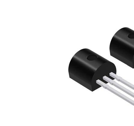
1 1 TL750L TL751L SLVS017U SEPTEMBER 1987 REVISED SEPTEMBER 2009 LOW-DROPOUT VOLTAGE REGULATORS 1FEATURES Very Low Dropout Voltage, Less Than 0.6 V at Reverse Transient Protection Down to 50 V 150 ma Internal Thermal-Overload Protection Very Low Quiescent Current Overvoltage Protection TTL- and CMOS-Compatible Enable on TL751L Internal Overcurrent-Limiting Circuitry Series Less Than 500-μA Disable (TL751L Series) 60-V Load-Dump Protection OUTPUT NC TL750L... D PACKAGE (TOP VIEW) INPUT NC TL750L... KC PACKAGE (TOP VIEW) OUTPUT INPUT TL750L... KCS PACKAGE (TOP VIEW) OUTPUT INPUT NC No internal connection TL750L... KTE PACKAGE (TOP VIEW) TL750L... KTT PACKAGE (TOP VIEW) TL750L... KVU PACKAGE (TOP VIEW) OUTPUT INPUT OUTPUT INPUT OUTPUT INPUT TL750L... LP PACKAGE (TO-92, TO-226AA) (TOP VIEW) INPUT OUTPUT OUTPUT NC TL751L... D PACKAGE (TOP VIEW) INPUT ENABLE NC No internal connection OUTPUT NC NC NC TL751L...P PACKAGE (TOP VIEW) NC No internal connection INPUT NC ENABLE DESCRIPTION/ORDERING INFORMATION The TL750L and TL751L series of fixed-output voltage regulators offer 5-V, 8-V, 10-V, and 12-V options. The TL751L series also has an enable (ENABLE) input. When ENABLE is high, the regulator output is placed in the high-impedance state. This gives the designer complete control over power up, power down, or emergency shutdown. The TL750L and TL751L series are low-dropout positive-voltage regulators specifically designed for battery-powered systems. These devices incorporate overvoltage and current-limiting protection circuitry, along with internal reverse-battery protection circuitry to protect the devices and the regulated system. The series is fully protected against 60-V load-dump and reverse-battery conditions. Extremely low quiescent current during full-load conditions makes these devices ideal for standby power systems. Please be aware that an important notice concerning availability, standard warranty, and use in critical applications of Texas Instruments semiconductor products and disclaimers thereto appears at the end of this data sheet. PRODUCTION DATA information is current as of publication date. Products conform to specifications per the terms of the Texas Instruments standard warranty. Production processing does not necessarily include testing of all parameters. Copyright , Texas Instruments Incorporated
2 TL750L TL751L SLVS017U SEPTEMBER 1987 REVISED SEPTEMBER ORDERING INFORMATION (1) V O TYP T J PACKAGE (2) ORDERABLE PART NUMBER TOP-SIDE MARKING AT 25 C 0 C to 125 C PowerFLEX KTE Reel of 2000 TL750L05CKTER TL750L05C SOIC D Tube of 75 Reel of 2500 Tube of 75 Reel of 2500 TL750L05CD TL750L05CDR TL751L05CD TL751L05CDR 5 V Bulk of 1000 TL750L05CLP TO-226/TO-92 LP Reel of 2000 TL750L05CLPR 50L05C 51L05C 750L05C TO-220 KC Tube of 50 TL750L05CKC TL750L05C TO-220 KCS Tube of 50 TL750L05CKCS TL750L05C TO-252 KVU Reel of 2500 TL750L05CKVUR 750L05C TO-263 KTT Reel of 500 TL750L05CKTTR 750L05C Tube of 75 TL750L08CD SOIC D 8 V Reel of 2500 TL750L08CDR 50L08C TO-226/TO-92 LP Bulk of 1000 TL750L08CLP 750L08C PDIP P Tube of 50 TL751L10CP TL751L10C Tube of 75 TL750L10CD Reel of 2500 TL750L10CDR SOIC D 10 V Tube of 75 TL751L10CD TO-226/TO-92 LP Reel of 2500 Bulk of 1000 Reel of 2000 Tube of 75 TL751L10CDR TL750L10CLP TL750L10CLPR TL750L12CD Reel of 2500 TL750L12CDR SOIC D 12 V Tube of 75 TL751L12CD Reel of 2500 TL751L12CDR 50L10C 51L10C 750L10C 50L12C 51L12C TO-226/TO-92 LP Bulk of 1000 TL750L12CLP 750L12C (1) For the most current package and ordering information, see the Package Option Addendum at the end of this document, or see the TI web site at (2) Package drawings, thermal data, and symbolization are available at DEVICE COMPONENT COUNT Transistors 20 JFETs 2 Diodes 5 Resistors 16 2 Submit Documentation Feedback Copyright , Texas Instruments Incorporated
3 TL750L TL751L SLVS017U SEPTEMBER 1987 REVISED SEPTEMBER 2009 Absolute Maximum Ratings (1) over operating junction temperature range (unless otherwise noted) MIN MAX UNIT Continuous input voltage 26 V Transient input voltage (2) T A = 25 C 60 V Continuous reverse input voltage 15 V Transient reverse input voltage t 100 ms 50 V T J Operating virtual junction temperature 150 C Lead temperature 1,6 mm (1/16 in) for 10 s 260 C T stg Storage temperature range C (1) Stresses beyond those listed under "absolute maximum ratings" may cause permanent damage to the device. These are stress ratings only, and functional operation of the device at these or any other conditions beyond those indicated under "recommended operating conditions" is not implied. Exposure to absolute-maximum-rated conditions for extended periods may affect device reliability. (2) The transient input voltage rating applies to the waveform shown in Figure 1. Package Thermal Data (1) PACKAGE BOARD θ JC θ JA PDIP (P) High K, JESD C/W 85 C/W PowerFLEX (KTE) High K, JESD C/W 23 C/W SOIC (D) High K, JESD C/W 97 C/W TO-226/TO-92 (LP) High K, JESD C/W 140 C/W TO-220 (KC) High K, JESD C/W 19 C/W TO-220 (KCS) High K, JESD C/W 19 C/W TO-252 (KVU) High K, JESD C/W TO-263 (KTT) High K, JESD C/W 25.3 C/W (1) Maximum power dissipation is a function of T J (max), θ JA, and T A. The maximum allowable power dissipation at any allowable ambient temperature is P D = (T J (max) T A )/θ JA. Operating at the absolute maximum T J of 150 C can affect reliability. Recommended Operating Conditions over recommended operating junction temperature range (unless otherwise noted) MIN MAX UNIT TL75xL TL75xL V I Input voltage V TL75xL TL75xL V IH High-level ENABLE input voltage TL75xLxx 2 15 V V IL (1) Low-level ENABLE input voltage T J = 25 C TL75xLxx T J = 0 C to 125 C TL75xLxx I O Output current TL75xLxx ma T J Operating virtual junction temperature TL75xLxxC C (1) The algebraic convention, in which the least positive (most negative) value is designated minimum, is used in this data sheet for ENABLE voltage levels and temperature only. V Copyright , Texas Instruments Incorporated Submit Documentation Feedback 3
4 TL750L TL751L SLVS017U SEPTEMBER 1987 REVISED SEPTEMBER TL75xL05 Electrical Characteristics (1) V I = 14 V, I O = 10 ma, T J = 25 C (unless otherwise noted) PARAMETER TEST CONDITIONS TL750L05 TL751L05 UNIT MIN TYP MAX T J = 25 C Output voltage V I = 6 V to 26 V, I O = 0 to 150 ma V T J = 0 C to 125 C Input regulation voltage V I = 9 V to 16 V 5 10 V I = 6 V to 26 V 6 30 Ripple rejection V I = 8 V to 18 V, f = 120 Hz db Output regulation voltage I O = 5 ma to 150 ma mv Dropout voltage I O = 10 ma 0.2 I O = 150 ma 0.6 Output noise voltage f = 10 Hz to 100 khz 500 μv I O = 150 ma Quiescent current V I = 6 V to 26 V, I O = 10 ma, T J = 0 C to 125 C 1 2 ma ENABLE 2 V 0.5 (1) Pulse-testing techniques are used to maintain the junction temperature as close to the ambient temperature as possible. Thermal effects must be taken into account separately. All characteristics are measured with a 0.1-μF capacitor across the input and a 10-μF capacitor, with equivalent series resistance of less than 0.4 Ω, across the output. TL75xL08 Electrical Characteristics (1) V I = 14 V, I O = 10 ma, T J = 25 C (unless otherwise noted) PARAMETER TEST CONDITIONS TL750L08 TL751L08 UNIT MIN TYP MAX T J = 25 C Output voltage V I = 9 V to 26 V, I O = 0 to 150 ma V T J = 0 C to 125 C Input regulation voltage V I = 10 V to 17 V V I = 9 V to 26 V Ripple rejection V I = 11 V to 21 V, f = 120 Hz db Output regulation voltage I O = 5 ma to 150 ma mv Dropout voltage I O = 10 ma 0.2 I O = 150 ma 0.6 Output noise voltage f = 10 Hz to 100 khz 500 μv I O = 150 ma Quiescent current V I = 9 V to 26 V, I O = 10 ma, T J = 0 C to 125 C 1 2 ma ENABLE 2 V 0.5 (1) Pulse-testing techniques are used to maintain the junction temperature as close to the ambient temperature as possible. Thermal effects must be taken into account separately. All characteristics are measured with a 0.1-μF capacitor across the input and a 10-μF capacitor, with equivalent series resistance of less than 0.4 Ω, across the output. mv V mv V 4 Submit Documentation Feedback Copyright , Texas Instruments Incorporated
5 TL750L TL751L SLVS017U SEPTEMBER 1987 REVISED SEPTEMBER 2009 TL75xL10 Electrical Characteristics (1) V I = 14 V, I O = 10 ma, T J = 25 C (unless otherwise noted) PARAMETER TEST CONDITIONS TL750L10 TL751L10 UNIT MIN TYP MAX T J = 25 C Output voltage V I = 11 V to 26 V, I O = 0 to 150 ma V T J = 0 C to 125 C Input regulation voltage V I = 12 V to 19 V V I = 11 V to 26 V Ripple rejection V I = 12 V to 22 V, f = 120 Hz db Output regulation voltage I O = 5 ma to 150 ma mv Dropout voltage I O = 10 ma 0.2 I O = 150 ma 0.6 Output noise voltage f = 10 Hz to 100 khz 700 μv I O = 150 ma Quiescent current V I = 11 V to 26 V, I O = 10 ma, T J = 0 C to 125 C 1 2 ma ENABLE 2 V 0.5 (1) Pulse-testing techniques are used to maintain the junction temperature as close to the ambient temperature as possible. Thermal effects must be taken into account separately. All characteristics are measured with a 0.1-μF capacitor across the input and a 10-μF capacitor, with equivalent series resistance of less than 0.4 Ω, across the output. TL75xL12 Electrical Characteristics (1) V I = 14 V, I O = 10 ma, T J = 25 C (unless otherwise noted) PARAMETER TEST CONDITIONS TL750L12 TL751L12 UNIT MIN TYP MAX T J = 25 C Output voltage V I = 13 V to 26 V, I O = 0 to 150 ma V T J = 0 C to 125 C Input regulation voltage V I = 14 V to 19 V V I = 13 V to 26 V Ripple rejection V I = 13 V to 23 V, f = 120 Hz db Output regulation voltage I O = 5 ma to 150 ma mv Dropout voltage I O = 10 ma 0.2 I O = 150 ma 0.6 Output noise voltage f = 10 Hz to 100 khz 700 μv I O = 150 ma Quiescent current V I = 13 V to 26 V, I O = 10 ma, T J = 0 C to 125 C 1 2 ma ENABLE 2 V 0.5 (1) Pulse-testing techniques are used to maintain the junction temperature as close to the ambient temperature as possible. Thermal effects must be taken into account separately. All characteristics are measured with a 0.1-μF capacitor across the input and a 10-μF capacitor, with equivalent series resistance of less than 0.4 Ω, across the output. PARAMETER MEASUREMENT INFORMATION The TL750L, TL751L series are low-dropout regulators. This means that capacitance loading is important to the performance of the regulator because it is a vital part of the control loop. The capacitor value and its equivalent series resistance (ESR) both affect the control loop and must be defined for the load range and temperature range. Figure 1 shows the recommended range of ESR for a given load with a 10-μF capacitor on the output. mv V mv V Copyright , Texas Instruments Incorporated Submit Documentation Feedback 5
6 TL750L TL751L SLVS017U SEPTEMBER 1987 REVISED SEPTEMBER Ω ESR Equivalent Series Resistance TL750L05 EQUIVALENT SERIES RESISTANCE vs LOAD CURRENT C L = 10-µF Tantalum Capacitor T A = 40 C to 125 C Potential Instability Region Region of Best Stability Potential Instability Region I L Load Current ma TYPICAL CHARACTERISTICS V i Transient Input Voltage V TRANSIENT INPUT VOLTAGE vs TIME ÎÎÎ t r = 1 ms T A = 25 C V I = 14 V + 46e ( t/0.230) for t 5 ms t Time ms Figure 1. Figure TL750L05 INPUT CURRENT vs INPUT VOLTAGE 60 TL750L12 INPUT CURRENT vs INPUT VOLTAGE Input Current ma I I Input Current ma I I V I Input Voltage V Figure 3. Figure V I Input Voltage V 6 Submit Documentation Feedback Copyright , Texas Instruments Incorporated
7 PACKAGE OPTION ADDENDUM 17-Jul-2017 PACKAGING INFORMATION Orderable Device Status (1) Package Type Package Drawing Pins Package Qty Eco Plan TL750L05CD ACTIVE SOIC D 8 75 Green (RoHS TL750L05CDG4 ACTIVE SOIC D 8 75 Green (RoHS TL750L05CDR ACTIVE SOIC D Green (RoHS TL750L05CDRE4 ACTIVE SOIC D Green (RoHS TL750L05CKCS ACTIVE TO-220 KCS 3 50 Pb-Free (RoHS) TL750L05CKCSE3 ACTIVE TO-220 KCS 3 50 Pb-Free (RoHS) TL750L05CKTTR ACTIVE DDPAK/ TO-263 TL750L05CKTTRG3 ACTIVE DDPAK/ TO-263 (2) KTT Green (RoHS KTT Green (RoHS TL750L05CKVURG3 ACTIVE TO-252 KVU Green (RoHS TL750L05CLP ACTIVE TO-92 LP Pb-Free (RoHS) TL750L05CLPE3 ACTIVE TO-92 LP Pb-Free (RoHS) TL750L05CLPR ACTIVE TO-92 LP Pb-Free (RoHS) TL750L05CLPRE3 ACTIVE TO-92 LP Pb-Free (RoHS) TL750L08CD ACTIVE SOIC D 8 75 Green (RoHS TL750L08CDE4 ACTIVE SOIC D 8 75 Green (RoHS TL750L08CDG4 ACTIVE SOIC D 8 75 Green (RoHS TL750L08CDR ACTIVE SOIC D Green (RoHS Lead/Ball Finish (6) MSL Peak Temp (3) Op Temp ( C) Device Marking (4/5) CU NIPDAU Level-1-260C-UNLIM 0 to L05C CU NIPDAU Level-1-260C-UNLIM 0 to L05C CU NIPDAU Level-1-260C-UNLIM 0 to L05C CU NIPDAU Level-1-260C-UNLIM 0 to L05C CU SN N / A for Pkg Type 0 to 125 TL750L05C CU SN N / A for Pkg Type 0 to 125 TL750L05C CU SN Level-3-245C-168 HR 0 to 125 TL750L05C CU SN Level-3-245C-168 HR 0 to 125 TL750L05C CU SN Level-3-260C-168 HR 0 to L05C CU SN N / A for Pkg Type 0 to L05C CU SN N / A for Pkg Type 0 to L05C CU SN N / A for Pkg Type 0 to L05C CU SN N / A for Pkg Type 0 to L05C CU NIPDAU Level-2-260C-1 YEAR 0 to L08C CU NIPDAU Level-2-260C-1 YEAR 0 to L08C CU NIPDAU Level-2-260C-1 YEAR 0 to L08C CU NIPDAU Level-2-260C-1 YEAR 0 to L08C Samples Addendum-Page 1
8 PACKAGE OPTION ADDENDUM 17-Jul-2017 Orderable Device Status (1) Package Type Package Drawing Pins Package Qty Eco Plan TL750L08CLP ACTIVE TO-92 LP Pb-Free (RoHS) TL750L08CLPE3 ACTIVE TO-92 LP Pb-Free (RoHS) TL750L10CD ACTIVE SOIC D 8 75 Green (RoHS TL750L10CDG4 ACTIVE SOIC D 8 75 Green (RoHS TL750L10CDR ACTIVE SOIC D Green (RoHS TL750L10CDRG4 ACTIVE SOIC D Green (RoHS TL750L10CLP ACTIVE TO-92 LP Pb-Free (RoHS) TL750L10CLPR ACTIVE TO-92 LP Pb-Free (RoHS) TL750L12CD ACTIVE SOIC D 8 75 Green (RoHS TL750L12CDG4 ACTIVE SOIC D 8 75 Green (RoHS TL750L12CDR ACTIVE SOIC D Green (RoHS TL750L12CDRE4 ACTIVE SOIC D Green (RoHS TL750L12CLP ACTIVE TO-92 LP Pb-Free (RoHS) TL751L05CD ACTIVE SOIC D 8 75 Green (RoHS TL751L05CDE4 ACTIVE SOIC D 8 75 Green (RoHS TL751L05CDG4 ACTIVE SOIC D 8 75 Green (RoHS TL751L05CDR ACTIVE SOIC D Green (RoHS TL751L10CD ACTIVE SOIC D 8 75 Green (RoHS (2) Lead/Ball Finish (6) MSL Peak Temp (3) Op Temp ( C) Device Marking (4/5) CU SN N / A for Pkg Type 0 to L08C CU SN N / A for Pkg Type 0 to L08C CU NIPDAU Level-1-260C-UNLIM 0 to L10C CU NIPDAU Level-1-260C-UNLIM 0 to L10C CU NIPDAU Level-1-260C-UNLIM 0 to L10C CU NIPDAU Level-1-260C-UNLIM 0 to L10C CU SN N / A for Pkg Type 0 to L10C CU SN N / A for Pkg Type 0 to L10C CU NIPDAU Level-1-260C-UNLIM 0 to L12C CU NIPDAU Level-1-260C-UNLIM 0 to L12C CU NIPDAU Level-1-260C-UNLIM 0 to L12C CU NIPDAU Level-1-260C-UNLIM 0 to L12C CU SN N / A for Pkg Type 0 to L12C CU NIPDAU Level-1-260C-UNLIM 0 to L05C CU NIPDAU Level-1-260C-UNLIM 0 to L05C CU NIPDAU Level-1-260C-UNLIM 0 to L05C CU NIPDAU Level-1-260C-UNLIM 0 to L05C CU NIPDAU Level-1-260C-UNLIM 0 to L10C Samples Addendum-Page 2
9 PACKAGE OPTION ADDENDUM 17-Jul-2017 Orderable Device Status (1) Package Type Package Drawing Pins Package Qty Eco Plan TL751L10CDR ACTIVE SOIC D Green (RoHS TL751L10CP ACTIVE PDIP P 8 50 Pb-Free (RoHS) TL751L12CD ACTIVE SOIC D 8 75 Green (RoHS TL751L12CDG4 ACTIVE SOIC D 8 75 Green (RoHS TL751L12CDR ACTIVE SOIC D Green (RoHS TL751L12CDRG4 ACTIVE SOIC D Green (RoHS (2) Lead/Ball Finish (6) MSL Peak Temp (3) Op Temp ( C) Device Marking (4/5) CU NIPDAU Level-1-260C-UNLIM 0 to L10C CU NIPDAU N / A for Pkg Type 0 to 125 TL751L10C CU NIPDAU Level-1-260C-UNLIM 0 to L12C CU NIPDAU Level-1-260C-UNLIM 0 to L12C CU NIPDAU Level-1-260C-UNLIM 0 to L12C CU NIPDAU Level-1-260C-UNLIM 0 to L12C Samples (1) The marketing status values are defined as follows: ACTIVE: Product device recommended for new designs. LIFEBUY: TI has announced that the device will be discontinued, and a lifetime-buy period is in effect. NRND: Not recommended for new designs. Device is in production to support existing customers, but TI does not recommend using this part in a new design. PREVIEW: Device has been announced but is not in production. Samples may or may not be available. OBSOLETE: TI has discontinued the production of the device. (2) RoHS: TI defines "RoHS" to mean semiconductor products that are compliant with the current EU RoHS requirements for all 10 RoHS substances, including the requirement that RoHS substance do not exceed 0.1% by weight in homogeneous materials. Where designed to be soldered at high temperatures, "RoHS" products are suitable for use in specified lead-free processes. TI may reference these types of products as "Pb-Free". RoHS Exempt: TI defines "RoHS Exempt" to mean products that contain lead but are compliant with EU RoHS pursuant to a specific EU RoHS exemption. Green: TI defines "Green" to mean the content of Chlorine (Cl) and Bromine (Br) based flame retardants meet JS709B low halogen requirements of <=1000ppm threshold. Antimony trioxide based flame retardants must also meet the <=1000ppm threshold requirement. (3) MSL, Peak Temp. - The Moisture Sensitivity Level rating according to the JEDEC industry standard classifications, and peak solder temperature. (4) There may be additional marking, which relates to the logo, the lot trace code information, or the environmental category on the device. (5) Multiple Device Markings will be inside parentheses. Only one Device Marking contained in parentheses and separated by a "~" will appear on a device. If a line is indented then it is a continuation of the previous line and the two combined represent the entire Device Marking for that device. (6) Lead/Ball Finish - Orderable Devices may have multiple material finish options. Finish options are separated by a vertical ruled line. Lead/Ball Finish values may wrap to two lines if the finish value exceeds the maximum column width. Addendum-Page 3
10 PACKAGE OPTION ADDENDUM 17-Jul-2017 Important Information and Disclaimer:The information provided on this page represents TI's knowledge and belief as of the date that it is provided. TI bases its knowledge and belief on information provided by third parties, and makes no representation or warranty as to the accuracy of such information. Efforts are underway to better integrate information from third parties. TI has taken and continues to take reasonable steps to provide representative and accurate information but may not have conducted destructive testing or chemical analysis on incoming materials and chemicals. TI and TI suppliers consider certain information to be proprietary, and thus CAS numbers and other limited information may not be available for release. In no event shall TI's liability arising out of such information exceed the total purchase price of the TI part(s) at issue in this document sold by TI to Customer on an annual basis. Addendum-Page 4
11 PACKAGE MATERIALS INFORMATION 18-Jul-2017 TAPE AND REEL INFORMATION *All dimensions are nominal Device Package Type Package Drawing Pins SPQ Reel Diameter (mm) Reel Width W1 (mm) A0 (mm) B0 (mm) K0 (mm) P1 (mm) W (mm) Pin1 Quadrant TL750L05CDR SOIC D Q1 TL750L05CKTTR TL750L05CKTTR DDPAK/ TO-263 DDPAK/ TO-263 KTT Q2 KTT Q2 TL750L05CKVURG3 TO-252 KVU Q2 TL750L08CDR SOIC D Q1 TL750L10CDR SOIC D Q1 TL750L12CDR SOIC D Q1 TL751L05CDR SOIC D Q1 TL751L10CDR SOIC D Q1 TL751L12CDR SOIC D Q1 Pack Materials-Page 1
12 PACKAGE MATERIALS INFORMATION 18-Jul-2017 *All dimensions are nominal Device Package Type Package Drawing Pins SPQ Length (mm) Width (mm) Height (mm) TL750L05CDR SOIC D TL750L05CKTTR DDPAK/TO-263 KTT TL750L05CKTTR DDPAK/TO-263 KTT TL750L05CKVURG3 TO-252 KVU TL750L08CDR SOIC D TL750L10CDR SOIC D TL750L12CDR SOIC D TL751L05CDR SOIC D TL751L10CDR SOIC D TL751L12CDR SOIC D Pack Materials-Page 2
13
14
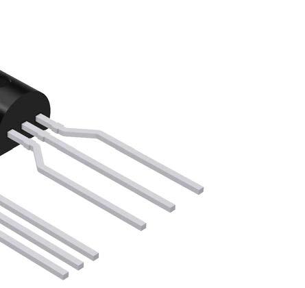
15 SCALE SCALE LP0003A PACKAGE OUTLINE TO mm max height TO EJECTOR PIN OPTIONAL (1.5) TYP 2X 4 MAX SEATING PLANE 3X 12.7 MIN (2.54) NOTE 3 (0.51) TYP 6X MAX SEATING PLANE 2X FORMED LEAD OPTION OTHER DIMENSIONS IDENTICAL TO STRAIGHT LEAD OPTION 3X X STRAIGHT LEAD OPTION 3X X MIN /B 04/2017 NOTES: 1. All linear dimensions are in millimeters. Any dimensions in parenthesis are for reference only. Dimensioning and tolerancing per ASME Y14.5M. 2. This drawing is subject to change without notice. 3. Lead dimensions are not controlled within this area. 4. Reference JEDEC TO-226, variation AA. 5. Shipping method: a. Straight lead option available in bulk pack only. b. Formed lead option available in tape and reel or ammo pack. c. Specific products can be offered in limited combinations of shipping medium and lead options. d. Consult product folder for more information on available options.
16 EXAMPLE BOARD LAYOUT LP0003A TO mm max height TO MAX ALL AROUND TYP (1.07) FULL R TYP METAL TYP 3X ( 0.85) HOLE (1.5) 2X (1.5) 2X METAL (R0.05) TYP SOLDER MASK OPENING (1.27) (2.54) 2X (1.07) 2X SOLDER MASK OPENING LAND PATTERN EXAMPLE STRAIGHT LEAD OPTION NON-SOLDER MASK DEFINED SCALE:15X 0.05 MAX ALL AROUND TYP ( 1.4) 2X ( 1.4) METAL 3X ( 0.9) HOLE METAL (R0.05) TYP SOLDER MASK OPENING (2.6) (5.2) 2X SOLDER MASK OPENING LAND PATTERN EXAMPLE FORMED LEAD OPTION NON-SOLDER MASK DEFINED SCALE:15X /B 04/2017
17 LP0003A TAPE SPECIFICATIONS TO mm max height TO (2.5) TYP 0.5 MIN TYP TYP FOR FORMED LEAD OPTION PACKAGE /B 04/2017
18
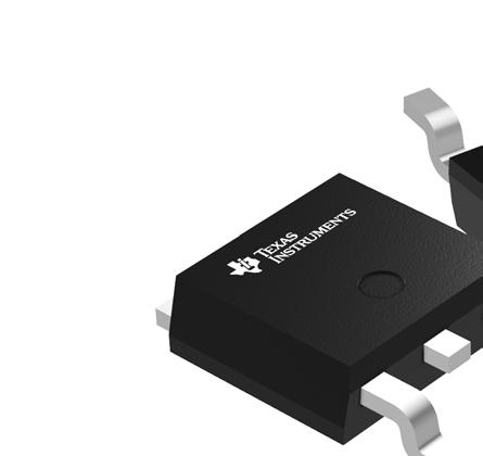
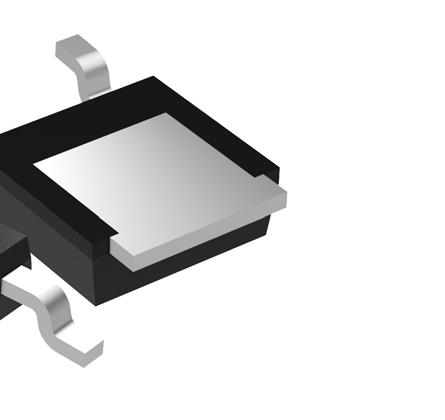
19 SCALE PACKAGE OUTLINE KVU0003A TO mm max height TO B A X C A B OPTIONAL NOTE MAX C SEE DETAIL A 5.21 MIN MIN 1 EXPOSED THERMAL PAD NOTE GAGE PLANE A DETAIL A TYPICAL /A 02/2017 NOTES: 1. All linear dimensions are in millimeters. Any dimensions in parenthesis are for reference only. Dimensioning and tolerancing per ASME Y14.5M. 2. This drawing is subject to change without notice. 3. Shape may vary per different assembly sites. 4. Reference JEDEC registration TO
20 KVU0003A EXAMPLE BOARD LAYOUT TO mm max height TO-252 2X (1) 1 2X (2.75) (6.15) (4.58) 4 SYMM (5.55) 3 (R0.05) TYP (4.2) (2.5) PKG LAND PATTERN EXAMPLE EXPOSED METAL SHOWN SCALE:6X 0.07 MAX ALL AROUND EXPOSED METAL EXPOSED METAL 0.07 MIN ALL AROUND SOLDER MASK OPENING NON SOLDER MASK DEFINED METAL METAL UNDER SOLDER MASK SOLDER MASK DETAILS NOT TO SCALE SOLDER MASK DEFINED SOLDER MASK OPENING NOTES: (continued) /A 02/ This package is designed to be soldered to a thermal pad on the board. For more information, see Texas Instruments literature numbers SLMA002( and SLMA004 ( 6. Vias are optional depending on application, refer to device data sheet. It is recommended that vias under paste be filled, plugged or tented.
21 KVU0003A EXAMPLE STENCIL DESIGN TO mm max height TO-252 (1.18) TYP 2X (1) 1 2X (2.75) (0.14) (1.33) TYP (R0.05) (4.58) 4 SYMM 3 (4.2) 20X (0.98) 20X (1.13) PKG SOLDER PASTE EXAMPLE BASED ON mm THICK STENCIL EXPOSED PAD 65% PRINTED SOLDER COVERAGE BY AREA SCALE:8X /A 02/2017 NOTES: (continued) 7. Laser cutting apertures with trapezoidal walls and rounded corners may offer better paste release. IPC-7525 may have alternate design recommendations. 8. Board assembly site may have different recommendations for stencil design.
22
23
24
25

26 SCALE KCS0003B PACKAGE OUTLINE TO mm max height TO (6.3) ( 3.84) MAX 3X 3.9 MAX X X X /A 10/2015 NOTES: 1. All controlling linear dimensions are in inches. Dimensions in brackets are in millimeters. Any dimension in brackets or parenthesis are for reference only. Dimensioning and tolerancing per ASME Y14.5M. 2. This drawing is subject to change without notice. 3. Reference JEDEC registration TO
27 KCS0003B EXAMPLE BOARD LAYOUT TO mm max height TO MAX ALL AROUND 3X ( 1.2) 2X ( 1.7) METAL 2X SOLDER MASK OPENING (1.7) R ( 0.05) (2.54) 0.07 MAX ALL AROUND SOLDER MASK OPENING (5.08) LAND PATTERN EXAMPLE NON-SOLDER MASK DEFINED SCALE:15X /A 10/2015
28 IMPORTANT NOTICE Texas Instruments Incorporated (TI) reserves the right to make corrections, enhancements, improvements and other changes to its semiconductor products and services per JESD46, latest issue, and to discontinue any product or service per JESD48, latest issue. Buyers should obtain the latest relevant information before placing orders and should verify that such information is current and complete. TI s published terms of sale for semiconductor products ( apply to the sale of packaged integrated circuit products that TI has qualified and released to market. Additional terms may apply to the use or sale of other types of TI products and services. Reproduction of significant portions of TI information in TI data sheets is permissible only if reproduction is without alteration and is accompanied by all associated warranties, conditions, limitations, and notices. TI is not responsible or liable for such reproduced documentation. Information of third parties may be subject to additional restrictions. Resale of TI products or services with statements different from or beyond the parameters stated by TI for that product or service voids all express and any implied warranties for the associated TI product or service and is an unfair and deceptive business practice. TI is not responsible or liable for any such statements. Buyers and others who are developing systems that incorporate TI products (collectively, Designers ) understand and agree that Designers remain responsible for using their independent analysis, evaluation and judgment in designing their applications and that Designers have full and exclusive responsibility to assure the safety of Designers' applications and compliance of their applications (and of all TI products used in or for Designers applications) with all applicable regulations, laws and other applicable requirements. Designer represents that, with respect to their applications, Designer has all the necessary expertise to create and implement safeguards that (1) anticipate dangerous consequences of failures, (2) monitor failures and their consequences, and (3) lessen the likelihood of failures that might cause harm and take appropriate actions. Designer agrees that prior to using or distributing any applications that include TI products, Designer will thoroughly test such applications and the functionality of such TI products as used in such applications. TI s provision of technical, application or other design advice, quality characterization, reliability data or other services or information, including, but not limited to, reference designs and materials relating to evaluation modules, (collectively, TI Resources ) are intended to assist designers who are developing applications that incorporate TI products; by downloading, accessing or using TI Resources in any way, Designer (individually or, if Designer is acting on behalf of a company, Designer s company) agrees to use any particular TI Resource solely for this purpose and subject to the terms of this Notice. TI s provision of TI Resources does not expand or otherwise alter TI s applicable published warranties or warranty disclaimers for TI products, and no additional obligations or liabilities arise from TI providing such TI Resources. TI reserves the right to make corrections, enhancements, improvements and other changes to its TI Resources. TI has not conducted any testing other than that specifically described in the published documentation for a particular TI Resource. Designer is authorized to use, copy and modify any individual TI Resource only in connection with the development of applications that include the TI product(s) identified in such TI Resource. NO OTHER LICENSE, EXPRESS OR IMPLIED, BY ESTOPPEL OR OTHERWISE TO ANY OTHER TI INTELLECTUAL PROPERTY RIGHT, AND NO LICENSE TO ANY TECHNOLOGY OR INTELLECTUAL PROPERTY RIGHT OF TI OR ANY THIRD PARTY IS GRANTED HEREIN, including but not limited to any patent right, copyright, mask work right, or other intellectual property right relating to any combination, machine, or process in which TI products or services are used. Information regarding or referencing third-party products or services does not constitute a license to use such products or services, or a warranty or endorsement thereof. Use of TI Resources may require a license from a third party under the patents or other intellectual property of the third party, or a license from TI under the patents or other intellectual property of TI. TI RESOURCES ARE PROVIDED AS IS AND WITH ALL FAULTS. TI DISCLAIMS ALL OTHER WARRANTIES OR REPRESENTATIONS, EXPRESS OR IMPLIED, REGARDING RESOURCES OR USE THEREOF, INCLUDING BUT NOT LIMITED TO ACCURACY OR COMPLETENESS, TITLE, ANY EPIDEMIC FAILURE WARRANTY AND ANY IMPLIED WARRANTIES OF MERCHANTABILITY, FITNESS FOR A PARTICULAR PURPOSE, AND NON-INFRINGEMENT OF ANY THIRD PARTY INTELLECTUAL PROPERTY RIGHTS. TI SHALL NOT BE LIABLE FOR AND SHALL NOT DEFEND OR INDEMNIFY DESIGNER AGAINST ANY CLAIM, INCLUDING BUT NOT LIMITED TO ANY INFRINGEMENT CLAIM THAT RELATES TO OR IS BASED ON ANY COMBINATION OF PRODUCTS EVEN IF DESCRIBED IN TI RESOURCES OR OTHERWISE. IN NO EVENT SHALL TI BE LIABLE FOR ANY ACTUAL, DIRECT, SPECIAL, COLLATERAL, INDIRECT, PUNITIVE, INCIDENTAL, CONSEQUENTIAL OR EXEMPLARY DAMAGES IN CONNECTION WITH OR ARISING OUT OF TI RESOURCES OR USE THEREOF, AND REGARDLESS OF WHETHER TI HAS BEEN ADVISED OF THE POSSIBILITY OF SUCH DAMAGES. Unless TI has explicitly designated an individual product as meeting the requirements of a particular industry standard (e.g., ISO/TS and ISO 26262), TI is not responsible for any failure to meet such industry standard requirements. Where TI specifically promotes products as facilitating functional safety or as compliant with industry functional safety standards, such products are intended to help enable customers to design and create their own applications that meet applicable functional safety standards and requirements. Using products in an application does not by itself establish any safety features in the application. Designers must ensure compliance with safety-related requirements and standards applicable to their applications. Designer may not use any TI products in life-critical medical equipment unless authorized officers of the parties have executed a special contract specifically governing such use. Life-critical medical equipment is medical equipment where failure of such equipment would cause serious bodily injury or death (e.g., life support, pacemakers, defibrillators, heart pumps, neurostimulators, and implantables). Such equipment includes, without limitation, all medical devices identified by the U.S. Food and Drug Administration as Class III devices and equivalent classifications outside the U.S. TI may expressly designate certain products as completing a particular qualification (e.g., Q100, Military Grade, or Enhanced Product). Designers agree that it has the necessary expertise to select the product with the appropriate qualification designation for their applications and that proper product selection is at Designers own risk. Designers are solely responsible for compliance with all legal and regulatory requirements in connection with such selection. Designer will fully indemnify TI and its representatives against any damages, costs, losses, and/or liabilities arising out of Designer s noncompliance with the terms and provisions of this Notice. Mailing Address: Texas Instruments, Post Office Box , Dallas, Texas Copyright 2017, Texas Instruments Incorporated
description/ordering information
 3-Terminal Regulators Output Current Up To 100 ma No External Components Required Internal Thermal-Overload Protection Internal Short-Circuit Current Limiting Direct Replacement for Industry-Standard MC79L00
TL780 SERIES POSITIVE-VOLTAGE REGULATORS
 FEATURES TL780 SERIES POSITIVE-VOLTAGE REGULATORS SLVS055M APRIL 1981 REVISED OCTOBER 2006 ±1% Output Tolerance at 25 C Internal Short-Circuit Current Limiting ±2% Output Tolerance Over Full Operating
description/ordering information
 µ SLVS060K JUNE 1976 REVISED APRIL 2005 3-Terminal Regulators Output Current Up To 500 ma No External Components High Power-Dissipation Capability Internal Short-Circuit Current Limiting Output Transistor
Data sheet acquired from Harris Semiconductor SCHS038C Revised October 2003
 Data sheet acquired from Harris Semiconductor SCHS038C Revised October 2003 The CD4035B types are supplied in 16-lead hermetic dual-in-line ceramic packages (F3A suffix), 16-lead dual-in-line plastic packages
ORDERING INFORMATION T A PACKAGE ORDERABLE PART NUMBER. SOIC D Tape and reel SN74CBTD3306DR 40 C to85 C
 5-Ω Switch Connection Between Two Ports TTL-Compatible Input Levels Designed to Be Used in Level-Shifting Applications description/ordering information The SN74CBTD3306 features two independent line switches.
Data sheet acquired from Harris Semiconductor SCHS083B Revised March 2003
 Data sheet acquired from Harris Semiconductor SCHS083B Revised March 2003 The CD4536B types are supplied in 16-lead hermetic dual-in-line ceramic packages (F3A suffix), 16-lead dual-in-line plastic packages
description/ordering information
 µ SLVS060K JUNE 1976 REVISED APRIL 2005 3-Terminal Regulators Output Current Up To 500 ma No External Components High Power-Dissipation Capability Internal Short-Circuit Current Limiting Output Transistor
LP324, LP2902 ULTRA-LOW-POWER QUADRUPLE OPERATIONAL AMPLIFIERS
 www.ti.com FEATURES Low Supply Current... 85 µa Typ Low Offset Voltage... 2 mv Typ Low Input Bias Current... 2 na Typ Input Common Mode to GND Wide Supply Voltage... 3 V < V CC < 32 V Pin Compatible With
SN75157 DUAL DIFFERENTIAL LINE RECEIVER
 SN75157 DUAL DIFFERENTIAL LINE RECEIVER Meets or Exceeds the Requirements of ANSI Standards EIA/TIA-422-B and EIA/TIA-423-B and ITU Recommendation V.1 and V.11 Operates From Single 5-V Power Supply Wide
description block diagram
 Fast Transient Response 10-mA to 3-A Load Current Short Circuit Protection Maximum Dropout of 450-mV at 3-A Load Current Separate Bias and VIN Pins Available in Adjustable or Fixed-Output Voltages 5-Pin
GENERAL-PURPOSE LOW-VOLTAGE COMPARATORS
 1 LMV331-Q1 SINGLE, LMV393-Q1 DUAL SLOS468D MAY 2005 REVISED AUGUST 2011 GENERAL-PURPOSE LOW-VOLTAGE COMPARATORS Check for Samples: LMV331-Q1 SINGLE, LMV393-Q1 DUAL 1FEATURES Qualified for Automotive Applications
AVAILABLE OPTIONS PACKAGE SMALL OUTLINE (D) The D package is available taped and reeled. Add the suffix R to the device type (i.e., LT1030CDR).
 The D package is available taped and reeled. Add the suffix R to the device type (i.e., LT1030CDR).") LT1030C QUADRUPLE LOW-POWER LINE DRIVER Low Supply Voltage... ±5 V to ±15 V Supply Current...500 µa Typical Zero Supply Current When Shut Down Outputs Can Be Driven ±30 V Output Open When Off (3-State)
LT1030C QUADRUPLE LOW-POWER LINE DRIVER Low Supply Voltage... ±5 V to ±15 V Supply Current...500 µa Typical Zero Supply Current When Shut Down Outputs Can Be Driven ±30 V Output Open When Off (3-State)
ua9637ac DUAL DIFFERENTIAL LINE RECEIVER
 ua9637ac DUAL DIFFERENTIAL LINE RECEIVER Meets or Exceeds the Requirements of ANSI Standards EIA/TIA-422-B and EIA/TIA-423-B and ITU Recommendations V.10 and V.11 Operates From Single 5-V Power Supply
ORDERING INFORMATION. SOIC DW Tape and reel SN74CBT3384ADWR
 SN74CBT3384A 10-BIT FET BUS SWITCH SCDS004L NOVEMBER 1992 REVISED JANUARY 2004 5-Ω Switch Connection Between Two Ports TTL-Compatible Input Levels description/ordering information The SN74CBT3384A provides
CD54/74AC283, CD54/74ACT283
 Data sheet acquired from Harris Semiconductor SCHS251D August 1998 - Revised May 2000 Features Buffered Inputs Exceeds 2kV ESD Protection MIL-STD-883, Method 3015 SCR-Latchup-Resistant CMOS Process and
SINGLE BUS BUFFER GATE WITH 3-STATE OUTPUT
 1 SN74LVC1G126-Q1 www.ti.com... SCES467B JULY 2003 REVISED APRIL 2008 SINGLE BUS BUFFER GATE WITH 3-STATE OUTPUT 1FEATURES Qualified for Automotive Applications ESD Protection Exceeds 2000 V Per MIL-STD-883,
LF411 JFET-INPUT OPERATIONAL AMPLIFIER
 LF411 JFET-INPUT OPERATIONAL AMPLIFIER Low Input Bias Current, 50 pa Typ Low Input Noise Current, 0.01 pa/ Hz Typ Low Supply Current, 2 ma Typ High Input impedance, 10 12 Ω Typ Low Total Harmonic Distortion
1 to 4 Configurable Clock Buffer for 3D Displays
 1 S3 GND S4 4 5 6 CLKIN 3 CLKOUT3 S1 2 Top View CLKOUT4 S2 1 7 8 9 OE 12 11 10 CLKOUT1 VDD CLKOUT2 CDC1104 SCAS921 SEPTEMBER 2011 1 to 4 Configurable Clock Buffer for 3D Displays Check for Samples: CDC1104
CD74AC251, CD74ACT251
 Data sheet acquired from Harris Semiconductor SCHS246 August 1998 CD74AC251, CD74ACT251 8-Input Multiplexer, Three-State Features Buffered Inputs Typical Propagation Delay - 6ns at V CC = 5V, T A = 25
SN75150 DUAL LINE DRIVER
 SN75150 DUAL LINE DRIVER Meets or Exceeds the Requirement of TIA/EIA-232-F and ITU Recommendation V.28 Withstands Sustained Output Short Circuit to Any Low-Impedance Voltage Between 25 V and 25 V 2-µs
LM2900, LM3900 QUADRUPLE NORTON OPERATIONAL AMPLIFIERS
 LM29, LM39 QUADRUPLE NORTON OPERATIONAL AMPLIFIERS SLOS59 JULY 1979 REVISED SEPTEMBER 199 Wide Range of Supply Voltages, Single or Dual Supplies Wide Bandwidth Large Output Voltage Swing Output Short-Circuit
3.3 V Dual LVTTL to DIfferential LVPECL Translator
 1 SN65LVELT22 www.ti.com... SLLS928 DECEMBER 2008 3.3 V Dual LVTTL to DIfferential LVPECL Translator 1FEATURES 450 ps (typ) Propagation Delay Operating Range: V CC 3.0 V to 3.8 with GND = 0 V
SN74LV04A-Q1 HEX INVERTER
 SN74LV04A-Q1 HEX INVERTER Qualified for Automotive Applications ESD Protection Exceeds 2000 V Per MIL-STD-883, Method 3015; Exceeds 200 V Using Machine Model (C = 200 pf, R = 0) 2-V to 5.5-V Operation
TL750L, TL751L SERIES LOW-DROPOUT VOLTAGE REGULATORS
 TL70L, TL7L SERIES LOW-DROPOUT OLTAGE REGULATORS SLS07P SEPTEMBER 987 REISED FEBRUARY 2003 ery Low Dropout oltage, Less Than 0.6 at 0 ma ery Low Quiescent Current TTL- and CMOS-Compatible Enable on TL7L
74ACT11244 OCTAL BUFFER/LINE DRIVER WITH 3-STATE OUTPUTS
 3-State Outputs Drive Bus Lines or Buffer Memory Address Registers Inputs Are TTL-Voltage Compatible Flow-Through Architecture Optimizes PCB Layout Center-Pin V CC and GND Configurations to Minimize High-Speed
OUTPUT INPUT ADJUSTMENT INPUT INPUT ADJUSTMENT INPUT
 www.ti.com FEATURES LM237, LM337 3-TERMINAL ADJUSTABLE REGULATORS SLVS047I NOVEMBER 1981 REVISED OCTOBER 2006 Output Voltage Range Adjustable From Peak Output Current Constant Over 1.2 V to 37 V Temperature
SN54AC04, SN74AC04 HEX INVERTERS
 SN54AC04, SN74AC04 HEX INVERTERS 2-V to 6-V V CC Operation Inputs Accept Voltages to 6 V Max t pd of 7 ns at 5 V SN54AC04...J OR W PACKAGE SN74AC04...D, DB, N, NS, OR PW PACKAGE (TOP VIEW) 1A 1Y 2A 2Y
Technical Documents. SLPS532A MARCH 2015 REVISED DECEMBER 2017 CSD18536KCS 60 V N-Channel NexFET Power MOSFET
 Product Folder Order Now Technical Documents Tools & Software Support & Community Features Ultra-Low Q g and Q gd Low Thermal Resistance Avalanche Rated Pb-Free Terminal Plating RoHS Compliant Halogen
SN74LVC1G32-Q1 SINGLE 2-INPUT POSITIVE-OR GATE
 FEATURES Qualified for Automotive Applications Customer-Specific Configuration Control Can Be Supported Along With Major-Change Approval Supports 5-V V CC Operation Inputs Accept Voltages to 5.5 V Low
SN75158 DUAL DIFFERENTIAL LINE DRIVER
 SN7558 DUAL DIFFERENTIAL LINE DRIVER Meets or Exceeds the Requirements of ANSI EIA/TIA-422-B and ITU Recommendation V. Single 5-V Supply Balanced-Line Operation TTL Compatible High Output Impedance in
CD74HC4017-Q1 HIGH-SPEED CMOS LOGIC DECADE COUNTER/DIVIDER WITH 10 DECODED OUTPUTS
 Qualified for Automotive Applications Fully Static Operation Buffered Inputs Common Reset Positive Edge Clocking Typical f MAX = 60 MHz at = 5 V, = 5 pf, T A = 25 C Fanout (Over Temperature Range) Standard
SINGLE BUS BUFFER GATE WITH 3-STATE OUTPUT
 1 SN74LVC1G125-Q1... SGES002C APRIL 2003 REVISED APRIL 2008 SINGLE BUS BUFFER GATE WITH 3-STATE OUTPUT 1FEATURES Qualified for Automotive Applications Latch-Up Performance Exceeds 100 ma Per Supports 5-V
High-Side, Bidirectional CURRENT SHUNT MONITOR
 High-Side, Bidirectional CURRENT SHUNT MONITOR SBOS193D MARCH 2001 REVISED JANUARY 200 FEATURES COMPLETE BIDIRECTIONAL CURRENT MEASUREMENT CIRCUIT WIDE SUPPLY RANGE: 2.7V to 0V SUPPLY-INDEPENDENT COMMON-MODE
description/ordering information
 AC Types Feature 1.5-V to 5.5-V Operation and Balanced Noise Immunity at 30% of the Supply Speed of Bipolar F, AS, and S, With Significantly Reduced Power Consumption Balanced Propagation Delays ±24-mA
ORDERING INFORMATION ORDERABLE PART NUMBER SN74CBTS3306PWR
 5-Ω Switch Connection Between Two Ports TTL-Compatible Input Levels description/ordering information The SN74CBTS3306 features independent line switches with Schottky diodes on the I/Os to clamp undershoot.
 PACKAGE OPTION ADDENDUM www.ti.com 17-Mar-2017 PACKAGING INFORMATION Orderable Device Status (1) Package Type Package Drawing Pins Package Qty Eco Plan (2) Lead/Ball Finish (6) MSL Peak Temp (3) Op Temp
PRECISION MICROPOWER SHUNT VOLTAGE REFERENCE
 CATHODE DBZ (SOT-23) PACKAGE (TOP VIEW) ANODE 2 * Pin 3 is attached to substrate and must be connected to ANODE or left open. 3* LM4040-EP SLOS746A SEPTEMBER 20 REVISED SEPTEMBER 20 PRECISION MICROPOWER
ORDERING INFORMATION PACKAGE
 5-Ω Switch Connection Between Two Ports TTL-Compatible Input Levels Designed to Be Used in Level-Shifting Applications description/ordering information The SN74CBTD3861 provides ten bits of high-speed
SN74CBT3861DWR 10-BIT FET BUS SWITCH. description. logic diagram (positive logic)
") SN74CBT3861 10-BIT FET BUS SWITCH SCDS061D APRIL 1998 REVISED OCTOBER 2000 5-Ω Switch Connection Between Two Ports TTL-Compatible Input Levels Latch-Up Performance Exceeds 250 ma Per JESD 17 description
SN74CBT3861 10-BIT FET BUS SWITCH SCDS061D APRIL 1998 REVISED OCTOBER 2000 5-Ω Switch Connection Between Two Ports TTL-Compatible Input Levels Latch-Up Performance Exceeds 250 ma Per JESD 17 description
+5V Precision VOLTAGE REFERENCE
 REF2 REF2 REF2 +V Precision VOLTAGE REFERENCE SBVS3B JANUARY 1993 REVISED JANUARY 2 FEATURES OUTPUT VOLTAGE: +V ±.2% max EXCELLENT TEMPERATURE STABILITY: 1ppm/ C max ( 4 C to +8 C) LOW NOISE: 1µV PP max
PRECISION VOLTAGE REGULATORS
 PRECISION LTAGE REGULATORS 150-mA Load Current Without External Power Transistor Adjustable Current-Limiting Capability Input Voltages up to 40 V Output Adjustable From 2 V to 37 V Direct Replacement for
ORDERING INFORMATION. QFN RGY Tape and reel SN74CBT3257RGYR CU257. SOIC D Tape and reel SN74CBT3257DR
 SN74CBT3257 4-BIT 1-OF-2 FET MULTIPLEXER/DEMULTIPLEXER SCDS017M MAY 1995 REVISED JANUARY 2004 5-Ω Switch Connection Between Two Ports TTL-Compatible Input Levels D, DB, DBQ, OR PW PACKAGE (TOP VIEW) RGY
CD54HC4049, CD74HC4049, CD54HC4050, CD74HC4050
 CD54HC4049, CD74HC4049, CD54HC4050, CD74HC4050 Data sheet acquired from Harris Semiconductor SCHS205I February 1998 - Revised February 2005 High-Speed CMOS Logic Hex Buffers, Inverting and Non-Inverting
CD54/74AC280, CD54/74ACT280
 CD54/74AC280, CD54/74ACT280 Data sheet acquired from Harris Semiconductor SCHS250A August 1998 - Revised May 2000 9-Bit Odd/Even Parity Generator/Checker Features Buffered Inputs Typical Propagation Delay
AVAILABLE OPTIONS PACKAGE VIOmax SMALL OUTLINE. PLASTIC DIP at 25 C (D) (P) 0 C to 70 C 5 mv LM306D LM306P
 (P) 0 C to 70 C 5 mv LM306D LM306P") SLCS8A OCTOBER 979 REVISED OCTOBER 99 Fast Response Times Improved Gain and Accuracy Fanout to Series 5/7 TTL Loads Strobe Capability Short-Circuit and Surge Protection Designed to Be Interchangeable With
SLCS8A OCTOBER 979 REVISED OCTOBER 99 Fast Response Times Improved Gain and Accuracy Fanout to Series 5/7 TTL Loads Strobe Capability Short-Circuit and Surge Protection Designed to Be Interchangeable With
2.5-V INTEGRATED REFERENCE CIRCUIT
 1 1FEATURES Excellent Temperature Stability Wide Operating Current Range Initial Tolerance: 0.2% Max Directly Interchangeable With LM136 Dynamic Impedance: 0.6 Ω Max Needs No Adjustment for Minimum Temperature
SINGLE 2-INPUT POSITIVE-AND GATE
 1 SN74LVC1G08-Q1 www.ti.com... SCES556F MARCH 2004 REVISED APRIL 2008 SINGLE 2-INPUT POSITIVE-AND GATE 1FEATURES Qualified for Automotive Applications Latch-Up Performance Exceeds 100 ma Per Supports 5-V
description/ordering information
 SLVS053D FEBRUARY 1988 REVISED NOVEMBER 2003 Complete PWM Power-Control Function Totem-Pole Outputs for 200-mA Sink or Source Current Output Control Selects Parallel or Push-Pull Operation Internal Circuitry
TL4581 DUAL LOW-NOISE HIGH-DRIVE OPERATIONAL AMPLIFIER
 TL4581 DUAL LOW-NOISE HIGH-DRIVE OPERATIONAL AMPLIFIER SLVS457A JANUARY 2003 REVISED MARCH 2003 Equivalent Input Noise Voltage 5 nv/ Hz Typ at 1 khz Unity-Gain Bandwidth... 10 MHz Typ High Slew Rate...9
LM317M 3-TERMINAL ADJUSTABLE REGULATOR
 FEATURES Output Voltage Range Adjustable From 1.25 V to 37 V Output Current Greater Than 5 ma Internal Short-Circuit Current Limiting Thermal-Overload Protection Output Safe-Area Compensation Q Devices
SN75124 TRIPLE LINE RECEIVER
 SN75124 TRIPLE LINE RECEIER Meets or Exceeds the Requirements of IBM System 360 Input/Output Interface Specification Operates From Single 5- Supply TTL Compatible Built-In Input Threshold Hysteresis High
description/ordering information
 SCAS528D AUGUST 1995 REVISED OCTOBER 2003 2-V to 6-V V CC Operation Inputs Accept Voltages to 6 V Max t pd of 7.5 ns at 5 V SN54AC32...J OR W PACKAGE SN74AC32... D, DB, N, NS, OR PW PACKAGE (TOP VIEW)
TPS76130, TPS76132, TPS76133, TPS76138, TPS76150 LOW-POWER 100-mA LOW-DROPOUT LINEAR REGULATORS
 TPS76130, TPS76132, TPS76133, TPS76138, TPS7610 LOW-POWER 100-mA LOW-DROPOUT LINEAR REGULATORS SLVS178B DECEMBER 1998 REVISED MAY 2001 100-mA Low-Dropout Regulator Fixed Output Voltage Options: V, 3.8
SN75207B DUAL SENSE AMPLIFIER FOR MOS MEMORIES OR DUAL HIGH-SENSITIVITY LINE RECEIVERS
 Plug-In Replacement for SN75107A and SN75107B With Improved Characteristics ± 10-mV Input Sensitivity TTL-Compatible Circuitry Standard Supply Voltages... ±5 V Differential Input Common-Mode Voltage Range
LT , LT MICROPOWER INTEGRATED VOLTAGE REFERENCES
 LT4-.2, LT4-2.5 Initial Accuracy ±4 mv for LT4-.2 ±2 mv for LT4-2.5 Micropower Operation Operates up to 2 ma Very Low Reference Impedance Applications: Portable Meter Reference Portable Test Instruments
5-V Dual Differential PECL Buffer-to-TTL Translator
 1 1FEATURES Dual 5-V Differential PECL-to-TTL Buffer 24-mA TTL Ouputs Operating Range PECL V CC = 4.75 V to 5.25 V with GND = 0 V Support for Clock Frequencies of 250 MHz (TYP) 3.5-ns Typical Propagation
Precision Gain = 10 DIFFERENTIAL AMPLIFIER
 Precision Gain = 0 DIFFERENTIAL AMPLIFIER SBOSA AUGUST 987 REVISED OCTOBER 00 FEATURES ACCURATE GAIN: ±0.0% max HIGH COMMON-MODE REJECTION: 8dB min NONLINEARITY: 0.00% max EASY TO USE PLASTIC 8-PIN DIP,
CD54HC4015, CD74HC4015
 CD54HC4015, CD74HC4015 Data sheet acquired from Harris Semiconductor SCHS198C November 1997 - Revised May 2003 High Speed CMOS Logic Dual 4-Stage Static Shift Register [ /Title (CD74 HC401 5) /Subject
ORDERING INFORMATION. QFN RGY Tape and reel SN74CBT3257RGYR CU257. SOIC D Tape and reel SN74CBT3257DR
 SN74CBT3257 4-BIT 1-OF-2 FET MULTIPLEXER/DEMULTIPLEXER SCDS017M MAY 1995 REVISED JANUARY 2004 5-Ω Switch Connection Between Two Ports TTL-Compatible Input Levels D, DB, DBQ, OR PW PACKAGE (TOP VIEW) RGY
UC1842A-EP, UC1843A-EP, UC1844A-EP, UC1845A-EP CURRENT-MODE PWM CONTROLLER
 Controlled Baseline One Assembly/Test Site, One Fabrication Site Extended Temperature Performance of 55 C to 125 C Enhanced Diminishing Manufacturing Sources (DMS) Support Enhanced Product Change Notification
CD54HC7266, CD74HC7266
 CD54HC7266, CD74HC7266 Data sheet acquired from Harris Semiconductor SCHS219D August 1997 - Revised September 2003 High-Speed CMOS Logic Quad 2-Input EXCLUSIVE NOR Gate [ /Title (CD74H C7266) /Subject
5-V PECL-to-TTL Translator
 1 SN65ELT21 www.ti.com... SLLS923 JUNE 2009 5-V PECL-to-TTL Translator 1FEATURES 3ns (TYP) Propagation Delay Operating Range: V CC = 4.2 V to 5.7 V with GND = 0 V 24-mA TTL Output Deterministic Output
POSITIVE-VOLTAGE REGULATORS
 www.ti.com FEATURES µa78m00 SERIES POSITIVE-VOLTAGE REGULATORS SLVS059P JUNE 1976 REVISED OCTOBER 2005 3-Terminal Regulators High Power-Dissipation Capability Output Current up to 500 ma Internal Short-Circuit
Dual Inverter Gate Check for Samples: SN74LVC2GU04
 1 SN74LVC2GU04 SCES197N APRIL 1999 REVISED DECEMBER 2013 Dual Inverter Gate Check for Samples: SN74LVC2GU04 1FEATURES DESCRIPTION 2 Available in the Texas Instruments NanoFree This dual inverter is designed
description logic diagram (positive logic) logic symbol
 logic symbol") SDAS074B APRIL 1982 REVISED JANUARY 1995 AS1004A Offer High Capacitive-Drive Capability Driver Version of ALS04B and AS04 Package Options Include Plastic Small-Outline (D) Packages, Ceramic Chip Carriers
SDAS074B APRIL 1982 REVISED JANUARY 1995 AS1004A Offer High Capacitive-Drive Capability Driver Version of ALS04B and AS04 Package Options Include Plastic Small-Outline (D) Packages, Ceramic Chip Carriers
SN74AUC1G02 SINGLE 2-INPUT POSITIVE-NOR GATE
 FEATURES SN74AUC1G02 SINGLE 2-INPUT POSITIVE-NOR GATE SCES369P SEPTEMBER 2001 REVISED MARCH 2007 Available in the Texas Instruments Low Power Consumption, 10-µA Max I CC NanoFree Package ±8-mA Output Drive
CD54HC139, CD74HC139, CD54HCT139, CD74HCT139
 Data sheet acquired from Harris Semiconductor SCHS148D September 1997 - Revised October 2003 CD54HC139, CD74HC139, CD54HCT139, CD74HCT139 High-Speed CMOS Logic Dual 2- to 4-Line Decoder/Demultiplexer [
AM26C31-EP QUADRUPLE DIFFERENTIAL LINE DRIVER
 1 1FEATURES Controlled Baseline One Assembly One Test Site One Fabrication Site Extended Temperature Performance of 55 C to 125 C Enhanced Diminishing Manufacturing Sources (DMS) Support Enhanced Product-Change
P-Channel NexFET Power MOSFET
 CSD252W5 www.ti.com SLPS269A JUNE 2 REVISED JULY 2 P-Channel NexFET Power MOSFET Check for Samples: CSD252W5 FEATURES PRODUCT SUMMARY V DS Drain to Drain Voltage 2 V Low Resistance Q g Gate Charge Total
SN75471 THRU SN75473 DUAL PERIPHERAL DRIVERS
 SN747 THRU SN747 DUAL PERIPHERAL DRIVERS SLRS024 DECEMBER 976 REVISED MAY 990 PERIPHERAL DRIVERS FOR HIGH-VOLTAGE HIGH-CURRENT DRIVER APPLICATIONS Characterized for Use to 00 ma High-Voltage Outputs No
CD54HC194, CD74HC194, CD74HCT194
 Data sheet acquired from Harris Semiconductor SCHS164G September 1997 - Revised May 2006 CD54HC194, CD74HC194, CD74HCT194 High-Speed CMOS Logic 4-Bit Bidirectional Universal Shift Register Features Description
SN54ALS09, SN74ALS09 QUADRUPLE 2-INPUT POSITIVE-AND GATES WITH OPEN-COLLECTOR OUTPUTS
 SN54ALS09, SN74ALS09 QUADRUPLE 2-INPUT POSITIVE-AND GATES WITH OPEN-COLLECTOR OUTPUTS SDAS084B APRIL 1982 REVISED DECEMBER 1994 Package Options Include Plastic Small-Outline (D) Packages, Ceramic Chip
ORDERING INFORMATION. QFN RGY Tape and reel SN74CBT3253RGYR CU253. SOIC D Tape and reel SN74CBT3253DR
 SN74CBT3253 DUAL 1-OF-4 FET MULTIPLEXER/DEMULTIPLEXER TTL-Compatible Input Levels D, DB, DBQ, OR PW PACKAGE (TOP VIEW) SCDS018O MAY 1995 REVISED JANUARY 2004 RGY PACKAGE (TOP VIEW) 1OE S1 1B4 1B3 1B2 1B1
description logic diagram (positive logic) logic symbol
 logic symbol") SDAS074B APRIL 1982 REVISED JANUARY 1995 AS1004A Offer High Capacitive-Drive Capability Driver Version of ALS04B and AS04 Package Options Include Plastic Small-Outline (D) Packages, Ceramic Chip Carriers
SDAS074B APRIL 1982 REVISED JANUARY 1995 AS1004A Offer High Capacitive-Drive Capability Driver Version of ALS04B and AS04 Package Options Include Plastic Small-Outline (D) Packages, Ceramic Chip Carriers
DUAL RS-232 DRIVER/RECEIVER WITH IEC PROTECTION
 1 TRS232E www.ti.com... SLLS791C JUNE 2007 REVISED SEPTEMBER 2008 DUAL RS-232 DRIVER/RECEIVER WITH IEC61000-4-2 PROTECTION 1FEATURES 2 Meets or Exceeds TIA/RS-232-F and ITU Recommendation V.28 Operates
±24-mA Output Drive at 3.3 V Operates from 1.65 V to 3.6 V Latch-Up Performance Exceeds 250 ma Per Max t pd of 3.4 ns at 3.
 www.ti.com SN74ALVC245 OCTAL BUS TRANSCEIVER WITH 3-STATE OUTPUTS SCES271D APRIL 1999 REVISED JULY 2004 FEATURES ±24-mA Output Drive at 3.3 V Operates from 1.65 V to 3.6 V Latch-Up Performance Exceeds
SN74LVC2G32-EP DUAL 2-INPUT POSITIVE-OR GATE
 www.ti.com SN74LVC2G32-EP DUAL 2-INPUT POSITIVE-OR GATE SCES543A FEBRUARY 2004 REVISED AUGUST 2006 FEATURES Controlled Baseline Typical V OHV (Output V OH Undershoot) >2 V at V CC = 3.3 V, T A = 25 C One
ORDERING INFORMATION. TOP-SIDE MARKING PDIP N Tube SN74S1051N SN74S1051N
 Designed to Reduce Reflection Noise Repetitive Peak Forward Current to 200 ma 12-Bit Array Structure Suited for Bus-Oriented Systems description/ordering information This Schottky barrier diode bus-termination
CD54HCT258, CD74HCT258 QUADRUPLE 2-LINE TO 1-LINE SELECTORS/MULTIPLEXERS WITH 3-STATE OUTPUTS
 4.5-V to 5.5-V V CC Operation Wide Operating Temperature Range of 55 C to 125 C Balanced Propagation Delays and Transition Times Standard Outputs Drive Up To 10 LS-TTL Loads Significant Power Reduction
SN54ALS38B, SN74ALS38B QUADRUPLE 2-INPUT POSITIVE-NAND BUFFERS WITH OPEN-COLLECTOR OUTPUTS
 SN54ALS38B, SN74ALS38B QUADRUPLE 2-INPUT POSITIVE-NAND BUFFERS WITH OPEN-COLLECTOR OUTPUTS SDAS196B APRIL 1982 REVISED DECEMBER 1994 Package Options Include Plastic Small-Outline (D) Packages, Ceramic
SN74LV374A-Q1 OCTAL EDGE-TRIGGERED D-TYPE FLIP-FLOP WITH 3-STATE OUTPUTS
 Qualified for Automotive Applications Typical V OLP (Output Ground Bounce) 2.3 V at = 3.3 V, T A = 25 C Supports Mixed-Mode Voltage
Supports Partial-Power Down Mode 4.5-V to 5.5-V V Operation. (Output Ground Bounce) <0.8 V at V ESD Protection Exceeds JESD 22
 <0.8 V at V ESD Protection Exceeds JESD 22") www.ti.com FEATURES SN74LV138AT 3-LINE TO 8-LINE DECODER/DEMULTIPLEXER SCLS691 AUGUST 2005 Inputs Are TTL-Voltage Compatible I off Supports Partial-Power Down Mode 4.5-V to 5.5-V V Operation CC Operation
www.ti.com FEATURES SN74LV138AT 3-LINE TO 8-LINE DECODER/DEMULTIPLEXER SCLS691 AUGUST 2005 Inputs Are TTL-Voltage Compatible I off Supports Partial-Power Down Mode 4.5-V to 5.5-V V Operation CC Operation
NOT RECOMMENDED FOR NEW DESIGNS USE CDCVF2510A AS A REPLACEMENT
 CDCVF2510 3.3-V PHASE-LOCK LOOP CLOCK DRIVER FEATURES Designed to Meet and Exceed PC133 SDRAM Registered DIMM Specification Rev. 1.1 Spread Spectrum Clock Compatible Operating Frequency 50 MHz to 175 MHz
ORDERING INFORMATION. TOP-SIDE MARKING PDIP N Tube SN74S1051N SN74S1051N
 Designed to Reduce Reflection Noise Repetitive Peak Forward Current to 200 ma 12-Bit Array Structure Suited for Bus-Oriented Systems description/ordering information This Schottky barrier diode bus-termination
CD74HC4538-Q1 HIGH-SPEED CMOS LOGIC DUAL RETRIGGERABLE PRECISION MONOSTABLE MULTIVIBRATOR
 Qualified for Automotive Applications Retriggerable/Resettable Capability Trigger and Reset Propagation Delays Independent of R X, C X Triggering From the Leading or Trailing Edge Q and Q Buffered Outputs
SN74LVC138A-Q1 3-LINE TO 8-LINE DECODER/DEMULTIPLEXER SCAS708B SEPTEMBER 2003 REVISED FEBRUARY 2008
 1 1FEATURES Qualified for Automotive Applications ESD Protection Exceeds 2000 V Per MIL-STD-883, Method 3015; Exceeds 200 V Using Machine Model (C = 200 pf, R = 0) Operates From 2 V to 3.6 V Inputs Accept
CD54HC283, CD74HC283, CD54HCT283, CD74HCT283
 CD54HC283, CD74HC283, CD54HCT283, CD74HCT283 [ /Title (CD74 HC283, CD74 HCT28 3) /Subject (High Speed CMOS Logic 4-Bit Binary Full Adder Data sheet acquired from Harris Semiconductor SCHS176D November
MC3486 QUADRUPLE DIFFERENTIAL LINE RECEIVER WITH 3-STATE OUTPUTS
 Meets or Exceeds the Requirements of ANSI Standards EIA/TIA-422-B and EIA/TIA-423-B and ITU Recommendations V.10 and V.11 3-State, TTL-Compatible s Fast Transition Times Operates From Single 5-V Supply
CD54HC10, CD74HC10, CD54HCT10, CD74HCT10
 Data sheet acquired from Harris Semiconductor SCHS128C August 1997 - Revised September 2003 CD54HC10, CD74HC10, CD54HCT10, CD74HCT10 High-Speed CMOS Logic Triple 3-Input NAND Gate [ /Title (CD74 HC10,
CD54HC147, CD74HC147, CD74HCT147
 CD54HC147, CD74HC147, CD74HCT147 Data sheet acquired from Harris Semiconductor SCHS149F September 1997 - Revised November 2003 High-Speed CMOS Logic 10- to 4-Line Priority Encoder [ /Title (CD74 HC147,
POSITIVE-VOLTAGE REGULATORS
 µa78l00 SERIES POSITIVE-VOLTAGE REGULATORS SLVS010S JANUARY 1976 REVISED FEBRUARY 2004 3-Terminal Regulators Output Current Up To 100 No External Components Internal Thermal-Overload Protection Internal
description/ordering information
 Wide Operating Voltage Range of 2 V to 6 V Outputs Can Drive Up To 10 LSTTL Loads Low Power Consumption, 80-µA Max I CC Typical t pd = 16 ns ±4-mA Output Drive at 5 V Low Input Current of 1 µa Max Encode
Precision, Gain of 0.2 Level Translation DIFFERENCE AMPLIFIER
 SBOS333B JULY 25 REVISED OCTOBER 25 Precision, Gain of.2 Level Translation DIFFERENCE AMPLIFIER FEATURES GAIN OF.2 TO INTERFACE ±1V SIGNALS TO SINGLE-SUPPLY ADCs GAIN ACCURACY: ±.24% (max) WIDE BANDWIDTH:
VOLTAGE PROTECTION FOR 2-, 3-, OR 4-CELL Lion BATTERIES (2 nd PROTECTION)
") Not Recommended for New Designs: bq900, bq900a, bq90 FEATURES FUNCTION -, -, or -Cell Secondary Protection Each cell in a multiple cell pack is compared to an Low Power Consumption I CC < µa internal reference
Not Recommended for New Designs: bq900, bq900a, bq90 FEATURES FUNCTION -, -, or -Cell Secondary Protection Each cell in a multiple cell pack is compared to an Low Power Consumption I CC < µa internal reference
SN54ALS139, SN74ALS139 DUAL 2-LINE TO 4-LINE DECODERS/DEMULTIPLEXERS
 SN54ALS9, SN74ALS9 DUAL 2-LINE TO 4-LINE DECODERS/DEMULTIPLEXERS Designed Specifically for High-Speed Memory Decoders and Data Transmission Systems Incorporate Two Enable Inputs to Simplify Cascading and/or
SN74LVC1G08-EP SINGLE 2-INPUT POSITIVE-AND GATE
 SN74LVC1G08-EP SINGLE 2-INPUT POSITIVE-AND GATE SCES454C DECEMBER 2003 REVISED AUGUST 2006 FEATURES Controlled Baseline I off Supports Partial-Power-Down Mode One Assembly/Test Site, One Fabrication Operation
30V, N-Channel NexFET Power MOSFETs
 CSD755Q5A www.ti.com SLPS3A DECEMBER 2 REVISED JULY 2 3V, N-Channel NexFET Power MOSFETs Check for Samples: CSD755Q5A FEATURES PRODUCT SUMMARY T A = 25 C unless otherwise stated TYPICAL VALUE UNIT 2 Ultralow
Dual Voltage Detector with Adjustable Hysteresis
 TPS3806J20 Dual Voltage Detector with Adjustable Hysteresis SLVS393A JULY 2001 REVISED NOVEMBER 2004 FEATURES DESCRIPTION Dual Voltage Detector With Adjustable The TPS3806 integrates two independent voltage
CD54HC280, CD74HC280, CD54HCT280, CD74HCT280
 Data sheet acquired from Harris Semiconductor SCHS175D November 1997 - Revised October 2003 Features CD54HC280, CD74HC280, CD54HCT280, CD74HCT280 High-Speed CMOS Logic 9-Bit Odd/Even Parity Generator/Checker
SN74LVC1G14-EP SINGLE SCHMITT-TRIGGER INVERTER SCES674 MARCH 2007
 1 SN74LVC1G14-EP SINGLE SCHMITT-TRIGGER INVERTER SCES674 MARCH 2007 1FEATURES Controlled Baseline JESD 78, Class II One Assembly/Test Site, One Fabrication ESD Protection Exceeds JESD 22 Site 2000-V Human-Body