KCT College OF ENGG AND TECH. VILLAGE FATEHGARH DISTT.SANGRUR
|
|
|
- Merry George
- 6 years ago
- Views:
Transcription

1 Department of Electrical Engineering LAB MANUAL ELECTRONIC CIRCUITS LAB B.Tech IV Semester KCT College OF ENGG AND TECH. VILLAGE FATEHGARH DISTT.SANGRUR
2 INDEX Sr. No.. 2. Experiment Name Realization of logic gates using NAND and NOR gates. Verification of truth table for D flip flop. 3. Verification of truth table for IC flip flops (D Latch, D flip flop, JK flip flops). 4. Verification of truth table for Asynchronous 4 bit decade counter using IC To study different waveforms of clippers & clampers 6. Measurement of Parameters of Emitter Follower and Source Follower; RI, AV, AI &Ro. 7. To obtain the frequency response of an amplifier and calculate the gain bandwidth of the amplifier. 8. To study the Class B and Class AB amplifier. 9. To study the characteristics symmetry amplifier.. To design and set up an RC phase shift oscillator using BJT and to observe the sinusoidal. Application of Op-Amp(74) as inverting and non-inverting amplifier. 2. Application of OP-AMP as Schmitt Trigger.. 3. Design the monostable multivibrator using the IC To study the application of IC555 as an Astable multivibrator. 5. To study the operation of Arithmetic Logic Unit IC To study about logic gates and verify their truth tables.
3 EXPERIMENT- NAND AND NOR GATES Aim: Realization of logic gates using NAND and NOR gates. Apparatus :. Fixed output regulated power supply of 5V. 2. Two logic & two logic inputs with output provided on Sockets. 3. Red output indicators is provided on the front panel to observe the output status. 4. Four NAND & Four NOR gates are printed on the front panel, IC s placed inside the cabinet & connections for input & output are brought out on socket. Theory: To build logic circuit, OR gate is used for addition sign, AND gate is used for multiplication sign & NOT gate is used for inverse sign. Hence AND OR NOT logic gates are basic building blocks logic circuits. NAND gates & NOR gates can be used to build AND, OR, NOT gates. Hence NAND gates & NOR gates are called universal building block of logic gates. Procedure: Verification of NAND as AND gate. Connect A & B inputs of AND gate to logic inputs & as shown in the truth table for AND gate to logic indicator. 2. Switch ON the instrument using ON/OFF Toggle switch provided on the front panel. 3. Check the output indicator. If it glows the indication is that the output is in the state & if it does not glow the indication is that output is in state. 4. Similarly verify the input for other combination of input A & B as shown in the truth cable. 2
4 Verification of NOR as other gates 3
5 RESULT:NAND gate and NOR gate as other gates are verified. EXPERIMENT-2 TRUTH TABLE FOR D FLIP FLOP Aim: Verification of truth table for D flip flop. Apparatus Required:. Fixed output regulated power supply of 5V. 2. Hz Mono shot clock pulse with pulsar switch is provided on the front panel. 3. One logic inputs logic & logic selectable using SPDT switches are provided on the front panel. 4. Two red output indicators are also provided on the front panel 5. IC 742 is mounted on the front panel,7 important connections are brought out on sockets. Theory: A flip flop is an electronic circuit that has two stable states, one representing a binary & the other binary.if one put into one state, the flip flop will remain in that state as long 4
6 as power is applied or until it is changed. In digital circuits flip flops are used in variety of storage, counting, sequencing & timing applications. The D flip flop has two outputs that determine whether it is storing a binary & the other binary. It also has two inputs. These are called D and T and work differently. The data or bit to be stored is applied to the D input. The T input line controls the flip flop. it is used to determine whether the input data at D is to be recognized or ignored. if the T input is high, the data on the D line get stored in the flip flop. If the T line is low the D input line data has no effect and bit stored previously is retained. Procedure:. Connect the output of logic inputs to D input of the flip flop. Also connect Q outputs to the output indicator. 2. Connect Hz clock output to the clock input of the flip flop. 3. Switch ON the instrument using ON/OFF toggle switch provided on the front panel. 4. Verify the truth table of input combinations. Observation Table: INPUTS CLOCK(CK) OUTPUTS D Q Q' 5
7 Result: The truth tables for NOR gate latch is verified. 6
8 EXPERIMENT-3 IC FLIP FLOPS (D LATCH, D FLIP FLOP, JK FLIP FLOPS) Aim: Verification of truth table for IC flip flops (D Latch, D flip flop, JK flip flops). Apparatus:. D type flip flop using TTL IC JK flip flop using TTL IC D latch using IC Fixed output DC regulated Power Supply of 5V. 5. Hz monoshot clock pulse with pulser switch. 6. Four logic inputs logic & logic selectable using SPDT switches. 7. Two red output indicators. 8. IC 74, 7474 & Single and double patch cards. Theory: A flip flop is electronic circuit that has two stable states, one representing a binary and the other binary. In digital circuits, flip flops are used in a variety of storage, counting, sequencing and timing applications. There are three basic types of flip flops, the set-reset (also known as R-S flip flop or a latch), the D type and the JK. The RS flip flop is the simplest. The D flip flop has two outputs that determine whether it is storing a binary or a binary. It also has two inputs. There are called D and T and work differently. The JK flip flop is the most versatile binary storage element. It can perform all the functions of R, S and D flip flops plus it can do several other things. An integrated circuit JK flip flop is really two RS flip flops in one. These are called Master and Slave. Both flip flops are controlled by a common clock pulse to the T input. Procedure: Verification of D Latch:. Connect the output of NOT Gate to R input through patchcord. Connect 3 logic inputs to Preset (PR), Clear (CR) & D input of the flip-flop as shown in fig. through patchcords. Also connect Q & Q outputs to output indicators. 7
9 2. Connect Hz clock output to Clock (CK) input of the flip flop. Verification of JK Flip Flop: 8
10 . Connect the 4 Logic inputs to Preset (PR), Clear (CR), J & K input of the Flip-Flop as shown in fig. through patchcords. Also connect Q & Q outputs to output indicators. 2. Connect Hz clock output to Clock (CK) input of the flip flop. 3. Switch ON the instrument using ON/ OFF toggle switch provided on the front panel. 4. Verify the Truth Table for various sets of input combinations. Verification of D Type Flip Flop:. Connect the 3 Logic inputs to Preset (PR), Clear (CR) & D input of the Flip-Flop as shown in fig. through patchcords. Also connect Q & Q outputs to output indicators. 2. Connect Hz clock output to Clock (CK) input of the flip flop. 3. Switch ON the instrument using ON/ OFF toggle switch provided on the front panel. 9
11 4. Verify the Truth Table for various sets of input combinations. Result: The truth tables for D Latch, D flip flop, JK flip flops are verified.
12 EXPERIMENT-4 ASYNCHRONOUS 4 BIT DECADE COUNTER USING IC 749 Aim: Verification of truth table for Asynchronous 4 bit decade counter using IC 749. Apparatus:. Fixed output DC regulated power supply 5V DC. 2. Monoshot clock pulse of Hz, seven single point patch cords for connection. 3. Four output logic indicator. 4. IC 7476 is placed inside & connections are brought out on sockets. Theory: 4 bit ripple counter counts upto 5 & then resets to. But it can be made to reset to at any clock pulse. For this purpose we operate the reset connections automatically using 4 input NAND gate. as you know that output of a NAND gate is low if & only if all the inputs are high.suppose we want to convert 4-bit forward counter to decade counter.for Decade counter it is required that counter should count up to 9 & than resets to zero at tenth clock pulse. We know that at a tenth clock pulse output of 2 nd & 4th flip flop is high & output of st & 3rd flip flop is low. So we choose Q output of 2nd & 4th flip flop & Q` output of st & 3rd flip flop for the nputs for the inputs of 4-input NAND gate. Also Connect output of NAND gate to common reset pin of all the flip flops. As you can program the counter for any number of pulses that is why this counter is known as Modulo Counter. Circuit Diagram:
13 CLOCK QD QC QB QA Procedure:. Connect the circuit as shown. Through patch cords i.e. connect clock output to ck (clock pulse) input of first flip flop, connect Q output of first flip flop to ck input of second flip flop, Q output of second flip flop to ck input of third flip flop, Q output of third flip flop 2
14 to ck input of fourth flip flop as shown. Also connect all the all four Q outputs to output indicators Connect the Q` output of first flip flop, Q` output of second flip flop, Q output of third flip flop, Q output of fourth flip flop to the inputs of NAND gate. 2. Keep all the J & K inputs open, as in open condition they assume to be in state. 3. Switch ON the instrument using ON/OFF toggle switch provided on the front panel. 4. For counting, apply clock pulses one by one using pulser switch. Note down all the four outputs at the application of each pulse & verify the truth table. Result: The truth table of Asynchronous 4 bit decade counter is verified. 3
15 EXPERIMENT-5 CLIPPERS & CLAMPERS Aim :- To study different waveforms of clippers & clampers. Appartus :-Function Generator( MHz), CRO(3 MHz), probes, Connecting Wires, Diode IN47, Resistor KΩ, Capacitor.μf. Clippers It is frequently necessary to modify the shape of various waveforms for use in instrumentation, controls, computation, and communications. Wave shaping is often achieved by relatively simple combination of diodes, resistors, and voltage sources. Such circuits are called clippers, limiters, amplitude selectors, or slicers. Clipper circuits are primarily used to prevent a waveform from exceeding a particular limit, either positive or negative. For example, one may need to limit a power supply s output voltage so it does not exceed +5 V. The most widely used wave shaping circuit is the rectifier, which you have previously studied. Fig. shows a positive clipper circuit. Circuit Diagram :- Fig. A positive clipper circuit: (a) Sinusoidal input to clipper circuit; (b) A positive clipper circuit; (c) Output of ideal positive clipper and (d) Output of actual positive clipper circuit As indicated, the output voltage has the entire positive half-cycles clipped off. The circuit works as follows: During the positive half-cycle of the input voltage, the diode turns on. For an ideal 4
16 diode, the output voltage is zero. For an actual diode the output voltage is equal to Vγ, the cut-in voltage of the diode. During the negative half-cycle, the diode is reverse-biased and can be approximated by an open circuit. In many clippers, the load resistor, RL, is much larger than the series resistor, R. In which case, essentially all of the negative half-cycle voltage appears at the output through voltage-divider action. If RL and R are comparable, then on the negative halfcycle, the output voltage would be given by Vo = Vp = Vp (RL / (RL + R)). Since the first Vγ volts are used to begin conduction in the diode, the output signal is clipped near Vγ, rather than at V. If the diode polarity is reversed, the result is a negative clipper that removes the negative half cycle. In this case, the clipping levels occur near -Vγ. Clampers In certain instances, it may be desirable to keep the output waveform essentially unchanged, but modify its dc level to some required value. This can be done by the use of diodes, resistors, capacitors, and voltage sources. Such circuits are known as clampers. For example, if the input voltage signal swings from -V to +V, a positive dc clamper can produce an output that keeps the signal wave shape intact but swings the voltage from V to +2V. TV receivers use a dc clamper to add a dc voltage to the video signal. Here the dc clamper is usually called a dc restorer. In Figure a positive dc clamper is shown. The clamper operates as follows: During the negative half-cycle of the input voltage, the diode turns on as illustrated in Figure. At the negative peak, the capacitor charges up to Vp with the polarity shown and the output voltage iszero. As the voltage grows beyond the negative peak, the diode shuts off as shown in Fig. Fig:- Positive dc clamper: (a) Sinusoidal input to positive dc clamper; (b) Positive dc clamper; and (c) Clamped sinusoidal output The capacitor retains the voltage for a short time. The RLC time constant is deliberately made much larger than the period, T, of the input signal. Hence, the capacitor remains almost fully charged during the entire off time of the diode. The capacitor thus acts like a battery of Vp volts and now only passes the ac signal, which rides on top of VP. The output voltage signal, therefore, consists of the input signal riding on a dc voltage of +Vp volts. Since the diode drops Vγ volts when conducting, the capacitor voltage does not quite reach +Vp volts. For this reason, the dc clamping is not perfect, and the negative peaks are at -Vγ as shown in Fig. When the polarity of the diode in Fig. is reversed, the polarity of the capacitor voltage reverses also, and the circuit becomes a negative dc clamper. Ideally, the output voltage consists of the input voltage riding on a dc voltage of -Vp volts. If the diode is considered nonideal, then the output will consist of the input signal riding on a dc voltage of -(Vp-Vγ) volts, and the positive peaks will occur at Vγ volts. 5
17 Fig: Positive clamping circuit operation From the above discussions, it can be seen that when the diode points upward, a positive dc clamper results. When the diode points downward, the circuit is a negative dc clamper. The clamping value can be modified by putting a voltage source V B in series with the diode, shifting the peak voltage to (± Vγ ± VB), depending on the sign of VB and the polarity of the diode. Results. Ideal Clipping Circuits Build 4 circuits a. Vin = 8VP-P, khz, VB = & 2V. b. Sketch the input and output waveforms. c. Record the voltage at which clipping occurs. 2. Series-Biased Clippers Build 4 circuits a. Vsin = 8VP-P, khz, VB = & 2V. b. Sketch the input and output waveforms. c. Record the voltage at which clipping occurs. 6
18 3. Parallel-Biased Clipper Build circuit a. Vin = 8VP-P, khz, VB and VB2 = 2V. b. Sketch the input and output waveforms. c. Record the voltage at which clipping occurs. 4. Clamper Build circuit a. Vin = 8VP-P, khz, Vdc = 2V. b. Sketch the input and output waveforms. 7
19 EXPERIMENT-6 Aim: Measurement of Parameters of Emitter Follower and Source Follower; RI, AV, AI &Ro. Apparatus: FETBFW, Transistor BC7, Resistors, Capacitors, CRO, Function Generator, Multi meter. CIRCUIT DIAGRAM: 8
20 THEORY: EMITTER FOLLOWER The common collector circuit is also known as emitter follower. The ac output voltage from a CC circuit is essentially the same as the input voltage; there is no voltage gain or phase shift. Thus, the CC circuit can be said to have a voltage gain of. The fact that the CC output voltage follows the changes in signal voltage gives the circuit its other name emitter follower. The input impedance of a CC amplifier is high. Output impedance is low and the Voltage gain is almost unity. Because of these Characteristics the CC circuit is normally used as a buffer amplifier, placed between a high impedance signal source and a low impedance load. SOURCE FOLLOWER The FET common drain circuit has the output voltage developed across the source resistor Rs. Here the ac output voltage is closely equal to the ac input voltage, and the circuit can be said to have unity gain. Because the output voltage at the source terminal follows the signal voltage at the gate, the common drain circuit is also known as a source follower. A common drain circuit has a voltage gain approximately equal to, no phase shift between input and output, very high input impedance and low output impedance. Because of its high Zi, low Zo and unity gain the CD circuit is used as a buffer amplifier between a high impedance signal source and a low impedance load. PROCEDURE:. Connect the circuit as per the circuit diagram. 2. Apply Vslv KHz signal from the signal generator. 3. Observe corresponding output from the CRO and then calculate voltage gain using the formula Av=Vo/Vi. 4. Measure voltage across AB terminals and then calculate input current by using the formula Iin=Vab/Rab. 5. Measure current flowing through resistor at Source (or Emitter) terminal and note down it as Iout. 6. Calculate Current gain using the formula AI=Iin/I out. 7. Calculate input resistance using the formula Rin=Vin/Iin. 8. To calculate the output resistance, connect the pot at the output and vary the resistance of the pot up to half of the output with RL is equal to infinity. The resistance of pot is the output resistance. PRECAUTIONS:. Wires should be checked for good continuity 2. FET terminals must be identified and connected carefully. 9
21 EXPERIMENT-7 Aim :- To obtain the frequency response of an amplifier and calculate the gain bandwidth of the amplifier. Apparatus:- Transistor BC7, Resistors, Capacitors, CRO, Signal generator. Circuit Diagram :- Theory:The CE amplifier is a small signal amplifier. This small signal amplifier accepts low voltage ac inputs and produces amplified outputs. A single stage BJT circuit may be employed as a small signal amplifier; has two cascaded stages give much more amplification. Designing for a particular voltage gain requires the use of a ac negative feedback to stabilize the gain. For good bias stability, the emitter resistor voltage drop should be much larger than the base -emitter voltage. And Re resistor will provide the required negative feedback to the circuit. CE is provided to provide necessary gain to the circuit. Allbypass capacitors should be selected to have the smallest possible capacitance value, both to minimize the physical size of the circuit for economy. The coupling capacitors should have a negligible effect on the frequency response of the circuit. Procedure:. Connect the circuit as per the circuit diagram. 2. Give lhz signal and 2mv p-p as Vs from the signal generator 3. Observe the output on CRO and note down the output voltage. 4. Keeping input voltage constant and by varying the frequency in steps Hz-MHz, note down the corresponding output voltages. 5. Calculate gain in db and plot the frequency response on semi log sheet 2
22 TABULAR FORM:- Input voltage (Vi)= NO. FREQUENCY OUTPUT VOLTAGE(Vo) GAIN Av=Vo/Vi Model Graph:- Precautions:. Wires should be checked for good continuity. 2. Transistor terminals must be identified and connected carefully. 2 GAIN IN db 2 log gain
23 22
24 EXPERIMENT-8 Aim :- To study the Class B and Class AB amplifier. Apparatus: Digital multimeter (Fluke 8A, BK PRECISION 283B). Function Generator Wavetek FG3B. Digital oscilloscope Tektronix TDS 2. MJE8 NPN and MJE7 PNP Darlington transistors. N448 diodes 3. C=47 uf 2; C=47uF. R=8.2 uf / 2W. Procedure:. You are provided with two heat sinks, which should be attached to the transistors during the lab exercise. The heat sink supposed to be electrically insulated from the collector of the transistor, however it is always recommended to avoid any contact of the heat sinks to the ground or to each other. Occasionally check the temperature of the heat sink, if you cannot keep your finger of the heat sink for more than twenty seconds the transistors may be too hot. Shut the power off and check your circuit. 2. Connect the class B power amplifier shown in Fig. using MJE8 NPN and MJE7 PNP Darlington transistors instead of single BJTs. Use the RL= 8.2 Ω resistor to replace the loudspeaker s load. 3. Use a dual voltage Power Supply and connect its POS terminal as Vcc, NEG terminal as Vee and COM terminal as a common ground. Set the power supply voltage to 6V DC. Measure the DC quiescent point values. Compare the voltages and currents from simulation with the experimental data in a Table 2.. If your results are significantly different (more than 5%) from your simulated values, try to find out and eliminate the reason for that discrepancy. 4. Once you are satisfied that your circuit is biased correctly, then connect the signal generator to the input. Set the signal generator to a frequency of khz. For the input signal level of Vin = 3Vrms (~4Vp) sketch the output voltage across the 8.2 Ω load on top of your MicroCap simulation plot. Compare the simulated and experimental waveforms and explain the differences if any. 5. Increase the input sinusoidal voltage until you notice a clipping in the output voltage. Record this value and compare with DC power supply voltages. For these readings you can use the BK Precision meter to measure the AC input current (it measures the RMS value), measure the input voltage after the digital meter (scope) as it is shown in Figure

25 6. For the input signal Vin= 2 Vrms and Vin=.8Vrms calculate the input AC power P in, the output AC power Po, the DC input power from the DC supply P DC. Also calculate the AC voltage gain AV [db], the AC power gain [db] and the amplifier efficiency of the class B power amplifier. Circuit Diagram:- IB Vin FG + Vcc IC + ON _ C Q IE _ Vo RL OFF + Q2 _ Vee a) Positive half cycle operation b) Class B output waveforms Fig. Class B power amplifier operation Power Amplifier Class B Class B amplification involves using a dual voltage power supply along with two power transistors, an NPN, and its complementary PNP device. Such a circuit is shown in Fig. and its operation could be explained as following: In the absence of an input signal, neither transistor conducts; both transistors are off. On the positive half of the input cycle, once the input signal is greater than.7 V, Q will turn on and current flows as shown in Fig. Notice that the base-emitter voltage of Q causes Q2 to be held in the off state since Q2 s base-emitter is reverse biased. As the input signal swings into the negative half of its cycle and exceeds.7v, Q2 is turned on and its base-emitter voltage reverse biases the base-emitter junction of Q, turning it off. Typical output waveforms for both Q and Q2 BJTs and a Class B amplifier output are shown in Fig. The time required for the input signal to move from zero volts to +.7 V or to -.7 V is the time during which conduction does not occur, consequently the output sits at zero 24
 Quiescent Current, and hence low standing power dissipation and optimum power efficiency.")
26 volts for this interval, producing what is called crossover distortion. Crossover distortion takes its name from the dead-time distortion occurring when the input crosses over from -.7 V to +.7 V or from +.7 V to -.7 V. Class B has a very low (almost zero) Quiescent Current, and hence low standing power dissipation and optimum power efficiency. However it should be clear that in practice Class B may suffer from problems when handling low-level signals. In the absence of an input signal, a Class B power amplifier should have zero volts dc on the output terminal with respect to ground, if the transistors are well matched. Often, they are not well matched, so the student should be aware that it is quite possible to have a dc voltage present at the output. Some output loads, such as speakers, may be damaged by dc. If such loads are to be used, they must be capacitively coupled to the output in order to block the dc. Power Amplifier Class AB Crossover distortion could be eliminated in class AB power amplifiers by the addition of the diode circuitry shown in Fig. Vcc C Vin FG ID C2 R Q D Vo RL D2 Q2 R2 Vee a) Class AB circuit diagram b) Class AB output waveforms Fig. Class AB power amplifier circuit Since the diodes in Fig. are on all the time, both Q and Q2 are held at the edge of the conduction mode by the diode voltages (A small but controlled Quiescent Current). When the input goes either positive or negative, very little voltage is required to put Q or Q2 into full conduction. Typical output waveforms for both Q and Q2 BJTs and a Class AB amplifier output are shown in Fig. V AV [db] 2 log o..() Vin AP [db] log 25 Po Pin..(2)
27 2 2V PDC VDCIDC VDC Io p VDC OP RL POAC V ( rms ) VO ( P ) O RL 2 RL..(3) Po AC PDC..(4)...(5)
28 EXPERIMENT -9 Aim:- To study the characteristics symmetry amplifier. Apparatus:-.Transistor CL, BC558, 2. Resistor 4.7k_,5k_ 2, 3. Capacitor μf 2 4. Diode IN Signal Generator (-3)MHz 6. CRO 3MHz 7. Regulated power supply (-3)V 8. Bread Board Circuit Diagram:- Formula: Theory:- Input power, Pin=2VccIm/П Output power, Pout=VmIm/2 Power Gain or efficiency, η=л/4(vm/vcc) A power amplifier is said to be Class B amplifier if the Q-point and the input signal are selected such that the output signal is obtained only for one half cycle for a full input cycle. The Q-point is selected on the X-axis. Hence, the transistor remains in the active region only for the positive half of the input signal. There are two types of Class B power amplifiers: Push Pull amplifier and complementary symmetry amplifier. In the complementary symmetry amplifier, one n-p-n and another p-np transistor is used. The matched pair of transistor are used in the common collector configuration. In the positive half cycle of the input signal, the n-p-n transistor is driven into active region and starts conducting and in negative half cycle, the p-n-p transistor is driven into conduction. However there is a period between the crossing of the half cycles of the input signals, for which none of the transistor is active and output, is zero. OBSERVATION 27
29 CALCULATION OUTPUT SIGNAL: AMPLITUDE : TIME PERIOD : POWER, PIN = 2VCC Im/л OUTPUT POWER, POUT = VmIm/2 EFFICIENCY, η = ( л/4)( Vm/ VCC) x Procedure:-. Connections are given as per the circuit diagram without diodes. 2. Observe the waveforms and note the amplitude and time period of the input signal and distorted waveforms. 3. Connections are made with diodes. 4. Observe the waveforms and note the amplitude and time period of the input signal and output signal. 5. Draw the waveforms for the readings. 6. Calculate the maximum output power and efficiency. Hence the nature of the output signal gets distorted and no longer remains the same as the input. This distortion is called cross-over distortion. Due to this distortion, each transistor conducts for less than half cycle rather than the complete half cycle. To overcomethis distortion, we add 2 diodes to provide a fixed bias and eliminate cross-over distortion. Result:- 28
30 29
31 EXPERIMENT- Aim:- To design and set up an RC phase shift oscillator using BJT and to observe the sinusoidal output waveform. Apparatus:- Transistor, dc source,capacitors, resistors, potentiometer, breadboard and CRO. Circuit Diagram:- Theory: An oscillator is an electronic circuit for generating an ac signal voltage with a dc supply as the only input requirement. The frequency of the generated signal is decided by the circuit elements. An oscillator requires an amplifier, a frequency selective network, and a positive feedback from the output to the input. The Barkhausen criterion for sustained oscillation is A_ = where A is the gain of the amplifier and is the feedback factor. The unity gain means signal is in phase. (If the signal is 8 out of phase, gain will be.). If a common emitter amplifier is used, with a resistive collector load, there is a 8 phase shift between the voltages at the base and the collector. In the figure shown, three sections of phase shift networks are used so that each section introduces approximately 6_ phase shift at resonant frequency. By analysis, resonant frequency f can be expressed by the equation:- 3
32 Procedure:. Connections are made as per circuit diagram. 2. Connect CRO output terminals and observe the waveform. 3. Calculate practically the frequency of oscillations by using the expression f = / T. 4. Repeat the above steps 2,3 for different values of L, and note down the practically values of oscillations of the RC-phase shift oscillator. Precautions:. All the connections should be correct. 2. Transistor terminals must be identified properly. 3. Reading should be taken without any parallax error. 3
33 Experiment- Aim:- Application of Op-Amp(74) as inverting and non-inverting amplifier. Apparatus: Function Generator CRO Dual RPS Op-Amp Bread Board Resistors Connecting wires and probes 3 MHz 3 MHz 3 V IC 74 As required As required Theory:- The input signal Vi is applied to the inverting input terminal through R and the non-inverting input terminal of the op-amp is grounded. The output voltage V o is fed back to the inverting input terminal through the R f - R network, where Rf is the feedback resistor. The output voltage is given as, Vo = - ACL Vi Here the negative sign indicates that the output voltage is 8 signal. out of phase with the input Procedure :. Connections are given as per the circuit diagram Vcc and - Vcc supply is given to the power supply terminal of the Op-Amp IC. 3. By adjusting the amplitude and frequency knobs of the function generator, appropriate input voltage is applied to the inverting input terminal of the Op-Amp. 4. The output voltage is obtained in the CRO and the input and output voltage waveforms are plotted in a graph sheet. 32
34 PIN DIAGRAM: CIRCUIT DIAGRAM OF INVERTING AMPLIFIER: 33
35 DESIGN: We know for an inverting Amplifier ACL = RF / R Assume R ( approx. KΩ ) and find Rf Hence Vo = - ACL Vi 34
36 OBSERVATIONS: S.No. 2. Input Amplitude ( No. of div x Volts per div ) Time period ( No. of div x Time per div ) Output Practical Theoretical RESULT: The design and testing of the inverting amplifier is done and the input and output waveforms were drawn. 35
37 36
38 Experiment-2 AIM:- NON - INVERTING AMPLIFIER:Apparatus:- S.No Name of the Apparatus Function Generator CRO Dual RPS Op-Amp Bread Board Resistors Connecting wires and probes 3 MHz 3 MHz 3 V IC 74 Range As required As required Quantity THEORY: The input signal Vi is applied to the non - inverting input terminal of the op-amp. This circuit amplifies the signal without inverting the input signal. It is also called negative feedback system since the output is feedback to the inverting input terminals. The differential voltage Vd at the inverting input terminal of the op-amp is zero ideally and the output voltage is given as, Vo = ACL Vi Here the output voltage is in phase with the input signal. PROCEDURE:. Connections are given as per the circuit diagram Vcc and - Vcc supply is given to the power supply terminal of the Op-Amp IC. 3. By adjusting the amplitude and frequency knobs of the function generator, appropriate input voltage is applied to the non - inverting input terminal of the Op-Amp. 4. The output voltage is obtained in the CRO and the input and output voltage waveforms are plotted in a graph sheet. PIN DIAGRAM: 37
39 CIRCUIT DIAGRAM OF NON INVERITNG AMPLIFIER: DESIGN: We know for a Non-inverting Amplifier ACL = + ( RF / R) Assume R ( approx. KΩ ) and find Rf Hence Vo = ACL Vi OBSERVATIONS: S.No. 2. Input Amplitude ( No. of div x Volts per div ) Time period ( No. of div x Time per div ) Output Practical Theoretical RESULT: The design and testing of the Non-inverting amplifier is done and the input and output waveforms were drawn. 38
40 Experiment-3 Aim:- Application of OP-AMP as Schmitt Trigger. Apparatus:- S.NO 2 ITEM OP-AMP RESISTOR RANGE IC74 K, 2.2K Q.TY CRO RPS DUAL(-3) V CIRCUIT DIAGRAM:- +Vcc=+2 V 2.2kΩ 2 3 F.G Vin = 4 V F = KHz 7 IC Vcc= - 2 V Vo R2=2.2k Ω + R= Ω Pin Diagram: 39
41 Offset Null 8 No connection Inverting 2 Non-Inverting 3 6 Output -Vee 4 5 Offset Null IC Vcc O/P wave form: Vo (v) t THEORY: Schmitt trigger is useful in squaring of slowly varying i/p waveforms.vin is applied to inverting terminal of op-amp.feedback voltage is applied to the non-inverting terminal. LTP is the point at which output changes from high level to low level.this is highly useful in triangular waveform generation, wave shape pulse generator, A/D convertor etc. PROCEDURE : The connections are made as shown in the circuit diagram.the signal which has to be made square is applied to the inverting terminal. Here the i/p is a sine waveform.the supply voltage is switched ON and the o/p waveform is recorded through CRO.The UTP and LTP are also found and the theoretical and practical values are verified. LTP = R/ ( R + R2 ) X(-Vsat) UTP = R2 /( R + R2 ) X( +Vsat) Design : +Vsat= +Vcc=5v -Vsat= -Vee= -5v RESULT: The Schmitt trigger circuit is connected and the waveforms are drawn and theoretical and practical values for the trip points are verified. 4
42 Theoretical values = Practical values = 4
43 EXPERIMENT-4 Aim :- Design the monostable multivibrator using the IC555. Apparatus :S.NO 2 ITEM IC RESISTOR RANGE NE555 9K Q.TY 3 CAPACITOR 4 5 RPS CRO. F. F (-3) V - THEORY: A monostable multivibrator has one stable state and a quasistable state. When it is triggered by an external agency it switches from the stable state to quasistable state and returns back to stable state. The time during which it states in quasistable state is determined from the time constant RC. When it is triggered by a continuous pulse it generates a square wave. Monostable multi vibrator can be realized by a pair of regeneratively coupled active devices, resistance devices and op-amps. DESIGN : T =.ms C =. F T =.96RC R = T /.96C R 9 K Circuit Diagram 42 = (.* -3) / (.96*.*-6) = 9.2 K
44 PIN DIAGRAM:- PROCEDURE: The connections are made as per the diagram. The value of R is chosen as 9k. The DCB is set to the designed value. The power supply is switched on and set to +5V. The output of the pulse generator is set to the desired frequency. Here the frequency of triggering should be greater than width of ON period (i.e.) T >W. The output is observed using CRO and the result is compared with the theoretical value. The experiment can be repeated for different values of C and the results are tabulated. OBSERVATION:- C (uf) Theoritical(T=.95 RC(ms))) 43 Practical T(ms)
45 RESULT: Thus the monostable multivibrator using IC555 is designed and its output waveform is traced `EXPERIMENT-5 APPLICATION OF IC555 AS AN ASTABLE MULTIVIBRATOR. Aim: To study the application of IC555 as an Astable multivibrator. Apparatus:- S.NO ITEM IC RANGE NE555 2 RESISTOR K, 2.2K 3 CAPACITOR. F. F 4 CRO - 5 RPS DUAL(-3) V Q.TY Theory: The IC555 timer is a 8 pin IC that can be connected to external components for astable operation. The simplified block diagram is drawn. The OP-AMP has threshold and control inputs. Whenever the threshold voltage exceeds the control voltage, the high output from the OP AMP will set the flip-flop. The collector of discharge transistor goes to pin 7. When this pin is connected to an external trimming capacitor, a high Q output from the flip flop will saturate the transistor and discharge the capacitor. When Q is low the transistor opens and the capacitor charges. The complementary signal out of the flip-flop goes to pin 3 and output. When external reset pin is grounded it inhibits the device. The on off feature is useful in many application. The lower OP- AMP inverting terminal input is called the trigger because of the voltage divider. The noninverting input has a voltage of +Vcc/3, the OP-Amp output goes high and resets the flip flop. Circuit diagram: 44
46 PIN DIAGRAM:- Procedure : The connections are made as per the circuit diagram and the values of R and C are calculated assuming anyone term and they are settled. The output waveform is noted down and graph is drawn and also the theoretical and practical time period is verified. Observation: C (uf) Theoretical time period(us) 45 Practical time Theoretical freq Practical period(us) (khz) freq(khz)
47 Calculation: Theoretical: T =.69(Ra+Rb)C=.69(* *3)*.*-6) =.22 s Practical: T = Ton + Toff MODEL GRAPH: Result : Thus the astable multivibrator circuit using IC555 is constructed and verified its theoretical and practical time period. 46
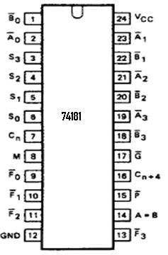
48 EXPERIMENT-6 Aim:- To study the operation of Arithmetic Logic Unit IC 748. Apparatus:- IC 748, etc. Pin detail & Function table:- Pin Detail :- 47
49 48
50 49
51 AIM: To study about logic gates and verify their truth tables. APPARATUS REQUIRED: SL No COMPONENT SPECIFICATION QTY AND GATE IC 748 OR GATE IC 7432 NOT GATE IC 744 NAND GATE 2 I/P IC 74 NOR GATE IC 742 X-OR GATE IC 7486 NAND GATE 3 I/P IC 74 IC TRAINER KIT PATCH CORD 4 THEORY: Circuit that takes the logical decision and the process are called logic gates. Each gate has one or more input and only one output. OR, AND and NOT are basic gates. NAND, NOR and X-OR are known as universal gates. Basic gates form these gates. AND GATE: The AND gate performs a logical multiplication commonly known as AND function. The output is high when both the inputs are high. The output is low level when any one of the inputs is low. OR GATE: THE OR GATE PERFORMS A LOGICAL ADDITION COMMONLY KNOWN AS OR FUNCTION. THE OUTPUT IS HIGH WHEN ANY ONE OF THE INPUTS IS HIGH. THE OUTPUT IS LOW LEVEL WHEN BOTH THE INPUTS ARE LOW. 5
52 NOT GATE: The NOT gate is called an inverter. The output is high when the input is low. The output is low when the input is high. NAND GATE: The NAND gate is a contraction of AND-NOT. The output is high when both inputs are low and any one of the input is low.the output is low level when both inputs are high. NOR GATE: The NOR gate is a contraction of OR-NOT. The output is high when both inputs are low. The output is low when one or both inputs are high. X-OR GATE: The output is high when any one of the inputs is high. The output is low when both the inputs are low and both the inputs are high. PROCEDURE: (i) Connections are given as per circuit diagram. (ii) Logical inputs are given as per circuit diagram. (iii) Observe the output and verify the truth table. 5
53 AND GATE: SYMBOL: OR GATE: 52 PIN DIAGRAM:
54 NOT GATE: SYMBOL: 53 PIN DIAGRAM:
55 X-OR GATE : SYMBOL : 2-INPUT NAND GATE: 54 PIN DIAGRAM :
56 SYMBOL: 3-INPUT NAND GATE : 55 PIN DIAGRAM:
57 NOR GATE: 56
Dev Bhoomi Institute Of Technology Department of Electronics and Communication Engineering PRACTICAL INSTRUCTION SHEET
 Dev Bhoomi Institute Of Technology Department of Electronics and Communication Engineering PRACTICAL INSTRUCTION SHEET LABORATORY MANUAL EXPERIMENT NO. ISSUE NO. : ISSUE DATE: REV. NO. : REV. DATE : PAGE:
 RAJALAKSHMI ENGINEERING COLLEGE THANDALAM 602 105. DEPARTMENT OF ECE LAB MANUAL CLASS : II YEAR ECE SEMESTER : IV SEM (DEC 2009) SUBJECT CODE : EC2258 SUBJECT : LINEAR INTEGRATED CIRCUITS LAB PREPARED
Document Name: Electronic Circuits Lab. Facebook: Twitter:
 Document Name: Electronic Circuits Lab www.vidyathiplus.in Facebook: www.facebook.com/vidyarthiplus Twitter: www.twitter.com/vidyarthiplus Copyright 2011-2015 Vidyarthiplus.in (VP Group) Page 1 CIRCUIT
B.E. SEMESTER III (ELECTRICAL) SUBJECT CODE: X30902 Subject Name: Analog & Digital Electronics
 SUBJECT CODE: X30902 Subject Name: Analog & Digital Electronics") B.E. SEMESTER III (ELECTRICAL) SUBJECT CODE: X30902 Subject Name: Analog & Digital Electronics Sr. No. Date TITLE To From Marks Sign 1 To verify the application of op-amp as an Inverting Amplifier 2 To
B.E. SEMESTER III (ELECTRICAL) SUBJECT CODE: X30902 Subject Name: Analog & Digital Electronics Sr. No. Date TITLE To From Marks Sign 1 To verify the application of op-amp as an Inverting Amplifier 2 To
Analog Electronic Circuits Lab-manual
 2014 Analog Electronic Circuits Lab-manual Prof. Dr Tahir Izhar University of Engineering & Technology LAHORE 1/09/2014 Contents Experiment-1:...4 Learning to use the multimeter for checking and indentifying
Dev Bhoomi Institute Of Technology Department of Electronics and Communication Engineering PRACTICAL INSTRUCTION SHEET REV. NO. : REV.
 Dev Bhoomi Institute Of Technology Department of Electronics and Communication Engineering PRACTICAL INSTRUCTION SHEET LABORATORY MANUAL EXPERIMENT NO. ISSUE NO. : ISSUE DATE: July 200 REV. NO. : REV.
1. LINEAR WAVE SHAPING
 Aim: 1. LINEAR WAVE SHAPING i) To design a low pass RC circuit for the given cutoff frequency and obtain its frequency response. ii) To observe the response of the designed low pass RC circuit for the
Government Polytechnic Muzaffarpur Name of the Lab: Applied Electronics Lab
 Government Polytechnic Muzaffarpur Name of the Lab: Applied Electronics Lab Subject Code: 1620408 Experiment-1 Aim: To obtain the characteristics of field effect transistor (FET). Theory: The Field Effect
HIGH LOW Astable multivibrators HIGH LOW 1:1
 1. Multivibrators A multivibrator circuit oscillates between a HIGH state and a LOW state producing a continuous output. Astable multivibrators generally have an even 50% duty cycle, that is that 50% of
R & D Electronics DIGITAL IC TRAINER. Model : DE-150. Feature: Object: Specification:
 DIGITAL IC TRAINER Model : DE-150 Object: To Study the Operation of Digital Logic ICs TTL and CMOS. To Study the All Gates, Flip-Flops, Counters etc. To Study the both the basic and advance digital electronics
EXPERIMENT 2.2 NON-LINEAR OP-AMP CIRCUITS
 2.16 EXPERIMENT 2.2 NONLINEAR OPAMP CIRCUITS 2.2.1 OBJECTIVE a. To study the operation of 741 opamp as comparator. b. To study the operation of active diode circuits (precisions circuits) using opamps,
ANALOG ELECTRONIC CIRCUITS LABORATORY MANUAL (CODE: EEE - 228)
") ANALOG ELECTRONIC CIRCUITS LABORATORY MANUAL (CODE: EEE - 228) DEPARTMENT OF ELECTRONICS & COMMUNICATION ENGINEERING ANIL NEERUKONDA INSTITUTE OF TECHNOLOGY & SCIENCES (Affiliated to AU, Approved by AICTE
ANALOG ELECTRONIC CIRCUITS LABORATORY MANUAL (CODE: EEE - 228) DEPARTMENT OF ELECTRONICS & COMMUNICATION ENGINEERING ANIL NEERUKONDA INSTITUTE OF TECHNOLOGY & SCIENCES (Affiliated to AU, Approved by AICTE
LIC & COMMUNICATION LAB MANUAL
 LIC & Communication Lab Manual LIC & COMMUNICATION LAB MANUAL FOR V SEMESTER B.E (E& ( E&C) (For private circulation only) NAME: DEPARTMENT OF ELECTRONICS & COMMUNICATION SRI SIDDHARTHA INSTITUTE OF TECHNOLOGY
ASTABLE MULTIVIBRATOR
 555 TIMER ASTABLE MULTIIBRATOR MONOSTABLE MULTIIBRATOR 555 TIMER PHYSICS (LAB MANUAL) PHYSICS (LAB MANUAL) 555 TIMER Introduction The 555 timer is an integrated circuit (chip) implementing a variety of
THIRD SEMESTER ELECTRONICS - II BASIC ELECTRICAL & ELECTRONICS LAB DEPARTMENT OF ELECTRICAL ENGINEERING
 THIRD SEMESTER ELECTRONICS - II BASIC ELECTRICAL & ELECTRONICS LAB DEPARTMENT OF ELECTRICAL ENGINEERING Prepared By: Checked By: Approved By: Engr. Saqib Riaz Engr. M.Nasim Khan Dr.Noman Jafri Lecturer
 11. What is fall time (tf) in transistor? The time required for the collector current to fall from 90% to 10% of its DEPARTMENT OF ECE EC 6401 Electronic Circuits II UNIT-IV WAVE SHAPING AND MULTIVIBRATOR
Facility of Engineering. Biomedical Engineering Department. Medical Electronic Lab BME (317) Post-lab Forms
 Post-lab Forms") Facility of Engineering Biomedical Engineering Department Medical Electronic Lab BME (317) Post-lab Forms Prepared by Eng.Hala Amari Spring 2014 Facility of Engineering Biomedical Engineering Department
Facility of Engineering Biomedical Engineering Department Medical Electronic Lab BME (317) Post-lab Forms Prepared by Eng.Hala Amari Spring 2014 Facility of Engineering Biomedical Engineering Department
Gechstudentszone.wordpress.com
 8.1 Operational Amplifier (Op-Amp) UNIT 8: Operational Amplifier An operational amplifier ("op-amp") is a DC-coupled high-gain electronic voltage amplifier with a differential input and, usually, a single-ended
Shankersinh Vaghela Bapu Institute of Technology INDEX
 Shankersinh Vaghela Bapu Institute of Technology Diploma EE Semester III 3330905: ELECTRONIC COMPONENTS AND CIRCUITS INDEX Sr. No. Title Page Date Sign Grade 1 Obtain I-V characteristic of Diode. 2 To
GATE SOLVED PAPER - IN
 YEAR 202 ONE MARK Q. The i-v characteristics of the diode in the circuit given below are : v -. A v 0.7 V i 500 07 $ = * 0 A, v < 0.7 V The current in the circuit is (A) 0 ma (C) 6.67 ma (B) 9.3 ma (D)
 EC 6411 CIRCUITS AND SIMULATION INTEGRATED LABORATORY LABORATORY MANUAL INDEX EXPT.NO NAME OF THE EXPERIMENT PAGE NO 1 HALF WAVE AND FULL WAVE RECTIFIER 3 2 FIXED BIAS AMPLIFIER CIRCUIT USING BJT 3 BJT
Summer 2015 Examination
 Summer 2015 Examination Subject Code: 17445 Model Answer Important Instructions to examiners: 1) The answers should be examined by key words and not as word-to-word as given in the model answer scheme.
GOVERNMENT OF KARNATAKA KARNATAKA STATE PRE-UNIVERSITY EDUCATION EXAMINATION BOARD II YEAR PUC EXAMINATION JULY-2012 SCHEME OF VALUATION
 GOVERNMENT OF KARNATAKA KARNATAKA STATE PRE-UNIVERSITY EDUCATION EXAMINATION BOARD II YEAR PUC EXAMINATION JULY-0 SCHEME OF VALUATION Subject Code: 40 Subject: PART - A 0. Which region of the transistor
Process Components. Process component
 What are PROCESS COMPONENTS? Input Transducer Process component Output Transducer The input transducer circuits are connected to PROCESS COMPONENTS. These components control the action of the OUTPUT components
Analog Circuit II Laboratory ( EC 409) EC 409 Analog Electronics Lab - II
 EC 409 Analog Electronics Lab - II") Analog Circuit II Laboratory ( EC 409) Subject Subject Title L T P Contact Credit Full Code Hours / Unit# Marks EC 409 Analog Electronics Lab - II 0 0 2 2 1 100 Course Outcomes:- After successful completion
Analog Circuit II Laboratory ( EC 409) Subject Subject Title L T P Contact Credit Full Code Hours / Unit# Marks EC 409 Analog Electronics Lab - II 0 0 2 2 1 100 Course Outcomes:- After successful completion
i Intelligent Digitize Emulated Achievement Lab
 Electronics Circuits Equipment Intelligent Digitize Emulated Achievement Lab intelligent digitize emulated achievement lab is a digitized-based training system, which utilizes integrated Hardware Platform,
EXPT NO: 1.A. COMMON EMITTER AMPLIFIER (Software) PRELAB:
 PRELAB:") EXPT NO: 1.A COMMON EMITTER AMPLIFIER (Software) PRELAB: 1. Study the operation and working principle of CE amplifier. 2. Identify all the formulae you will need in this Lab. 3. Study the procedure of
EXPT NO: 1.A COMMON EMITTER AMPLIFIER (Software) PRELAB: 1. Study the operation and working principle of CE amplifier. 2. Identify all the formulae you will need in this Lab. 3. Study the procedure of
Multivibrators. Department of Electrical & Electronics Engineering, Amrita School of Engineering
 Multivibrators Multivibrators Multivibrator is an electronic circuit that generates square, rectangular, pulse waveforms. Also called as nonlinear oscillators or function generators. Multivibrator is basically
GOVERNMENT OF KARNATAKA KARNATAKA STATE PRE-UNIVERSITY EDUCATION EXAMINATION BOARD II YEAR PUC EXAMINATION MARCH-2012 SCHEME OF VALUATION
 GOVERNMENT OF KARNATAKA KARNATAKA STATE PRE-UNIVERSITY EDUCATION EXAMINATION BOARD II YEAR PUC EXAMINATION MARCH-0 SCHEME OF VALUATION Subject Code: 0 Subject: Qn. PART - A 0. Which is the largest of three
DEPARTMENT OF ELECTRICAL & ELECTRONICS ENGINEERING
 DEPARTMENT OF ELECTRICAL & ELECTRONICS ENGINEERING (Regulation 2013) EE 6311 LINEAR AND DIGITAL INTEGRATED CIRCUITS LAB MANUAL 1 SYLLABUS OBJECTIVES: Working Practice in simulators / CAD Tools / Experiment
Lab 4 : Transistor Oscillators
 Objective: Lab 4 : Transistor Oscillators In this lab, you will learn how to design and implement a colpitts oscillator. In part II you will implement a RC phase shift oscillator Hardware Required : Pre
UNIT - 1 OPERATIONAL AMPLIFIER FUNDAMENTALS
 UNIT - 1 OPERATIONAL AMPLIFIER FUNDAMENTALS 1.1 Basic operational amplifier circuit- hte basic circuit of an operational amplifier is as shown in above fig. has a differential amplifier input stage and
For input: Peak to peak amplitude of the input = volts. Time period for 1 full cycle = sec
 Inverting amplifier: [Closed Loop Configuration] Design: A CL = V o /V in = - R f / R in ; Assume R in = ; Gain = ; Circuit Diagram: RF +10V F.G ~ + Rin 2 3 7 IC741 + 4 6 v0-10v CRO Model Graph Inverting
ELECTRONIC CIRCUITS LAB
 ELECTRONIC CIRCUITS LAB 1 2 STATE INSTITUTE OF TECHNICAL TEACHERS TRAINING AND RESEARCH GENERAL INSTRUCTIONS Rough record and Fair record are needed to record the experiments conducted in the laboratory.
the reactance of the capacitor, 1/2πfC, is equal to the resistance at a frequency of 4 to 5 khz.
 EXPERIMENT 12 INTRODUCTION TO PSPICE AND AC VOLTAGE DIVIDERS OBJECTIVE To gain familiarity with PSPICE, and to review in greater detail the ac voltage dividers studied in Experiment 14. PROCEDURE 1) Connect
Practical Manual. Deptt.of Electronics &Communication Engg. (ECE)
") Practical Manual LAB: BASICS OF ELECTRONICS 1 ST SEM.(CSE/CV) Deptt.of Electronics &Communication Engg. (ECE) RAO PAHALD SINGH GROUP OF INSTITUTIONS BALANA(MOHINDER GARH)12302 Prepared By. Mr.SANDEEP KUMAR
Practical Manual LAB: BASICS OF ELECTRONICS 1 ST SEM.(CSE/CV) Deptt.of Electronics &Communication Engg. (ECE) RAO PAHALD SINGH GROUP OF INSTITUTIONS BALANA(MOHINDER GARH)12302 Prepared By. Mr.SANDEEP KUMAR
hij Teacher Resource Bank GCE Electronics Exemplar Examination Questions ELEC2 Further Electronics
 hij Teacher Resource Bank GCE Electronics Exemplar Examination Questions ELEC2 Further Electronics The Assessment and Qualifications Alliance (AQA) is a company limited by guarantee registered in England
CIRCUIT DIAGRAM Half Wave Rectifier. Half Wave Rectifier with filter 2012/ODD/III/ECE/EC I/LM 1
 CIRCUIT DIAGRAM Half Wave Rectifier Half Wave Rectifier with filter 2012/ODD/III/ECE/EC I/LM 1 Ex.No. 1 Date: / /2012 Power supply circuit using Half Wave rectifiers AIM To Build and understand the operation
LINEAR IC APPLICATIONS
 1 B.Tech III Year I Semester (R09) Regular & Supplementary Examinations December/January 2013/14 1 (a) Why is R e in an emitter-coupled differential amplifier replaced by a constant current source? (b)
Dev Bhoomi Institute Of Technology Department of Electronics and Communication Engineering PRACTICAL INSTRUCTION SHEET REV. NO. : REV.
 Dev Bhoomi Institute Of Technology Department of Electronics and Communication Engineering PRACTICAL INSTRUCTION SHEET LABORATORY MANUAL EXPERIMENT NO. 1 ISSUE NO. : ISSUE DATE: July 2010 REV. NO. : REV.
Operating Manual Ver.1.1
 Multivibrators (Astable and Monostable) Operating Manual Ver.1.1 An ISO 9001 : 2000 company 94-101, Electronic Complex Pardesipura, Indore- 452010, India Tel : 91-731- 2570301/02, 4211100 Fax: 91-731-
Analog Electronics Laboratory
 Circuit Diagram a) Center tap FWR without filter b) Center tap FWR with C filter AC Supply AC Supply D2 c) Bridge Rectifier without filter d) Bridge Rectifier with C filter AC Supply AC Supply Waveforms
DEPARTMENT OF ELECTRICAL ENGINEERING LAB WORK EE301 ELECTRONIC CIRCUITS
 DEPARTMENT OF ELECTRICAL ENGINEERING LAB WORK EE301 ELECTRONIC CIRCUITS EXPERIMENT : 4 TITLE : 555 TIMERS OUTCOME : Upon completion of this unit, the student should be able to: 1. gain experience with
GOVERNMENT OF KARNATAKA KARNATAKA STATE PRE-UNIVERSITY EDUCATION EXAMINATION BOARD II YEAR PUC EXAMINATION MARCH-2013 SCHEME OF VALUATION
 GOVERNMENT OF KARNATAKA KARNATAKA STATE PRE-UNIVERSITY EDUCATION EXAMINATION BOARD II YEAR PUC EXAMINATION MARCH-03 SCHEME OF VALUATION Subject Code: 0 Subject: PART - A 0. What does the arrow mark indicate
G.H. Raisoni College of Engineering, Nagpur. Department of Information Technology 1
 1 2 List of Experiment CYCLE I 1) To plot the frequency response for inverting configuration of OP AMP on breadboard. 2) To plot the frequency response for non inverting configuration of OP AMP on breadboard.
ST.ANNE S COLLEGE OF ENGINEERING AND TECHNOLOGY ANGUCHETTYPALAYAM, PANRUTI Department of Electronics & Communication Engineering OBSERVATION
 ST.ANNE S COLLEGE OF ENGINEERING AND TECHNOLOGY ANGUCHETTYPALAYAM, PANRUTI 67 Department of Electronics & Communication Engineering OBSERVATION EC836 ANALOG AND DIGITAL CIRCUITS LABORATORY STUDENT NAME
Lab 2 Revisited Exercise
 Lab 2 Revisited Exercise +15V 100k 1K 2N2222 Wire up led display Note the ground leads LED orientation 6.091 IAP 2008 Lecture 3 1 Comparator, Oscillator +5 +15 1k 2 V- 7 6 Vin 3 V+ 4 V o Notice that power
Exam Booklet. Pulse Circuits
 Exam Booklet Pulse Circuits Pulse Circuits STUDY ASSIGNMENT This booklet contains two examinations for the six lessons entitled Pulse Circuits. The material is intended to provide the last training sought
CONTENTS Sl. No. Experiment Page No
 CONTENTS Sl. No. Experiment Page No 1a Given a 4-variable logic expression, simplify it using Entered Variable Map and realize the simplified logic expression using 8:1 multiplexer IC. 2a 3a 4a 5a 6a 1b
State the application of negative feedback and positive feedback (one in each case)
") (ISO/IEC - 700-005 Certified) Subject Code: 073 Model wer Page No: / N Important Instructions to examiners: ) The answers should be examined by key words and not as word-to-word as given in the model answer
(ISO/IEC - 700-005 Certified) Subject Code: 073 Model wer Page No: / N Important Instructions to examiners: ) The answers should be examined by key words and not as word-to-word as given in the model answer
Electronic Devices. Floyd. Chapter 7. Ninth Edition. Electronic Devices, 9th edition Thomas L. Floyd
 Electronic Devices Ninth Edition Floyd Chapter 7 Power Amplifiers A power amplifier is a large signal amplifier that produces a replica of the input signal on its output. In the case shown here, the output
Rectifiers and Filters
 Experiment No. : 1 Rectifiers and Filters Date: / / Aim : To design and testing of Full wave centre tapped transformer type and Bridge type rectifier circuits with and without Capacitor filter. Determination
GATE: Electronics MCQs (Practice Test 1 of 13)
") GATE: Electronics MCQs (Practice Test 1 of 13) 1. Removing bypass capacitor across the emitter leg resistor in a CE amplifier causes a. increase in current gain b. decrease in current gain c. increase
GATE: Electronics MCQs (Practice Test 1 of 13) 1. Removing bypass capacitor across the emitter leg resistor in a CE amplifier causes a. increase in current gain b. decrease in current gain c. increase
Linear electronic. Lecture No. 1
 1 Lecture No. 1 2 3 4 5 Lecture No. 2 6 7 8 9 10 11 Lecture No. 3 12 13 14 Lecture No. 4 Example: find Frequency response analysis for the circuit shown in figure below. Where R S =4kR B1 =8kR B2 =4k R
 SET - 1 1. a) Write the application of attenuator b) State the clamping theorem c) Write the application of Monostable multi vibrator d) Draw the diagram for Diode two input AND gate e) Define the terms
CRO AIM:- To study the use of Cathode Ray Oscilloscope (CRO).
.") 1. 1 To study CRO. CRO AIM:- To study the use of Cathode Ray Oscilloscope (CRO). Apparatus: - C.R.O, Connecting probe (BNC cable). Theory:An CRO is easily the most useful instrument available for testing
1. 1 To study CRO. CRO AIM:- To study the use of Cathode Ray Oscilloscope (CRO). Apparatus: - C.R.O, Connecting probe (BNC cable). Theory:An CRO is easily the most useful instrument available for testing
Facility of Engineering. Biomedical Engineering Department. Medical Electronic Lab BME (317) Pre-Report Forms
 Pre-Report Forms") Facility of Engineering Biomedical Engineering Department Medical Electronic Lab BME (317) Pre-Report Forms Prepared by Eng.Hala Amari Spring 2014 Facility of Engineering Biomedical Engineering Department
Facility of Engineering Biomedical Engineering Department Medical Electronic Lab BME (317) Pre-Report Forms Prepared by Eng.Hala Amari Spring 2014 Facility of Engineering Biomedical Engineering Department
INTEGRATED CIRCUITS AND APPLICATIONS LAB MANUAL
 INTEGRATED CIRCUITS AND APPLICATIONS LAB MANUAL V SEMESTER Department of Electronics and communication Engineering Government Engineering College, Dahod-389151 http://www.gecdahod.ac.in/ L A B M A N U
OBJECTIVE TYPE QUESTIONS
 OBJECTIVE TYPE QUESTIONS Q.1 The breakdown mechanism in a lightly doped p-n junction under reverse biased condition is called (A) avalanche breakdown. (B) zener breakdown. (C) breakdown by tunnelling.
Logic Gates & Training Boards
 Logic Gates & Training Boards ANALOG TO DIGITAL (A/D) CONVERTOR (ELP.112.140) Objective : To study Analog to Digital & Digital to Analog convertors using R-2R network & Successive Approximation Method.
Shankersinh Vaghela Bapu Institute of Technology
 Shankersinh Vaghela Bapu Institute of Technology B.E. Semester III (EC) 131101: Basic Electronics INDEX Sr. No. Title Page Date Sign Grade 1 [A] To Study the V-I characteristic of PN junction diode. [B]
ELECTRONIC CIRCUITS. Time: Three Hours Maximum Marks: 100
 EC 40 MODEL TEST PAPER - 1 ELECTRONIC CIRCUITS Time: Three Hours Maximum Marks: 100 Answer five questions, taking ANY TWO from Group A, any two from Group B and all from Group C. All parts of a question
LABORATORY EXPERIMENTS DIGITAL COMMUNICATION
 LABORATORY EXPERIMENTS DIGITAL COMMUNICATION INDEX S. No. Name of the Program 1 Study of Pulse Amplitude Modulation (PAM) and Demodulation. 2 Study of Pulse Width Modulation (PWM) and Demodulation. 3 Study
POWER ELECTRONICS LAB MANUAL
 JIS College of Engineering (An Autonomous Institution) Department of Electrical Engineering POWER ELECTRONICS LAB MANUAL Exp-1. Study of characteristics of an SCR AIM: To obtain the V-I characteristics
Physics 309 Lab 3 Bipolar junction transistor
 Physics 39 Lab 3 Bipolar junction transistor The purpose of this third lab is to learn the principles of operation of a bipolar junction transistor, how to characterize its performances, and how to use
Crystal Oscillator. Circuit symbol
 Crystal Oscillator Crystal Oscillator Piezoelectric crystal (quartz) Operates as a resonant circuit Shows great stability in oscillation frequency Piezoelectric effect : When mechanical stress is applied
PESIT BANGALORE SOUTH CAMPUS BASIC ELECTRONICS
 PESIT BANGALORE SOUTH CAMPUS QUESTION BANK BASIC ELECTRONICS Sub Code: 17ELN15 / 17ELN25 IA Marks: 20 Hrs/ Week: 04 Exam Marks: 80 Total Hours: 50 Exam Hours: 03 Name of Faculty: Mr. Udoshi Basavaraj Module
CHADALAWADA RAMANAMMA ENGINEERING COLLEGE (AUTONOMOUS) Chadalawada Nagar, Renigunta Road, Tirupati
 Chadalawada Nagar, Renigunta Road, Tirupati") ELECTRONIC DEVICES AND CIRCUITS LABORATORY MANUAL Subject Code : 17CA04305 Regulations : R17 Class : III Semester (ECE) CHADALAWADA RAMANAMMA ENGINEERING COLLEGE (AUTONOMOUS) Chadalawada Nagar, Renigunta
ELECTRONIC DEVICES AND CIRCUITS LABORATORY MANUAL Subject Code : 17CA04305 Regulations : R17 Class : III Semester (ECE) CHADALAWADA RAMANAMMA ENGINEERING COLLEGE (AUTONOMOUS) Chadalawada Nagar, Renigunta
Difference between BJTs and FETs. Junction Field Effect Transistors (JFET)
") Difference between BJTs and FETs Transistors can be categorized according to their structure, and two of the more commonly known transistor structures, are the BJT and FET. The comparison between BJTs
Difference between BJTs and FETs Transistors can be categorized according to their structure, and two of the more commonly known transistor structures, are the BJT and FET. The comparison between BJTs
Objective: To study and verify the functionality of a) PN junction diode in forward bias. Sl.No. Name Quantity Name Quantity 1 Diode
 PN junction diode in forward bias. Sl.No. Name Quantity Name Quantity 1 Diode") Experiment No: 1 Diode Characteristics Objective: To study and verify the functionality of a) PN junction diode in forward bias Components/ Equipments Required: b) Point-Contact diode in reverse bias Components
Experiment No: 1 Diode Characteristics Objective: To study and verify the functionality of a) PN junction diode in forward bias Components/ Equipments Required: b) Point-Contact diode in reverse bias Components
CHADALAWADA RAMANAMMA ENGINEERING COLLEGE (AUTONOMOUS) Chadalawada Nagar, Renigunta Road, Tirupati
 Chadalawada Nagar, Renigunta Road, Tirupati") IC APPLICATIONS LABORATORY MANUAL Subject Code : 15A04507 Regulations : R15 Class : V Semester (ECE) CHADALAWADA RAMANAMMA ENGINEERING COLLEGE (AUTONOMOUS) Chadalawada Nagar, Renigunta Road, Tirupati 517
IC APPLICATIONS LABORATORY MANUAL Subject Code : 15A04507 Regulations : R15 Class : V Semester (ECE) CHADALAWADA RAMANAMMA ENGINEERING COLLEGE (AUTONOMOUS) Chadalawada Nagar, Renigunta Road, Tirupati 517
Operating Manual Ver.1.1
 Common Collector Amplifier Operating Manual Ver.1.1 An ISO 9001 : 2000 company 94-101, Electronic Complex Pardesipura, Indore- 452010, India Tel : 91-731- 2570301/02, 4211100 Fax: 91-731- 2555643 e mail
CMOS Schmitt Trigger A Uniquely Versatile Design Component
 CMOS Schmitt Trigger A Uniquely Versatile Design Component INTRODUCTION The Schmitt trigger has found many applications in numerous circuits, both analog and digital. The versatility of a TTL Schmitt is
Subject Code: Model Answer Page No: / N
 Important Instructions to examiners: 1) The answers should be examined by key words and not as word-to-word as given in the model answer scheme. 2) The model answer and the answer written by candidate
ELECTRONIC DEVICES AND CIRCUITS (EDC) LABORATORY MANUAL
 LABORATORY MANUAL") ELECTRONIC DEVICES AND CIRCUITS (EDC) LABORATORY MANUAL (B.E. THIRD SEMESTER - BEENE302P / BEECE302P/ BEETE302P) Prepared by Prof. S. Irfan Ali HOD PROF. M. NASIRUDDIN DEPARTMENT OF ELECTRONICS & TELECOMMUNICATION
ELECTRONIC DEVICES AND CIRCUITS (EDC) LABORATORY MANUAL (B.E. THIRD SEMESTER - BEENE302P / BEECE302P/ BEETE302P) Prepared by Prof. S. Irfan Ali HOD PROF. M. NASIRUDDIN DEPARTMENT OF ELECTRONICS & TELECOMMUNICATION
A Simplified Test Set for Op Amp Characterization
 A Simplified Test Set for Op Amp Characterization INTRODUCTION The test set described in this paper allows complete quantitative characterization of all dc operational amplifier parameters quickly and
LABORATORY EXPERIMENT. Infrared Transmitter/Receiver
 LABORATORY EXPERIMENT Infrared Transmitter/Receiver (Note to Teaching Assistant: The week before this experiment is performed, place students into groups of two and assign each group a specific frequency
Small signal Amplifier stages. Figure 5.2 Classification of power amplifiers
 5.1 Introduction When the power requirement to drive the load is in terms of several Watts rather than mili-watts the power amplifiers are used. Power amplifiers form the last stage of multistage amplifiers.
3 Circuit Theory. 3.2 Balanced Gain Stage (BGS) Input to the amplifier is balanced. The shield is isolated
 Input to the amplifier is balanced. The shield is isolated") Rev. D CE Series Power Amplifier Service Manual 3 Circuit Theory 3.0 Overview This section of the manual explains the general operation of the CE power amplifier. Topics covered include Front End Operation,
Rev. D CE Series Power Amplifier Service Manual 3 Circuit Theory 3.0 Overview This section of the manual explains the general operation of the CE power amplifier. Topics covered include Front End Operation,
Electronics Lab. (EE21338)
") Princess Sumaya University for Technology The King Abdullah II School for Engineering Electrical Engineering Department Electronics Lab. (EE21338) Prepared By: Eng. Eyad Al-Kouz October, 2012 Table of
Princess Sumaya University for Technology The King Abdullah II School for Engineering Electrical Engineering Department Electronics Lab. (EE21338) Prepared By: Eng. Eyad Al-Kouz October, 2012 Table of
R05. For the circuit shown in fig.1, a sinusoidal voltage of peak 75V is applied. Assume ideal diodes. Obtain the output waveforms.
 Code.No: 33051 R05 SET-1 JAWAHARLAL NEHRU TECHNOLOGICAL UNIVERSITY HYDERABAD II.B.TECH - I SEMESTER SUPPLEMENTARY EXAMINATIONS NOVEMBER, 2009 (Common to EEE, ECE, EIE, ETM) Time: 3hours Max.Marks:80 Answer
NOORUL ISLAM COLLEGE OF ENGG, KUMARACOIL. DEPARTMENT OF ELECTRONICS AND COMMUNICATION ENGG. SUBJECT CODE: EC 1251 SUBJECT NAME: ELECTRONIC CIRCUITS-II
 NOORUL ISLAM COLLEGE OF ENGG, KUMARACOIL. DEPARTMENT OF ELECTRONICS AND COMMUNICATION ENGG. SUBJECT CODE: EC 1251 SUBJECT NAME: ELECTRONIC CIRCUITS-II Prepared by, C.P.SREE BALA LEKSHMI (Lect/ECE) ELECTRONICS
ELECTRONIC DEVICES AND CIRCUITS LABORATORY MANUAL FOR II / IV B.E (EEE): I - SEMESTER
: I - SEMESTER") ELECTRONIC DEVICES AND CIRCUITS LABORATORY MANUAL FOR II / IV B.E (EEE): I - SEMESTER DEPT. OF ELECTRICAL AND ELECTRONICS ENGINEERING SIR C.R.REDDY COLLEGE OF ENGINEERING ELURU 534 007 ELECTRONIC DEVICES
ELECTRONIC DEVICES AND CIRCUITS LABORATORY MANUAL FOR II / IV B.E (EEE): I - SEMESTER DEPT. OF ELECTRICAL AND ELECTRONICS ENGINEERING SIR C.R.REDDY COLLEGE OF ENGINEERING ELURU 534 007 ELECTRONIC DEVICES
Experiment EB2: IC Multivibrator Circuits
 EEE1026 Electronics II: Experiment Instruction Learning Outcomes Experiment EB2: IC Multivibrator Circuits LO1: Explain the principles and operation of amplifiers and switching circuits LO2: Analyze high
R.B.V.R.R. WOMEN S COLLEGE (AUTONOMOUS) Narayanaguda, Hyderabad. ELECTRONIC PRINCIPLES AND APPLICATIONS
 Narayanaguda, Hyderabad. ELECTRONIC PRINCIPLES AND APPLICATIONS") R.B.V.R.R. WOMEN S COLLEGE (AUTONOMOUS) Narayanaguda, Hyderabad. DEPARTMENT OF PHYSICS QUESTION BANK FOR SEMESTER V PHYSICS PAPER VI (A) ELECTRONIC PRINCIPLES AND APPLICATIONS UNIT I: SEMICONDUCTOR DEVICES
R.B.V.R.R. WOMEN S COLLEGE (AUTONOMOUS) Narayanaguda, Hyderabad. DEPARTMENT OF PHYSICS QUESTION BANK FOR SEMESTER V PHYSICS PAPER VI (A) ELECTRONIC PRINCIPLES AND APPLICATIONS UNIT I: SEMICONDUCTOR DEVICES
15EI205L-ANALOG AND DIGITAL INTEGRATED CIRCUITS LABORATORY MANUAL
 15EI205L-ANALOG AND DIGITAL INTEGRATED CIRCUITS LABORATORY MANUAL Department of Electronics and Instrumentation Engineering Faculty of Engineering and Technology Department of Electronics and Instrumentation
CHARACTERIZATION OF OP-AMP
 EXPERIMENT 4 CHARACTERIZATION OF OP-AMP OBJECTIVES 1. To sketch and briefly explain an operational amplifier circuit symbol and identify all terminals. 2. To list the amplifier stages in a typical op-amp
DHANALAKSHMI COLLEGE OF ENGINEERING DEPARTMENT OF ELECTRICAL AND ELECTRONICS ENGINEERING EC6202 ELECTRONIC DEVICES AND CIRCUITS
 DHANALAKSHMI COLLEGE OF ENGINEERING DEPARTMENT OF ELECTRICAL AND ELECTRONICS ENGINEERING EC6202 ELECTRONIC DEVICES AND CIRCUITS UNIT-I - PN DIODEAND ITSAPPLICATIONS 1. What is depletion region in PN junction?
Lab 7: DELTA AND SIGMA-DELTA A/D CONVERTERS
 ANALOG & TELECOMMUNICATION ELECTRONICS LABORATORY EXERCISE 6 Lab 7: DELTA AND SIGMA-DELTA A/D CONVERTERS Goal The goals of this experiment are: - Verify the operation of a differential ADC; - Find the
. What is usually plotted (on semi-log paper) are the following two quantities:
 are the following two quantities:") ECE 342 : EXPERIMENT I Week 2 A SIMPLE R-C CIRCUIT Purpose: In this experiment you will learn how to measure the magnitude and phase of the sinusoidal steady-state frequency response of a simple circuit.
ECE 342 : EXPERIMENT I Week 2 A SIMPLE R-C CIRCUIT Purpose: In this experiment you will learn how to measure the magnitude and phase of the sinusoidal steady-state frequency response of a simple circuit.
ML4818 Phase Modulation/Soft Switching Controller
 Phase Modulation/Soft Switching Controller www.fairchildsemi.com Features Full bridge phase modulation zero voltage switching circuit with programmable ZV transition times Constant frequency operation
ANALOG ELECTRONIC CIRCUITS (EE-325-F) LAB MANUAL
 LAB MANUAL") ANALOG ELECTRONIC CIRCUITS (EE-325-F) LAB MANUAL V SEMESTER Department Of Electronics & CommunicationEngg. BSA Institute of Technology & Management Faridabad. LIST OF EXPERIMENTS S.NO. NAME OF THE EXPERIMENT
ANALOG ELECTRONIC CIRCUITS (EE-325-F) LAB MANUAL V SEMESTER Department Of Electronics & CommunicationEngg. BSA Institute of Technology & Management Faridabad. LIST OF EXPERIMENTS S.NO. NAME OF THE EXPERIMENT
Experiment DC-DC converter
 POWER ELECTRONIC LAB Experiment-7-8-9 DC-DC converter Power Electronics Lab Ali Shafique, Ijhar Khan, Dr. Syed Abdul Rahman Kashif 10/11/2015 This manual needs to be completed before the mid-term examination.
Electronics Laboratory And Students kits For Self-Study And Distant Learning. By: Charbel T. Fahed
 Electronics Laboratory And Students kits For Self-Study And Distant Learning By: Charbel T. Fahed Table of Contents I. DC and AC fundamentals 1) Color Code 2) Ohm s Law 3) Series Circuits 4) Parallel Circuits
Communication Circuit Lab Manual
 German Jordanian University School of Electrical Engineering and IT Department of Electrical and Communication Engineering Communication Circuit Lab Manual Experiment 2 Tuned Amplifier Eng. Anas Alashqar
Experiment No. 9 DESIGN AND CHARACTERISTICS OF COMMON BASE AND COMMON COLLECTOR AMPLIFIERS
 Experiment No. 9 DESIGN AND CHARACTERISTICS OF COMMON BASE AND COMMON COLLECTOR AMPLIFIERS 1. Objective: The objective of this experiment is to explore the basic applications of the bipolar junction transistor
To design/build monostable multivibrators using 555 IC and verify their operation using measurements by observing waveforms.
 AIM: SUBJECT: ANALOG ELECTRONICS (2130902) EXPERIMENT NO. 09 DATE : TITLE: TO DESIGN/BUILD MONOSTABLE MULTIVIBRATORS USING 555 IC AND VERIFY THEIR OPERATION USING MEASUREMENTS BY OBSERVING WAVEFORMS. DOC.
4.2.2 Metal Oxide Semiconductor Field Effect Transistor (MOSFET)
") 4.2.2 Metal Oxide Semiconductor Field Effect Transistor (MOSFET) The Metal Oxide Semitonductor Field Effect Transistor (MOSFET) has two modes of operation, the depletion mode, and the enhancement mode.
4.2.2 Metal Oxide Semiconductor Field Effect Transistor (MOSFET) The Metal Oxide Semitonductor Field Effect Transistor (MOSFET) has two modes of operation, the depletion mode, and the enhancement mode.
The steeper the phase shift as a function of frequency φ(ω) the more stable the frequency of oscillation
 the more stable the frequency of oscillation") It should be noted that the frequency of oscillation ω o is determined by the phase characteristics of the feedback loop. the loop oscillates at the frequency for which the phase is zero The steeper the
It should be noted that the frequency of oscillation ω o is determined by the phase characteristics of the feedback loop. the loop oscillates at the frequency for which the phase is zero The steeper the
CHAPTER 6 DIGITAL INSTRUMENTS
 CHAPTER 6 DIGITAL INSTRUMENTS 1 LECTURE CONTENTS 6.1 Logic Gates 6.2 Digital Instruments 6.3 Analog to Digital Converter 6.4 Electronic Counter 6.6 Digital Multimeters 2 6.1 Logic Gates 3 AND Gate The