SiC Cascodes and its advantages in power electronic applications
|
|
|
- Gary Simmons
- 6 years ago
- Views:
Transcription

1 SiC Cascodes and its advantages in power electronic applications WBG Power Conference, Munich, 5 th December 2017 Christopher Rocneanu Director Sales Europe and North America cro@unitedsic.com


2 USCi History Company Founded Built Pilot Production Fab Released the xr 1200V & 650V JBS diode series and the 1200V Normally-on JFETs 650V & 1200V 6 AECQ SiC JBS Diode qualified TS Acquired and recapitalized by current board and management team Established 4 foundry relationship First foundry-based diodes and JFETs manufactured Initiated 6 Fab Transfer TS wafer line qualification & production; Cascode 650V/1200V release MOSFET R&D 2


3 SiC Technology Focus Areas R&D Schottky Diodes Cascodes SiC JFETS SiC MOSFETS Custom Products / ICs World class performance in higher voltage devices Normally-Off Devices for Superior Performance in Switching Applications Normally-On Devices ideally suited for current limiting and protection Well Suited to KV applications Standard Platforms can be customized for unique applications Wide Band Gap Schottky Diodes & SiC Module Die IGBT Discretes & Silicon Superjunction Circuit Protection HV Si MOSFETs IGBTs Integrated Circuits & High Temperature Die Market Areas Addressed Taking Today s Silicon Approaches to the Next Level 650V >10kV V kV 3300V 10kV 50V Spanning Across the Voltage Spectrum Power supplies, EV battery, solar inverters Power supplies, EV battery, solar inverters Circuit breakers, TVS, current limiters With a Multitude of Product Applications Medical, Traction, solar inverters High temperature or extreme environment applications 3
4 Product Lineup 6 inch G3 JBS diodes Family Base PN Description Samples RTM Die T L TO247-3L D2PAK-Flat (F5) SOT V UJ3D A 650V JBS Diode Q3 17 Q4 17 MP D D 650V UJ3D A 650V JBS Diode Q3 17 Q4 17 MP D D 650V UJ3D A 650V JBS Diode Q3 17 Q4 17 MP D D 650V UJ3D A 650V JBS Diode Available MP MP D 650V UJ3D A 650V JBS Diode Q4 17 Q1 18 Q1 18 D 650V UJ3D A 650V JBS Diode Q4 17 Q1 18 Q V UJ3D A 650V JBS diode Available MP MP MP 650V UJ3D X 30A 650V JBS diode Available MP MP 650V UJ3D A 650V JBS diode Available Q1 18 D D Family Base PN Description Samples RTM Die T L TO247-3L D2PAK-Flat (F5) SOT V UJ3D1202 2A 1200V JBS diode Available MP MP MP D 1200V UJ3D1205 5A 1200V JBS diode Available Q4 17 MP MP D 1200V UJ3D A 1200V JBS diode Available MP ES ES 1200V UJ3D1220 2X 10A 1200V JBS diode Q4 17 Q ES 1200V UJ3D A 1200V JBS diode Available MP MP MP 1200V UJ3D A 1200V JBS diode ES Q2 18 ES D MP: Mass Production ES: Engineering samples available D: in Development 4

5 D2PAK FLAT (F5): Better Thermal and creepage New unique and pin to pin compatible package: Pin to pin compatible to D2PAK 2L Better thermal behaviour Samples available: 1200V, 2A.5A,10A, 20A 650V, 4A, 6A, 8A, 10A, 20A 5
6 High Current Diode in Hybrid Application Benefits available by swapping die, no system change needed 6
7 USCi s Switch Technology Compared to SiC MOSFETs Normally Off USCi SiC FET Normally Off Typical SiC MOSFET Integrated LV Si-MOSFET Additional Antiparallel SiC Diode Die Size (Smaller) R DSA ~ 1.75mΩ-cm 2 (Larger) R DSA ~ mω-cm 2 Gate Drive (Standard) V GS = 0V to 12V OR (SIC) V GS = -25V to 25V V GS = -5V to 20V Threshold V GS(TH) = 5V Typical V GS(TH) = 2.2V Typical Intrinsic Diode VSD=1.5V, Low Qrr, +10% Over Temperature High VF, High Qrr, 3X Over Temperature Avalanche Yes Yes Short Circuit 4 us guaranteed, 8us typical Low ESD protection integrated n/a 7

8 RDS,A (active area) Comparison in 650V class devices 8

9 Cascode Operation 9
10 Gate Drive requirements 25V 0V -25V SiC Cascode 12V / 0V 20V -20V 22V Si IGBT + SJFET 15V/0V, 12V/0V V -6V 25V G2 SiC MOSFET Competitor R 18V/-3V -10V 0 G2 SiC MOSFET Competitor W 20V/-6V 19V -8-3V G3 SiC MOSFET Competitor W 0 15V/-4V According to Competitor R SIC Trench MOSFET Gen 3 with VGS<15V is expected to have thermal Run Away & significant higher losses! Maximum VGS rating vs. recommended VGS Easy Drop-in 12V turn-on makes SiC cascode an easy choice for drop-in replacement. Extra Margin in VGS SiC cascode has higher margin in VGS design and requires no negative VGS for turn-off. Integrated safety features Integrated clamping diode protects gates from 25V and adds ESD protection True Second source to any Si [IGBT, SJFET] and SIC MOSFET 10
11 SiC Device 3 rd Quadrant Operation (Datasheet comparison) Knee Voltage = 0.7V Knee Voltage = 2.1V USCi s SiC Cascode UJC1210K Low V F eliminates need for separate anti-parallel diode SiC MOSFET C2M D 11
12 Cascode versus SiC MOSFET Reverse Recovery t rr <40ns 150 C, 800 V, 11aA, 1500 A/µs Performed on in-house double-pulse tester Gate-source shorted, V GS = 0 V 800 V inductive load 12
13 VDS (V) VDS (V) HALF BRIDGE SWITCHING 20A, 800V, smaller SiC Die Size! UJC1210K VGS: 18V / -5V Rgon = 2.3 Ω, Rgoff = 10 Ω, Eon = 406 uj di/dt = 1.28 A/ns, dv/dt = 69 V/ns time (20 ns/div) VDS ID Eoff = 101 uj di/dt = 4.2 A/ns, dv/dt = 86 V/ns time (20 ns/div) VDS ID ID (A) ID (A) VDS (V) VDS (V) C2M080120D VGS: 18V / -5V Rgon = 5 Ω, Rgoff = 5 Ω Eon = 446 uj di/dt = 2.1 A/ns, dv/dt = 71 V/ns time (20 ns/div) VDS ID Eoff = 115 uj di/dt = 2.3 A/ns, dv/dt = 60 V/ns time (20 ns/div) VDS ID ID (A) ID (A) 13
14 Cascode 3 rd Quadrant Operation V GS_JFE T 0 D SiC Cascode V GS_JFE T 0 D SiC Cascode V GS_JFE T 0 D SiC Cascode V D S 0 V G S 0 G + V GS_JFET + S V DS_MOSFE T V D S 0 V G S 0 G + V GS_JFET + S V DS_MOSFE T V D S 0 V G S 0 G + V GS_JFET + S V DS_MOSFE T Forward current Reverse current, non-synchronous Reverse current, synchronous SiC cascode is fully on with gate-source voltage between 10 to 20 V, just like a MOSFET Current flows in either direction through JFET Reverse current flows through MOSFET body diode or through MOSFET channel In all cases, JFET gate-source voltage is essentially zero; JFET is fully on 14

15 Product Lineup Gen 2 SiC FETs Family Base PN Description Samples Production Die T0-220 TO247-3L TO247-4L D2pak-3L 1200V JFET UJN1208K 1200V 80mΩ SiC JFET Available MP MP MP 1200V JFET UJN1205K 1200V 45mΩ SiC JFET Available MP MP MP Family Base PN Description Samples Production Die T0-220 TO247-3L TO247-4L D2pak-3L 1200V Cascode UJC1206K 1200V 60mΩ SiC Cascode Available MP MP MP 1200V Cascode UJC1210K 1200V 100mΩ SiC Cascode Available MP MP MP 1200V Cascode UJC1220KS 1200V 220mΩ SiC Cascode Available ES ES ES 650V Cascode UJC06505K 650V 45mΩ SiC Cascode Available MP MP ES MP No gate oxide For high temperature operation MP: Mass Production ES: Engineering samples available D: in Development No Intrinsic Diode 1.2kV SiC JFET +2V +12 V -15V +0 V Intrinsic Diode (Inductive Loads) Normally On 30V Si MOSFET Available Co-Packaged Normally Off (Cascode) 15
16 Product Lineup Gen 3 SiC FETs Family Base PN Description T0-220 TO247-3L TO247-4L D2pak -7L D2pak-3L 1200V Cascode UJ3C120015K3S 1200V 150mΩ SiC Cascode - Q1 18 Q3 18 Q V Cascode UJ3C120080K3S 1200V 80mΩ SiC Cascode - ES/ Q1 18 Q3 18 D 1200V Cascode UJ3C120040K3S 1200V 40mΩ SiC Cascode - ES/ Q1 18 Q3 18 D 1200V Cascode UJ3C120020K3S 1200V 20mΩ SiC Cascode - - Q3 18 D 650V Cascode UJ3C065080K3S 650V 80mΩ SiC Cascode Q2 18 ES/ Q1 18 D D ES / Q V Cascode UJ3C065042K3S 650V 42mΩ SiC Cascode Q2 18 Q2 18 D D D 650V Cascode UJ3C065030K3S 650V 30mΩ SiC Cascode Q2 18 ES/ Q1 18 D D ES / Q2 18 MP: Mass Production ES: Engineering samples available D: in Development 16


17 650V Cascode UJC6505T Cascode SCT2120AF SiC MOSFET GS66508B GaN HEMT IPW65R045C7 Si Superjunction PFSB Efficiency Vin=400V, Vo=48V, 75kHz 17

18 Customer Reference + = Technological partnership Phase shifted Full bridge (need for an excellent body diode) 10kW battery charger 30% higher output power with SiC Cascode in same dimensions IGBT replacement and ease of use through Standard Gate drive 1.5% higher efficiency 18


19 Customer Reference + = Bidirectional converter which is used today in around 50% of the DC Fast Charger in Europe today No external SiC Schottky diode in hard switched application needed due to significant reduced body diode (<2V) compared to SiC MOS System Cost reduction due to Cascode usage Modular reliable systems with proven technology up to 150kW Uni and bidirectional from 6kW up to 25kW with V2G / V2H operation CHAdeMO and CCS compatible 97% efficient, 500V DC and 1000V DC Noiseless Power 19
20 Behlke 20
")


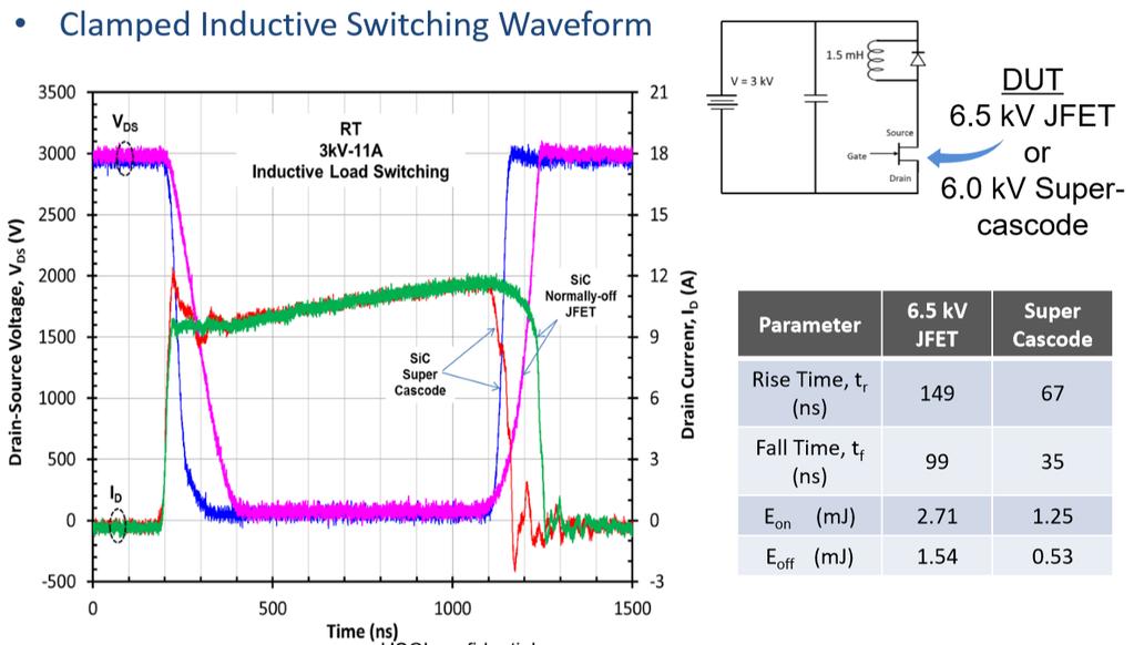
21 6.5kV SiC Module The kV Modules targets higher power (MW) applications where systems can benefit from higher DC-Link voltages and faster switching frequencies: Applications Variable Speed Industrial Motor Drives HV Battery Stacking Transformerless Grid-Tie Heavy Vehicle Traction Converters Hybridization of Ships Flywheel: High Voltage Stators Trains GVEA BESS 5kV DC-Link (Alaska)
 Sub + B/S; 0,15; 2% Epi; 5,98; 60% Source + Channel; 1,91; 19% JFET; 1,94; 19% With +15V/-5V gate drive similar to IGBTs, RdsA increases to 11.")
22 3300V MOSFETs R ds,on Breakdown (mω cm 2 ) Value Percentage Source + Channel % JFET % Epi % Sub + B/S % Total % Rds,on Breakdown (mω cm2) Sub + B/S; 0,15; 2% Epi; 5,98; 60% Source + Channel; 1,91; 19% JFET; 1,94; 19% With +15V/-5V gate drive similar to IGBTs, RdsA increases to 11.2mohmcm2 with 10us Short circuit withstand capability. 22
23 Preliminary Die Datasheet of 1700V -7.5mΩ SiC JFET


24 Technical Approach USCi prototype demonstrated
25 In development
26 Technical Approach Comparison with Other Unipolar Approaches SiC Chip Technology Half-Bridge Module Technology Approach SiC MOSFET Only SiC Stack Cascode Proposed Module Die 6.5kV MOSFET Chip 6.5kV JFET Chip 1.7kV JFET Chip R DS A 63mΩ-cm 2 63mΩ-cm 2 3mΩ-cm 2 Die Size 8.33 x 8.33 mm x 8.33 mm x 7.7 mm 2 Die Max. RT 160mΩ 160mΩ 5.5mΩ Max. RT 20mΩ 20mΩ 20mΩ Switch Configuration 8 dies in parallel 8 dies in parallel Projected Module Cost Structure (150mm epi-wafer, ~70% die yield) Module Performance 5 JFETs (each contains 2 dies in parallel) in series Total Die Count $20 / A $20 / A $11 / A Typical V 150 C 2.0V 3.7V 3.7V Practical Gate Drive -5V to + 20V Standard 0V to +12V Standard 0V to +12V Gate Charge Anti-Parallel Diode Qgs 400 nc 120 nc 30 nc Total Qg 2360 nc 400 nc 100 nc Built-in Built-in Built-in High Qrr Low Qc Low Qc Knee voltage: > 2V Knee voltage: 0.7V Knee voltage: 0.7V Due to the use of lower cost SiC 1700V devices, module cost 2X lower Much better gate charge and diode Qc

27 Ultra Low RDS,on devices Solid State Circuit Breaker 27
 Performance (Low Vf, Qrr Body-diode, switching energies) Reliability (No SiC Gate oxide, No SiC body diode, 5V Threshold voltage)")

28 Summary SiC Diodes Best-in-class performance Highest currents available USCi matched with industry leading die sizes (cost) SiC JFET Best in class devices for special applications SiC Cascodes Ease of use (12V/0V or 20V / -5V Gate Drive) Performance (Low Vf, Qrr Body-diode, switching energies) Reliability (No SiC Gate oxide, No SiC body diode, 5V Threshold voltage) Guaranteed 4us Short circuit typ 8us (highest in SiC industry) Cost (no SiC FWD necessary, lowest specific Rds,on in industry) Additional Available on: App Notes, Datasheets and SPICE models available at Various Eval Boards already available or available soon (PSFB, PFC, Flyback, LLC, H-Bridge,..) Contact: Christopher Rocneanu, Director Sales, , cro@unitedsic.com 28
29 THANK YOU! QUESTIONS? 29
Improving Totem-Pole PFC and On Board Charger performance with next generation components
 Improving Totem-Pole PFC and On Board Charger performance with next generation components Anup Bhalla 1) 1) United Silicon Carbide, Inc., 7 Deer Park Drive, Monmouth Jn., NJ USA E-mail: abhalla@unitedsic.com
Product Selector Guide. SiC FETs, SiC JFETs, and SiC Schottky Diodes
 Product Selector Guide SiC FETs, SiC JFETs, and SiC Schottky Diodes UJ3C & UF3C Series, 650/ SiC FETs Key Features Excellent body diode performance (Vf < 2V) Drive with any Si and/or SiC gate drive voltage
35mW V SiC Cascode UJ3C120040K3S Datasheet. Description. Typical Applications. Maximum Ratings
 Description United Silicon Carbide's cascode products co-package its highperformance G3 SiC JFETs with a cascode optimized MOSFET to produce the only standard gate drive SiC device in the market today.
27mW - 650V SiC Cascode UJ3C065030K3S Datasheet. Description. Typical Applications. Maximum Ratings
 Description United Silicon Carbide's cascode products co-package its highperformance G3 SiC JFETs with a cascode optimized MOSFET to produce the only standard gate drive SiC device in the market today.
80mW - 650V SiC Cascode UJ3C065080K3S Datasheet. Description. Typical Applications. Maximum Ratings
 Description United Silicon Carbide's cascode products co-package its highperformance G3 SiC JFETs with a cascode optimized MOSFET to produce the only standard gate drive SiC device in the market today.
Switch mode power supplies Low gate charge. Power factor correction modules Low intrinsic capacitance
 Description United Silicon Carbide's cascode products co-package its highperformance F3 SiC fast JFETs with a cascode optimized MOSFET to produce the only standard gate drive SiC device in the market today.
Switch mode power supplies Excellent reverse recovery. Power factor correction modules Low gate charge Motor drives Low intrinsic capacitance
 Description United Silicon Carbide's cascode products co-package its xj series highperformance SiC JFETs with a cascode optimized MOSFET to produce the only standard gate drive SiC device in the market
UF3C120080K4S. 1200V-80mW SiC Cascode DATASHEET. Description. Features. Typical applications CASE D (1) CASE G (4) KS (3) S (2) Rev.
 CASE G (4) KS (3) S (2) Rev.") 1V-8mW SiC Cascode Rev. A, January 19 DATASHEET UF3C18K4S CASE CASE D (1) Description United Silicon Carbide's cascode products co-package its highperformance F3 SiC fast JFETs with a cascode optimized
1V-8mW SiC Cascode Rev. A, January 19 DATASHEET UF3C18K4S CASE CASE D (1) Description United Silicon Carbide's cascode products co-package its highperformance F3 SiC fast JFETs with a cascode optimized
Cascode Configuration Eases Challenges of Applying SiC JFETs
 Application Note USCi_AN0004 March 2016 Cascode Configuration Eases Challenges of Applying SiC JFETs John Bendel Abstract The high switching speeds and low R DS(ON) of high-voltage SiC JFETs can significantly
Figure 1: ROHM Semiconductor SiC Diode portfolio
 SiC-Diodes, SiC-MOSFETs and Gate Driver IC The best use of SiC devices and applications are shown. Uninterruptible Power Supplies (UPS) will be described in more detail. Additional to SiC, a portfolio
Power Matters Microsemi SiC Products
 Microsemi SiC Products James Kerr Director of Marketing Power Discrete Products Microsemi Power Products MOSFETs (100V-1200V) Highest Performance SiC MOSFETs 1200V MOSFETs FREDFETs (MOSFET with fast body
10-PZ126PA080ME-M909F18Y. Maximum Ratings
 flow3xphase-sic 12V/8mΩ Features SiC-Power MOSFET s and Schottky Diodes 3 phase inverter topology with split output Improved switching behavior (reduced turn on energy and X-conduction) Ultra Low Inductance
USCi MOSFET progress (ARL HVPT program)
") USCi MOSFET progress (ARL HVPT program) L. Fursin, X. Huang, W. Simon, M. Fox, J. Hostetler, X. Li, A. Bhalla Aug 18, 2016 Contents USCi product line 1200V MOSFET progress 10kV IGBT and MPS progress 2
USCi MOSFET progress (ARL HVPT program) L. Fursin, X. Huang, W. Simon, M. Fox, J. Hostetler, X. Li, A. Bhalla Aug 18, 2016 Contents USCi product line 1200V MOSFET progress 10kV IGBT and MPS progress 2
PE6018. N-Channel Enhancement Mode Power MOSFET. Description. General Features. Application. Absolute Maximum Ratings (T C =25 unless otherwise noted)
") N-Channel Enhancement Mode Power MOSFET Description The PE6018 uses advanced trench technology and design to provide excellent R DS(ON) with low gate charge. It D can be used in a wide variety of applications.
N-Channel Enhancement Mode Power MOSFET Description The PE6018 uses advanced trench technology and design to provide excellent R DS(ON) with low gate charge. It D can be used in a wide variety of applications.
Schematic diagram R DS(ON) < V GS =10V. Marking and pin assignment Uninterruptible power supply
 < V GS =10V. Marking and pin assignment Uninterruptible power supply") FNK N-Channel Enhancement Mode Power MOSFET Description The FNK 85H21 uses advanced trench technology and design to provide excellent R DS(ON) with low gate charge. It can be used in automotive applications
FNK N-Channel Enhancement Mode Power MOSFET Description The FNK 85H21 uses advanced trench technology and design to provide excellent R DS(ON) with low gate charge. It can be used in automotive applications
GaN Based Power Conversion: Moving On! Tim McDonald APEC Key Component Technologies for Power Electronics in Electric Drive Vehicles
 1 GaN Based Power Conversion: Moving On! Key Component Technologies for Power Electronics in Electric Drive Vehicles Tim McDonald APEC 2013 2 Acknowledgements Collaborators: Tim McDonald (1), Han S. Lee
Taiwan Goodark Technology Co.,Ltd
 TGD N-Channel Enhancement Mode Power MOSFET Description The uses advanced trench technology and design to provide excellent R DS(ON) with low gate charge. It can be used in a wide variety of applications.
Device Marking Device Device Package Reel Size Tape width Quantity TO-252-2L. Parameter Symbol Limit Unit
 HM80N05K N-Channel Enhancement Mode Power MOSFET Description The uses advanced trench technology and design to provide excellent R DS(ON) with low gate charge. It can be used in a wide variety of applications.
Taiwan Goodark Technology Co.,Ltd TGD01P30
 TGD P-Channel Enhancement Mode Power MOSFET Description The uses advanced trench technology and design to provide excellent R DS(ON) with low gate charge. It can be used in a wide variety of applications.
235 W Maximum Power Dissipation (whole module) 470 T J Junction Operating Temperature -40 to 150. Torque strength
 470 T J Junction Operating Temperature -40 to 150. Torque strength") Discontinued PRODUCT SUMMARY (TYPICAL) V DS (V) 600 R DS(on) (m ) 30 GaN Power Hybrid HEMT Half-Bridge Module Features High frequency operation Free-wheeling diode not required Applications Compact DC-DC
Discontinued PRODUCT SUMMARY (TYPICAL) V DS (V) 600 R DS(on) (m ) 30 GaN Power Hybrid HEMT Half-Bridge Module Features High frequency operation Free-wheeling diode not required Applications Compact DC-DC
Parameter Symbol Limit Unit
 N-Channel Enhancement Mode Power MOSFET Description The PE3050K uses advanced trench technology and design to provide excellent R DS(ON) with low gate charge. It can be used in a wide variety of applications.
Efficiency improvement with silicon carbide based power modules
 Efficiency improvement with silicon carbide based power modules Zhang Xi*, Daniel Domes*, Roland Rupp** * Infineon Technologies AG, Max-Planck-Straße 5, 59581 Warstein, Germany ** Infineon Technologies
Taiwan Goodark Technology Co.,Ltd
 TGD N-Channel Enhancement Mode Power MOSFET Description The uses advanced trench technology and design to provide excellent R DS(ON) with low gate charge. This device is suitable for use in PWM, load switching
CREE POWER PRODUCTS 2012 REVOLUTIONIZING POWER ELECTRONICS WITH SILICON CARBIDE
 CREE POWER PRODUCTS 2012 REVOLUTIONIZING POWER ELECTRONICS WITH SILICON CARBIDE Cree, the silicon carbide expert, is leading the power semiconductor revolution. Cree, an innovator of semiconductors for
Power Semiconductors technologies trends for E-Mobility
 1 Power Semiconductors technologies trends for E-Mobility Gianni Vitale Power Conversion & Drives Section Manager System Lab, STMicroelectronics NESEM 2013, Toulouse All trademarks and logos are property
HCS65R110FE (Fast Recovery Diode Type) 650V N-Channel Super Junction MOSFET
 650V N-Channel Super Junction MOSFET") HCS65R110FE (Fast Recovery Diode Type) 650V N-Channel Super Junction MOSFET Features Very Low FOM (R DS(on) X Q g ) Extremely low switching loss Excellent stability and uniformity 100% Avalanche Tested
HCS65R110FE (Fast Recovery Diode Type) 650V N-Channel Super Junction MOSFET Features Very Low FOM (R DS(on) X Q g ) Extremely low switching loss Excellent stability and uniformity 100% Avalanche Tested
Electrical Characteristics (T A =25 unless otherwise noted) Off Characteristics Parameter Symbol Condition Min Typ Max Unit Drain-Source Breakdown Vol
 Off Characteristics Parameter Symbol Condition Min Typ Max Unit Drain-Source Breakdown Vol") N-Channel Enhancement Mode Power MOSFET Description The HM uses advanced trench technology and design to provide excellent R DS(ON) with low gate charge. It can be used in a wide variety of applications.
N-Channel Enhancement Mode Power MOSFET Description The HM uses advanced trench technology and design to provide excellent R DS(ON) with low gate charge. It can be used in a wide variety of applications.
Features. Symbol Parameter Rating Units V DS Drain-Source Voltage 60 V V GS Gate-Source Voltage ±20 V
 General Description These N-Channel enhancement mode power field effect transistors are using trench DMOS technology. This advanced technology has been especially tailored to minimize on-state resistance,
Device Marking Device Device Package Reel Size Tape width Quantity 6075K FNK6075K TO-252-2L Parameter Symbol Limit Unit
 FNK N-Channel Enhancement Mode Power MOSFET Description The FNK6075K uses advanced trench technology and design to provide excellent R DS(ON) with low gate charge. It can be used in a wide variety of applications.
High voltage GaN cascode switches shift power supply design trends. Eric Persson Executive Director, GaN Applications and Marketing
 High voltage GaN cascode switches shift power supply design trends Eric Persson Executive Director, GaN Applications and Marketing September 4, 2014 1 Outline for Today s PSMA PTR Presentation Why do we
Pitch Pack Microsemi full SiC Power Modules
 Pitch Pack Microsemi full SiC Power Modules October 2014 SiC Main Characteristics vs. Si Characteristics SiC vs. Si Results Benefits Breakdown field (MV/cm) Electron sat. velocity (cm/s) Bandgap energy
Device Marking Device Device Package Reel Size Tape width Quantity
 N-Channel Enhancement Mode Power MOSFET Description The uses advanced trench technology and design to provide excellent DS(ON) with low gate charge. It can be used in a wide variety of applications. General
VDSS (V) 650 V(TR)DSS (V) 800. RDS(on)eff (mω) max* 85. QRR (nc) typ 90. QG (nc) typ 10
 650 V(TR)DSS (V) 800. RDS(on)eff (mω) max* 85. QRR (nc) typ 90. QG (nc) typ 10") TP65H070L Series 650V GaN FET PQFN Series Preliminary Description The TP65H070L 650V, 72mΩ Gallium Nitride (GaN) FET are normally-off devices. It combines state-of-the-art high voltage GaN HEMT and low
TP65H070L Series 650V GaN FET PQFN Series Preliminary Description The TP65H070L 650V, 72mΩ Gallium Nitride (GaN) FET are normally-off devices. It combines state-of-the-art high voltage GaN HEMT and low
Device Marking Device Device Package Reel Size Tape width Quantity SIP3210 SIP3210 SOP-8 330mm
 SIAI N-Channel Enhancement Mode Power MOSFET DESCRIPTION The SIP3210 uses advanced trench technology and design to provide excellent R DS(ON) with low gate charge. It can be used in a wide variety of applications.
TO-247-3L Inner Circuit Product Summary C) RDS(on) Parameter Symbol Test Conditions Value Unit
 RDS(on) Parameter Symbol Test Conditions Value Unit") Silicon Carbide Power MOSFET N-CHANNEL ENHANCEMENT MODE TO-247-3L Inner Circuit Product Summary VDS ID(@25 C) RDS(on) 650V 110A 20mΩ Features Low On-Resistance Low Capacitance Avalanche Ruggedness Halogen
Silicon Carbide Power MOSFET N-CHANNEL ENHANCEMENT MODE TO-247-3L Inner Circuit Product Summary VDS ID(@25 C) RDS(on) 650V 110A 20mΩ Features Low On-Resistance Low Capacitance Avalanche Ruggedness Halogen
Device Marking Device Device Package Reel Size Tape width Quantity NCE85H21T NCE85H21T TO Parameter Symbol Limit Unit
 NCE N-Channel Enhancement Mode Power MOSFET DESCRIPTION The uses advanced trench technology and design to provide excellent R DS(ON) with low gate charge. It can be used in Automotive applications and
High Voltage Power MOSFET & IGBTs. Ester Spitale
 High Voltage Power MOSFET & IGBTs Ester Spitale ST HV Power MOSFETs: WW most complete offer 1500V 1000V 800V 600V 500V SuperMESH NK SuperMESH 3 K3 MDmesh II SuperMESH 5 K5 MDmesh V 200V Planar Super-junction
PWRLITE LD1010D High Performance N-Ch Vertical Power JFET Transistor with Schottky G D S
 www.lovoltech.com PWRLITE LD11D High Performance N-Ch Vertical Power JFET Transistor with Schottky Features Trench Power JFET with low threshold voltage Vth. Device fully ON with Vgs =.7V Optimum for Low
Power semiconductors technology outlook
 Power semiconductors technology outlook Francesco Di Domenico Principal Application Engineering Infineon Technologies Austria AG November 2016 Content 1 HP SMPS Application Roadmap update 2 HV power semiconductors
HCD80R600R 800V N-Channel Super Junction MOSFET
 HCD80R600R 800V N-Channel Super Junction MOSFET Features Very Low FOM (R DS(on) X Q g ) Extremely low switching loss Excellent stability and uniformity 00% Avalanche Tested Application Switch Mode Power
FNK N-Channel Enhancement Mode Power MOSFET
 FNK N-Channel Enhancement Mode Power MOSFET Description The FNK 80H11 uses advanced trench technology and design to provide excellent R DS(ON) with low gate charge. It can be used in a wide variety of
PWRLITE LU1014D High Performance N-Channel POWERJFET TM with PN Diode
 PWRLITE LU114D High Performance N-Channel POWERJFET TM with PN Diode Features Superior gate charge x Rdson product (FOM) Trench Power JFET with low threshold voltage Vth. Device fully ON with Vgs =.7V
Designing Reliable and High-Density Power Solutions with GaN
 Designing Reliable and High-Density Power Solutions with GaN 1 Detailed agenda Why is GaN Exciting GaN Fundamentals Cost and Reliability Totem Pole PFC Isolated LLC Motor Drive LiDAR Driving GaN Choosing
SUPER-SEMI SUPER-MOSFET. Super Junction Metal Oxide Semiconductor Field Effect Transistor. 800V Super Junction Power Transistor SS*80R240S
 SUPER-SEMI SUPER-MOSFET Super Junction Metal Oxide Semiconductor Field Effect Transistor 800V Super Junction Power Transistor SS*80R240S Rev. 1.1 Aug. 2017 SSP80R240S/SSF80R240S/SSB80R240S 800V N-Channel
NCE0250D. NCE N-Channel Enhancement Mode Power MOSFET. Description. General Features. Application
 http://www.ncepower.com NCE N-Channel Enhancement Mode Power MOSFET Description The uses advanced trench technology and design to provide excellent R DS(ON) with low gate charge. It can be used in a wide
Silicon Carbide N-Channel Power MOSFET
 MSC080SMA120B Datasheet Silicon Carbide N-Channel Power MOSFET Advanced Technical Information (ATI) June 2018 Contents 1 Revision History... 1 1.1 ATI... 1 2 Product Overview... 2 2.1 Features... 2 2.2
C3M K. Silicon Carbide Power MOSFET C3M TM MOSFET Technology. N-Channel Enhancement Mode. Features. Package. Benefits.
 C3M0030090K Silicon Carbide Power MOSFET C3M TM MOSFET Technology N-Channel Enhancement Mode Features Package V DS I D @ 25 C R DS(on) 900 V 63 A 30 mω C3M TM SiC MOSFET technology Optimized package with
GS66504B 650V enhancement mode GaN transistor Preliminary Datasheet
 Features 650V enhancement mode power switch Ultra low FOM Island Technology die Low inductance GaNPX package Reverse current capability Zero reverse recovery loss RoHS 6 compliant Applications On-board
VDS (V) min 600 VTDS (V) max 750 RDS(on) (mω) max* 180. Qrr (nc) typ 54. * Dynamic R(on)
 min 600 VTDS (V) max 750 RDS(on) (mω) max* 180. Qrr (nc) typ 54. * Dynamic R(on)") 600V Cascode GaN FET in TO-220 (drain tab) Description The 600V, 150mΩ gallium nitride (GaN) FET is a normally-off device. Transphorm GaN FETs offer better efficiency through lower gate charge, faster
600V Cascode GaN FET in TO-220 (drain tab) Description The 600V, 150mΩ gallium nitride (GaN) FET is a normally-off device. Transphorm GaN FETs offer better efficiency through lower gate charge, faster
100V ENHANCEMENT MODE HIGH ELECTRON MOBILITY TRANSISTOR (HEMT) Michele Rossitto. Marketing Director MOSFETs and Power ICs
 Michele Rossitto. Marketing Director MOSFETs and Power ICs") 100V ENHANCEMENT MODE HIGH ELECTRON MOBILITY TRANSISTOR (HEMT) Michele Rossitto Marketing Director MOSFETs and Power ICs 100V GaN in PowerPAK 6 x 5 mm² Package Enhancement Mode GaN Transistor Superior
100V ENHANCEMENT MODE HIGH ELECTRON MOBILITY TRANSISTOR (HEMT) Michele Rossitto Marketing Director MOSFETs and Power ICs 100V GaN in PowerPAK 6 x 5 mm² Package Enhancement Mode GaN Transistor Superior
Device Marking Device Device Package Reel Size Tape width Quantity NCE30P50G NCE30P50G DFN 5x6 EP - - -
 http://www.ncepower.com NCE P-Channel Enhancement Mode Power MOSFET Description The uses advanced trench technology and design to provide excellent R DS(ON) with low gate charge. It can be used in a wide
Device Marking Device Device Package Reel Size Tape width Quantity NCE3080K NCE3080K TO-252-2L Parameter Symbol Limit Unit
 http://www.ncepower.com NCE N-Channel Enhancement Mode Power MOSFET Description The uses advanced trench technology and design to provide excellent R DS(ON) with low gate charge. It can be used in a wide
PE2302C. N-Channel Enhancement Mode Power MOSFET 2302C DESCRIPTION GENERAL FEATURES. Application. Page 1
 N-Channel Enhancement Mode Power MOSFET DESCRIPTION The PE30C uses advanced trench technology to provide excellent R DS(ON), low gate charge and operation with gate voltages as low as.5v. This device is
Wide Band-Gap (SiC and GaN) Devices Characteristics and Applications. Richard McMahon University of Cambridge
 Devices Characteristics and Applications. Richard McMahon University of Cambridge") Wide Band-Gap (SiC and GaN) Devices Characteristics and Applications Richard McMahon University of Cambridge Wide band-gap power devices SiC : MOSFET JFET Schottky Diodes Unipolar BJT? Bipolar GaN : FET
Wide Band-Gap (SiC and GaN) Devices Characteristics and Applications Richard McMahon University of Cambridge Wide band-gap power devices SiC : MOSFET JFET Schottky Diodes Unipolar BJT? Bipolar GaN : FET
HCS80R1K4E 800V N-Channel Super Junction MOSFET
 HCS80R1K4E 800V N-Channel Super Junction MOSFET Features Very Low FOM (R DS(on) X Q g ) Extremely low switching loss Excellent stability and uniformity 100% Avalanche Tested Application Switch Mode Power
VDSS (V) 900. V(TR)DSS (V) 1000 RDS(on)eff (mω) max* 205. QRR (nc) typ 49. QG (nc) typ 10
 900. V(TR)DSS (V) 1000 RDS(on)eff (mω) max* 205. QRR (nc) typ 49. QG (nc) typ 10") 900V GaN FET in TO-220 (source tab) Description The TP90H180PS 900V, 170mΩ Gallium Nitride (GaN) FET is a normally-off device. It combines state-of-the-art high voltage GaN HEMT and low voltage silicon
900V GaN FET in TO-220 (source tab) Description The TP90H180PS 900V, 170mΩ Gallium Nitride (GaN) FET is a normally-off device. It combines state-of-the-art high voltage GaN HEMT and low voltage silicon
HCA80R250T 800V N-Channel Super Junction MOSFET
 HCA80R250T 800V N-Channel Super Junction MOSFET Features Very Low FOM (R DS(on) X Q g ) Extremely low switching loss Excellent stability and uniformity 100% Avalanche Tested Application Switch Mode Power
PRELIMINARY. VDSS (V) 600 V(TR)DSS (V) 750 RDS(on)eff (mω) max* 60. QRR (nc) typ 120. QG (nc) typ 22 PRELIMINARY
 600 V(TR)DSS (V) 750 RDS(on)eff (mω) max* 60. QRR (nc) typ 120. QG (nc) typ 22 PRELIMINARY") PRELIMINARY TPH3205ESBET 600V GaN FET in TO-268 (source tab) Description The TPH3205ESBET 600V, 49mΩ Gallium Nitride (GaN) FET is a normally-off device. It combines state-of-the-art high voltage GaN HEMT
PRELIMINARY TPH3205ESBET 600V GaN FET in TO-268 (source tab) Description The TPH3205ESBET 600V, 49mΩ Gallium Nitride (GaN) FET is a normally-off device. It combines state-of-the-art high voltage GaN HEMT
VDS (V) min 600 VTDS (V) max 750 RDS(on) (mω) max* 63. Qrr (nc) typ 136. * Dynamic R(on)
 min 600 VTDS (V) max 750 RDS(on) (mω) max* 63. Qrr (nc) typ 136. * Dynamic R(on)") 600V Cascode GaN FET in TO-247 (source tab) Not recommended for new designs see TP65H050WS Description The TPH3205WS 600V, 52mΩ gallium nitride (GaN) FET is a normally-off device. Transphorm GaN FETs offer
600V Cascode GaN FET in TO-247 (source tab) Not recommended for new designs see TP65H050WS Description The TPH3205WS 600V, 52mΩ gallium nitride (GaN) FET is a normally-off device. Transphorm GaN FETs offer
Device Marking Device Device Package Reel Size Tape width Quantity HM60N08 HM60N08 TO-220-3L - - Parameter Symbol Limit Unit
 N-Channel Enhancement Mode Power MOSFET Description The uses advanced trench technology and design to provide excellent R DS(ON) with low gate charge. It can be used in a wide variety of applications.
Taiwan Goodark Technology Co.,Ltd
 TGD N-Channel Enhancement Mode Power MOSFET Description The uses advanced trench technology and design to provide excellent R DS(ON) with low gate charge. It can be used in a wide variety of applications.
Device Marking Device Device Package Reel Size Tape width Quantity NCE82H110D NCE82H110D TO-263-2L - - -
 http://www.ncepower.com NCE N-Channel Enhancement Mode Power MOSFET Description The uses advanced trench technology and design to provide excellent R DS(ON) with low gate charge. It can be used in a wide
PJM8205DNSG Dual N Enhancement Field Effect Transistor
 DESCRIPTIONS The uses advanced trench technology to provide excellent R DS(ON), low gate charge and operation with gate voltages as low as 2.5V. This device is suitable for use as a Battery protection
Device Marking Device Device Package Reel Size Tape width Quantity NCE3090 NCE3090 TO-220-3L Parameter Symbol Limit Unit
 http://www.ncepower.com NCE N-Channel Enhancement Mode Power MOSFET Description The uses advanced trench technology and design to provide excellent R DS(ON) with low gate charge. It can be used in a wide
MP6902 Fast Turn-off Intelligent Controller
 MP6902 Fast Turn-off Intelligent Controller The Future of Analog IC Technology DESCRIPTION The MP6902 is a Low-Drop Diode Emulator IC for Flyback converters which combined with an external switch replaces
TO-220. Item Sales Type Marking Package Packaging 1 SW P 640 SW640 TO-220 TUBE 2 SW W 640 SW640 TO-3P TUBE
 N-channel MOSFET Features High ruggedness R DS(ON) (Max 0.8 Ω)@V GS =0V Gate Charge (Typical 35nC) Improved dv/dt Capability 00% Avalanche Tested 2 3 2 3. Gate 2. Drain 3. Source General Description This
Drive and Layout Requirements for Fast Switching High Voltage MOSFETs
 Drive and Layout Requirements for Fast Switching High Voltage MOSFETs Contents Introduction SuperJunction Technologies Influence of Circuit Parameters on Switching Characteristics Gate Resistance Clamp
PKP3105. P-Ch 30V Fast Switching MOSFETs
 Super Low Gate Charge % EAS Guaranteed Green Device Available Excellent CdV/dt effect decline Advanced high cell density Trench technology Product Summary BVDSS RDSON ID -3V mω -6A Description TO22 Pin
MP6901 Fast Turn-off Intelligent Controller
 MP6901 Fast Turn-off Intelligent Controller The Future of Analog IC Technology DESCRIPTION The MP6901 is a Low-Drop Diode Emulator IC that, combined with an external switch replaces Schottky diodes in
VDSS (V) 650. V(TR)DSS (V) 800 RDS(on)eff (mω) max* 180. QRR (nc) typ 52. QG (nc) typ 6.2
 650. V(TR)DSS (V) 800 RDS(on)eff (mω) max* 180. QRR (nc) typ 52. QG (nc) typ 6.2") 650V GaN FET PQFN Series Not recommended for new designs Description The TPH3206L Series 650V, 150mΩ Gallium Nitride (GaN) FETs are normally-off devices. They combine state-of-the-art high voltage GaN
650V GaN FET PQFN Series Not recommended for new designs Description The TPH3206L Series 650V, 150mΩ Gallium Nitride (GaN) FETs are normally-off devices. They combine state-of-the-art high voltage GaN
VDSS (V) 650 V(TR)DSS (V) 800 RDS(on)eff (mω) max* 180. QRR (nc) typ 47. QG (nc) typ 10
 650 V(TR)DSS (V) 800 RDS(on)eff (mω) max* 180. QRR (nc) typ 47. QG (nc) typ 10") TP65H150LSG 650V GaN FET PQFN Series Preliminary Datasheet Description The TP65H150LSG 650V, 150mΩ Gallium Nitride (GaN) FET are normally-off devices. They combine state-of-the-art high voltage GaN HEMT
TP65H150LSG 650V GaN FET PQFN Series Preliminary Datasheet Description The TP65H150LSG 650V, 150mΩ Gallium Nitride (GaN) FET are normally-off devices. They combine state-of-the-art high voltage GaN HEMT
Device Marking Device Device Package Reel Size Tape width Quantity NCE60P12K NCE60P12K TO-252-2L - - -
 http://www.ncepower.com NCE P-Channel Enhancement Mode Power MOSFET Description The uses advanced trench technology and design to provide excellent R DS(ON) with low gate charge.this device is well suited
HCS80R380R 800V N-Channel Super Junction MOSFET
 HCS8R38R 8V N-Channel Super Junction MOSFET Features Very Low FOM (R DS(on) X Q g ) Extremely low switching loss Excellent stability and uniformity % Avalanche Tested Application Switch Mode Power Supply
TPH3205WSB. 650V Cascode GaN FET in TO-247 (source tab)
") 650V Cascode GaN FET in TO-247 (source tab) Description The TPH3205WSB 650V, 52mΩ gallium nitride (GaN) FET is a normally-off device. Transphorm GaN FETs offer better efficiency through lower gate charge,
650V Cascode GaN FET in TO-247 (source tab) Description The TPH3205WSB 650V, 52mΩ gallium nitride (GaN) FET is a normally-off device. Transphorm GaN FETs offer better efficiency through lower gate charge,
Features. Description. Table 1: Device summary. Order code Marking Package Packaging SCT30N120 SCT30N120 HiP247 Tube
 Silicon carbide Power MOSFET 1200 V, 45 A, 90 mω (typ., TJ = 150 C) in an HiP247 package Datasheet - production data Figure 1: Internal schematic diagram G(1) D(2, TAB) S(3) AM01475v1_noZen Features Very
Device Marking Device Device Package Reel Size Tape width Quantity HM4884A HM4884A SOP Parameter Symbol Limit Unit
 Dual N-Channel Enhancement Mode Power MOSFET Description The HM4884A uses advanced trench technology and design to provide excellent R DS(ON) with low gate charge. It can be used in a wide variety of applications.
HCS90R1K5R 900V N-Channel Super Junction MOSFET
 HCS90RK5R 900V N-Channel Super Junction MOSFET Features Very Low FOM (R DS(on) X Q g ) Extremely low switching loss Excellent stability and uniformity 00% Avalanche Tested Application Switch Mode Power
HCS80R850R 800V N-Channel Super Junction MOSFET
 HCS80R850R 800V N-Channel Super Junction MOSFET Features Very Low FOM (R DS(on) X Q g ) Extremely low switching loss Excellent stability and uniformity 00% Avalanche Tested Application Switch Mode Power
Package. TAB Drain. Symbol Parameter Value Unit Test Conditions Note. V GS = 15 V, T C = 25 C Fig. 19 A 22 V GS = 15 V, T C = 100 C.
 C3M659J Silicon Carbide Power MOSFET C3M TM MOSFET Technology N-Channel Enhancement Mode V DS I D @ 25 C R DS(on) 9 V 35 A 65 mω Features New C3M SiC MOSFET technology New low impedance package with driver
Device Marking Device Device Package Reel Size Tape width Quantity NCE1520K NCE1520K TO-252-2L - - -
 http://www.ncepower.com NCE N-Channel Enhancement Mode Power MOSFET Description The uses advanced trench technology and design to provide excellent R DS(ON) with low gate charge. It can be used in a wide
P-Channel Enhancement Mode Power MOSFET
 DESCRIPTION The uses advanced trench technology to provide excellent R DS(ON), low gate charge and operation with gate voltages as low as 4.5V. This device is suitable for use as a load switch or in PWM
NCE6012AS. NCE N-Channel Enhancement Mode Power MOSFET. Description. General Features. Application
 http://www.ncepower.com NCE N-Channel Enhancement Mode Power MOSFET Description The uses advanced trench technology and design to provide excellent R DS(ON) with low gate charge. It can be used in a wide
Device Marking Device Device Package Reel Size Tape width Quantity NCE01P30 NCE01P30 TO-220-3L Parameter Symbol Limit Unit
 NCE P-Channel Enhancement Mode Power MOSFET Description The uses advanced trench technology and design to provide excellent R DS(ON) with low gate charge. It can be used in a wide variety of applications.
V DS =30V,I D =35A R DS(ON) < V GS =10V R DS(ON) < V GS =4.5V Schematic diagram
 < V GS =10V R DS(ON) < V GS =4.5V Schematic diagram") http://www.ncepower.com NCE N-Channel Enhancement Mode Power MOSFET Description The uses advanced trench technology and design to provide excellent R DS(ON) with low gate charge. It can be used in a wide
http://www.ncepower.com NCE N-Channel Enhancement Mode Power MOSFET Description The uses advanced trench technology and design to provide excellent R DS(ON) with low gate charge. It can be used in a wide
Prerelease Product(s) - Prerelease Product(s)
 - Prerelease Product(s)") Automotive silicon carbide Power MOSFET 650 V, 100 A, 22 mω (typ., TJ=150 C), in an HiP247 package HiP247 Figure 1: Internal schematic diagram 1 2 3 Features Datasheet - preliminary data Designed for automotive
Automotive silicon carbide Power MOSFET 650 V, 100 A, 22 mω (typ., TJ=150 C), in an HiP247 package HiP247 Figure 1: Internal schematic diagram 1 2 3 Features Datasheet - preliminary data Designed for automotive
TO-220-3L Inner Circuit Product Summary C) RDS(on) Parameter Symbol Test Conditions Value Unit
 RDS(on) Parameter Symbol Test Conditions Value Unit") H1M65B1 Silicon Carbide Power MOSFET N-CHANNEL ENHANCEMENT MODE TO-22-3L Inner Circuit Product Summary VDS ID(@25 C) RDS(on) 65V 25A 1mΩ Features Low On-Resistance Low Capacitance Avalanche Ruggedness
H1M65B1 Silicon Carbide Power MOSFET N-CHANNEL ENHANCEMENT MODE TO-22-3L Inner Circuit Product Summary VDS ID(@25 C) RDS(on) 65V 25A 1mΩ Features Low On-Resistance Low Capacitance Avalanche Ruggedness
HCD80R1K4E 800V N-Channel Super Junction MOSFET
 HCD80R1K4E 800V N-Channel Super Junction MOSFET Features Very Low FOM (R DS(on) X Q g ) Extremely low switching loss Excellent stability and uniformity 100% Avalanche Tested Application Switch Mode Power
Designing High density Power Solutions with GaN Created by: Masoud Beheshti Presented by: Xaver Arbinger
 Designing High density Power Solutions with GaN Created by: Masoud Beheshti Presented by: Xaver Arbinger Topics Why GaN? Integration for Higher System Performance Application Examples Taking GaN beyond
Turn-Off Characteristics of SiC JBS Diodes
 Application Note USCi_AN0011 August 2016 Turn-Off Characteristics of SiC JBS Diodes Larry Li Abstract SiC junction barrier schottky (JBS) diodes, as majority carrier devices, have very different turn-off
VDS (V) min 650 VTDS (V) max 800 RDS(on) (mω) max* 130. Qrr (nc) typ 54. * Dynamic R(on)
 min 650 VTDS (V) max 800 RDS(on) (mω) max* 130. Qrr (nc) typ 54. * Dynamic R(on)") 650V Cascode GaN FET in TO-220 (source tab) Description The TPH3208PS 650V, 110mΩ gallium nitride (GaN) FET is a normally-off device. Transphorm GaN FETs offer better efficiency through lower gate charge,
650V Cascode GaN FET in TO-220 (source tab) Description The TPH3208PS 650V, 110mΩ gallium nitride (GaN) FET is a normally-off device. Transphorm GaN FETs offer better efficiency through lower gate charge,
TO-220F. 1. Gate 2. Drain 3. Source. Item Sales Type Marking Package Packaging 1 SW P 4N60 SW4N60 TO-220 TUBE 2 SW F 4N60 SW4N60 TO-220F TUBE
 N-channel MOSFET Features High ruggedness R DS(ON) (Max 2.2 Ω)@V GS =0V Gate Charge (Typ 30nC) Improved dv/dt Capability 00% Avalanche Tested 2 3 TO-220F 2 3 TO-220 BS : 600V I D : 4.0A R DS(ON) : 2.2ohm
CHT-PLUTO-B1230 Preliminary Datasheet High Temperature 1200V/30A Dual SiC MOSFET Module
 The Leader in High Temperature Semiconductor Solutions CHT-PLUTO-B123 Preliminary Datasheet High Temperature 12V/3A Dual SiC MOSFET Module Version: 1.1 General description CHT-PLUTO-B123 is a high temperature
SUPER-SEMI SUPER-MOSFET. Super Junction Metal Oxide Semiconductor Field Effect Transistor. 600V Super Junction Power Transistor SS*20N60S. Rev. 1.
 SUPER-SEMI SUPER-MOSFET Super Junction Metal Oxide Semiconductor Field Effect Transistor 600V Super Junction Power Transistor SS*20N60S Rev. 1.04 September, 2013 SSW20N60S/SSA20N60S 600V N-Channel MOSFET
Features. Symbol Parameter Rating Units V DS Drain-Source Voltage 650 V V GS Gate-Source Voltage ±30 V
 General Description These N-Channel enhancement mode power field effect transistors are using Super Junction technology. This advanced technology has been especially tailored to minimize on-state resistance,
MMD50R380P 500V 0.38Ω N-channel MOSFET
 MMD50R380P 500V 0.38Ω N-channel MOSFET Description MMD50R380P is power MOSFET using magnachip s advanced super junction technology that can realize very low on-resistance and gate charge. It will provide
Ultra-Low Loss 600V 1200V GaN Power Transistors for
 Ultra-Low Loss 600V 1200V GaN Power Transistors for High Efficiency Applications David C. Sheridan, D.Y. Lee, Andrew Ritenour, Volodymyr Bondarenko, Jian Yang, and Charles Coleman, RFMD Inc., USA, david.sheridan@rfmd.com
T C =25 unless otherwise specified. Symbol Parameter Value Units V DSS Drain-Source Voltage 40 V
 40V N-Channel Trench MOSFET June 205 BS = 40 V R DS(on) typ = 3.3mΩ = 30 A FEATURES Originative New Design Superior Avalanche Rugged Technology Excellent Switching Characteristics Unrivalled Gate Charge
VDSS (V) 650 V(TR)DSS (V) 800 RDS(on)eff (mω) max* 180. QRR (nc) typ 52. QG (nc) typ 6.2 VIN=230VAC; VOUT=390VDC VIN=380VDC; VOUT=240VAC
 650 V(TR)DSS (V) 800 RDS(on)eff (mω) max* 180. QRR (nc) typ 52. QG (nc) typ 6.2 VIN=230VAC; VOUT=390VDC VIN=380VDC; VOUT=240VAC") 650V GaN FET in TO-220 (source tab) Description The TPH3206PSB 650V, 150mΩ Gallium Nitride (GaN) FET is a normally-off device. It combines state-of-the-art high voltage GaN HEMT and low voltage silicon
650V GaN FET in TO-220 (source tab) Description The TPH3206PSB 650V, 150mΩ Gallium Nitride (GaN) FET is a normally-off device. It combines state-of-the-art high voltage GaN HEMT and low voltage silicon
Device Marking Device Device Package Reel Size Tape width Quantity NCEP8818AS NCEP8818AS SOP-8 Ø330mm 12mm 2500 units
 http://www.ncepower.com NCE N-Channel Super Trench Power MOSFET Description The uses Super Trench technology that is uniquely optimized to provide the most efficient high frequency switching performance.