Transfer Function DAC architectures/examples Calibrations
|
|
|
- Gregory Osborne
- 6 years ago
- Views:
Transcription
1 Welcome to Winter semester 2012 Mixed Signal Electronic Circuits Instructor: Dr. M. Moyal Lecture 06 DIGITAL TO ANALOG CONVERTERS Transfer Function DAC architectures/examples Calibrations
2 Agenda Transfer Function DAC architectures DAC Example Calibrations
3 Transfer Function DAC Basics: D/A conversion does not change the Spectrum of the input signal Equation (Binary weighted DAC) Example A 4 bit DAC having n=4 bits will have 4 digital inputs from 0000 to (0-15) Vout (Fscale) = Vref(1/16) x [ B0 x1 + B1 x (2) + B2 x (4) + B3 x (8)]. = 15/16 x Vref Can also be called multiplying dac B s is a digital code, it is assumed a 0 value or a 1 value ( digital codes) Vref is a reference set by design to control the output range (supply range is the limitation, ~Vdd-0.6) The minimum step is assume when B0=1 all other B s are 0! Is the Least significant bit (LSB).
4 Transfer Function (TF) A n bit DAC will have the following expression n is the resolution Bo is the lsb digital control Bn-1 is the MSB digital control We set Vref, limited by process maximum range

5 Ideal TF plot Digital code Output = Digital Code x Vref (analog) Multiplication of analog value by Digital Fraction Fraction multiplication is done using Matched resistors, Current, or Capacitors
6 Misc..Frequency domain in sampling
7 Amplitude DAC output: Frequency Domain sine response no analog filter A Sinx/x Output sine wave Output reflected sine wave I A Sinx/x I 1/f noise Non linearities random noise/s ck fx Quantization noise 2fx 3fx f/2 ck-fx f
8 ISinx/xI means what! Example: If fin lies at ¼ fs! ( fs=1mhz and fin=250khz ) Pi x ¾ = 135 deg. Sin(135) / 3.14x3/4 = 0.707/2.355=0.3
 Gradient c) Random d) Single")
9 Type of mis-matches- I sources a) No error b) Gradient c) Random d) Single point
10 Thermometer unit placement architecture: Gradient affect horizontal design Horizontal gradient gradient gradient gradient gradient Common centered design Horizontal/Vertical Shufle design
11 horizontal unit placement horizontal design gradient DNL segmented Min-max=large.. INL LSB INL segmented code LSB DNL code
12 Horizontal/Vertical unit placement gradient gradient Min-max=~0.27lsb DNL INL 0.07 DNL segmented 0.05 INL segmented LSB LSB code code
13 Shuffle unit placement gradient gradient Min-max=~0.25lsb DNL INL 0.07 DNL segmented 0.15 INL segmented LSB LSB code code
14 dummies Keep background of edge unit identical Some goes to the extreem of 2 rows
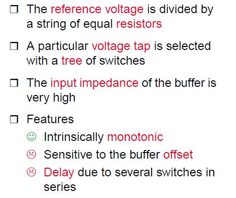
15 DACs Architectures Voltage mode: R Ladder and R-String DAC The Basic R-2R DAC R and I DAC C DAC Current (steering) DAC
16 Resistor-String DAC- basics Vmax digital code input Decoding needed analog converted outpout 12bit = 4096 resistors And 4095 switches. 12 : 4096 decoder Vmin next step in IC. remember lect1. mos as R.
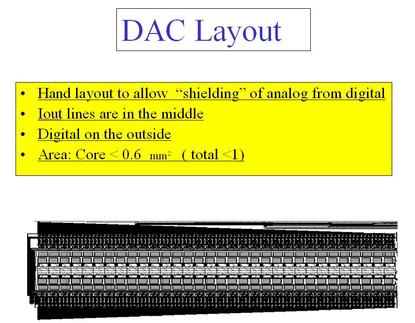
17 DAC layout / switches - Example from Pavia,
18 DAC different IDEA. 2 nd Example from Pavia,
19 Resistor DAC- basics decoder build in Digital in Analog Out 12bit = 4096 resistors And switches. No decoder! Large area..low speed.. LSB MSB
20
21 Voltage mode: R Ladder and R-String DAC Vp Vrefn Vrefp Vp R R R R R R R Vn Vout Vrefn Vrefp R R R R R R R Vn Coarse High bit Vout Vout R R R R Fine Low bit Vout
22 Voltage mode: R Ladder and R-String DAC- Equations R string - Easy to implement in CMOS, large die size (In use up 8-10b) A switch and resistor, digital selection, decoding, can be done with switch tree. Multiple R-String allow increase in resolution ( keeping monotonic) With only doubling the R string. ( Holloway 84) Need only 2N+1 resistors not 2 to the power of N. Speed is limited by amplifier input capacitance switch resistance and opamp BW Op1 op2, and op3 offset is a draw back
23 THE BASIC R-2R DAC Motivation: lower area, 12b=25 resistors No guaranteed monotonic, bad offset sensitivity
24 Vref R R R R R R R Vout a6 a5 a4 a3 a1 a0 Vmid Operation- unipolar output: msb I(a6=H)= -Vref/2R only a6 goes H I(a5=H)= -Vref/4R lsb I(a0=H)= -Vref/128R only a0=h I total = -Vref/R Vref/128R all switches to out=h Bipolar output possible with an extra amplifier and the use of Vmid
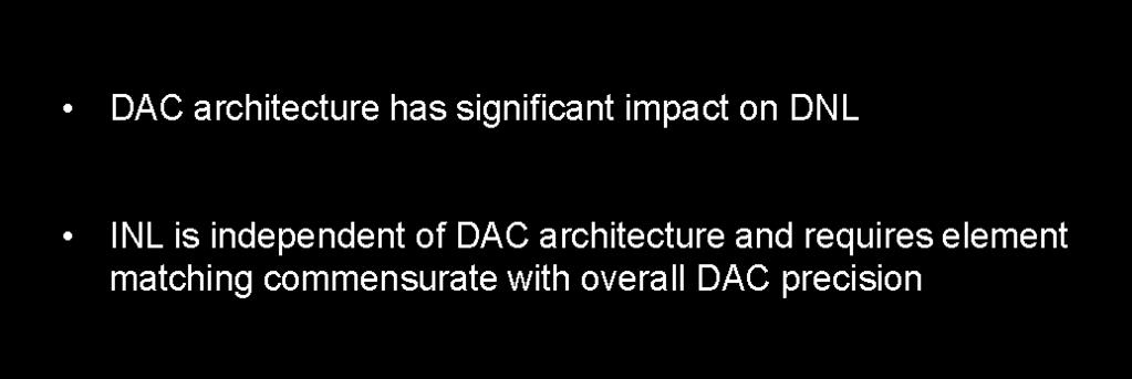
25 R-2R key issues Very common architecture if thin film resistors are used ( Cecil 74) Area efficient- Easy to increase resolution R-2R per bit Monotonic is not granted INL and DNL are closely coupled Relatively Slow rule of thumb : Matching requirement for the n th bit in the i th bit
26 1) Switch resistance, Vgs voltage changes will effect mismatches R w/l Match the switches R R w/2l 2) Problem: Output impedance changes and get multiplied by amplifier offset Looking from the other side (opamp side) R looking back form the amplifier vary with code. can we Fix the impedance issue

27 R-2R and I Source: R V Plasshe
28 Current DAC Limit: Thermal/1/f Noise of Idac, opamp (gmin), and Rf. Speed: Fast-- as opamp unity gain Band width.
29 I dac with reference

30 Glitch control Coding schemes..: Good around +/-0
31
32 DAC with..- sign magnitude..
33
34
35 C DAC 5 bit dac Ct Vdac output C1 C/2 C/4 C/8 C/16 C/32 C/32 Gnd=0v Ron Vref Gnd=0v Vdac=(C/2) / Ct(Vref) Switch every ½ cycle to 0 and re strart.. Output is valid only part of the time (switched) may need Hold switch Matching of capacitors set the INL / DNL Limit: Noise KT/C, glitches Speed: Fast-- as Ron of switch, vref settling, and and C/2 n time constant.
36 I dac - binary I dac - thermometer Could be non Monotonic- in transitions Simple decoder best for speed => Iout time constant Monotonic- guaranteed decoder complex always one change Source: B. Murmann Stanford

37 Binary Vs. Thermometer - mismatch Source : JSCC IEEE 1998 Chi-Hung 10b 500Mhz Matlab 1000 simulations FOR THE SAME AREA INL THE SAME DNL BIG DIFFERENE Figure out the optimum place: how many binary bits and how many segmented bit
38 DAC Response Inaccuracy/offset Capacitive charge Partly Source: WilleSansen 2007
39 Glitches and INL in Binary dac If the glitches scale with code (and capacitance is linear) Linearity is good
40 Combined I dac - segmented Source: B. Murmann Stanford

41 Current (steering) DAC- removed opamp Source : G. Gielen, K.U.L Leuven

42 2 option of DAC arrangements Prove DNL eq...
43
44 Current source implementation Drain Drain Drain Gate Source Source Layout Dummy one two Dummy Example_Stanford: Murmann
45 Binary Weighted Differential I/2I mode DAC TYPES Use twice the current on the bottom But only N channel switches (CML Very Fast Compact N latches ( but need to be sized up) Linearity limited by MSB DNL spikes: in some code transitions
46 Thermometer Vdd 0.5N I vb2 0.5N I r2 r1 Vmid Voutn Vout I I I I an ck latch N units N I latch a1 Current source matching relaxed (DNL) Each stage is LSB equivalent in contribution For N bit, 2 to power of N latches, unit cells, wires Silicon area is large, depend on marching and routing Power supply grounding is important I deal: Can combine with Binary approach and leave some MSB as Segmented latch a0 latch
47 DAC with reduced Rout effect and filter Fix the output impedance variations And add the «out of ban» noise reduction filter Vdd 7.5I vb2 7.5I r2 Vmid r1 Voutn Vout vb 8I 4I 2I I a3 ck msb latch latch latch a2 a1 a0 lsb latch Filter Power back-off Slow now From DAC Line Driver Virtual mid voltage Non moving
48 Pre driver
49 Dac to output path DAC[0:13] FIR interpolation filter DS current steering DAC 4th. order CT filter OUTP OUTN DAC Vdd Vnb Vpb Iout Ioutn Filter Power back-off Control From DAC Line Driver 8bit thermometer Vss Bit1 6bit binary Deglitcher & Filter to reduce out of band noise Set poles above maximum input BW
50 Calibration Methods 1) Make all I the same 2) Add error I 3) Dynamic Averaging
51 Calibration Method 1
52 Calibration Method 1
53 End lecture 06
Assoc. Prof. Dr. Burak Kelleci
 DEPARTMENT OF ELECTRICAL &ELECTRONICS ENGINEERING ANALOG-TO-DIGITAL AND DIGITAL- TO-ANALOG CONVERTERS Assoc. Prof. Dr. Burak Kelleci Fall 2018 OUTLINE Nyquist-Rate DAC Thermometer-Code Converter Hybrid
Chapter 3 Novel Digital-to-Analog Converter with Gamma Correction for On-Panel Data Driver
 Chapter 3 Novel Digital-to-Analog Converter with Gamma Correction for On-Panel Data Driver 3.1 INTRODUCTION As last chapter description, we know that there is a nonlinearity relationship between luminance
Chapter 2 Basics of Digital-to-Analog Conversion
 Chapter 2 Basics of Digital-to-Analog Conversion This chapter discusses basic concepts of modern Digital-to-Analog Converters (DACs). The basic generic DAC functionality and specifications are discussed,
Tuesday, February 22nd, 9:15 11:10. Snorre Aunet Nanoelectronics group Department of Informatics University of Oslo
 Nyquist Digital to Analog Converters Tuesday, February 22nd, 9:15 11:10 Snorre Aunet (sa@ifi.uio.no) Nanoelectronics group Department of Informatics University of Oslo February the 15th 1.1 The ideal data
Lecture 9, ANIK. Data converters 1
 Lecture 9, ANIK Data converters 1 What did we do last time? Noise and distortion Understanding the simplest circuit noise Understanding some of the sources of distortion 502 of 530 What will we do today?
Design of 8 Bit Current steering DAC
 Vineet Tiwari 1,Prof.Sanjeev Ranjan 2,Prof. Vivek Baghel 3 1 2 Department of Electronics and Telecommunication Engineering 1 2 Disha Institute of Management & Technology,Raipur,India 3 Department of Electronics
The simplest DAC can be constructed using a number of resistors with binary weighted values. X[3:0] is the 4-bit digital value to be converter to an
![The simplest DAC can be constructed using a number of resistors with binary weighted values. X[3:0] is the 4-bit digital value to be converter to an](/thumbs/73/68151962.jpg "The simplest DAC can be constructed using a number of resistors with binary weighted values. X[3:0] is the 4-bit digital value to be converter to an") 1 Although digital technology dominates modern electronic systems, the physical world remains mostly analogue in nature. The most important components that link the analogue world to digital systems are
1 Although digital technology dominates modern electronic systems, the physical world remains mostly analogue in nature. The most important components that link the analogue world to digital systems are
A Successive Approximation ADC based on a new Segmented DAC
 A Successive Approximation ADC based on a new Segmented DAC segmented current-mode DAC successive approximation ADC bi-direction segmented current-mode DAC DAC INL 0.47 LSB DNL 0.154 LSB DAC 3V 8 2MS/s
LAYOUT IMPLEMENTATION OF A 10-BIT 1.2 GS/s DIGITAL-TO-ANALOG CONVERTER IN 90nm CMOS
 LAYOUT IMPLEMENTATION OF A 10-BIT 1.2 GS/s DIGITAL-TO-ANALOG CONVERTER IN 90nm CMOS A thesis submitted in partial fulfilment of the requirements for the degree of Master of Science in Electrical Engineering
P a g e 1. Introduction
 P a g e 1 Introduction 1. Signals in digital form are more convenient than analog form for processing and control operation. 2. Real world signals originated from temperature, pressure, flow rate, force
Tuesday, March 1st, 9:15 11:00. Snorre Aunet Nanoelectronics group Department of Informatics University of Oslo.
 Nyquist Analog to Digital it Converters Tuesday, March 1st, 9:15 11:00 Snorre Aunet (sa@ifi.uio.no) Nanoelectronics group Department of Informatics University of Oslo 3.1 Introduction 3.1.1 DAC applications
DIGITALLY controlled and area-efficient calibration circuits
 246 IEEE TRANSACTIONS ON CIRCUITS AND SYSTEMS II: EXPRESS BRIEFS, VOL. 52, NO. 5, MAY 2005 A Low-Voltage 10-Bit CMOS DAC in 0.01-mm 2 Die Area Brandon Greenley, Raymond Veith, Dong-Young Chang, and Un-Ku
Data Converters. Springer FRANCO MALOBERTI. Pavia University, Italy
 Data Converters by FRANCO MALOBERTI Pavia University, Italy Springer Contents Dedicat ion Preface 1. BACKGROUND ELEMENTS 1.1 1.2 1.3 1.4 1.5 1.6 1.7 1.8 The Ideal Data Converter Sampling 1.2.1 Undersampling
CMOS ADC & DAC Principles
 CMOS ADC & DAC Principles Willy Sansen KULeuven, ESAT-MICAS Leuven, Belgium willy.sansen@esat.kuleuven.be Willy Sansen 10-05 201 Table of contents Definitions Digital-to-analog converters Resistive Capacitive
EE247 Lecture 15. EE247 Lecture 15
 EE47 Lecture 5 Administrative issues Midterm exam postponed to Tues. Oct. 8th o You can only bring one 8x paper with your own written notes (please do not photocopy) o No books, class or any other kind
Advantages of Analog Representation. Varies continuously, like the property being measured. Represents continuous values. See Figure 12.
 Analog Signals Signals that vary continuously throughout a defined range. Representative of many physical quantities, such as temperature and velocity. Usually a voltage or current level. Digital Signals
DATA CONVERSION AND LAB (17.368) Fall Class # 07. October 16, 2008
 Fall Class # 07. October 16, 2008") DATA CONVERSION AND LAB (17.368) Fall 2008 Class # 07 October 16, 2008 Dohn Bowden 1 Today s Lecture Outline Course Admin Lab #3 next week Exam in two weeks 10/30/08 Detailed Technical Discussions Digital
DATA CONVERSION AND LAB (17.368) Fall 2008 Class # 07 October 16, 2008 Dohn Bowden 1 Today s Lecture Outline Course Admin Lab #3 next week Exam in two weeks 10/30/08 Detailed Technical Discussions Digital
A 10-BIT 1.2-GS/s NYQUIST CURRENT-STEERING CMOS D/A CONVERTER USING A NOVEL 3-D DECODER
 A 10-BT 1.-GS/s NYQUST CURRENT-STEERNG CMOS D/A CONVERTER USNG A NOVEL 3-D DECODER Paymun Aliparast Nasser Nasirzadeh e-mail: peyman.aliparast@elec.tct.ac.ir e-mail: nnasirzadeh@elec.tct.ac.ir Tabriz College
EE 435. Lecture 32. DAC Design. Parasitic Capacitances. The String DAC
 EE 435 Lecture 32 DAC Design The String DAC Parasitic Capacitances . eview from last lecture. DFT Simulation from Matlab . eview from last lecture. Summary of time and amplitude quantization assessment
Digital Calibration for Current-Steering DAC Linearity Enhancement
 Digital Calibration for Current-Steering DAC Linearity Enhancement Faculty of Science and Technology, Division of Electronics & Informatics Gunma University Shaiful Nizam Mohyar, Haruo Kobayashi Gunma
Fundamentals of Data Converters. DAVID KRESS Director of Technical Marketing
 Fundamentals of Data Converters DAVID KRESS Director of Technical Marketing 9/14/2016 Analog to Electronic Signal Processing Sensor (INPUT) Amp Converter Digital Processor Actuator (OUTPUT) Amp Converter
3. DAC Architectures and CMOS Circuits
 1/30 3. DAC Architectures and CMOS Circuits Francesc Serra Graells francesc.serra.graells@uab.cat Departament de Microelectrònica i Sistemes Electrònics Universitat Autònoma de Barcelona paco.serra@imb-cnm.csic.es
Converters. 1. Introduction. 13. Converters DEEP SUBMICRON CMOS DESIGN
 13 Converters 1. Introduction Our environment is full of analog signals that we need to monitor, to capture, to treat, to store, to modify and transmit, such as sound, temperature, humidity, light, radio
Analog-to-Digital i Converters
 CSE 577 Spring 2011 Analog-to-Digital i Converters Jaehyun Lim, Kyusun Choi Department t of Computer Science and Engineering i The Pennsylvania State University ADC Glossary DNL (differential nonlinearity)
Design of Analog Integrated Systems (ECE 615) Outline
 Outline") Design of Analog Integrated Systems (ECE 615) Lecture 9 SAR and Cyclic (Algorithmic) Analog-to-Digital Converters Ayman H. Ismail Integrated Circuits Laboratory Ain Shams University Cairo, Egypt ayman.hassan@eng.asu.edu.eg
Design of Analog Integrated Systems (ECE 615) Lecture 9 SAR and Cyclic (Algorithmic) Analog-to-Digital Converters Ayman H. Ismail Integrated Circuits Laboratory Ain Shams University Cairo, Egypt ayman.hassan@eng.asu.edu.eg
Dynamic calibration of current-steering DAC
 Retrospective Theses and Dissertations Iowa State University Capstones, Theses and Dissertations 2007 Dynamic calibration of current-steering DAC Chao Su Iowa State University Follow this and additional
EE247 Lecture 14. EE247 Lecture 14
 EE47 Lecture 14 Administrative issues Midterm exam postponed to Thurs. Nov. 5th o You can only bring one 8x11 paper with your own written notes (please do not photocopy) o No books, class or any other
Hello, and welcome to the Texas Instruments Precision overview of AC specifications for Precision DACs. In this presentation we will briefly cover
 Hello, and welcome to the Texas Instruments Precision overview of AC specifications for Precision DACs. In this presentation we will briefly cover the three most important AC specifications of DACs: settling
THE pressure to reduce cost in mass market communication
 1948 IEEE JOURNAL OF SOLID-STATE CIRCUITS, VOL. 33, NO. 12, DECEMBER 1998 A 10-b, 500-MSample/s CMOS DAC in 0.6 mm Chi-Hung Lin and Klaas Bult Abstract A 10-b current steering CMOS digital-to-analog converter
Data Conversion and Lab (17.368) Fall Lecture Outline
 Fall Lecture Outline") Data Conversion and Lab (17.368) Fall 2013 Lecture Outline Class # 07 October 17, 2013 Dohn Bowden 1 Today s Lecture Outline Administrative Detailed Technical Discussions Digital to Analog Conversion Lab
Data Conversion and Lab (17.368) Fall 2013 Lecture Outline Class # 07 October 17, 2013 Dohn Bowden 1 Today s Lecture Outline Administrative Detailed Technical Discussions Digital to Analog Conversion Lab
8408 Quad 8-Bit Multiplying CMOS D/A Converter with Memory
 Quad 8-Bit Multiplying CMOS FEATURES: RAD-PAK patented shielding against natural space radiation Total dose hardness: - equal to 100 krad (Si), depending upon orbit and space mission Package: - 28 pin
+2.7V to +5.5V, Low-Power, Triple, Parallel 8-Bit DAC with Rail-to-Rail Voltage Outputs
 19-1560; Rev 1; 7/05 +2.7V to +5.5V, Low-Power, Triple, Parallel General Description The parallel-input, voltage-output, triple 8-bit digital-to-analog converter (DAC) operates from a single +2.7V to +5.5V
Area Efficient D/A Converters For Accurate DC Operation. Brandon Royce Greenley A THESIS. submitted to. Oregon State University
 Area Efficient D/A Converters For Accurate DC Operation by Brandon oyce Greenley A THESIS submitted to Oregon State University in partial fulfillment of the requirements for the degree of Master of Science
Solution to Homework 5
 Solution to Homework 5 Problem 1. a- Since (1) (2) Given B=14, =0.2%, we get So INL is the constraint on yield. To meet INL
A 130-NM CMOS 400 MHZ 8-BIT LOW POWER BINARY WEIGHTED CURRENT STEERING DAC
 A 130-NM CMOS 400 MHZ 8-BIT LOW POWER BINARY WEIGHTED CURRENT STEERING DAC Ashok Kumar Adepu and Kiran Kumar Kolupuri Department of Electronics and communication Engineering,MVGR College of Engineering,
Selecting and Using High-Precision Digital-to-Analog Converters
 Selecting and Using High-Precision Digital-to-Analog Converters Chad Steward DAC Design Section Leader Linear Technology Corporation Many applications, including precision instrumentation, industrial automation,
A 14-bit 2.5 GS/s DAC based on Multi-Clock Synchronization. Hegang Hou*, Zongmin Wang, Ying Kong, Xinmang Peng, Haitao Guan, Jinhao Wang, Yan Ren
 Joint International Mechanical, Electronic and Information Technology Conference (JIMET 2015) A 14-bit 2.5 GS/s based on Multi-Clock Synchronization Hegang Hou*, Zongmin Wang, Ying Kong, Xinmang Peng,
a Preliminary Technical Data
 a Preliminary Technical Data PELIMINAY TECHNICAL DATA FEATUES 16-bit esolution AD5543 14-btt esolution AD5553 ±1 LSB DNL ±1, ±2 or ±4 LSB INL 2mA Full Scale Current ± 20%, with V EF =10V 0.5µs Settling
Quad 12-Bit Digital-to-Analog Converter (Serial Interface)
") Quad 1-Bit Digital-to-Analog Converter (Serial Interface) FEATURES COMPLETE QUAD DAC INCLUDES INTERNAL REFERENCES AND OUTPUT AMPLIFIERS GUARANTEED SPECIFICATIONS OVER TEMPERATURE GUARANTEED MONOTONIC OVER
Quad 1-Bit Digital-to-Analog Converter (Serial Interface) FEATURES COMPLETE QUAD DAC INCLUDES INTERNAL REFERENCES AND OUTPUT AMPLIFIERS GUARANTEED SPECIFICATIONS OVER TEMPERATURE GUARANTEED MONOTONIC OVER
12 Bit 1.2 GS/s 4:1 MUXDAC
 RDA012M4 12 Bit 1.2 GS/s 4:1 MUXDAC Features 12 Bit Resolution 1.2 GS/s Sampling Rate 4:1 or 2:1 Input Multiplexer Differential Analog Output Input code format: Offset Binary Output Swing: 600 mv with
A Digitally Enhanced 1.8-V 15-b 40- Msample/s CMOS Pipelined ADC
 A Digitally Enhanced.8-V 5-b 4- Msample/s CMOS d ADC Eric Siragusa and Ian Galton University of California San Diego Now with Analog Devices San Diego California Outline Conventional PADC Example Digitally
Design of Pipeline Analog to Digital Converter
 Design of Pipeline Analog to Digital Converter Vivek Tripathi, Chandrajit Debnath, Rakesh Malik STMicroelectronics The pipeline analog-to-digital converter (ADC) architecture is the most popular topology
ELG3336: Converters Analog to Digital Converters (ADCs) Digital to Analog Converters (DACs)
 Digital to Analog Converters (DACs)") ELG3336: Converters Analog to Digital Converters (ADCs) Digital to Analog Converters (DACs) Digital Output Dout 111 110 101 100 011 010 001 000 ΔV, V LSB V ref 8 V FSR 4 V 8 ref 7 V 8 ref Analog Input
ELG3336: Converters Analog to Digital Converters (ADCs) Digital to Analog Converters (DACs) Digital Output Dout 111 110 101 100 011 010 001 000 ΔV, V LSB V ref 8 V FSR 4 V 8 ref 7 V 8 ref Analog Input
LC2 MOS Octal 8-Bit DAC AD7228A
 a FEATURES Eight 8-Bit DACs with Output Amplifiers Operates with Single +5 V, +12 V or +15 V or Dual Supplies P Compatible (95 ns WR Pulse) No User Trims Required Skinny 24-Pin DlPs, SOIC, and 28-Terminal
Summary Last Lecture
 EE247 Lecture 23 Converters Techniques to reduce flash complexity Interpolating (continued) Folding Multi-Step s Two-Step flash Pipelined s EECS 247 Lecture 23: Data Converters 26 H.K. Page 1 Summary Last
EE247 Lecture 17. EECS 247 Lecture 17: Data Converters 2006 H.K. Page 1. Summary of Last Lecture
 EE47 Lecture 7 DAC Converters (continued) DAC dynamic non-idealities DAC design considerations Self calibration techniques Current copiers Dynamic element matching DAC reconstruction filter ADC Converters
CMOS High Speed A/D Converter Architectures
 CHAPTER 3 CMOS High Speed A/D Converter Architectures 3.1 Introduction In the previous chapter, basic key functions are examined with special emphasis on the power dissipation associated with its implementation.
Calibration of current-steering D/A Converters
 Calibration of current-steering D/A Converters Citation for published version (APA): Radulov,. I., Quinn, P. J., Hegt, J. A., & Roermund, van, A. H. M. (2009). Calibration of current-steering D/A Converters.
Design of 12-bit 100-MHz Current-Steering DAC for SOC Applications
 Design of 12-bit 100-MHz Current-Steering DAC for SOC Applications Chun-Yueh Huang Tsung-Tien Hou, and Chi-Chieh Chuang Department of Electronic Engineering Kun Shan Universiv of Technology Yung-Kang,
12-Bit, Low-Power, Dual, Voltage-Output DAC with Serial Interface
 19-2124; Rev 2; 7/3 12-Bit, Low-Power, Dual, Voltage-Output General Description The dual,12-bit, low-power, buffered voltageoutput, digital-to-analog converter (DAC) is packaged in a space-saving 8-pin
The counterpart to a DAC is the ADC, which is generally a more complicated circuit. One of the most popular ADC circuit is the successive
 1 The counterpart to a DAC is the ADC, which is generally a more complicated circuit. One of the most popular ADC circuit is the successive approximation converter. 2 3 The idea of sampling is fully covered
INL PLOT REFIN DAC AMPLIFIER DAC REGISTER INPUT CONTROL LOGIC, REGISTERS AND LATCHES
 ICm ictm IC MICROSYSTEMS FEATURES 12-Bit 1.2v Low Power Single DAC With Serial Interface and Voltage Output DNL PLOT 12-Bit 1.2v Single DAC in 8 Lead TSSOP Package Ultra-Low Power Consumption Guaranteed
The need for Data Converters
 The need for Data Converters ANALOG SIGNAL (Speech, Images, Sensors, Radar, etc.) PRE-PROCESSING (Filtering and analog to digital conversion) DIGITAL PROCESSOR (Microprocessor) POST-PROCESSING (Digital
12 Bit 1.3 GS/s Master-Slave 4:1 MUXDAC. 12 BIT 4:1 MUX 1.3GS/s DAC, DIE Lead HSD Package 12 BIT 4:1 MUX 1.3GS/s DAC, 88 Lead QFP Package
 RDA012M4MS 12 Bit 1.3 GS/s Master-Slave 4:1 MUXDAC Features 12 Bit Resolution 1.3 GS/s Sampling Rate 4:1 Input Multiplexer Master-Slave Operation for Synchronous Operation of Multiple Devices Differential
DAC 10 Bits «MultiLSB»
 DAC 10 Bits «MultiLSB» Ecole de Microélectronique La Londe les Maures 12 16 Octobre 2009 on behalf IRFU s group DSM / IRFU / SEDI Constrains of the Design The KM3NET design study Underwater neutrino telescope
Summary of Last Lecture
 EE47 Lecture 7 DAC Converters (continued) Dynamic element matching DAC reconstruction filter ADC Converters Sampling Sampling switch considerations Thermal noise due to switch resistance Sampling switch
12 Bit 1.5 GS/s Return to Zero DAC
 12 Bit 1.5 GS/s Return to Zero DAC RDA112RZ Features 12 Bit Resolution 1.5 GS/s Sampling Rate 10 Bit Static Linearity LVDS Compliant Digital Inputs Power Supply: -5.2V, +3.3V Input Code Format: Offset
CENG4480 Lecture 04: Analog/Digital Conversions
 CENG4480 Lecture 04: Analog/Digital Conversions Bei Yu byu@cse.cuhk.edu.hk (Latest update: October 3, 2018) Fall 2018 1 / 31 Overview Preliminaries Comparator Digital to Analog Conversion (DAC) Analog
RESISTOR-STRING digital-to analog converters (DACs)
") IEEE TRANSACTIONS ON CIRCUITS AND SYSTEMS II: EXPRESS BRIEFS, VOL. 53, NO. 6, JUNE 2006 497 A Low-Power Inverted Ladder D/A Converter Yevgeny Perelman and Ran Ginosar Abstract Interpolating, dual resistor
IEEE TRANSACTIONS ON CIRCUITS AND SYSTEMS II: EXPRESS BRIEFS, VOL. 53, NO. 6, JUNE 2006 497 A Low-Power Inverted Ladder D/A Converter Yevgeny Perelman and Ran Ginosar Abstract Interpolating, dual resistor
10-Bit, Low-Power, Rail-to-Rail Voltage-Output Serial DAC in SOT23
 19-195; Rev 1; 1/4 1-Bit, Low-Power, Rail-to-Rail General Description The is a small footprint, low-power, 1-bit digital-to-analog converter (DAC) that operates from a single +.7V to +5.5V supply. The
OBSOLETE. 16-Bit/18-Bit, 16 F S PCM Audio DACs AD1851/AD1861
 a FEATURES 0 db SNR Fast Settling Permits 6 Oversampling V Output Optional Trim Allows Super-Linear Performance 5 V Operation 6-Pin Plastic DIP and SOIC Packages Pin-Compatible with AD856 & AD860 Audio
SPT BIT, 100 MWPS TTL D/A CONVERTER
 FEATURES 12-Bit, 100 MWPS digital-to-analog converter TTL compatibility Low power: 640 mw 1/2 LSB DNL 40 MHz multiplying bandwidth Industrial temperature range Superior performance over AD9713 Improved
Capacitance Effects ON D/A Converters
 M.Tech credit seminar report, Electronic systems group, EE. Dept. submitted in Nov.2003 Capacitance Effects ON D/A Converters Paresh Udawant (03307919) Supervisor: Prof. T. S. Rathore Abstract : This paper
A 7 bit 3.52 GHz Current Steering DAC for WiGig Applications
 A 7 bit 3.52 GHz Current Steering DAC for WiGig Applications Trindade, M. Helena Abstract This paper presents a Digital to Analog Converter (DAC) with 7 bit resolution and a sampling rate of 3.52 GHz to
Design of 10-bit current steering DAC with binary and segmented architecture
 IOSR Journal of Electrical and Electronics Engineering (IOSR-JEEE) e-issn: 2278-1676,p-ISSN: 2320-3331, Volume 13, Issue 3 Ver. III (May. June. 2018), PP 62-66 www.iosrjournals.org Design of 10-bit current
A 8-Bit Hybrid Architecture Current-Steering DAC
 A 8-Bit Hybrid Architecture Current-Steering DAC Mr. Ganesha H.S. 1, Dr. Rekha Bhandarkar 2, Ms. Vijayalatha Devadiga 3 1 Student, Electronics and communication, N.M.A.M. Institute of Technology, Karnataka,
L10: Analog Building Blocks (OpAmps,, A/D, D/A)
") L10: Analog Building Blocks (OpAmps,, A/D, D/A) Acknowledgement: Materials in this lecture are courtesy of the following sources and are used with permission. Dave Wentzloff 1 Introduction to Operational
L10: Analog Building Blocks (OpAmps,, A/D, D/A) Acknowledgement: Materials in this lecture are courtesy of the following sources and are used with permission. Dave Wentzloff 1 Introduction to Operational
System on a Chip. Prof. Dr. Michael Kraft
 System on a Chip Prof. Dr. Michael Kraft Lecture 5: Data Conversion ADC Background/Theory Examples Background Physical systems are typically analogue To apply digital signal processing, the analogue signal
Design of a Low Power Current Steering Digital to Analog Converter in CMOS
 Design of a Low Power Current Steering Digital to Analog Converter in CMOS Ranjan Kumar Mahapatro M. Tech, Dept. of ECE Centurion University of Technology & Management Paralakhemundi, India Sandipan Pine
4 Bits 250MHz Sampling Rate CMOS Pipelined Analog-to-Digital Converter
 4 Bits 250MHz Sampling Rate CMOS Pipelined Analog-to-Digital Converter Jinrong Wang B.Sc. Ningbo University Supervisor: dr.ir. Wouter A. Serdijn Submitted to The Faculty of Electrical Engineering, Mathematics
LC2 MOS 16-Bit Voltage Output DAC AD7846
 a LC2 MOS -Bit Voltage Output DAC FEATURES -Bit Monotonicity over Temperature 2 LSBs Integral Linearity Error Microprocessor Compatible with Readback Capability Unipolar or Bipolar Output Multiplying Capability
Summary Last Lecture
 EE247 Lecture 23 Converters Techniques to reduce flash complexity Interpolating (continued) Folding Multi-Step s Two-Step flash Pipelined s EECS 247 Lecture 23: Data Converters 26 H.K. Page Summary Last
EE 421L Digital Electronics Laboratory. Laboratory Exercise #9 ADC and DAC
 EE 421L Digital Electronics Laboratory Laboratory Exercise #9 ADC and DAC Department of Electrical and Computer Engineering University of Nevada, at Las Vegas Objective: The purpose of this laboratory
Current Output/Serial Input, 16-Bit DAC AD5543-EP
 Data Sheet Current Output/Serial Input, 16-Bit DAC FEATURES FUNCTIONAL BLOCK DIAGRAM 1/+2 LSB DNL ±3 LSB INL Low noise: 12 nv/ Hz Low power: IDD = 1 μa.5 μs settling time 4Q multiplying reference input
OBSOLETE. 10-Bit, 170 MSPS D/A Converter AD9731
 a FEATURES 17 MSPS Update Rate TTL/High Speed CMOS-Compatible Inputs Wideband SFDR: 66 db @ 2 MHz/ db @ 65 MHz Pin-Compatible, Lower Cost Replacement for Industry Standard AD9721 DAC Low Power: 439 mw
+2.7V to +5.5V, Low-Power, Dual, Parallel 8-Bit DAC with Rail-to-Rail Voltage Outputs
 9-565; Rev ; /99 +.7 to +5.5, Low-Power, Dual, Parallel General Description The MAX5 parallel-input, voltage-output, dual 8-bit digital-to-analog converter (DAC) operates from a single +.7 to +5.5 supply
INTEGRATED CIRCUITS. AN109 Microprocessor-compatible DACs Dec
 INTEGRATED CIRCUITS 1988 Dec DAC products are designed to convert a digital code to an analog signal. Since a common source of digital signals is the data bus of a microprocessor, DAC circuits that are
Serial Input 18-Bit Monolithic Audio DIGITAL-TO-ANALOG CONVERTER
 Serial Input 8-Bit Monolithic Audio DIGITAL-TO-ANALOG CONVERTER FEATURES 8-BIT MONOLITHIC AUDIO D/A CONVERTER LOW MAX THD + N: 92dB Without External Adjust 00% PIN COMPATIBLE WITH INDUSTRY STD 6-BIT PCM56P
An 11 Bit Sub- Ranging SAR ADC with Input Signal Range of Twice Supply Voltage
 D. Aksin, M.A. Al- Shyoukh, F. Maloberti: "An 11 Bit Sub-Ranging SAR ADC with Input Signal Range of Twice Supply Voltage"; IEEE International Symposium on Circuits and Systems, ISCAS 2007, New Orleans,
Microprocessor-Compatible 12-Bit D/A Converter AD667*
 a FEATURES Complete 12-Bit D/A Function Double-Buffered Latch On Chip Output Amplifier High Stability Buried Zener Reference Single Chip Construction Monotonicity Guaranteed Over Temperature Linearity
MEDIUM SPEED ANALOG-DIGITAL CONVERTERS
 CMOS Analog IC Design Page 10.7-1 10.7 - MEDIUM SPEED ANALOG-DIGITAL CONVERTERS INTRODUCTION Successive Approximation Algorithm: 1.) Start with the MSB bit and work toward the LSB bit. 2.) Guess the MSB
L9: Analog Building Blocks (OpAmps,, A/D, D/A)
") L9: Analog Building Blocks (OpAmps,, A/D, D/A) Acknowledgement: Dave Wentzloff Introduction to Operational Amplifiers DC Model Typically very high input resistance ~ 300KΩ v id in a v id out High DC gain
L9: Analog Building Blocks (OpAmps,, A/D, D/A) Acknowledgement: Dave Wentzloff Introduction to Operational Amplifiers DC Model Typically very high input resistance ~ 300KΩ v id in a v id out High DC gain
ELG4139: Converters Analog to Digital Converters (ADCs) Digital to Analog Converters (DACs)
 Digital to Analog Converters (DACs)") ELG4139: Converters Analog to Digital Converters (ADCs) Digital to Analog Converters (DACs) Digital Output Dout 111 110 101 100 011 010 001 000 ΔV, V LSB V ref 8 V FS 4 V 8 ref 7 V 8 ref Analog Input V
ELG4139: Converters Analog to Digital Converters (ADCs) Digital to Analog Converters (DACs) Digital Output Dout 111 110 101 100 011 010 001 000 ΔV, V LSB V ref 8 V FS 4 V 8 ref 7 V 8 ref Analog Input V
Proposing. An Interpolated Pipeline ADC
 Proposing An Interpolated Pipeline ADC Akira Matsuzawa Tokyo Institute of Technology, Japan Matsuzawa & Okada Lab. Background 38GHz long range mm-wave system Role of long range mm-wave Current Optical
Analog to Digital Conversion
 Analog to Digital Conversion Florian Erdinger Lehrstuhl für Schaltungstechnik und Simulation Technische Informatik der Uni Heidelberg VLSI Design - Mixed Mode Simulation F. Erdinger, ZITI, Uni Heidelberg
CMOS 12-Bit Multiplying DIGITAL-TO-ANALOG CONVERTER Microprocessor Compatible
 CMOS 12-Bit Multiplying DIGITAL-TO-ANALOG CONVERTER Microprocessor Compatible FEATURES FOUR-QUADRANT MULTIPLICATION LOW GAIN TC: 2ppm/ C typ MONOTONICITY GUARANTEED OVER TEMPERATURE SINGLE 5V TO 15V SUPPLY
HI Bit, 40 MSPS, High Speed D/A Converter
 October 6, 005 Pb-Free and RoHS Compliant HI7 -Bit, 40 MSPS, High Speed D/A Converter Features Throughput Rate......................... 40MHz Resolution................................ -Bit Integral Linearity
Study of R-2R DAC and Gray Code Input DAC for Glitch Reduction
 Study of R-2R DAC and Gray Code Input DAC for Glitch Reduction *Adhikari Gopal, Jian Richen, Haruo Kobayashi Kobayashi Laboratory Division of Electronics and Informatics Gunma University システム LSI 合同ゼミ
A 9.35-ENOB, 14.8 fj/conv.-step Fully- Passive Noise-Shaping SAR ADC
 A 9.35-ENOB, 14.8 fj/conv.-step Fully- Passive Noise-Shaping SAR ADC Zhijie Chen, Masaya Miyahara, Akira Matsuzawa Tokyo Institute of Technology Symposia on VLSI Technology and Circuits Outline Background
Integrated Microsystems Laboratory. Franco Maloberti
 University of Pavia Integrated Microsystems Laboratory Power Efficient Data Convertes Franco Maloberti franco.maloberti@unipv.it OUTLINE Introduction Managing the noise power budget Challenges of State-of-the-art
L9: Analog Building Blocks (OpAmps, A/D, D/A)
") L9: Analog Building Blocks (OpAmps, A/D, D/A) Courtesy of Dave Wentzloff. Used with permission. 1 Introduction to Operational Amplifiers v id in DC Model a v id LM741 Pinout out 10 to 15V Typically very
L9: Analog Building Blocks (OpAmps, A/D, D/A) Courtesy of Dave Wentzloff. Used with permission. 1 Introduction to Operational Amplifiers v id in DC Model a v id LM741 Pinout out 10 to 15V Typically very
Implementing a 5-bit Folding and Interpolating Analog to Digital Converter
 Implementing a 5-bit Folding and Interpolating Analog to Digital Converter Zachary A Pfeffer (pfefferz@colorado.edu) Department of Electrical and Computer Engineering University of Colorado, Boulder CO
Low Cost 10-Bit Monolithic D/A Converter AD561
 a FEATURES Complete Current Output Converter High Stability Buried Zener Reference Laser Trimmed to High Accuracy (1/4 LSB Max Error, AD561K, T) Trimmed Output Application Resistors for 0 V to +10 V, 5
High-Speed Analog to Digital Converters. ELCT 1003:High Speed ADCs
 High-Speed Analog to Digital Converters Ann Kotkat Barbara Georgy Mahmoud Tantawi Ayman Sakr Heidi El-Feky Nourane Gamal 1 Outline Introduction. Process of ADC. ADC Specifications. Flash ADC. Pipelined
Experiment 1: Amplifier Characterization Spring 2019
 Experiment 1: Amplifier Characterization Spring 2019 Objective: The objective of this experiment is to develop methods for characterizing key properties of operational amplifiers Note: We will be using
LC 2 MOS 16-Bit Voltage Output DAC AD7846
 Data Sheet LC 2 MOS 6-Bit Voltage Output DAC FEATURES FUNCTIONAL BLOCK DIAGRAM 6-bit monotonicity over temperature ±2 LSBs integral linearity error Microprocessor compatible with readback capability Unipolar
NON-LINEAR D/A CONVERTERS FOR DIRECT DIGITAL FREQUENCY SYNTHESIZERS ZHIHE ZHOU
 NON-LINEAR D/A CONVERTERS FOR DIRECT DIGITAL FREQUENCY SYNTHESIZERS By ZHIHE ZHOU A dissertation submitted in partial fulfillment of the requirements for the degree of DOCTOR OF PHILOSOPHY WASHINGTON STATE
IMPLEMENTING THE 10-BIT, 50MS/SEC PIPELINED ADC
 98 CHAPTER 5 IMPLEMENTING THE 0-BIT, 50MS/SEC PIPELINED ADC 99 5.0 INTRODUCTION This chapter is devoted to describe the implementation of a 0-bit, 50MS/sec pipelined ADC with different stage resolutions
Lecture 3 Switched-Capacitor Circuits Trevor Caldwell
 Advanced Analog Circuits Lecture 3 Switched-Capacitor Circuits Trevor Caldwell trevor.caldwell@analog.com Lecture Plan Date Lecture (Wednesday 2-4pm) Reference Homework 2017-01-11 1 MOD1 & MOD2 ST 2, 3,
Wideband Sampling by Decimation in Frequency
 Wideband Sampling by Decimation in Frequency Martin Snelgrove http://www.kapik.com 192 Spadina Ave. Suite 218 Toronto, Ontario, M5T2C2 Canada Copyright Kapik Integration 2011 WSG: New Architectures for