LD7790 6/11/2015. Transition-Mode PFC and Quasi-Resonant Current Mode PWM Controller. Features. General Description. Applications. Typical Application
|
|
|
- Joseph Marshall
- 6 years ago
- Views:
Transcription
1 TransiionMode PFC and QuasiResonan Curren Mode PWM Conroller REV: 05 General Descripion The feaures ransiion mode Power Facor correcion (PFC) conroller and QuasiResonan (QR) curren mode conroller for cos effecive and fewer exernal componens design of high power applicaion. The inelligen PFC swiching ON/OFF, zero curren deecion (ZCD) and frequency limiaion mechanism enable a beer efficiency under any load condiions. The device is also inegraed several funcions of proecion, such as XCAP discharge, Brownin/ou proecion, Over Load proecion (OLP), Over Temperaure Proecion (OTP), Over Volage Proecion (OVP) and Over Curren Proecion (OCP) wih High / Low Line Compensaion. Therefore i can proec he sysem from damage due o occasional failure. The is available in a SOP16 package. Feaures Inegraed PFC and QR Flyback Conroller Transiion Mode PFC Conroller QuasiResonan Operaion for Flyback Builin XCAP Discharging Brown IN/OUT Proecion Inernal SofSar Funcion Adjusmen OLP Debounce ime Exernal Lach Proecion PFC Ligh Load Turnoff Conrol OVP (Over Volage Proecion) OCP (Cycle by cycle curren limiing) 500/1200mA Driving Capabiliy Inernal OTP funcion Applicaions ACDC High Power Adaper Open Frame SMP Typical Applicaion AC Inpu EMI Filer PFCAUX PFCDRIVER PFCSENSE VOSENSE 16 HV FBDRIVER 13 7 PFC ON/OFF 6 PFCCOMP FBSENSE 10 1 FBCOMP 3 4 FBAUX GND 2 CT 14 LATCH 5 phoocoupler 1

2 Pin Configuraion SOP16 (TOP VIEW) GND FBCOMP FBAUX LATCH PFCCOMP PFCONOFF PFCAUX TOP MARK YYWWPP HV NC CT FBDRIVER PFCDRIVER PFCSENSE FBSENSE VOSENSE YY: Year code WW: Week code PP: Producion code Ordering Informaion Par number Package Top Mark Shipping GS SOP16 GS 2500 /ape & reel The is ROHS complian/ green packaged. Proecion Mode OVP Par number ( & FBAUX) OLP Exernal Lach Inernal OTP GS Auo recovery Auo recovery Lach Auo recovery 2
3 Pin Descripions Pin NAME FUNCTION 1 Supply volage pin. 2 GND Ground. 3 FBCOMP Volage feedback pin for flyback sage. Connec a phoocoupler o close he conrol loop and achieve he regulaion. 4 FBAUX Zero curren deecion and over volage proecion for flyback sage. 5 LATCH Exernal lach proecion pin. 6 PFCCOMP Oupu of he error amplifier for PFC volage loop compensaion. 7 PFCONOFF Threshold volage seing of FBCOMP for PFC ON/OFF loading conrol. 8 PFCAUX Zero curren deecion for PFC sage. 9 VOSENSE Volage sense for PFC oupu, regulaion volage is 2.5V. 10 FBSENSE Curren sense pin. Connec i o sense he Flyback MOSFET curren. 11 PFCSENSE Curren sense pin. Connec i o sense he PFC MOSFET curren. 12 PFCDRIVER Gae drive oupu o drive he exernal MOSFET for PFC. 13 FBDRIVER Gae drive oupu o drive he exernal MOSFET for Flyback. 14 CT Timer seing for Open Loop Proecion, PFC lighload urnoff and flyback sofsar. 15 NC Unconneced Pin. 16 HV Connec his pin o Line/Neural of AC main volage hrough a resisor o provide he sarup curren for he conroller. When volage increases o rip he poin of UVLO(on), his HV loop will be urned off o reduce he power loss over he sarup circui. HV pin Inernal circui will deec he AC peak volage, providing Brown in/ou and High / Low Line Deecion funcion. HV pin inernal circui will discharge Xcap s energy hrough HV curren source when AC line is disconneced. 3
4 Block Diagram HV Line Volage Deecion ACOFF Deecion HV Sarup Brownou High AC Inpu AC Off 18V / 8V 31.5V Inernal Bias 7V OVP Comparaor UVLO Comparaor OVP PDR Power Good OK GND PFCDRIVER PFCSENSE FBAUX FBCOMP PFC ON/OFF 13V 0.52V High AC Inpu: 0.40V V CT Clamp Circui & OVP Deecion V BIAS V BIAS 25.75/25µA 4.2V 2.9V Buffer Triangle Wave Generaor AC Off OK Enable PFC OVP Power Good PFC ON Proecion Curren Limi Comparaor Zero Curren Deecion Max. Freq Limi & Green Mode OLP Clock 4.5R 1R Debounce PFC ON/OFF Debounce Clock Q Heavy Load PFC ON S R PFC LEB LEB Inernal Thermal Shudown Enable PFC OVP PFC OVP Comparaor High AC Inpu PWM Comparaor S R Inernal OTP Proecion Zero Curren Q Deecor GM Enable Power Good Proecion Heavy Load High AC Inpu 4V 1.1/0.9V 2.63/2.5V V BIAS 0.65V PWM Comparaor Sofsar Comparaor Ramp Generaor V CT 8µA 2.5V 13V V BIAS 200µA PFCAUX VOSENSE PFCCOMP FBDRIVER FBSENSE CT V BIAS 1.35/1.25V Debounce Exernal Lach Auo Mode Proecion Brownou AC Off OVP/ FB OVP OLP Inernal OTP Lach Mode Proecion Exernal Lach LATCH 4
5 Absolue Maximum Raings 0.3V ~ OVP HV 0.3V ~ 500V FBCOMP, PFCCOMP, FBSENSE, PFCSENSE, FBAUX, PFCAUX, VOSENSE, LATCH, CT, PFCONOFF 0.3V ~ 6V FBDRIVER, PFCDRIVER 0.3V ~ Vcc0.3V Power Dissipaion, SOP16 600mW Package Thermal Resisance SOP16, JA 110 C/W SOP16, JC 36 C/W Juncion Temperaure 150 C Lead Temperaure (Soldering, 10sec) 260 C Sorage Temperaure Range 55 C ~ 150 C ESD Volage Proecion, Human Body Model, (Pin 3~11 and Pin 14) 3.5KV ESD Volage Proecion, Human Body Model, (Pin 1, 12, 13) 2.5KV ESD Volage Proecion, Human Body Model, (Pin 16) 1.0KV ESD Volage Proecion, Machine Model (excep HV Pin) 250V Gae Oupu Curren 500mA/1200mA Recommended Operaing Condiions Supply Volage 10V ~ 29.5V Capacior 47uF ~ 100µF HV Pin Resisor 10k ~ 50k FBCOMP Capacior Value 1nF ~ 10nF VOSENSE Capacior Value 1nF ~ 10nF PFCAUX Pin Resisor 10k ~ 30k PFCAUX Sink and Source Curren Seing 1mA Operaing Ambien Temperaure 40 C ~ 85 C Operaing Juncion Temperaure Range 40 C ~ 125 C Noe: 1. I s essenial o connec COMP pin wih a capacior o filer ou he undesired swiching noise for sable operaion. 2. Place he small signal componens closed o IC pin as possible. Cauion: Sress exceeding Maximum Raings may damage he device. Maximum Raings are sress raings only. Funcional operaion above he Recommended Operaing Condiions is no implied. Exended exposure o sress above Recommended Operaing Condiions may affec device reliabiliy. 5
6 Elecrical Characerisics (T A = 25 C unless oherwise saed, =15.0V) PARAMETER CONDITIONS SYM MIN TYP MAX UNITS HighVolage Supply (HV Pin) HighVolage Curren Source for Sarup OffSae Leakage Curren Line Volage Deecion (HV Pin) < PDR, VHV = 80V I HV ma > PDR, VHV = 80V I HV ma Afer UVLO(on), VHV = 500V I HVOFF A XCap Discharge Curren * I HVXCAP 3 ma Brownin Level V BNI V Brownou Level V BNO V Brownin BrownOu Level * V BNHYS 10 V BrownOu Debounce Time * T DBNO 75 ms High Line Trip Level V HLINE 220 V Low Line Trip Level V LLINE 184 V High Line Threshold Low Line Level Supply Volage ( Pin) Holding Curren Before UVLO (on) Operaing Curren V LINHYS 5 V < UVLO (on) I ST 150 A < UVLO (on), VLATCH = 0V VFBCOMP = 0V, PFC & Flyback OFF VFBCOMP = 3V, PFC & Flyback ON I LCH 300 A I BST 1.3 ma I 3 2 ma UVLO (off) (20 C ~125 C) V UVOFF V UVLO (on) (20 C ~125 C) V UVON V OVP Level V CCOVP V OVP Debounce Time * T DOVP 64 s Power Down Rese Volage (PDR) PFC ON/OFF Conrol (PFCONOFF pin) Source Curren for PFC OFF Threshold Seing Source Curren for PFC ON Threshold Seing PDR V I PFCOFF A I PFCON A 6
7 PARAMETER CONDITIONS SYM MIN TYP MAX UNITS PFC OFF & Open Loop Proecion Debounce Timer Seing (CT Pin) CT=0.047 F, VFBCOMP > VOLP, T DOLP 64 ms OLP Debounce Time afer sarup CT=0.047 F, VFBCOMP > VOLP, T DOLPST 74 ms a sarup * FB Sof Sar Time CT=0.047 F * T FBSS 10 ms OSCP Debounce Time CT=0.047 F, VFBCOMP > VOLP, = UVLO (off) 1V, afer sarup T DOSCP 16 ms PFC Turnoff Debounce VFBCOMP < VPFC Time ON/OFF, CT=0.047 F T DPFCOFF 1 s Exernal Lach (LATCH Pin) LATCH Pin Source Curren I LCH A TurnOn Trip Level V LATCHON V TurnOff Trip Level V LATCHOFF V OTP LATCH pin debounce ime Disable (High o Low) T DLATCHOFF s On Chip OTP (Inernal Thermal Shudown) OTP Level * T SHUTDOWN 140 C OTP Hyseresis * T RESTART 40 C PFC Oupu Volage Sensing (VOSENSE pin) Reverence Inpu Volage, V REF PFC OVP Trip Level Source Curren of VOSENSE Enable and Disable Threshold Volage VOSENSE Pull Down Resisance (20 C ~125 C) V FBREF V V PFCOVP V OVP Hyseresis V PFCOVPHYS V Debounce ime * T DPFCOVP 50 s VHV PEAK = 150V I FOLBTLV 8 A VHV PEAK = 250V I FOLBTHV 0.1 A PFC & Flyback Enable Threshold V PFCEN V PFC Disable Threshold V PFCENL V Debounce Time * T DPFCEN 50 µs R VOSENSE M 7
8 PARAMETER CONDITIONS SYM MIN TYP MAX UNITS PFC Error Amplifier (PFCCOMP Pin) Transconducance GM mho Oupu Upper Clamp Volage VOSENSE = V REF 0.1V V PCOMPMAX V Oupu Minimum Clamp Volage V PCOMPMIN V Trip Level for PFCDRIVER Sop PFC Burs Mode Trip Level for PFCDRIVER Sar PFC Maximum OnTime V PCOMPOFF V Threshold for PFCDRIVER V PCOMPON sop V 50mV PFC Max. OnTime VHV PEAK = 150V T ONMAXPLV s VHV PEAK = 250V T ONMAXPHV s PFC Minimum OffTime PFC Minimum OffTime * T POFFMIN 1 s PFC Maximum Frequency PFC Maximum Frequency F MAXPFC khz PFC Curren Sensing (PFCSENSE Pin) Curren Sense Inpu VHV PEAK = 150V V PFCCSLV V Threshold Volage VHV PEAK = 250V V PFCCSHV 0.40 V Sof Sar * FBSENSE = 0.05~0.52V T PFCSS 10 ms Leading Edge Blanking ime T LEBPFC ns PFC Zero Curren Deecor (PFCAUX Pin) Upper Clamp Volage IPFCAUX = 3mA V PFCAUXUC V PFC ZCD Trip Level V PFCAUXH V Delay from PFCAUX o Oupu * T DPFCZCD 200 ns PFC ZCD Time Ou Afer PFCDRIVER Turnoff T TOPFC s 8
9 PARAMETER CONDITIONS SYM MIN TYP MAX UNITS Flyback Comp Pin (FBCOMP Pin) Shor Circui Curren V COMP=0V I FBCOMPSC ma Flyback Burs Mode Trip Level for FBDRIVER Sar V BSTONQR V Trip Level for FBDRIVER Sop V BSTOFFQR V Heavy Load Trigger Level V IFBCSEN V Open Loop Volage FBCOMP pin open V FBC V Over Load Proecion (FBCOMP Pin) OLP Trigger Level (VOLP) V OLP V Oupu Shor Circui Proecion OSCP Trigger Level * VFBCOMP > VOLP V CCOSCP UVLO (off) 2 V Flyback OVP (FBAUX pin) OVP Trigger Curren I FBAUXOVP A Upper Clamp Volage IFBAUX = 0.3mA V FBAUXH V Debounce Cycle * T DFBAUXOVP 4 FB PWM cycle FBAUX OVP Deecion Blanking Time * Afer FBDRIVER Turnoff T DFBOVPDET 2 s Zero Curren Deecion (FBAUX Pin) Lower Clamp Volage IFBAUX = 1mA V FBAUXLC V Flyback ZCD Trip Level V QRDLQR 50 mv Flyback ZCD Delay Time * T DFBZCD 200 ns Flyback ZCD Time Ou1 Afer Max. Frequency T O1QR s Minimum Flyback ZCD Time Ou2 Afer FBDRIVER Turnoff T O2QR s ZCD Blanking Time Afer FBDRIVER Turnoff T OFFMINQR s Oscillaor for Swiching Frequency Flyback Max. Frequency F MAXQR khz Flyback Max. Frequency Mode Threshold, V FBCOMP * V FBCFMAX 2.2 V Flyback Green Mode Frequency F GREENQR khz Flyback Green Mode Threshold, V FBCOMP * V FBCGREEN 1.0 V Flyback Maximum On Time T ONMAXQR s 9
10 PARAMETER CONDITIONS SYM MIN TYP MAX UNITS Flyback Curren Sensing (FBSENSE Pin) Threshold for Cycle by Cycle Curren Limi, Vcs(off) (20 C ~125 C) V OCQR V Leading Edge Blanking Time T LEBQR ns OCP Compensaion Curren VHV PEAK = 250Vdc FBCOMP = 3V I FBCSHV A Delay o Oupu * T DCS 80 ns PFC and Flyback Gae Drive Oupu (PFCDRIVER & FBDRIVER Pin) Oupu Low Level =15V, I SINK=100mA V OUTH V Oupu High Level =15V, I SOURCE =100mA V OUTL 9.0 V Oupu High Level =9V, I SOURCE =2mA V OUTH2 8.5 V Oupu High Clamp Level =17V V OUTCL 13 V Rising Time * =15V, CL=2700pF T OUTR 130 ns Falling Time * =15V, CL=2700pF T OUTF 45 ns Noes: Guaraneed by design. 10
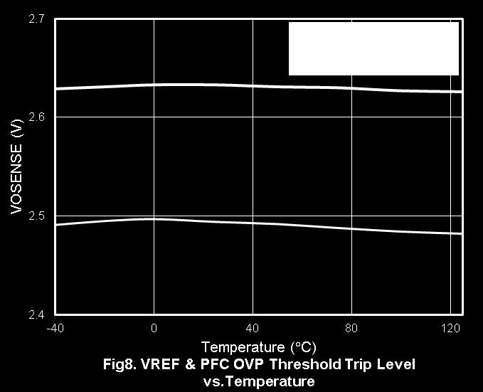
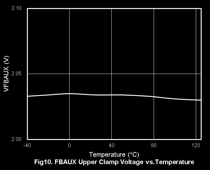
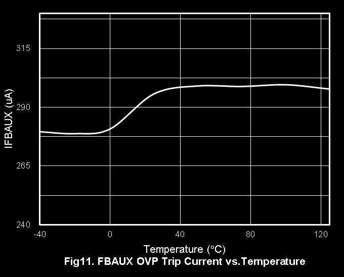
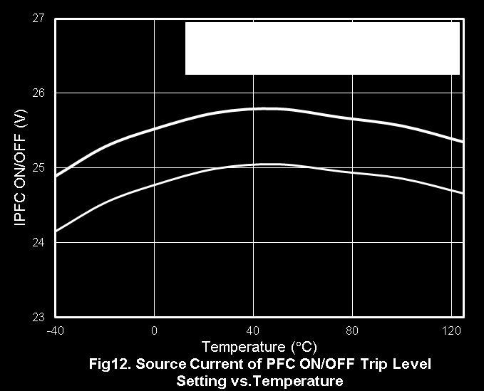
11 Typical Performance Characerisics 11


12 Typical Performance Characerisics 12
13 Typical Performance Characerisics 13
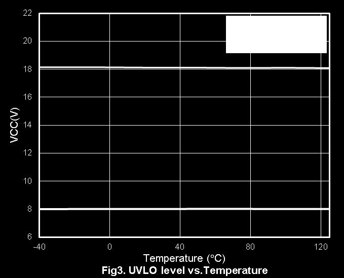
14 Applicaion Informaion Operaion Overview As long as he green power requiremen becomes a rend and he power saving is geing more and more imporan for he swiching power supplies and swiching adapors, he radiional PWM conrollers are no able o suppor such new requiremens. Furhermore, he cos and size limiaion force he PWM conrollers need o be powerful o inegrae more funcions o reduce he exernal par couns. The is ideal for hese applicaions o provide an easy and cos effecive soluion; is deailed feaures are described as below. Inernal HighVolage Sarup Circui and Under Volage Lockou (UVLO) The radiional circui provides he sarup curren hrough a sarup resisor o power up he PWM conroller. However, i consumes oo much power o mee he curren power saving requiremen. In mos cases, sarup resisors carry larger resisance and ake more ime o sar up. As shown in Fig 15, THE is implemened wih a highvolage sarup circui o minimize power loss on sarup circui. During he sarup phase, a highvolage curren source sinks curren from AC Line or Neural o provide he sarup curren and charge he capacior C1 a he same ime. Refer o Fig 16. If is below PDR, he charge curren is only 1.5mA and he lower charge curren can proec IC if he Pin is shored o GND. Once volage rises up o reach he UVLO(on) hreshold, HV pin will no longer charge he capacior and insead, send a gae drive signal o draw supply curren for from he auxiliary winding of he ransformer. Tha minimizes he power loss on he sarup circui successfully. An UVLO comparaor is embedded o deec he volage across pin o ensure he supply volage is high enough o power on he and in addiion o drive he power MOSFET. As shown in Fig 16, a hyseresis is provided o preven THE from shudown by he volage dip during sarup. The urnon and urnoff hreshold level are se a 18V and 8V respecively. For beer EMI performance, i s recommend o connec HV pin o he inpu erminals of bridge diode, as Fig 15. AC inpu UVLO(on) UVLO(off) PDR HV curren source PWM IC Vcc GND HV Curren 1.5mA Holding Curren (~150uA) 3mA Vcc curren FBSENSE Fig 15. ~ ~ Operaion &Swiching ~ 0mA (off) Rs C1 D1 Operaing Curren (Supply from Auxiliary Winding) Fig
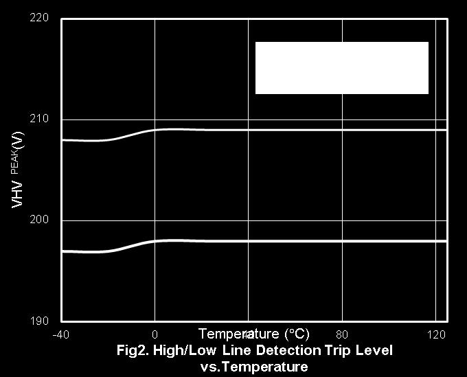
15 Oupu Driver Sage The device builds a CMOS buffer respecively in he sages of PFC and Flyback, wih ypical 500mA/1200mA driving capabiliy, o drive he power MOSFET direcly. The oupu volage is clamped a 13V o proec he MOSFET gae even when he volage is over 13V. Brown In/ Ou Proecion The feaures Brownin / Brownou proecion on HV pin. As he builin comparaor deecs line volage, i will urn off he conroller o preven from any damage. In case VHV < Brownou Level, he oupu driver will be disabled even when already reaches UVLO (on). I herefore forces hiccup beween ULVO (on) and UVLO (off). Unless he line volage is large enough and over Brownin Level, he oupu driver will no sar swiching even if he nex ULVO (on) is ripped. A hyseresis is designed o preven from falseriggering and damage o he exernal componens during urnon and urnoff phase. See Fig 17 for he operaion. Line Volage High Line and Low Line Deecion The HV pin can deeced AC inpu level o conrol source curren of VOSENSE Pin and OCP compensaion logic. During AC inpu variaions, he source curren of VOSENSE and OCP compensaion logic show as below. VHV PEAK High Line Trip Level Low Line Trip Level Source Curren of VOSENSE OCP Comp. Logic > 220V 0A Enable < 184V 8µA Disable Line Volage VHV(peak) Low Line area High Line area Low Line area I VOSENSE 8µA 0A OCP Compensaion VHV(peak) BNO/on Disable Enable Disable BNO/off Fig 18. Vcc XCap Discharge Funcion UVLO(on) UVLO(off) The EMI filer has a paralleled discharging resisor across Xcapacior. To mee safey requiremen, his componen FBDRIVER is required o be discharged in less han 1sec, ha is, Discharge CX Cap RDischarg e 1sec NonSwiching Fig 17. Swiching Non Swiching The power loss of his resisor is in direc proporion o square of inpu volage. For example, if he inpu volage is 264Vac and he discharging resisance ~ 2M, 35mW, we can conclude he power loss by follow equaion. 15
16 2 VAC (RMS) PLoss RDischarge To eliminae he significan power loss from his discharging resisor, applies he innovaive paen echnology o discharge Xcap s energy hrough HV curren source when AC line is disconneced. Fig 19 shows he operaion. By applying his echnology, he sysem can easily pass he safey es wihou discharging resisor and reduce power loss. If i s unplugged, he AC volage across Xcap will sill remain he same. The deecs HV pin o monior he AC volage across Xcap. If AC volage across Xcap rises or falls beyond he limi of he hreshold, he HV scheme will sink consan curren o GND o discharge i in around 75ms of debounce ime under any load condiion. decreased, FBCOMP volage becomes lower and he swich frequency can be reduced under he ligh load condiion. This feaure helps o enhance he efficiency in ligh load condiions. The curve shows as Fig 20. To mee he requiremen of European 'EMCdirecive', i s necessary o adop a soluion wih PFC conrol. In order o enhance efficiency a ligh load, he feaures PFC conrol and is able o shu down swiching o reduce power consumpion. As FBCOPM volage falls below PFC ON/OFF volage hreshold, he PFC conroller will sop PFCDRIVER swiching unil FBCOMP volage resume o is level. See Fig 21 for he block. 85kHz 30kHz AC inpu ~ ~ Cbulk FBCOMP 0.6V 1V 2.2V Fig 20. Max. Frequency Limi of Flyback V BIAS C1 D1 FBCOMP V BIAS 2.9V AC deeced CKT Gae CS PFC ON/OFF 25.75/25µA V BIAS PFC ON/OFF Debounce PFC ON Clock for PFC OFF debounce PWM IC Rs GND Fig 19. Flyback Green Mode and PFC Turnoff Conrol THE uses maximum frequency limi scheme o conrol flyback swiching frequency, and i depends on he level of FBCOMP volage. When oupu loading is CT V CT Fig 21. PFC Oupu Volage Seing moniors he oupu volage signal from VOSENSE pin hrough a resisor divider pair of RA and 16
17 RB. A ransconducance amplifier is used for i o replace he convenional volage amplifier. The oupu curren of he amplifier changes according o he volage difference of he invering and noninvering inpu of he amplifier. The oupu volage of he amplifier is compared wih he inernal ramp signal o generae he urnoff signal. A curren is flowed ou of he VOSENSE Pin (8µA) during low line condiion. The PFC oupu volage is deermined by he following relaionship. PFC Over Volage Proecion To preven unsable volage occurred o he PFC oupu capacior under faul condiion, he is implemened wih OverVolage Proecion on VOSENSE pin. If VOSENSE volage rises over he OVP hreshold of 2.63V, he oupu driver circui will be shu down simulaneously o sop he swiching of he power MOSFET unil VOSENSE volage drops o 2.5V. Fig 23 shows is operaion. High Line: PFC V O = 2.5V (1 RA RB//R VOSENSE ) (1) 2.63V 2.50V VOSENSE OVP Tripped Low Line: PFC V O RA ( RB//R = (2.5V 8μA RB//R VOSENSE VOSENSE ) 2.5V (2) Where RA and RB are values for op and boom feedback resisor (as shown in he Fig 22). Once he value of PFC V O is deermined, hen subsiue he value of RA/RB obained from he formula (1) o (2) o ge he RB value. ) PFCDRIVER Swiching Non Swiching Fig 23. OVP Clear Swiching Non Swiching AC Line Inpu PFC Zero Curren Deecion PFC Vo Fig 24 shows PFC Zero Curren Deecion (ZCD) block. As he auxiliary winding coupled wih he inducor deecs HV PFC OVP PFC OVP Comparaor 2.63/2.5V RA he curren over he boos inducor drops o zero, he ZCD block will swich on he exernal MOSFET. This feaure allows ransiionmode operaion. If he volage of he Line Volage Deecion PWM Comparaor High Line GM V BIAS 8µA 2.5V R VOSENSE VOSENSE PFCCOMP RB PFCAUX pin rises above 0.2V, he ZCD comparaor will urn on he MOSFET. The PFCAUX pin is proeced inernally by 4Vhigh clamp and 0Vlow clamp. The 50µs imer will generae a MOSFET urnon signal if he oupu driver has been a low level for over 50µs. Ramp Generaor Fig
18 PFCDRIVER RZ VAUX RAMP COMP PFCAUX Resar Timer ID I PEAK Inducor Curren zero 0A T on T dis 4V 0.1/0.2V S R Q PFCDRIVER PFCSENSE RCS n aux/n p V IN AUX Volage I NEG 0V Fig 24. Delay Time 4V n aux/n p (V OUT V IN) Fig 25 shows ypical ZCDrelaed waveforms. Rz will produce some delay because of he parasiic capaciance on PFCAUX pin. Before he swich urns on wih he delay, PFCAUX Volage V OUT 0.2V he sored charge of he C OSS (MOSFET oupu capacior) will be discharged o a small filer capacior C IN1 wih a bridge diode hrough he pah indicaed in Fig 26. So he V DS Minimum Volage Turnon 0V inpu curren I IN1 drains o zero a he ime. Here, i s recommended o se source curren of PFCAUX pin around 1mA. Rz could be obained from he below formula and is also adjusable o conrol he urnon iming of he swich. MAX NAUX,PFC RZ PFC Vo 1mA NP,PFC AC I IN C IN1 Fig 25. L D V OUT I L Q C OSS C o Fig 26. PFC Curren Sensing The deecs he PFC MOSFET curren across PFCSENSE pin o proec he MOSFET, which is for he cyclebycycle curren limi. The maximum volage hreshold of PFCSENSE pin is se a 0.52V. The MOSFET peak curren can be obained as below. 0.52V IPEAK(MAX) RPFCS A 250ns leadingedge blanking (LEB) ime is buil in PFCSENSE pin o preven he falserigger from he curren spike. The RC filer is eliminable in some low power applicaions, such as he pulse widh of he urnon 18
19 spike below 250ns and he negaive spike on PFCSENSE pin is below 0.3V. However, he pulse widh of he urnon spike is deermined according o he oupu power, circui design and PCB layou. I is srongly recommended o adop a smaller RC filer for high power applicaion o avoid PFCSENSE pin being damaged by he negaive urnon spike. PFCDRIVER PFCSENSE GND R PFCS RC filer is required when he negaive spike exceeds 0.3V or he oal spike widh is over 250nS LEB period. Fig 27. Flyback Volage Feedback Loop The volage feedback signal is provided from he TL431 on he secondary side hrough he phoocoupler o FBCOMP pin of he and fed o he volage divider wih 1/5.5 raio. Tha is, V V FBCOMP FBSENSE(PWM ) COMPARATOR 5.5 A pullhigh resisor is embedded inernally o opimize he exernal circui. Flyback Curren Sensing & OCP Compensaion Design Tip The feaures curren mode of flyback conrol. I receives boh curren signal and volage signal o form he conrol loop and achieve regulaion. deecs he primary MOSFET curren across FBSENSE pin for peak curren mode and also limis he curren cyclebycycle. The maximum volage hreshold of FBSENSE pin is se a 0.65V. Thus he MOSFET peak curren can be calculaed as: I PEAK(MAX) 0.65V R FBS In general, he power converer provides various curren signals o reflec he inpu volage wih propagaion delay ime. To compensae i, an offse volage is added o he FBSENSE signal by an inernal curren source (200µA) and an exernal resisor (R OCP) beween he sense resisor (R FBS) and FBSENSE pin, as shown in Fig 28. The compensaion curren is only enabled when FBCOMP volage is above 2.9V a high line condiion. ROCP: 220~1k ; COPC: 47p~470pF. As PFC behaves in curren sensing, a 350nS leadingedge blanking (LEB) ime is incorporaed in he inpu of FBSENSE pin o preven falseriggering from he curren spike. FBCOMP > 2.9V High AC Inpu VBIAS 200µA FBDRIVER FBSENSE R OCP Flyback Burs Mode Conrol Curren Limi Comparaor 0.65V C OCP R FBS The oupu driver of he can be disabled immediaely by pulling FBCOMP pin volage level below FBDRIVER Sop Trip Level. The disablemode can be released when FBCOMP pin volage level is pulled high above FBDRIVER sar rip level. Proecion Mode Fig 28. There are wo kinds of proecion modes available in he. 19
20 AuoRecovery Proecion Mode As AuoRecovery proecion circui laches he operaion, he gae oupu will swich for a shor erm as every ime rises back o UVLO(ON). I herefore forces he hiccup beween UVLO(ON) and UVLO(OFF). As soon as he faul condiion is removed, he sysem will resume i operaion righ away. Fig 29 shows he operaion. UVLO(on) UVLO(off) AC Inpu UVLO(on) UVLO(off) PDR Lach Mode Proecion Signal è Remove he Abnormal Condiion AuoRecovery Proecion Signal è Remove he Abnormal Condiion Gae Driver Swiching Swiching Gae Driver Swiching Swiching Swiching Fig 29. Lach Proecion Mode As Lach ype proecion circui laches he operaion, he gae oupu will remain in off sae even when he reaches UVLO(ON). The sysem is unable o recover unless i is repowered o le drop below Power Down Rese (PDR) and hen ramps over UVLO(on). Fig 30 shows he operaion. Fig 30. Over Load Proecion (OLP) Auo Recovery To proec he circui from being damaged a overload condiion, shor or open loop condiion, he is implemened wih smar OLP funcion. The feaures auo recovery funcion. See Fig 31 for he waveform. In such faul condiion, he feedback sysem will force he volage loop o ener sauraion and hen pull high he volage over FBCOMP pin (VFBCOMP). When VFBCOMP ramps up o he OLP ripped level (4.2V) for longer han he OLP delay ime, he proecion will be acivaed o urn off he oupu driver and o sop he swiching of power circui. The OLP delay ime is se by CT pin. I is o preven he false riggering during he ransien condiion of poweron and urnoff. A divide4 couner is implemened o reduce he average power under OLP behavior. Whenever OLP is acivaed, he oupu is lached off and he divide4 couner sars o coun he number of UVLO(off). The proecion mode will 20
21 no be released and he oupu will no be resumed unil he 4h UVLO(off) level is ripped. Wih he proecion mechanism, he average inpu power will be reduced, so ha he componen emperaure and sress can be conrolled wihin he safe operaing area. UVLO(on) UVLO(off) COMP OLP 4nd UVLO(off) Proecion Rese oupu driver righ away and disable he power MOSFET unil he UVLO(on) is ripped. The OVP funcion is auorecoverable. If he OVP condiion, usually caused by openloop of feedback, is no released, he will rip he OVP level again and reshudown he oupu driver. This makes work in hiccup mode. Fig 32 shows is operaion. Afer he OVP condiion is removed, will keep in is normal operaion level and he oupu driver also reurn o he normal operaion. OLP Delay Time OVP Level OVP Tripped VOLP OUT OLP rip Level UVLO(on) UVLO(off) FBDRIVER / PFCDRIVER OUT Clamping Swiching NonSwiching Swiching NonSwiching Swiching Fig 31. Swiching Fig 32. Oupu Shor Circui Proecion (OSCP) If he oupu of he sysem is shorcircuied, Vo and will drop immediaely. Due o he operaing of he volage loop, FBCOMP volage will be pulled high a he same ime. If he siuaion coninues o pull FBCOMP high over 4.2V for over 16ms and drops below 10V, i will acivae OSCP proecion agains damage and urn off he gae driver. OVP on Auo Recovery The maximum raing of he is abou 32.5V. To proec he in overvolage condiion, i is implemened wih OVP funcion on. Once volage rises over he OVP hreshold, i will urn off he Flyback Zero Curren Deecion Fig 33 shows flyback Zero Curren Deecion (ZCD) block. As PFC behaves in ZCD, as soon as he auxiliary winding coupled wih he inducor deecs he curren over he flyback ransformer drops o zero, he ZCD block will swich on he exernal MOSFET. This feaure enables QuasiResonan operaion. The FBAUX uses falling edge o rigger ZCD o urn on FBDRIVER and he rigger level is 0.05V as shown in Fig 34. FBAUX pin is builin wih 2Vhigh clamp and 0Vlow clamp. 21
22 R ZCD V AUX FBAUX FBDRIVER ZCD Signal 0.05/0.15 2V Time Ou Managemen Freq. Limi & Timing Conrol Managemen Fig 33. Turnon delay FBDRIVER Turnon ransformed ino a curren signal. The sinking curren of FBAUX is, N I AUX FBAUX = [(VO VD ) NS 2V] / RZCD The samples he signal afer FBDRIVER urnoff wih 2µs delay o perform oupu over volage proecion. This 2µs delay ime is used o ignore he volage ringing from leakage inducance of PWM ransformer. The sampled curren level is compared wih inernal hreshold curren 300µA. If he sampled curren exceeds he OVP rip level, an inernal couner will sar o coun he subsequen OVP evens. The couner has been added o preven incorrec OVP deecion which migh occur during ESD or lighning evens. If 4 flyback PWM cycles of he subsequen OVP evens are deeced, he OVP circui will swich he power MOSFET off. Vo VD NS: NAUX RZCD VAUX FBAUX 2V 300µA FBOVP Debounce 0.05V AUX Winding Sampling LEB Conrol Fig 35. FBDRIVER Max Frequency Limi Fig 34. OVP on FBAUX Auo Recovery FBAUX also provide over volage proecion(ovp). An oupu overvolage proecion is implemened in he, as shown in Fig 35 and Fig 36. I senses he auxiliary winding volage by he resisor, R ZCD. The auxiliary winding volage is refleced on he secondary winding and herefore he fla volage on FBAUX pin is in proporion o he oupu volage. The fla volage can be AUX Winding 2µs Sampling Signal Fig 36. N (Vo VD ) N AUX S 22
23 OnChip OTP Auo Recovery An inernal OTP circui is embedded in he o provide he worscase proecion. When he chip VLATCH 1.35V 1.25V OTP Exernal Lach Release emperaure rises over he rip OTP level, he oupu driver will be disabled unil he chip is cooled down below he hyseresis emperaure. UVLO(on) UVLO(off) PDR Exernal Lach The Exernal Lach funcion is implemened o sense wheher here is any hospo of power circui like power MOSFET or oupu recifier. Once an overemperaure condiion is deeced, he OTP will be acivaed o shu down he. Typically, an NTC is recommended o connec o LATCH pin. The NTC resisance will decrease as he device or ambien says in high emperaure. The relaionship is shown below. VLATCH 80μA R NTC When V LATCH < Turnoff Trip (yp. 1.25V), i will rigger he proecion o shu down he oupu driver and lach off he power supply. The will remain lached unless he drops below PDR (power down rese) and rise over UVLO(on). I requires wo condiions o resar he successfully. Cool down he circui so ha he NTC resisance will increase and raise V LATCH above 1.35V. Then replug in AC power. The deailed operaion is show in Fig 37. AC inpu Volage FBDRIVER, PFCDRIVER Swiching AC Off Lach Mode Released NonSwiching Fig 37. Adjusable Timer on CT Pin AC On (Recycle) Swiching Connec CT pin wih an exernal capaciance o generae clock for imer. The OLP debounce, PFC Turnoff debounce and flyback Sofsar period are se according he below able. C CT FB Sofsar period OLP Debounce Time PFC Turnoff Debounce 22nF 4.6ms 30ms 0.47s 47nF 10.0ms 64ms 1.00s 68nF 14.0ms 93ms 1.45s 100nF 21.2ms 136ms 2.13s 23
24 PullLow Resisor on he Gae Pin of MOSFET The consiss of an anifloaing resisor a PFCDRIVER and FBDRIVER pin o preven he oupu driver in any abnormal condiion which may false rigger MOSFET. Even so, we sill recommend adding an exernal one a he MOSFET gae erminal o provide more proecion in case of disconnecion of gae resisor R G during poweron. In such singlefaul condiion, as shown in Fig 38, he resisor R8 can provide a discharge pah o avoid he MOSFET from being falseriggered by he curren hrough he gaeodrain capacior C GD. Therefore, he gae of MOSFET should be always pulled low and kep in he offsae as he gae resisor is disconneced or opened in any case. V IN Leadrend s proprieary of HiV echnology will eliminae parasiic SCR in THE. Fig 40 shows he equivalen HiV srucure circui of THE. THE is more capable o susain negaive volage han similar producs. However, a 10K resisor is recommended o be added in he HiV pah o play as a curren limi resisor whenever a negaive volage is applied. Negaiveriggered Parasiic SCR. Small negaive spike on HV pin will cause he lachup beween Vcc and GND. 0V HV Fig 39. GND Oher HV process wih parasiic SCR PFCDRIVER FBDRIVER dvin i = Cgd d C GD 0V Curren limi resisor for Prevening damage from Negaive volage (recommended) Rg HV R8 GND CS Parasiic effec beween HV, Vcc and GND GND This resisor would proec he MOSFET from being false riggered by he curren hrough C GD, if R G is disconneced. Fig 38. Proecion Resisor on he HV Pah In some oher HiV process and design, here may be a parasiic SCR formed beween HV pin, and GND. As shown in Fig 39, a small negaive spike on he HV pin may rigger his parasiic SCR and cause lachup beween and GND. I may damage he chip because of he equivalen shorcircui induced by such lachup behavior. Fig 40. PCB Layou Guideline The consiss of a pair of gae drivers. Here are some guide lines o layou he PCB o suppress he noise caused from he effecs beween PFC and flyback. The PCB layou diagram is shown as Fig Separae small signal curren loop from gae driver or curren loop. 2. Separae curren loop from PFC gae driver o minimize he effec from flyback ZCD. 24
25 3. Minimize he race lengh beween GND pin and he curren sense resisor. 4. Be aware o roue he HV pin AWAY from he oher races for i possesses high volage. Flyback RCS PFC RCS High Curren Loop (Gae Driver, ) Low Curren Loop (Small Signal) Fig 41. GND FBCOMP FBAUX LATCH PFCCOMP VINSENSE PFCAUX Inrush Curren of PFC HV HVS CT FBDRIVER PFCDRIVER PFCSENSE FBSENSE VOSENSE High Volage Trace During fas AC powers on/off, inrush curren will flow hrough PFC choke if bulk capacior volage is lower han AC line volage. Once PFC conroller remains operaion in such condiion, large curren will flow in PFC MOSFET during gae urnon phase, shown as 錯誤! 找不到參照來 源. So, i's necessary o selec a MOSFET of proper curren sress o avoid damage Under his condiion, during MOSFET gae urnon and urnoff period, some MOSFET will couple wih he high frequency energy, generaed from parasiic elemen as inrush curren resonaes ino he conroller. See Fig 43 for i. The gae driver of conroller could be damaged by he exernal energy. Add a bead core in he gae driver curren loop o blank he high frequency energy from damage, shown as Fig 44. And place an exra bypass diode here o limi inrush curren of PFC choke helps o minimize he risk, shown as Fig 45. I PFCDRIVER Fig 43. Fig 44. IL ID VIN _ VDS _ PFC VO _ VGS _ I L Cycle by cycle curren limi Fig 45. Zoom in I L I D Cycle by cycle curren limi V GS Minimum onime Fig

26 Package Informaion SOP16 Symbols Dimensions in Millimeers Dimensions in Inch MIN MAX MIN MAX A B C D F 1.27 TYP TYP. H I J M θ Imporan Noice Leadrend Technology Corp. reserves he righ o make changes or correcions o is producs a any ime wihou noice. Cusomers should verify he daashees are curren and complee before placing order. 26
27 Revision Hisory REV. Dae Change Noice 00 9/11/2013 Original Specificaion. 01 1/27/2014 Typical Applicaion add PFC wih inrush curren bypass diode Fixed UNITs, 1. From NF o nf 2. From Ns o ns 3. Flyback Burs Mode, Trip Level for FBDRIVER Sop: from mv o V Add Recommended Operaing Condiion: 1. VOSENSE Capacior Value 2. PFCAUX Pin Resisor 3. PFCAUX Sink and Source Curren Add iems for Applicaion Informaion 1. Add VOSENSE Pull Down Resisor Informaion 2. Add Inrsush Curren of PFC 02 7/30/2014 Correc rule of dae code. 03 4/16/2015 Spec JC is added. The max power dissipaion and juncion emperaure are changed. 04 4/30/2015 Spec iems are changed: 1. The ypical value of FBSS is changed. 2. Parameers DOVP, DPFCOVP, DPFCEN and DFBAUXOVP, DCS are guaraneed by design. 3. The CCT Pin imer able is modified. 4. Pin configuraion figure is correced. 05 Parameers I HVXCAP, V BNHYS, T DOLPST and T FBSS are guaraneed by design. 27
LD7830H 06/27/2012. High Power Factor Flyback LED Controller with HV Start-up. Features. General Description. Applications. Typical Application
 06/27/2012 High Power Facor Flyback LED Conroller wih HV Sar-up Rev: 00 General Descripion The LD7830H is a HV sar-up Flyback PFC conroller, specially designed for LED lighing appliances. I operaes in
LD7539H 12/24/2012. Green-Mode PWM Controller with BNO and OTP Protections. General Description. Features. Applications. Typical Application. Rev.
 12/24/2012 Green-Mode PWM Conroller wih BNO and OTP Proecions Rev. 00 General Descripion The LD7539H is buil-in wih several funcions, proecion and EMI-improved soluion in a iny package. I akes less componens
LD /07/2015. Green-Mode PWM Controller with Variable Frequency and Brown IN/OUT Protections. Features. General Description.
 GreenMode PWM Conroller wih Variable Frequency and Brown IN/ Proecions REV. 01 General Descripion The is buil wih several funcions, proecion and EMIimproved soluion in a iny package. I akes less componen
LD7516C 08/31/2016. Primary Side Quasi-Resonant Controller. Features. General Description. Applications. Typical Application REV.
 REV. 01 General Descripion Primary ide Quasi-Resonan Conroller The is an excellen primary side feedback MO conroller wih CV/CC operaion, inegraed wih several funcions of proecions. I minimizes he componen
LD5761B 04/27/2015. High Voltage with Two-Level Frequency. Green-Mode PWM Controller. General Description. Features. Applications. Typical Application
 REV: 00 General Descripion High Volage wih Two-Level Frequency The is a Green Mode PWM IC which is buil-in wih brown-in/ou funcions in a SOP-7/SOP-8 package. The device could minimize he componen couns,
LD5760A 12/15/2016. High Voltage Green-Mode PWM Controller with BNO Function. Features. General Description. Applications. Typical Application REV.
 High Volage Green-Mode PWM Conroller wih BNO Funcion REV. 06 General Descripion The is a Green Mode PWM IC buil-in wih brown-in/ ou funcions in a SOP-7 or SOP-8 package. I minimizes he componen couns,
LD7515L 8/5/2015. Primary Side Quasi-Resonant BJT Controller with CV/CC Operation. Features. General Description. Applications. Typical Application
 Primary ide Quasi-esonan BJT Conroller wih CV/CC Operaion EV. 00 General Descripion The is an excellen primary side feedback BJT conroller wih CV/CC operaion, inegraed wih several funcions of proecions.
Primary Side Control SMPS with Integrated MOSFET
 General Descripion GG64 is a primary side conrol SMPS wih an inegraed MOSFET. I feaures programmable cable drop compensaion and a peak curren compensaion funcion, PFM echnology, and a CV/CC conrol loop
GG6005. General Description. Features. Applications DIP-8A Primary Side Control SMPS with Integrated MOSFET
 General Descripion GG65 is a primary side conrol PSR SMPS wih an inegraed MOSFET. I feaures a programmable cable drop compensaion funcion, PFM echnology, and a CV/CC conrol loop wih high reliabiliy and
AOZ7111. Critical Conduction Mode PFC Controller. Features. General Description. Applications. Typical Application AOZ7111
 Criical Conducion Mode PFC Conroller General Descripion The AOZ7111 is an acive power facor correcion (PFC) conroller for boos PFC applicaions ha operae in criical conducion mode (CRM). The device uses
CURRENT MODE PWM+PFM CONTROLLER WITH BUILT-IN HIGH VOLTAGE MOSFET
 CURRENT MODE PWM+PFM CONTROLLER WITH BUILT-IN HIGH VOLTAGE MOSFET DESCRIPTION SD6835 is curren mode PWM+PFM conroller used for SMPS wih buil-in high-volage MOSFET and exernal sense resisor. I feaures low
ORDER INFORMATION TO pin 320 ~ 340mV AMC7150DLF
 www.addmek.com DESCRIPTI is a PWM power ED driver IC. The driving curren from few milliamps up o 1.5A. I allows high brighness power ED operaing a high efficiency from 4Vdc o 40Vdc. Up o 200KHz exernal
LD /14/2013. Green-Mode PWM Controller with HV Start-Up Circuit and Soft Start time Adjustment. Features. General Description.
 06/14/2013 Green-Mode PWM Controller with HV Start-Up Circuit and Soft Start time Adjustment REV. 01 General Description The brings high performance, highly integrated functions, protections and EMI-improve
LD7752B 6/11/2013. Green-Mode PWM Controller with HV Start-Up Circuit and Soft Start time Adjustment. Features. General Description.
 6/11/2013 Green-Mode PWM Controller with HV Start-Up Circuit and Soft Start time Adjustment REV. 00 General Description The brings high performance, highly integrated functions, protections and EMI-improve
Version 2.1, 6 May 2011
 Version 2.1, 6 May 2011 Off-Line SMPS Curren Mode Conroller wih inegraed 650V CoolMOS and Sarup cell (frequency jier Mode) in FullPak Power Managemen & Supply N e v e r s o p h i n k i n g. Revision Hisory:
Synchronization of single-channel stepper motor drivers reduces noise and interference
 hronizaion of single-channel sepper moor drivers reduces noise and inerference n mos applicaions, a non-synchronized operaion causes no problems. However, in some cases he swiching of he wo channels inerfere,
Ultracompact 6-Channel Backlight and Flash/Torch White LED Driver
 Feaures and Benefis Proprieary adapive conrol scheme (1, 1.5, 2 ) 0.5% ypical LED curren maching 2 separae serial inerfaces for dimming conrol Drives up o 6 whie LEDs (4 display backligh, 2 flash/orch)
LD7536R 05/11/2010. Green-Mode PWM Controller with Frequency Swapping and Integrated Protections. General Description. Features.
 05/11/2010 Green-Mode PWM Controller with Frequency Swapping and Integrated Protections Rev. 00 General Description The LD7536R is built-in with several functions, protection and EMI-improved solution
LD7830 VSEN GND ISEN COMP
 8/17/2012 High Power Factor Flyback LED Controller with HV Start-up REV: 01a General Description The LD7830 is a HV start-up Flyback PFC controller, specially designed for LED lighting appliances. It operates
Fixed-Frequency, 800V CoolSET in DS0-12 Package
 ICE3AR1080JG Fixed-Frequency, 800V CoolSET in DS0-12 Package Produc Highlighs 800 V avalanche rugged CoolMOS wih sarup cell Acive Burs Mode o reach he lowes Sandby Power
Fixed-Frequency, 650V CoolSET in DS0-12 Package
 ICE3RBR4765JG Fixed-Frequency, 650V CoolSET in DS0-12 Package Produc Highlighs Acive Burs Mode o reach he lowes Sandby Power
Design of Power Factor Correction Circuit Using AP1662
 Applicaion Noe 075 Design of Power Facor Correcion Circui Using AP66 Prepared by Wang Zhao Kun ysem Engineering Deparmen. nroducion. Produc Feaures The AP66 is an acive power facor conrol C which is designed
Application Note 5324
 Desauraion Faul Deecion Opocoupler Gae Drive Producs wih Feaure: PLJ, PL0J, PLJ, PL1J and HCPLJ Applicaion Noe 1. Inroducion A desauraion faul deecion circui provides proecion for power semiconducor swiches
LD7838GR. High Power Factor Flyback LED Controller. with HV Start-up. Features. General Description. Applications. Typical Application 11/22/2016
 High Power Factor Flyback LED Controller with HV Start-up REV. 01 General Description The is a 700V HV start-up active PFC Flyback controller, specially designed for LED lighting application. This device
LD7577 1/15/2009. High Voltage Green-Mode PWM Controller with Brown-Out Protection. General Description. Features. Applications. Typical Application
 Rev. 01 General Description High Voltage Green-Mode PWM Controller with Brown-Out Protection The LD7577 integrates several functions of protections, and EMI-improved solution in SOP-8 package. It minimizes
LD7536E 5/28/2012. Green-Mode PWM Controller with Frequency Swapping and Integrated Protections. General Description. Features.
 5/28/2012 Green-Mode PWM Controller with Frequency Swapping and Integrated Protections Rev. 00 General Description The is built-in with several functions, protection and EMI-improved solution in a tiny
LD /15/2011. Green-Mode PWM Controller with Frequency Swapping and Integrated Protections. Features. General Description.
 12/15/2011 Green-Mode PWM Controller with Frequency Swapping and Integrated Protections Rev. 02a General Description The LD7536 is built-in with several functions, protection and EMI-improved solution
CoolSET -F3R ICE3BR4765JG. Off-Line SMPS Current Mode Controller with integrated 650V CoolMOS and Startup cell (frequency jitter Mode) in DSO-16
 in DSO-16") Version 2.0, 18 Feb 2010 CoolSET -F3R Off-Line SMPS Curren Mode Conroller wih inegraed 650V CoolMOS and Sarup cell (frequency jier Mode) in DSO-16 Power Managemen Supply Never sop hinking. Revision Hisory:
Version 2.0, 18 Feb 2010 CoolSET -F3R Off-Line SMPS Curren Mode Conroller wih inegraed 650V CoolMOS and Sarup cell (frequency jier Mode) in DSO-16 Power Managemen Supply Never sop hinking. Revision Hisory:
LD /01/2013. Boost Controller for LED Backlight. General Description. Features. Applications. Typical Application REV: 00
 04/01/2013 Boost Controller for LED Backlight REV: 00 General Description The LD5861 is a wide-input asynchronous current mode boost controller, capable to operate in the range between 9V and 28V and to
Control circuit for a Self-Oscillating Power Supply (SOPS) TDA8385
 TDA8385") FEATURES Bandgap reference generaor Slow-sar circuiry Low-loss peak curren sensing Over-volage proecion Hyseresis conrolled sand-by funcion Error amplifier wih gain seing Programmable ransfer characer
FEATURES Bandgap reference generaor Slow-sar circuiry Low-loss peak curren sensing Over-volage proecion Hyseresis conrolled sand-by funcion Error amplifier wih gain seing Programmable ransfer characer
CoolSET -F3R ICE3RBR4765JZ. Off-Line SMPS Current Mode Controller with integrated 650V CoolMOS and Startup cell (frequency jitter Mode) in DIP-7
 in DIP-7") Version 2.0, 7 Jun 2013 CoolSET -F3R ICE3RBR4765JZ Off-Line SMPS Curren Mode Conroller wih inegraed 650V CoolMOS and Sarup cell (frequency jier Mode) in DIP-7 Power Managemen Supply Never sop hinking.
Version 2.0, 7 Jun 2013 CoolSET -F3R ICE3RBR4765JZ Off-Line SMPS Curren Mode Conroller wih inegraed 650V CoolMOS and Sarup cell (frequency jier Mode) in DIP-7 Power Managemen Supply Never sop hinking.
N e v e r s t o p t h i n k i n g.
 Version 2.1, 30 Aug 2011 N e v e r s o p h i n k i n g. Revision Hisory: 2011-8-30 Daashee Previous Version: V2.0 Page Subjecs (major changes since las revision) 27 revised ouline dimension for PG-DIP-7
F3 PWM controller ICE3AS03LJG. Off-Line SMPS Current Mode Controller with integrated 500V Startup Cell ( Latched and frequency jitter Mode )
") Version 2.0, 3 Jul 2009 F3 PWM conroller Off-Line SMPS Curren Conroller wih inegraed 500V Sarup Cell ( Lached and frequency jier ) Power Managemen Supply Never sop hinking. F3 PWM conroller Revision Hisory:
Version 2.0, 3 Jul 2009 F3 PWM conroller Off-Line SMPS Curren Conroller wih inegraed 500V Sarup Cell ( Lached and frequency jier ) Power Managemen Supply Never sop hinking. F3 PWM conroller Revision Hisory:
CoolSET -F3R ICE3BR4765J. Off-Line SMPS Current Mode Controller with integrated 650V CoolMOS and Startup cell (frequency jitter Mode) in DIP-8
 in DIP-8") Version 2.5, 19 Nov 2012 CoolSET -F3R Off-Line SMPS Curren Mode Conroller wih inegraed 650V CoolMOS and Sarup cell (frequency jier Mode) in DIP-8 Power Managemen Supply Never sop hinking. Revision Hisory:
Version 2.5, 19 Nov 2012 CoolSET -F3R Off-Line SMPS Curren Mode Conroller wih inegraed 650V CoolMOS and Sarup cell (frequency jier Mode) in DIP-8 Power Managemen Supply Never sop hinking. Revision Hisory:
CoolSET -F3 ICE3A1065ELJ. Off-Line SMPS Current Mode Controller with integrated 650V CoolMOS and Startup Cell (Latched and frequency jitter Mode)
") Version 2.3, 19 Nov 2012 CoolSET -F3 Off-Line SMPS Curren Conroller wih inegraed 650V CoolMOS and Sarup Cell (Lached and frequency jier ) Power Managemen & Supply Never sop hinking. Revision Hisory: 2012-11-19
Version 2.3, 19 Nov 2012 CoolSET -F3 Off-Line SMPS Curren Conroller wih inegraed 650V CoolMOS and Sarup Cell (Lached and frequency jier ) Power Managemen & Supply Never sop hinking. Revision Hisory: 2012-11-19
CoolSET -F3R ICE3BR1765J. Off-Line SMPS Current Mode Controller with integrated 650V CoolMOS and Startup cell (frequency jitter Mode) in DIP-8
 in DIP-8") Version 2.3, 19 Nov 2012 CoolSET -F3R Off-Line SMPS Curren Mode Conroller wih inegraed 650V CoolMOS and Sarup cell (frequency jier Mode) in DIP-8 Power Managemen & Supply Never sop hinking. Revision Hisory:
Version 2.3, 19 Nov 2012 CoolSET -F3R Off-Line SMPS Curren Mode Conroller wih inegraed 650V CoolMOS and Sarup cell (frequency jier Mode) in DIP-8 Power Managemen & Supply Never sop hinking. Revision Hisory:
LED System Driver IC ICLS8023Z. Data Sheet. Industrial & Multimarket
 LED Sysem Driver IC Off-Line LED Curren Mode Conrollers wih Inegraed 800 V CoolMOS & Sarup Cell Daa Shee Version 1.0, 2011-09-26 Indusrial & Mulimarke Ediion 2011-09-26 Published by Infineon Technologies
PROFET BTS 736 L2. Smart High-Side Power Switch Two Channels: 2 x 40mΩ Status Feedback
 PROFET BTS 736 2 Smar igh-side Power Swich Two Channels: 2 x 40mΩ Saus Feedback Produc Summary Package Operaing olage bb(on) 4.75...41 Acive channels one wo parallel On-sae Resisance R ON 40mΩ 20mΩ Nominal
Discontinued Product
 Disconinued Produc This device is no longer in producion. The device should no be purchased for new design applicaions. Samples are no longer available. Dae of saus change: November 1, 2010 Recommended
Excellent Integrated System Limited
 Excellen Inegraed Sysem Limied Socking Disribuor Click o view price, real ime Invenory, Delivery Lifecycle Informaion: Infineon Technologies For any quesions, you can email us direcly: sales@inegraed-circui.com
CoolSET -F3R80 ICE3AR4780CJZ. Off-Line SMPS Current Mode Controller with integrated 800V CoolMOS and Startup cell (brownout & CCM) in DIP-7
 in DIP-7") Version 2.0, 19 Apr 2013 CoolSET -F3R80 Off-Line SMPS Curren Mode Conroller wih inegraed 800V CoolMOS and Sarup cell (brownou & CCM) in DIP-7 Power Managemen & Supply Never sop hinking. Revision Hisory:
Version 2.0, 19 Apr 2013 CoolSET -F3R80 Off-Line SMPS Curren Mode Conroller wih inegraed 800V CoolMOS and Sarup cell (brownou & CCM) in DIP-7 Power Managemen & Supply Never sop hinking. Revision Hisory:
Step Down Voltage Regulator with Reset TLE 6365
 Sep Down Volage Regulaor wih Rese TLE 6365 Feaures Sep down converer Supply Over- and Under-Volage-Lockou Low Oupu volage olerance Oupu Overvolage Lockou Oupu Under-Volage-Rese wih delay Overemperaure
LD5857 4/15/2014. Boost Controller for LED Backlight. General Description. Features. Applications. Typical Application REV: 00
 4/15/2014 Boost Controller for LED Backlight REV: 00 General Description The LD5857 is a wide-input asynchronous current mode boost controller, capable to operate in the range between 9V and 28V and to
LD7523 6/16/2009. Smart Green-Mode PWM Controller with Multiple Protections. General Description. Features. Applications. Typical Application REV: 00
 6/16/2009 Smart Green-Mode PWM Controller with Multiple Protections REV: 00 General Description The LD7523 is a low startup current, current mode PWM controller with green-mode power-saving operation.
Programmable DC Electronic Loads 8600 Series
 Daa Shee Programmable DC Elecronic Loads The programmable DC elecronic loads provide he performance of modular sysem DC elecronic loads in a compac benchop form facor. Wih fas ransien operaion speeds and
Smart High-Side Power Switch Two Channels: 2 x 30mΩ Current Sense
 POFET Smar High-Side Power Swich Two Channels: 2 x 3mΩ Curren Sense Produc Summary Package Operaing olage (on) 5...34 Acive channels one wo parallel On-sae esisance ON 3mΩ 15mΩ Nominal load curren (NOM)
HI-8585, HI ARINC 429 Line Driver PIN CONFIGURATION DESCRIPTION SUPPLY VOLTAGES FUNCTION TABLE FEATURES PIN DESCRIPTION TABLE
 February DESCRIPTION The HI-8585 and HI-858 are CMOS inegraed circuis designed o direcly drive he ARINC 49 bus in an 8-pin package. Two logic inpus conrol a differenial volage beween he oupu pins producing
Programmable DC Electronic Load 8600 Series
 Daa Shee Programmable DC Elecronic Load The programmable DC elecronic loads provide he performance of modular sysem DC elecronic loads in a compac benchop form facor. Wih fas ransien operaion speeds and
Programmable DC Electronic Loads 8600 Series
 Daa Shee Programmable DC Elecronic Loads 99 Washingon Sree Melrose, MA 02176 Phone 781-665-1400 Toll Free 1-800-517-8431 Visi us a www.tesequipmendepo.com 2U half-rack 3U 6U USB RS232 GPIB The programmable
Application Note AN-1083
 Applicaion Noe AN-1083 Feaures of he Low-Side Family IPS10xx By Fabio Necco, Inernaional Recifier Table of Conens Page Inroducion...1 Diagnosis...1 Inpu Curren vs. Temperaure...1 Selecion of he Resisor
CoolSET F3R80 ICE3AR0680VJZ
 Off-Line SMPS Curren Mode Conroller wih inegraed 800V CoolMOS and Sarup cell (inpu OVP & frequenc y jier) in DIP -7 Daa Shee V2.1 2013-10-22 Power Managemen & Mulimarke Ediion 2013-10-22 Published by Infineon
TEA2019 CURRENT MODE SWITCHING POWER SUPPLY CONTROL CIRCUIT DIRECT DRIVE OF THE EXTERNAL SWITCHING TRANSISTOR POSITIVE AND NEGATIVE OUTPUT CUR-
 CURRENT MODE SWITCHING POWER SUPPLY CONTROL CIRCUIT DIRECT DRIVE OF THE EXTERNAL SWITCHING TRANSISTOR POSITIVE AND NEGATIVE OUTPUT CUR- RENTS UP TO 05A CURRENT LIMITATION TRANSFORMER DEMAGNETIZATION AND
Package. Applications
 Primary-side Regulaion PWM Conroller for Auomoive Applicaions SFA2 Daa Shee Descripion The SFA2 is he swiching power supply IC for flyback circui and has high accuracy error amplifier. When he load of
VIPer12ADIP / VIPer12AS
 VIPer2ADIP / VIPer2AS OFF LINE BATTERY CHARGER ADAPTER TARGET SPECIFICATION TYPE R DS(on) I N V DSS VIPer2ADIP VIPer2AS 30Ω 0.36A 730V n FIXED 50 khz SWITCHING FREQUENCY n 8V TO 40V WIDE RANGE VOLTAGE
Quasi-Resonant Controller
 ICE5QSAG Quasi-Resonan Conroller Produc Highlighs Novel Quasi-resonan operaion and proprieary implemenaion for low EMI Enhanced Acive Burs Mode wih selecable enry and exi sandby power Acive Burs Mode o
 Disribued by: www.jameco.com 1-800-831-4242 The conen and copyrighs of he aached maerial are he propery of is owner. 16K-Bi CMOS PARALLEL E 2 PROM FEATURES Fas Read Access Times: 200 ns Low Power CMOS
SCiCoreDrive62 +DC T5 U V W -DC. SCiCore 62. IGBT/MOSFET drivers
 PRELIMINARY TECHNICAL INFORMATION SCiCoreDrive62 IGBT/MOSFET drivers HIGHLIGHTS - 6 channel IGBT driver - suiable for 200V IGBT (900 V max on DCLink) - Up o 8 A peak oupu curren - Collecor sensing & faul
PI90LV9637. LVDS High-Speed Differential Line Receivers. Features. Description. Applications PI90LV9637
 LVDS High-Speed Differenial Line Receivers Feaures Signaling Raes >400Mbps (200 MHz) Single 3.3V Power Supply Design Acceps ±350mV (ypical) Differenial Swing Maximum Differenial Skew of 0.35ns Maximum
MX6895BETR. -550V Full Bridge Gate Driver INTEGRATED CIRCUITS DIVISION. Features. Description. Applications. Ordering Information
 -550V Full Bridge Gae Driver INTEGRATED CIRCUITS DIVISION Feaures Full Bridge Gae Driver Inernal High Volage Level Shif Funcion Negaive 550V Lamp Supply Volage 3V o 12V CMOS Logic Compaible 8V o 12V Inpu
P. Bruschi: Project guidelines PSM Project guidelines.
 Projec guidelines. 1. Rules for he execuion of he projecs Projecs are opional. Their aim is o improve he sudens knowledge of he basic full-cusom design flow. The final score of he exam is no affeced by
PRM and VTM Parallel Array Operation
 APPLICATION NOTE AN:002 M and V Parallel Array Operaion Joe Aguilar VI Chip Applicaions Engineering Conens Page Inroducion 1 High-Level Guidelines 1 Sizing he Resisor 4 Arrays of Six or More Ms 5 Sysem
LD7552B 1/2/2008. Green-Mode PWM Controller with Integrated Protections. General Description. Features. Applications. Typical Application. Rev.
 Rev. 01a LD7552B 1/2/2008 Green-Mode PWM Controller with Integrated Protections General Description The LD7552B are low cost, low startup current, current mode PWM controllers with green-mode power- saving
A8502 Wide Input Voltage Range, High Efficiency Fault Tolerant LED Driver
 FEATURES AND BENEFITS AEC-Q100 qualified Wide inpu volage range of 5 o 40 V for sar/sop, cold crank and load dump requiremens Fully inegraed LED curren sinks and boos converer wih 60 V DMOS Sync funcion
LD7750 2/23/2010. High Voltage Green-Mode PWM Controller with Over Temperature Protection. Features. Applications. Typical Application
 Rev. 00b General Description High Voltage Green-Mode PWM Controller with Over Temperature Protection Features LD7750 2/23/2010 The LD7750 integrates several functions of protections, and EMI-improved solution
PWM-FF IC ICE2AS01/S01G ICE2BS01/S01G. Off-Line SMPS Current Mode Controller. Power Management & Supply. Datasheet, Version 2.
 Daashee, Version 2.1, 30 Jun 2006 PWM-FF IC ICE2AS01/S01G Off-Line SMPS Curren Mode Conroller Power Managemen & Supply Never sop hinking. Revision Hisory: 2006-06-30 Daashee Previous Version: V2.0 Page
Smart Ballast Control IC for Fluorescent Lamp Ballasts
 Preliminary Daashee Version 1.5, June 2005 ICB1FL01G Smar Ballas Conrol IC for Fluorescen Lamp Ballass Power Managemen & Supply Never sop hinking. Revision Hisory: 2005-06-06 Daashee Previous Version:
Smart Ballast Control IC for Fluorescent Lamp Ballasts
 Preliminary Daashee Version 1.02, March 2009 ICB1FL03G Smar Ballas Conrol IC for Fluorescen Lamp Ballass Indusrial & Mulimarke Revision Hisory: 2009-03 V 1.02 Previous Version: V 1.01 Page Subjecs (major
Smart Ballast Control IC for Fluorescent Lamp Ballasts
 Daashee Version 2.1, Sepember 2008 ICB1FL02G Smar Ballas Conrol IC for Fluorescen Lamp Ballass Power Managemen & Supply Revision Hisory: 2008-09 V 2.1 Previous Version: 2005-06-06 (ICB1FL01G) Page Subjecs
CoolSET -F3 (Jitter Version)
") Daashee, Version 2.0, 14 Nov 2006 CoolSET F3 (Jier Version) ICE3B0365JG ICE3B0565JG OffLine SMPS Curren Conroller wih inegraed 650V Sarup Cell/Depleion CoolMOS Power Managemen Supply Never sop hinking.
Daashee, Version 2.0, 14 Nov 2006 CoolSET F3 (Jier Version) ICE3B0365JG ICE3B0565JG OffLine SMPS Curren Conroller wih inegraed 650V Sarup Cell/Depleion CoolMOS Power Managemen Supply Never sop hinking.
Discontinued Product
 Disconinued Produc This device is no longer in producion. The device should no be purchased for new design applicaions. Samples are no longer available. Dae of saus change: Sepember 1, 2016 Recommended
LD /8/2013. Green-Mode PWM Controller with Frequency Swapping and Integrated Protections. General Description. Features.
 10/8/2013 Green-Mode PWM Controller with Frequency Swapping and Integrated Protections Rev. 00 General Description The LD5530 is built-in with several functions, protection and EMI-improved solution in
Obsolete Product(s) - Obsolete Product(s)
 - Obsolete Product(s)") DUAL SWITCH-MODE SOLENOID DRIER HIGH CURRENT CAPABILITY (up o.5a per channel) HIGH OLTAGE OPERATI (up o 46 for power sage) HIGH EFFICIENCY SWITCHMODE OPERATI REGULATED OUTPUT CURRENT (adjusable) FEW EXTERNAL
DUAL SWITCH-MODE SOLENOID DRIER HIGH CURRENT CAPABILITY (up o.5a per channel) HIGH OLTAGE OPERATI (up o 46 for power sage) HIGH EFFICIENCY SWITCHMODE OPERATI REGULATED OUTPUT CURRENT (adjusable) FEW EXTERNAL
P r e l i m i n a r y D a t a ICE2AS01. Off-Line SMPS Current Mode Controller. Power Management & Supply. Datasheet, Version 2.
 Daashee, Version 2.1, February 2001 Off-Line SMPS Curren Mode Conroller Power Managemen & Supply P r e l i m i n a r y D a a Never sop hinking. Revision Hisory: 2001-02-28 Daashee Previous Version: Firs
M2 3 Introduction to Switching Regulators. 1. What is a switching power supply? 2. What types of switchers are available?
 M2 3 Inroducion o Swiching Regulaors Objecive is o answerhe following quesions: 1. Wha is a swiching power supply? 2. Wha ypes of swichers are available? 3. Why is a swicher needed? 4. How does a swicher
Explanation of Maximum Ratings and Characteristics for Thyristors
 8 Explanaion of Maximum Raings and Characerisics for Thyrisors Inroducion Daa shees for s and riacs give vial informaion regarding maximum raings and characerisics of hyrisors. If he maximum raings of
AK8777B. Overview. Features
 AK8777B Hall Effec IC for Pulse Encoders Overview The AK8777B is a Hall effec lach which deecs boh verical and horizonal (perpendicular and parallel o he marking side of he package) magneic field a he
COMP VFF TIME OUT OFF2 LOW CLAMP & DISABLE LINE VOLTAGE FEEDFORWARD. Ref erence voltages Internal supply. Vth. 400 ua 5.7V BURST-MODE R Q S
 Mulimode conroller for SMPS Daashee producion daa Feaures Selecable mulimode operaion: fixed frequency or quasi-resonan On-board 840 V high volage sarup Advanced ligh load managemen Low quiescen curren
LD7575 6/16/2008. Green-Mode PWM Controller with High-Voltage Start-Up Circuit. General Description. Features. Applications. Typical Application
 Green-Mode PWM Controller with High-Voltage Start-Up Circuit LD7575 6/16/2008 REV: 04b General Description The LD7575 is a current-mode PWM controller with excellent power-saving operation. It features
NCP1239. Fixed Frequency Current Mode Controller for Flyback Converter
 Fixed Frequency Curren Mode Conroller for Flyback Converer The NCP1239 is a fixed-frequency curren-mode conroller feauring a high-volage sar-up curren source o provide a quick and lossless power-on sequence.
Diodes. Diodes, Page 1
 Diodes, Page 1 Diodes V-I Characerisics signal diode Measure he volage-curren characerisic of a sandard signal diode, he 1N914, using he circui shown below. The purpose of he back-o-back power supplies
FAN7930B Critical Conduction Mode PFC Controller
 November 2013 FAN7930B Criical Conducion Mode PFC Conroller Feaures Addiional OVP Deecion Pin V INAbsen Deecion Maximum Swiching Frequency Limiaion Inernal SofSar and Sarup wihou Overshoo Inernal Toal
LD7591 3/4/2010. Transition-Mode PFC Controller with Fault Condition Protection. Features. General Description. Applications
 3/4/2010 Transition-Mode PFC Controller with Fault Condition Protection REV. 00 General Description The LD7591 is a voltage mode PFC controller operating on transition mode, with several integrated functions
AN UVLO (Under Voltage Lock Out) FUNCTION Calculation of Minimum Value of IGBT external Gate Resistance RG. Table 2-1.
 FUNCTION Calculation of Minimum Value of IGBT external Gate Resistance RG. Table 2-1.") A p p l i c a i o n Noe AN318 IGBT/Power MOSFET Gae Drive Phoocoupler Technical Markeing Deparmen Compound Semiconducor Devices Business Division Analog & Power Devices Business Uni Renesas Elecronics
A p p l i c a i o n Noe AN318 IGBT/Power MOSFET Gae Drive Phoocoupler Technical Markeing Deparmen Compound Semiconducor Devices Business Division Analog & Power Devices Business Uni Renesas Elecronics
MP103 EasyPower TM. Higher Power Offline Inductor-Less Regulator For Low Power Applications DESCRIPTION FEATURES APPLICATIONS TYPICAL APPLICATION
 The Fuure of Analog IC Technology MP13 EasyPower TM Higher Power Offline Inducor-Less Regulaor For Low Power Applicaions DESCRIPTION The MP13 provides an easy and low cos ACDC soluion for less han 1W applicaions.
AN303 APPLICATION NOTE
 AN303 APPLICATION NOTE LATCHING CURRENT INTRODUCTION An imporan problem concerning he uilizaion of componens such as hyrisors or riacs is he holding of he componen in he conducing sae afer he rigger curren
Three phase full Bridge with Trench MOSFETs in DCB isolated high current package
 MTI2WX75GD Three phase full Bridge wih Trench MOSFETs in DCB isolaed high curren package S = 75 V 25 = 255 R DSon yp. = 1.1 mw Par number MTI2WX75GD G1 L1+ L2+ T1 T3 T5 G3 G5 L3+ Surface Moun Device S1
Proceedings of International Conference on Mechanical, Electrical and Medical Intelligent System 2017
 on Mechanical, Elecrical and Medical Inelligen Sysem 7 Consan On-ime Conrolled Four-phase Buck Converer via Saw-oohwave Circui and is Elemen Sensiiviy Yi Xiong a, Koyo Asaishi b, Nasuko Miki c, Yifei Sun
EXPERIMENT #4 AM MODULATOR AND POWER AMPLIFIER
 EXPERIMENT #4 AM MODULATOR AND POWER AMPLIFIER INTRODUCTION: Being able o ransmi a radio frequency carrier across space is of no use unless we can place informaion or inelligence upon i. This las ransmier
EE 40 Final Project Basic Circuit
 EE 0 Spring 2006 Final Projec EE 0 Final Projec Basic Circui Par I: General insrucion 1. The final projec will coun 0% of he lab grading, since i s going o ake lab sessions. All oher individual labs will
LD /10/2016. Green-Mode PWM Controller with Frequency Swapping and Integrated Protections. General Description. Features.
 Green-Mode PWM Controller with Frequency Swapping and Integrated Protections REV: 00 General Description The is built-in with several functions, protection and EMI-improved solution in a tiny package.
LD5536 7/16/2015. Green-Mode PWM Controller with Frequency Swapping. and Integrated Protections. General Description. Features.
 REV: 01 Green-Mode PWM Controller with Frequency Swapping General Description The is built-in with several functions, protection and EMI-improved solution in a tiny package. It takes less components-counts
functional operation of the device at these or any other condition beyond those indicated in the specifications is not implied.
 H037N06L Feaures Low On-Resisance Fas Swiching 100% Avalanche Tesed Repeiive Avalanche Allowed up o Tjmax Lead-Free, RoHS omplian Descripion H037N06L designed by he rench processing echniques o achieve
The ramp is normally enabled but can be selectively disabled by suitable wiring to an external switch.
 Vickers Amplifier Cards Power Amplifiers for Proporional Valves EEA-PAM-56*-A-14 Design EEA-PAM-561-A-14 for use wih valve ypes: KDG5V-5, * and KDG5V-7, 1* series EEA-PAM-568-A-14 for use wih valve ypes:
HR1001L Enhanced LLC Controller with Adaptive Dead-Time Control
 HR1001L Enhanced LLC Conroller wih Adapive Dead-Time Conrol DESCRIPTIO The HR1001L is an enhanced LLC conroller ha provides new, adapive, dead-ime adjusmen (ADTA) and capaciive mode proecion (CMP) feaures.
Installation and Operating Instructions for ROBA -brake-checker Typ
 (B.018102.EN) Guidelines on he Declaraion of Conformiy A conformiy evaluaion has been carried ou for he produc in erms of he EC Low Volage Direcive 2006/95/ EC and EMC Direcive 2004/108/EC. The Declaraion
Development of Temporary Ground Wire Detection Device
 Inernaional Journal of Smar Grid and Clean Energy Developmen of Temporary Ground Wire Deecion Device Jing Jiang* and Tao Yu a Elecric Power College, Souh China Universiy of Technology, Guangzhou 5164,
Solid-state Multi-functional Timer
 Solid-sae Muli-funcional Timer Eigh operaing modes (H3DE-M) and four operaing modes (H3DE-S) cover a wide range of applicaions. Programmable conac enables he building of a self-holding relay circui (-
Three phase full Bridge with Trench MOSFETs in DCB-isolated high-current package
 MTI145WX1GD Three phase full Bridge wih Trench MOSFETs in DCB-isolaed high-curren package S = 1 V 5 = 19 R DSon yp. = 1.7 mw Par number MTI145WX1GD L1+ L+ L3+ G1 G3 G5 Surface Moun Device S1 S3 S5 L1 L
VIPER28. Off-line high voltage converters. Features. Description. Application
 Off-line high volage converers Feaures 800 V avalanche rugged power secion PWM operaion wih frequency jiering for low EMI Operaing frequency: 60 khz for L ype 115 khz for H ype Sandby power < 50 mw a 265
Solid-state Timer H3CT
 Solid-sae Timer H3CT DIN 48 x 48-mm Sandard Size Analog Timer Wide ime range (for 4 series of models); 0.1 s o 30 hrs. Wih H3CT-8H models, he oupu ype can be swiched beween ime limi DPDT and ime limi SPDT