UNIT I Circuit Configuration for Linear ICs
|
|
|
- Willis Warren
- 6 years ago
- Views:
Transcription
1 UNIT I Circuit Configuration for Linear ICs
2
3
4
5
6
7
8
9
10
11

12
13
14
15

16

17
18
19 Current Mirror Circuit: A current mirror is a circuit designed to copy a current through one active device by controlling the current in another active device of a circuit, keeping the output current constant regardless of loading.
20 Current Mirror
21
22
23
24
25
26
27
28
29
30
31

32 Frequency Response High Frequency Model Of OP AMP

33 Frequency Response AC characteristics
34 Need for frequency compensation in practical op-amps Frequency compensation is needed when large bandwidth and lower closed loop gain is desired. Compensating networks are used to control the phase shift and hence to improve the stability Frequency compensation methods Dominant- pole compensation Pole- zero compensation
35 Stability of Opamp To evaluate the stability potential for a particular amplifier type, "gain vs frequency" and "phase vs frequency" is needed. If the phase response exhibits -180 o at a frequency where the gain is above unity, the negative feedback will become positive feedback and the amplifier will actually sustain an oscillation. Even if the phase lag is less than -180 o and there is no sustained oscillation, there will be overshoot and the possibility of oscillation bursts triggered by external noise sources, If the phase response is not "sufficiently less" than -180 o for all frequencies where the gain is above unity. The "sufficiently less" term is more properly called phase margin. If the phase response is -135 o, then the phase margin is 45 o (the amount "less than" -180 o ). Actually, the phase margin of interest to evaluate stability potential must also include the phase response of the feedback circuit. When this combined phase margin is 45 o or more, the amplifier is quite stable. The 45 o number is a "rule of thumb" value and greater phase margin will yield even better stability and less overshoot.
36 UNIT II APPLICATIONS OF OPERATIONAL AMPLIFIER
37
38
39
40
41
42
43
44 Improved Opamp Differentiator
45
46
47 Differential Amplifier
48
49 Instrumentation Amplifier In a number of industrial and consumer applications, the measurement of physical quantities is usually done with the help of transducers. The output of transducer has to be amplified So that it can drive the indicator or display system. This function is performed by an instrumentation amplifier Features of Instrumentation Amplifier: 1. high gain accuracy 2. high CMRR 3. high gain stability with low temperature co- efficient 4. low dc offset 5. low output impedance
50
51 Instrumentation Amplifier
52 Applications of Instrumentation Amplifier
53
54
55
56
57
58
59
60
61 Schmitt trigger
62 Schmitt trigger Schmitt trigger is a regenerative comparator. It converts sinusoidal input into a square wave output. The output of Schmitt trigger swings between upper and lower threshold voltages, which are the reference voltages of the input waveform
63
64
65
66
67
68
69
70
71
72
73
74
75
76
77
78
79
80
81

82
83 Wide BPF
84
85 Multivibrators Multivibrators are a group of regenerative circuits that are used extensively in timing applications. It is a wave shaping circuit which gives symmetric or asymmetric square output. It has two states either stable or quasi- stable depending on the type of multivibrator
86 Monostable Multivibrator Monostable multivibrator is one which generates a single pulse of specified duration in response to each external trigger signal. It has only one stable state. Application of a trigger causes a change to the quasistable state.an external trigger signal generated due to charging and discharging of the capacitor produces the transition to the original stable state
87 Astable Multivibrator Astable multivibrator is a free running oscillator having two quasi- stable states. Thus, there is oscillations between these two states and no external signal are required to produce the change in state
88 Astable Multivibrator or Relaxation Oscillator Circuit Output waveform
89 Equations for Astable Multivibrator ln 2 R R R t t T ; R R R V V R R R V V sat LT sat UT Assuming +V sat = -V sat If R 2 is chosen to be 0.86R 1, then T = 2R f C and C R f f 2 1
90 Monostable (One-Shot) Multivibrator Circuit Waveforms
91 Notes on Monostable Multivibrator Stable state: v o = +V sat, V C = 0.6 V Transition to timing state: apply a -ve input pulse such that V ip > V UT ; v o = -V sat. Timing state: C charges negatively from 0.6 V through R f. Width of timing pulse is: If we pick R 2 = R 1 /5, then t p = R f C/5. Recovery state: v o = +V sat ; circuit is not ready for retriggering until V C = 0.6 V. To speed up the recovery time, R D (= 0.1R f ) & C D can be added.
92 Wien Bridge Oscillator The Wien bridge oscillator is essentially a feedback amplifier in which the Wien bridge serves as the phase-shift network. The Wien bridge is an ac bridge, the balance of which is achieved at one particular frequency.
93 The basic Wien bridge oscillator is shown in Fig as can be seen. the Wien bridge oscillator consists of a Wien bridge and an operational amplifier represented by the triangular symbol. Operational amplifiers are integrated circuit amplifiers and have high-voltage gain, high input impedance, and low output impedance. The condition for balance for an ac bridge is
94 Cont d The basic Wien bridge oscillator is shown in Fig as can be seen. the Wien bridge oscillator consists of a Wien bridge and an operational amplifier represented by the triangular symbol. Operational amplifiers are integrated circuit amplifiers and have high-voltage gain, high input impedance, and low output impedance. The condition for balance for an ac bridge is Z 1 Z 4 = Z 2 Z 3 (1-2) Fig. 1-2 Wien bridge oscillator.
95 Cont d Where Substituting the appropriate expressions into Eq. 1-2 yields (1-3) / C j R Z / ) / ( C R j jr C j R C j R Z Z 3 = R 3 Z 4 = R R C R j jr R C j R
96 Cont d if the bridge is balanced both the magnitude and phase angle of the impedances must be equal. These conditions are best satisfied by equating real terms and imaginary terms. Separating and equating the real terms in Eq. 1-3 yields. R R 3 4 R R 1 2 C C 2 1 (1-4) Separating and equating imaginary terms in Eq. 1-3 yields C 1 R 2 1 C R 2 1 (1-5)
97 Cont d 2 f Where. Substituting for to in Eq. 1-5, we can obtain an expression for frequency which is f 2 ( C 1 1 / 2 1 R1C 2 R2 ) (1-6) If C 1 = C 2 = C and R 1 = R 2 =R then Eq. 1-4 simplifies yield R R (1-7)
98 Cont d and from Eq. 1-6 we obtain Where 1 f 2 RC (1-8) f = frequency of oscillation of the circuit in Hertz C = capacitance in farads R = resistance in ohms
99 Phase Shift Oscillator The second audio-oscillator circuit of interest is the phase-shift oscillator. The phase-shift network for the phase-shift oscillator, is an RC network made up of equal-value capacitors and resistors connected in cascade. Each of the three RC stages shown provides a 60 o phase shift. with the total phase shift equal to the required 180 o.
100 Cont d Fig.1-4 Basic phase-shift oscillator circuit.
101 Cont d The phase-shift oscillator is analyzed by ignoring any minimal loading of the phase-shift network by the amplifier. By applying classical network analysis techniques, we can develop an expression for the feedback factor in terms of the phase-shift network components. The result is given in equation 1.9 as V i V o 1 5 ( RC ) 2 j 1 ( 1 RC ) 3 6 RC
102 Cont d If the phase shift of the feedback network satisfies the 180 o phase-shift requirements, the imaginary components of Eq. 1-9 must be equal to zero or 1 6 ( RC ) RC 3 0
103 Cont d The frequency of oscillation for the circuit can be f determined by substituting 2 for in Eq and solving for the frequency. The result is f RC (1-11)
104 Cont d We can express Eq as or 2 f 6RC substituting for in Eq. 10-9, we obtain 1 1 6RC V 1 i V2 1 5 / (1/ 6) j(6 6 6 (1-12) (1-13) (1-14) 6
105 Cont d or V V Rewriting Eq. 1-15, we see that i o x (1-15) V o = -29V i which means that the gain of the amplifier must be at least 29 if the circuit is to sustain oscillation.
106 TRIANGULAR WAVE GENERATOR
107 TRIANGULAR WAVE GENERATOR:- Triangular wave generator can be form by connecting an integrator to the square wave generator. This circuit requires dual op-amp,two capacitor and five resistors. For fix R1,R2,C be frequency of triangular wave depends on R As value of R is increase or decrease the frequency of triangular wave is increase or decrease. All though the amplitude of square wave form is constant the amplitude of triangular wave will increase or decrease with its frequency. The output of A1 is square wave which is given as an input to A2 as A2 act as an integrator. Its output is triangular wave form.
108 Analog Multiplier and PLL UNIT-III
109 Introduction
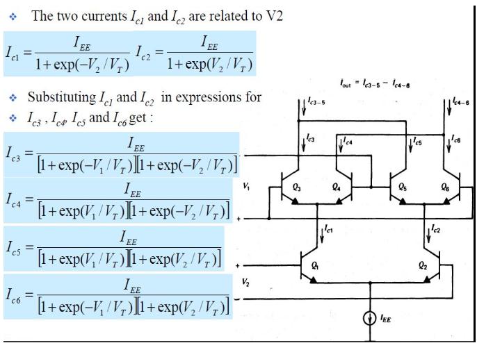
110 Introduction
111 MULTIPLIERS A multiple produces an output V0, which is proportional to the product of two inputs Vx and Vy. That is, V0 = K Vx Vy where K is the scaling factor that is usually maintained as (1/10) V-1 There are various methods available for performing analog multiplication. Four of such techniques, namely, 1. Logarithmic summing technique 2. Pulse height/width modulation Technique 3. Variable trans conductance Technique 4. Multiplication using Gilbert cell and 5. Multiplication using variable trans conductance technique.
112 Terminologies associated voltage of the multiplier characteristics Accuracy: This specifies the derivation of the actual output from the ideal output, for any combination of X and Y inputs falling within the permissible operating range of the multiplier. Linearity: This defines the accuracy of the multiplier. It represents the maximum percentage derivation from the ideal straight line output. An error surface is formed by plotting the output for different combinations of X and Y inputs. The Linearity Error can be defined as the maximum absolute derivation of the error surface. This linearity error imposes a lower limit on the multiplier accuracy.
113 ..CONTD Squaring Mode Accuracy: The Square law curve is obtained with both the X and Y inputs connected together and applied with the same input signal. The maximum derivation of the output voltage from an ideal square law curve expresses the squaring mode accuracy.
114 ..CONTD Bandwidth: The Bandwidth indicates the operating capability of an analog multiplier at higher frequency values. Small signal 3 db bandwidth defines the frequency f0 at which the output reduces by 3dB from its low frequency value for a constant input voltage. This is identified individually for the X and Y input channels normally. The transconductance bandwidth represents the frequency at which the transconductance of the multiplier drops by 3dB of its low frequency value. This characteristics defines the application frequency ranges when used for phase detection or AM detection. Quadrant: The quadrant defines the applicability of the circuit for bipolar signals at its inputs. First quadrant device accepts only positive input signals, the two quadrant device accepts one bipolar signal and one unipolar signal and the four quadrant device accepts two bipolar signals.
115 Logarithmic summing Technique: This technique uses the relationship lnvx + lnvy =ln(vxvy) Logarithmic multiplier has low accuracy and high temperature instability. This method is applicable only to positive values of Vx and Vy. this type of multiplier is restricted to one quadrant operation only.
116 Pulse Height/ Width Modulation Technique: V z = K z T = K z At=Vx Vy/Kx K

117 Multiplier using Emitter coupled Transistor pair
118 ..CONTD EC6404-LINEAR INTEGRATED CIRCUITS-ECE DEPT-SVCE
119
120
121
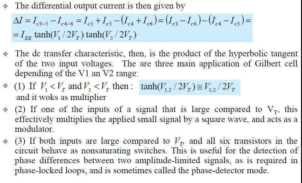
122
123


124
125
126 Variable Transconductance Technique: V0 = gm R L Vx = (Vy/VTRE)VxRL =(Vx Vy R L /V t R e
127 Four Quadrant Variable transconductance multiplier The four quadrant operation indicates that the output voltage is directly proportional to the product of the two input voltages regardless of the polarity of the inputs and such multipliers can be operated in all the four quadrants of operation.
128 Analog Multiplier ICs Analog multiplier is a circuit whose output voltage at any instant is proportional to the product instantaneous value of two individual input voltages. The important applications----multiplication, division, squaring and square rooting of signals, modulation and demodulation. These analog multipliers are available as integrated circuits consisting of op-amps and other circuit elements. V0 =VxVy/10
129 Multiplier quadrants: The transfer characteristics of a typical four-quadrant multiplier is shown in figure. Both the inputs can be positive or negative to obtain the corresponding output as shown in the transfer characteristics.
130 Applications of Multiplier ICs: The multiplier ICs are used for the following purposes: 1. Voltage Squarer 2. Frequency doubler 3. Voltage divider 4. Square rooter 5. Phase angle detector 6. Rectifier
131 Voltage Squarer: Figure shows the multiplier IC connected as a squaring circuit. The inputs can be positive or negative, represented by any corresponding voltage level between 0 and 10V. The input voltage Vi to be squared is simply connected to both the input terminals, and hence we have, Vx = Vy = Vi and the output is V0 = K Vi 2. The circuit thus performs the squaring operation. This application can be extended for frequency doubling applications.
132 Frequency doubler A sine-wave signal Vi has a peak amplitude of Av and frequency of fhz. Assuming a peak amplitude Av of 5V and frequency f of 10KHz, V0 = cos2π(20000)t. The first term represents the dc term of 1.25V peak amplitude. The output waveforms ripples with twice the input frequency in the rectified output of the input signal. This forms the principle of application of analog multiplier as rectifier of ac signals. The dc component of output V0 can be removed by connecting a 1μF coupling capacitor between the output terminal and a load resistor, across which the output can be observed.
133 Frequency doubler
134 Voltage Divider
135 Phase angle Detector EC6404-LINEAR INTEGRATED CIRCUITS-ECE DEPT-SVCE
136 PHASE LOCKED LOOP
137 PLL
138 PLL
139 PLL
140 PLL- construction and operation The phase detector or comparator compares the input frequency fs with feedback frequency fo. The output of the phase detector is proportional to the phase difference between fs & fo. The output of the phase detector is a dc voltage & therefore is often referred to as the error voltage. LPF removes the high frequency noise and produces a dc level. The high frequency component (fs + fo) is removed by the low pass filter The output frequency of VCO is directly proportional to the dc level. The VCO frequency is compared with input frequency and adjusted until it is equal to the input frequencies. PLL goes through 3 states, i) free running ii) Capture iii) Phase lock. Before the input is applied, the PLL is in free running state. Once the input frequency is applied the VCO frequency starts to change and PLL is said to be in the capture mode. The VCO frequency continuous to change until it equals the input frequency and the PLL is in phase lock mode. When Phase locked, the loop tracks any change in the input frequency through its repetitive action.
141 PLL The phase detector is basically a multiplier and produces the sum (fs + fo) and difference (fs - fo) components at its output. The high frequency component (fs + fo) is removed by the low pass filter and the difference frequency component is amplified then applied as control voltage vc to VCO. The signal vc shifts the VCO frequency in a direction to reduce the frequency difference between fs and fo. Once this action starts, we say that the signal is in the capture range. The VCO continues to change frequency till its output frequency is exactly the same as the input signal frequency. The circuit is then said to be locked. Once locked, the output frequency fo of VCO is identical to fs except for a finite phase difference φ. This phase difference φ generates a corrective control voltage vc to shift the VCO frequency from f0 to fs and thereby maintain the lock. Once locked,pll tracks the frequency changes of the input signal. Thus, a PLL goes through three stages (i)free running, (ii) capture and (iii) locked or tracking. Pull-in Capture time: range: the total the range time taken of frequencies by the PLL over to establish which the lock PLL is can called acquire pull-in lock with an input signal is called the capture range. This parameter is also expressed as percentage of fo.
142 Low Pass filter The function of the LPF is to remove the high frequency components in the output of the phase detector and to remove the high frequency noise. LPF controls the characteristics of the phase locked loop. i.e, capture range, lock ranges, bandwidth Lock range(tracking range):the lock range is defined as the range of frequencies over which the PLL system follows the changes in the input frequency fin. Capture range:capture range is the frequency range in which the PLL acquires phase lock. Capture range is always smaller than the lock range. Filter Bandwidth:Filter Bandwidth is reduced, its response time increases. However reduced Bandwidth reduces the capture range of the PLL. Reduced Bandwidth helps to keep the loop in lock through momentary losses of signal and also minimizes noise.

143 Voltage Controlled Oscillator (VCO) The third section of PLL is the VCO; it generates an output frequency that is directly proportional to its input voltage. Voltage controlled oscillator A voltage controlled oscillator is an oscillator circuit in which the frequency of oscillations can be controlled by an externally applied voltage The maximum output frequency of NE/SE 566 is 500 Khz.
144 Equations
145
146 Monilithic VCO-IC 566
147 MONOLITHIC PHASE LOCKED LOOPS (PLL IC 565) Pin Configuration of PLL IC 565:
148 Block Diagram
149 IC565 The signetics NE/SE 560 series is monolithic phase locked loops. The SE/NE 560, 561, 562, 564, 565 & 567 differ mainly in operating frequency range, poser supply requirements & frequency & bandwidth adjustment ranges. The important electrical characteristics of the 565 PLL are, Operating frequency range: 0.001Hz to 500 Khz. Operating voltage range: ±6 to ±12v Input level required for tracking: 10mv rms min to 3 Vpp max Input impedance: 10 K ohms typically. Output sink current: 1mA Output source current: 10 ma The center frequency of the PLL is determined by the free running frequency of the VCO, which is given by where R1&C1 are an external resistor & a capacitor connected to pins 8 & 9.
150 IC565 The lock range fl & capture range fc of PLL is given by,

151 Applications of PLL-IC 1.Frequency Multiplier
152 2.FSK Demodulator
153 FSK Demodulator The output of 555 FSK generator is applied to the 565 FSK demodulator. Capacitive coupling is used at the input to remove dc line. At the input of 565, the loop locks to the input frequency & tracks it between the 2 frequencies. R1 & C1 determine the free running frequency of the VCO, 3 stage RC ladder filter is used to remove the carrier component from the output.
154 3.AM Demodulation
155 4.Frequency multiplication/division:

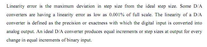
156 5.Frequency Synthesizer
157 Analog to Digital & Digital to Analog converters UNIT-IV
158 Analog Signals Analog signals directly measurable quantities in terms of some other quantity Examples: Thermometer mercury height rises as temperature rises Car Speedometer Needle moves farther right as you accelerate Stereo Volume increases as you turn the knob.
159 Digital Signals Digital Signals have only two states. For digital computers, we refer to binary states, 0 and 1. 1 can be on, 0 can be off. Examples: Light switch can be either on or off Door to a room is either open or closed
160 Examples of A/D Applications Microphones - take your voice varying pressure waves in the air and convert them into varying electrical signals Strain Gages - determines the amount of strain (change in dimensions) when a stress is applied Thermocouple temperature measuring device converts thermal energy to electric energy Voltmeters Digital Multimeters
161 D/A converter (DAC)
162 The Ideal Transfer Function (DAC) The DAC theoretical ideal transfer function would also be a straight line with an infinite number of steps but practically it is a series of points that fall on the ideal straight line as shown in Figure
163 Specifications of DAC Static errors, that is those errors that affect the accuracy of the converter when it is converting static (dc) signals, can be completely described by just four terms. These are : offset error, gain error, integral nonlinearity and differential nonlinearity. Each can be expressed in LSB units or sometimes as a percentage of the FSR

164 Offset Error - DAC For a DAC it is the step value when the digital input is zero. This error affects all codes by the same amount and can usually be compensated for by a trimming process. If trimming is not possible, this error is referred to as the zero-scale error.

165 Gain Error - DAC For a DAC it is the step value when the digital input is full scale. This error represents a difference in the slope of the actual and ideal transfer functions This error can also usually be adjusted to zero by trimming.
 and the ideal value of 1 LSB.")
166 Differential Nonlinearity (DNL) Error - DAC The differential nonlinearity error shown in Figure is the difference between an actual step height (for a DAC) and the ideal value of 1 LSB. Therefore if the step height is exactly 1 LSB, then the differential nonlinearity error is zero
167 Integral Nonlinerity (INL) Error - DAC - The name integral nonlinearity derives from the fact that the summation of the differential nonlinearities from the bottom up to a particular step, determines the value of the integral nonlinearity at that step.
168 Absolute Accuracy (Total) Error -DAC-
169
170 Accuracy
171 Linearity Monotonicity
172 Binary weighted Resistor DAC
173 4-bit Binary weighted Resistor DAC

174 Binary weighted Resistor DAC
175 Weighted Sum DAC One way to achieve D/A conversion is to use a summing amplifier. This approach is not satisfactory for a large number of bits because it requires too much precision in the summing resistors. This problem is overcome in the R-2R network DAC.

176 R-2R Ladder type DAC

177 R-2R Ladder DAC
178 R-2R Ladder DAC The summing amplifier with the R-2R ladder of resistances shown produces the output where the D's take the value 0 or 1. The digital inputs could be TTL voltages which close the switches on a logical 1 and leave it grounded for a logical 0. This is illustrated for 4 bits, but can be extended to any number with just the resistance values R and 2R.
179 R-2R Ladder DAC
180 R-2R Ladder DAC
181 Inverted or Current Mode DAC
182 Voltage Mode DAC
183 Switches for DAC Switches using Over-driven Emitter Followers Switches using MOS Transistor-Totem Pole MOSFET switch and CMOS Inverter Switch CMOS Switch for Multiplying type DACs CMOS Transmission gate switches
184 Series Sampling
185 High Speed Sample & Hold circuit
186 Switched op-amp based Sample and Hold Circuit
187 Sample and Hold circuit with MOSFET as a switch
188 Analog to Digital Converters

189 The offset error is efined as the difference between the nominal and actual offset points. Offset Error - ADC

190 Gain Error - ADC The gain error is defined as the difference between the nominal and actual gain points on the transfer function after the offset error has been corrected to zero. For an ADC, the gain point is the midstep value when the digital output is full scale,

191 Differential Nonlinearity (DNL) Error - ADC DNL is the difference between an actual step width (for an ADC) and the ideal value of 1 LSB. Therefore if the step width is exactly 1 LSB, then the differential nonlinearity error is zero. If the DNL exceeds 1 LSB nonmonotonic (this means that the magnitude of the output gets smaller for an increase in the magnitude of the input) If the DNL error of 1 LSB there is also a possibility that there can be missing codes i.e., one or more of the possible 2n binary codes are never output.

192 Integral Nonlinerity (INL) Error - ADC The integral nonlinearity error shown in Figure is the deviation of the values on the actual transfer function from a straight line. This straight line can be either a best straight line which is drawn so as to minimize these deviations or it can be a line drawn between the end points of the transfer function once the gain and offset errors have been nullified (end-point linearity )

193 Absolute Accuracy (Total) Error ADC The absolute accuracy or total error of an ADC as shown in Figure is the maximum value of the difference between an analog value and the ideal midstep value. It includes offset, gain, and integral linearity errors and also the quantization error in the case of an ADC
194 Resolution

195 Flash type ADC
196 Flash ADC Circuit
197 Flash ADC Circuit Advantages Simplest in terms of operational theory Most efficient in terms of speed, very fast limited only in terms of comparator and gate propagation delays Disadvantages Lower resolution Expensive For each additional output bit, the number of comparators is doubled i.e. for 8 bits, 256 comparators needed
198 Successive Approximation ADC A Successive Approximation Register (SAR) is added to the circuit Instead of counting up in binary sequence, this register counts by trying all values of bits starting with the MSB and finishing at the LSB. The register monitors the comparators output to see if the binary count is greater or less than the analog signal input and adjusts the bits accordingly
199 Successive Approximation ADC
200 Successive Approximation ADC Circuit
201 Successive Approximation Example 10 bit resolution or V of Vref Vin=.6 volts Vref=1volts Find the digital value of Vin
202 Successive Approximation MSB (bit 9) Divided V ref by 2 Compare V ref /2 with V in If V in is greater than V ref /2, turn MSB on (1) If V in is less than V ref /2, turn MSB off (0) V in =0.6V and V=0.5 Since V in >V, MSB = 1 (on)
203 Successive Approximation Next Calculate MSB-1 (bit 8) Compare V in =0.6 V to V=V ref /2 + V ref /4= =0.75V Since 0.6<0.75, MSB is turned off Calculate MSB-2 (bit 7) Go back to the last voltage that caused it to be turned on (Bit 9) and add it to V ref /8, and compare with V in Compare V in with (0.5+V ref /8)=0.625 Since 0.6<0.625, MSB is turned off
 and add it to V ref /16, and compare it to V in Compare V in to V= 0.5 + V ref /16= 0.5625 Since 0.6>0.")
204 Successive Approximation Calculate the state of MSB-3 (bit 6) Go to the last bit that caused it to be turned on (In this case MSB-1) and add it to V ref /16, and compare it to V in Compare V in to V= V ref /16= Since 0.6>0.5625, MSB-3=1 (turned on)
205 Successive Approximation This process continues for all the remaining bits.
206 Successive Approximation ADC Advantages Disadvantages Capable of high speed and reliable Medium accuracy compared to other ADC types Good tradeoff between speed and cost Higher resolution successive approximation ADC s will be slower Speed limited to ~5Msps Capable of outputting the binary number in serial (one bit at a time) format.
207 Integrating ADC


208 Dual Slope Converter V in t FIX t meas t The sampled signal charges a capacitor for a fixed amount of time By integrating over time, noise integrates out of the conversion Then the ADC discharges the capacitor at a fixed rate with the counter counts the ADC s output bits. A longer discharge time results in a higher count
209 Dual Slope Converter Advantages Input signal is averaged Greater noise immunity than other ADC types High accuracy Disadvantages Slow High precision external components required to achieve accuracy
210 A/D using Voltage to Time conversion
211 ADC Types Comparison Dual Slope ADC Resolution Comparison Flash Successive Approx Sigma-Delta Resolution (Bits) Type Speed (relative) Cost (relative) Dual Slope Slow Med Flash Very Fast High Successive Appox Medium Fast Low Sigma-Delta Slow Low
212 Analog Switches
213 Analog Switches
214 Oversampling A/D converters
215
216
217 UNIT-V SPECIAL FUNCTION ICS
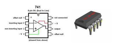
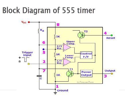
218 555 Timer The 555 timer IC is an integrated circuit (chip) used in a variety of timer, pulse generation, and oscillator applications. The 555 is used to provide time delays, as an oscillator, and as a flip-flop element. It gets its name from the three 5k ohm resistors which give the two comparators reference voltage. Depending on the manufacturer, the standard 555 package includes 25 transistors, 2 diodes and 15 resistors on a silicon chip installed in an 8-PIN DIP (Dual in-line) package.
219
220
221
222
223
224
225
226
227
228
229
230
231
232
233
234
235
236
237
238
239
240
241
242 Tuned Amplifier
243
244
245
246
247
248
249
250
251
252
253
254
255 Video Amplifiers The NE592 is a monolithic, two-stage, differential output, wideband video amplifier. It offers fixed gains of 100 and 400 without external components and adjustable gains from 400 to 0 with one external resistor. The input stage has been designed so that with the addition of a few external reactive elements between the gain select terminals, the circuit can function as a high-pass, low-pass, or band-pass filter. This feature makes the circuit ideal for use as a video or pulse amplifier in communications, magnetic memories, display, video recorder systems, and floppy disk head amplifiers. Now available in an 8-pin version with fixed gain of 400 without external components and adjustable gain from 400 to 0 with one external resistor
256 Block Diagram
257 Features and Applications Features : 120 MHz Unity Gain Bandwidth Adjustable Gains from 0 to 400 Adjustable Pass Band No Frequency Compensation Required Wave Shaping with Minimal External Components Applications : Floppy Disk Head Amplifier Pulse Amplifier in Communications Magnetic Memory andvideo Recorder Systems
258 Voltage Frequency Converter Circuit
259 Frequency Voltage Converter Circuit
260 Frequency to Voltage Converter - Circuit
261 Sources of Noise in Op-amp Thermal noise - Brownian motion of atoms, molecules, ions. Shot noise random movement of electrons or holes across a Pnjunction Transmit time noise Propagation time of current carriers causes noise, especially at high frequencies Quantization noise

262 Low Noise Op-amps

263 Op-amp Noise Analysis
Analog to Digital Converters
 Analog to Digital Converters By: Byron Johns, Danny Carpenter Stephanie Pohl, Harry Bo Marr http://ume.gatech.edu/mechatronics_course/fadc_f05.ppt (unless otherwise marked) Presentation Outline Introduction:
UNIT III ANALOG MULTIPLIER AND PLL
 UNIT III ANALOG MULTIPLIER AND PLL PART A (2 MARKS) 1. What are the advantages of variable transconductance technique? [AUC MAY 2012] Good Accuracy Economical Simple to integrate Reduced error Higher bandwidth
LINEAR IC APPLICATIONS
 1 B.Tech III Year I Semester (R09) Regular & Supplementary Examinations December/January 2013/14 1 (a) Why is R e in an emitter-coupled differential amplifier replaced by a constant current source? (b)
PHYS225 Lecture 22. Electronic Circuits
 PHYS225 Lecture 22 Electronic Circuits Last lecture Digital to Analog Conversion DAC Converts digital signal to an analog signal Computer control of everything! Various types/techniques for conversion
 VALLIAMMAI ENGINEERING COLLEGE SRM Nagar, Kattankulathur 603 203. DEPARTMENT OF ELECTRONICS & COMMUNICATION ENGINEERING QUESTION BANK SUBJECT : EC6404 LINEAR INTEGRATED CIRCUITS SEM / YEAR: IV / II year
Question Paper Code: 21398
 Reg. No. : Question Paper Code: 21398 B.E./B.Tech. DEGREE EXAMINATION, MAY/JUNE 2013 Fourth Semester Electrical and Electronics Engineering EE2254 LINEAR INTEGRATED CIRCUITS AND APPLICATIONS (Regulation
Summer 2015 Examination
 Summer 2015 Examination Subject Code: 17445 Model Answer Important Instructions to examiners: 1) The answers should be examined by key words and not as word-to-word as given in the model answer scheme.
The steeper the phase shift as a function of frequency φ(ω) the more stable the frequency of oscillation
 the more stable the frequency of oscillation") It should be noted that the frequency of oscillation ω o is determined by the phase characteristics of the feedback loop. the loop oscillates at the frequency for which the phase is zero The steeper the
It should be noted that the frequency of oscillation ω o is determined by the phase characteristics of the feedback loop. the loop oscillates at the frequency for which the phase is zero The steeper the
B.E. SEMESTER III (ELECTRICAL) SUBJECT CODE: X30902 Subject Name: Analog & Digital Electronics
 SUBJECT CODE: X30902 Subject Name: Analog & Digital Electronics") B.E. SEMESTER III (ELECTRICAL) SUBJECT CODE: X30902 Subject Name: Analog & Digital Electronics Sr. No. Date TITLE To From Marks Sign 1 To verify the application of op-amp as an Inverting Amplifier 2 To
B.E. SEMESTER III (ELECTRICAL) SUBJECT CODE: X30902 Subject Name: Analog & Digital Electronics Sr. No. Date TITLE To From Marks Sign 1 To verify the application of op-amp as an Inverting Amplifier 2 To
Operational Amplifiers
 Operational Amplifiers Table of contents 1. Design 1.1. The Differential Amplifier 1.2. Level Shifter 1.3. Power Amplifier 2. Characteristics 3. The Opamp without NFB 4. Linear Amplifiers 4.1. The Non-Inverting
DMI COLLEGE OF ENGINEERING
 DMI COLLEGE OF ENGINEERING DEPARTMENT OF ELECTRONICS & COMMUNICATION ENGINEERING EC8453 - LINEAR INTEGRATED CIRCUITS Question Bank (II-ECE) UNIT I BASICS OF OPERATIONAL AMPLIFIERS PART A 1.Mention the
LESSON PLAN. SUBJECT: LINEAR IC S AND APPLICATION NO OF HOURS: 52 FACULTY NAME: Mr. Lokesh.L, Hema. B DEPT: ECE. Portions to be covered
 LESSON PLAN SUBJECT: LINEAR IC S AND APPLICATION SUB CODE: 15EC46 NO OF HOURS: 52 FACULTY NAME: Mr. Lokesh.L, Hema. B DEPT: ECE Class# Chapter title/reference literature Portions to be covered MODULE I
KINGS COLLEGE OF ENGINEERING* DEPARTMENT OF ELECTRONICS AND COMMUNICATION ENGINEERING QUESTION BANK
 KINGS COLLEGE OF ENGINEERING* DEPARTMENT OF ELECTRONICS AND COMMUNICATION ENGINEERING QUESTION BANK SUB.NAME : LINEAR INTEGRATED CIRCUITS SUB CODE: EC1254 YEAR / SEMESTER : II / IV UNIT- I IC FABRICATION
INSTITUTE OF AERONAUTICAL ENGINEERING (Autonomous) Dundigal, Hyderabad
 Dundigal, Hyderabad") 1 P a g e INSTITUTE OF AERONAUTICAL ENGINEERING (Autonomous) Dundigal, Hyderabad - 500 043 ELECTRONICS AND COMMUNICATION ENGINEERING TUTORIAL QUESTION BANK Name : INTEGRATED CIRCUITS APPLICATIONS Code
1 P a g e INSTITUTE OF AERONAUTICAL ENGINEERING (Autonomous) Dundigal, Hyderabad - 500 043 ELECTRONICS AND COMMUNICATION ENGINEERING TUTORIAL QUESTION BANK Name : INTEGRATED CIRCUITS APPLICATIONS Code
St.MARTIN S ENGINEERING COLLEGE
 St.MARTIN S ENGINEERING COLLEGE Dhulapally, Kompally, Secunderabad-500014. Branch Year&Sem Subject Name : Electrical and Electronics Engineering : III B. Tech I Semester : IC Applications OBJECTIVES QUESTION
Transistor Design & Analysis (Inverter)
") Experiment No. 1: DIGITAL ELECTRONIC CIRCUIT Transistor Design & Analysis (Inverter) APPARATUS: Transistor Resistors Connecting Wires Bread Board Dc Power Supply THEORY: Digital electronics circuits operate
Experiment No. 1: DIGITAL ELECTRONIC CIRCUIT Transistor Design & Analysis (Inverter) APPARATUS: Transistor Resistors Connecting Wires Bread Board Dc Power Supply THEORY: Digital electronics circuits operate
LIC & COMMUNICATION LAB MANUAL
 LIC & Communication Lab Manual LIC & COMMUNICATION LAB MANUAL FOR V SEMESTER B.E (E& ( E&C) (For private circulation only) NAME: DEPARTMENT OF ELECTRONICS & COMMUNICATION SRI SIDDHARTHA INSTITUTE OF TECHNOLOGY
UNIT-I CIRCUIT CONFIGURATION FOR LINEAR
 UNIT-I CIRCUIT CONFIGURATION FOR LINEAR ICs 2 marks questions 1.Mention the advantages of integrated circuits. *Miniaturisation and hence increased equipment density. *Cost reduction due to batch processing.
R (a) Explain characteristics and limitations of op-amp comparators. (b) Explain operation of free running Multivibrator using op-amp.
 Explain characteristics and limitations of op-amp comparators. (b) Explain operation of free running Multivibrator using op-amp.") Set No: 1 1. (a) Draw the equivalent circuits of emitter coupled differential amplifier from which calculate Ad. (b) Draw the block diagram of four stage cascaded amplifier. Explain the function of each
Set No: 1 1. (a) Draw the equivalent circuits of emitter coupled differential amplifier from which calculate Ad. (b) Draw the block diagram of four stage cascaded amplifier. Explain the function of each
EC6404-LINEAR INTEGRATED CIRCUITS Question bank UNIT-I PART-A 1. What are the advantages of an IC over discrete components?
 EC6404-LINEAR INTEGRATED CIRCUITS Question bank UNIT-I PART-A 1. What are the advantages of an IC over discrete components?(apr-2014)(apr- 2013,Nov-2014) 2. State an Monolitihic ICs.(Apr-2010,Nov-2014)
HIGH LOW Astable multivibrators HIGH LOW 1:1
 1. Multivibrators A multivibrator circuit oscillates between a HIGH state and a LOW state producing a continuous output. Astable multivibrators generally have an even 50% duty cycle, that is that 50% of
For input: Peak to peak amplitude of the input = volts. Time period for 1 full cycle = sec
 Inverting amplifier: [Closed Loop Configuration] Design: A CL = V o /V in = - R f / R in ; Assume R in = ; Gain = ; Circuit Diagram: RF +10V F.G ~ + Rin 2 3 7 IC741 + 4 6 v0-10v CRO Model Graph Inverting
VALLIAMMAI ENGINEERING COLLEGE SRM Nagar, Kattankulathur DEPARTMENT OF ELECTRONICS AND COMMUNICATION ENGINEERING QUESTION BANK IV SEMESTER
 VALLIAMMAI ENGINEERING COLLEGE SRM Nagar, Kattankulathur 603 203 DEPARTMENT OF ELECTRONICS AND COMMUNICATION ENGINEERING QUESTION BANK IV SEMESTER EC6404 LINEAR INTEGRATED CIRCUITS Regulation 2013 Academic
PROPOSED SCHEME OF COURSE WORK
 PROPOSED SCHEME OF COURSE WORK Course Details: Course Title : LINEAR AND DIGITAL IC APPLICATIONS Course Code : 13EC1146 L T P C : 4 0 0 3 Program: : B.Tech. Specialization: : Electrical and Electronics
Speed Control of DC Motor Using Phase-Locked Loop
 Speed Control of DC Motor Using Phase-Locked Loop Authors Shaunak Vyas Darshit Shah Affiliations B.Tech. Electrical, Nirma University, Ahmedabad E-mail shaunak_vyas1@yahoo.co.in darshit_shah1@yahoo.co.in
COMPARATOR CHARACTERISTICS The important characteristics of a comparator are these: 1. Speed of operation 2. Accuracy 3. Compatibility of output
 SCHMITT TRIGGER (regenerative comparator) Schmitt trigger is an inverting comparator with positive feedback. It converts an irregular-shaped waveform to a square wave or pulse, also called as squaring
LM13600 Dual Operational Transconductance Amplifiers with Linearizing Diodes and Buffers
 LM13600 Dual Operational Transconductance Amplifiers with Linearizing Diodes and Buffers General Description The LM13600 series consists of two current controlled transconductance amplifiers each with
SYLLABUS. osmania university CHAPTER - 1 : OPERATIONAL AMPLIFIER CHAPTER - 2 : OP-AMP APPLICATIONS ARATORS AND CONVERTERS
 Contents i SYLLABUS osmania university UNIT - I CHAPTER - 1 : OPERATIONAL AMPLIFIER Operational Amplifiers-Characteristics, Open Loop Voltage Gain, Output Impedance, Input Impedance, Common Mode Rejection
About the Tutorial. Audience. Prerequisites. Copyright & Disclaimer. Linear Integrated Circuits Applications
 About the Tutorial Linear Integrated Circuits are solid state analog devices that can operate over a continuous range of input signals. Theoretically, they are characterized by an infinite number of operating
Analog I/O. ECE 153B Sensor & Peripheral Interface Design Winter 2016
 Analog I/O ECE 153B Sensor & Peripheral Interface Design Introduction Anytime we need to monitor or control analog signals with a digital system, we require analogto-digital (ADC) and digital-to-analog
Dev Bhoomi Institute Of Technology Department of Electronics and Communication Engineering PRACTICAL INSTRUCTION SHEET REV. NO. : REV.
 Dev Bhoomi Institute Of Technology Department of Electronics and Communication Engineering PRACTICAL INSTRUCTION SHEET LABORATORY MANUAL EXPERIMENT NO. ISSUE NO. : ISSUE DATE: July 200 REV. NO. : REV.
GATE: Electronics MCQs (Practice Test 1 of 13)
") GATE: Electronics MCQs (Practice Test 1 of 13) 1. Removing bypass capacitor across the emitter leg resistor in a CE amplifier causes a. increase in current gain b. decrease in current gain c. increase
GATE: Electronics MCQs (Practice Test 1 of 13) 1. Removing bypass capacitor across the emitter leg resistor in a CE amplifier causes a. increase in current gain b. decrease in current gain c. increase
BINARY AMPLITUDE SHIFT KEYING
 BINARY AMPLITUDE SHIFT KEYING AIM: To set up a circuit to generate Binary Amplitude Shift keying and to plot the output waveforms. COMPONENTS AND EQUIPMENTS REQUIRED: IC CD4016, IC 7474, Resistors, Zener
FIRSTRANKER. 1. (a) What are the advantages of the adjustable voltage regulators over the fixed
 What are the advantages of the adjustable voltage regulators over the fixed") Code No: 07A51102 R07 Set No. 2 1. (a) What are the advantages of the adjustable voltage regulators over the fixed voltage regulators. (b) Differentiate betweenan integrator and a differentiator. [8+8]
Code No: 07A51102 R07 Set No. 2 1. (a) What are the advantages of the adjustable voltage regulators over the fixed voltage regulators. (b) Differentiate betweenan integrator and a differentiator. [8+8]
Figure 1: Closed Loop System
 SIGNAL GENERATORS 3. Introduction Signal sources have a variety of applications including checking stage gain, frequency response, and alignment in receivers and in a wide range of other electronics equipment.
 1 2 B.E./B.Tech. DEGREE EXAMINATION, NOVEMBER/DECEMBER 2010 Fourth Semester Electrical and Electronics Engineering EE 2254 LINEAR INTEGRATED CIRCUITS AND APPLICATIONS (Common to Instrumentation and Control
Gechstudentszone.wordpress.com
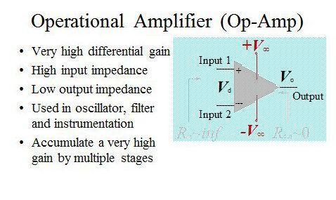
 8.1 Operational Amplifier (Op-Amp) UNIT 8: Operational Amplifier An operational amplifier ("op-amp") is a DC-coupled high-gain electronic voltage amplifier with a differential input and, usually, a single-ended
UNITII. Other LICs and Data Converters
 UNITII Other LICs and Data Converters Other LICs and Data Converters: 555 timer Block diagram and features Astable Multivibrator Applications - Square wave oscillator, Ramp generator, Triangular waveform
Chapter 2 Signal Conditioning, Propagation, and Conversion
 09/0 PHY 4330 Instrumentation I Chapter Signal Conditioning, Propagation, and Conversion. Amplification (Review of Op-amps) Reference: D. A. Bell, Operational Amplifiers Applications, Troubleshooting,
Let us consider the following block diagram of a feedback amplifier with input voltage feedback fraction,, be positive i.e. in phase.
 P a g e 2 Contents 1) Oscillators 3 Sinusoidal Oscillators Phase Shift Oscillators 4 Wien Bridge Oscillators 4 Square Wave Generator 5 Triangular Wave Generator Using Square Wave Generator 6 Using Comparator
Phase-locked loop PIN CONFIGURATIONS
 NE/SE DESCRIPTION The NE/SE is a versatile, high guaranteed frequency phase-locked loop designed for operation up to 0MHz. As shown in the Block Diagram, the NE/SE consists of a VCO, limiter, phase comparator,
Scheme I Sample Question Paper
 Sample Question Paper Marks : 70 Time: 3 Hrs. Q.1) Attempt any FIVE of the following. 10 Marks a) Classify configuration of differential amplifier. b) Draw equivalent circuit of an OPAMP c) Suggest and
ASTABLE MULTIVIBRATOR
 555 TIMER ASTABLE MULTIIBRATOR MONOSTABLE MULTIIBRATOR 555 TIMER PHYSICS (LAB MANUAL) PHYSICS (LAB MANUAL) 555 TIMER Introduction The 555 timer is an integrated circuit (chip) implementing a variety of
AC LAB ECE-D ecestudy.wordpress.com
 PART B EXPERIMENT NO: 1 AIM: PULSE AMPLITUDE MODULATION (PAM) & DEMODULATION DATE: To study Pulse Amplitude modulation and demodulation process with relevant waveforms. APPARATUS: 1. Pulse amplitude modulation
FSK DEMODULATOR / TONE DECODER
 FSK DEMODULATOR / TONE DECODER GENERAL DESCRIPTION The is a monolithic phase-locked loop (PLL) system especially designed for data communications. It is particularly well suited for FSK modem applications,
INTEGRATED CIRCUITS AND APPLICATIONS LAB MANUAL
 INTEGRATED CIRCUITS AND APPLICATIONS LAB MANUAL V SEMESTER Department of Electronics and communication Engineering Government Engineering College, Dahod-389151 http://www.gecdahod.ac.in/ L A B M A N U
Advantages of Analog Representation. Varies continuously, like the property being measured. Represents continuous values. See Figure 12.
 Analog Signals Signals that vary continuously throughout a defined range. Representative of many physical quantities, such as temperature and velocity. Usually a voltage or current level. Digital Signals
DEPARTMENT OF ELECTRONICS AND COMMUNICATION ENGINEERING QUESTION BANK
 DHANALAKSHMI SRINIVASAN COLLEGE OF ENGINEERING AND TECHNOLOGY ECR, MAMALLAPURAM CHENNAI-603104 DEPARTMENT OF ELECTRONICS AND COMMUNICATION ENGINEERING EC6404- LINEAR INTEGRATED CIRCUITS QUESTION BANK PREPARED
Difference between BJTs and FETs. Junction Field Effect Transistors (JFET)
") Difference between BJTs and FETs Transistors can be categorized according to their structure, and two of the more commonly known transistor structures, are the BJT and FET. The comparison between BJTs
Difference between BJTs and FETs Transistors can be categorized according to their structure, and two of the more commonly known transistor structures, are the BJT and FET. The comparison between BJTs
Government Polytechnic Muzaffarpur Name of the Lab: Applied Electronics Lab
 Government Polytechnic Muzaffarpur Name of the Lab: Applied Electronics Lab Subject Code: 1620408 Experiment-1 Aim: To obtain the characteristics of field effect transistor (FET). Theory: The Field Effect
Low Cost 10-Bit Monolithic D/A Converter AD561
 a FEATURES Complete Current Output Converter High Stability Buried Zener Reference Laser Trimmed to High Accuracy (1/4 LSB Max Error, AD561K, T) Trimmed Output Application Resistors for 0 V to +10 V, 5
SYLLABUS. osmania university UNIT - I UNIT - II UNIT - III CHAPTER - 4 : OPERATIONAL AMPLIFIER
 Contents i SYLLABUS osmania university UNIT - I CHAPTER - 1 : DIFFERENTIAL AMPLIFIERS Classification, DC and AC Analysis of Single/Dual Input Balanced and Unbalanced Output Configurations using BJTs. Level
Fig 1: The symbol for a comparator
 INTRODUCTION A comparator is a device that compares two voltages or currents and switches its output to indicate which is larger. They are commonly used in devices such as They are commonly used in devices
INTEGRATED CIRCUITS. AN109 Microprocessor-compatible DACs Dec
 INTEGRATED CIRCUITS 1988 Dec DAC products are designed to convert a digital code to an analog signal. Since a common source of digital signals is the data bus of a microprocessor, DAC circuits that are
P a g e 1. Introduction
 P a g e 1 Introduction 1. Signals in digital form are more convenient than analog form for processing and control operation. 2. Real world signals originated from temperature, pressure, flow rate, force
Multivibrators. Department of Electrical & Electronics Engineering, Amrita School of Engineering
 Multivibrators Multivibrators Multivibrator is an electronic circuit that generates square, rectangular, pulse waveforms. Also called as nonlinear oscillators or function generators. Multivibrator is basically
tyuiopasdfghjklzxcvbnmqwertyuiopas dfghjklzxcvbnmqwertyuiopasdfghjklzx cvbnmqwertyuiopasdfghjklzxcvbnmq
 qwertyuiopasdfghjklzxcvbnmqwertyui opasdfghjklzxcvbnmqwertyuiopasdfgh jklzxcvbnmqwertyuiopasdfghjklzxcvb nmqwertyuiopasdfghjklzxcvbnmqwer Instrumentation Device Components Semester 2 nd tyuiopasdfghjklzxcvbnmqwertyuiopas
explain its operation with clearly indicating the protection mechanisms indicated. [Marks 16] (Nov/dec 2010) Ic 741 Op Amp Of Output Stage Protection
![explain its operation with clearly indicating the protection mechanisms indicated. [Marks 16] (Nov/dec 2010) Ic 741 Op Amp Of Output Stage Protection](/thumbs/89/98803954.jpg "explain its operation with clearly indicating the protection mechanisms indicated. [Marks 16] (Nov/dec 2010) Ic 741 Op Amp Of Output Stage Protection") PANDIAN SARASWATH YADAV ENGINEERING COLLEGE ARASANOOR-SIVAGANGAI. DEPARTMENT OF ELECTRONICS AND COMMUNICATION ENGNIEERING EC6404-linear integrated circuits 16 MARK UNIVERSITY QUESTIONS WITH KEY UNIT-1
PANDIAN SARASWATH YADAV ENGINEERING COLLEGE ARASANOOR-SIVAGANGAI. DEPARTMENT OF ELECTRONICS AND COMMUNICATION ENGNIEERING EC6404-linear integrated circuits 16 MARK UNIVERSITY QUESTIONS WITH KEY UNIT-1
EE LINEAR INTEGRATED CIRCUITS AND APPLICATIONS TWO MARK QUESTIONS WITH ANSWERS UNIT-I CIRCUIT CONFIGURATION FOR LINEAR ICs
 EE6303 - LINEAR INTEGRATED CIRCUITS AND APPLICATIONS TWO MARK QUESTIONS WITH ANSWERS UNIT-I CIRCUIT CONFIGURATION FOR LINEAR ICs 1. Mention the advantages of integrated circuits. *Miniaturization and hence
Linear Integrated Circuits and Applications
 Dhanalakshmi Srinivasan Engineering College - Perambalur Department of EEE QUESTION BANK Linear Integrated Circuits and Applications UNIT-I ICs FABRICATION 1. Mention the advantages of integrated circuits.
An active filter offers the following advantages over a passive filter:
 ACTIVE FILTERS An electric filter is often a frequency-selective circuit that passes a specified band of frequencies and blocks or attenuates signals of frequencies outside this band. Filters may be classified
Concepts to be Reviewed
 Introductory Medical Device Prototyping Analog Circuits Part 3 Operational Amplifiers, http://saliterman.umn.edu/ Department of Biomedical Engineering, University of Minnesota Concepts to be Reviewed Operational
ICL MHz, Four Quadrant Analog Multiplier. Features. Ordering Information. Pinout. Functional Diagram. September 1998 File Number 2863.
 Semiconductor ICL80 September 998 File Number 28. MHz, Four Quadrant Analog Multiplier The ICL80 is a four quadrant analog multiplier whose output is proportional to the algebraic product of two input
Voltage-to-Frequency and Frequency-to-Voltage Converter ADVFC32
 a FEATURES High Linearity 0.01% max at 10 khz FS 0.05% max at 100 khz FS 0.2% max at 500 khz FS Output TTL/CMOS Compatible V/F or F/V Conversion 6 Decade Dynamic Range Voltage or Current Input Reliable
CHAPTER 6 DIGITAL INSTRUMENTS
 CHAPTER 6 DIGITAL INSTRUMENTS 1 LECTURE CONTENTS 6.1 Logic Gates 6.2 Digital Instruments 6.3 Analog to Digital Converter 6.4 Electronic Counter 6.6 Digital Multimeters 2 6.1 Logic Gates 3 AND Gate The
Quad 12-Bit Digital-to-Analog Converter (Serial Interface)
") Quad 1-Bit Digital-to-Analog Converter (Serial Interface) FEATURES COMPLETE QUAD DAC INCLUDES INTERNAL REFERENCES AND OUTPUT AMPLIFIERS GUARANTEED SPECIFICATIONS OVER TEMPERATURE GUARANTEED MONOTONIC OVER
Quad 1-Bit Digital-to-Analog Converter (Serial Interface) FEATURES COMPLETE QUAD DAC INCLUDES INTERNAL REFERENCES AND OUTPUT AMPLIFIERS GUARANTEED SPECIFICATIONS OVER TEMPERATURE GUARANTEED MONOTONIC OVER
LM13700 Dual Operational Transconductance Amplifiers with Linearizing Diodes and Buffers
 LM13700 Dual Operational Transconductance Amplifiers with Linearizing Diodes and Buffers General Description The LM13700 series consists of two current controlled transconductance amplifiers, each with
EE2254 LINEAR INTEGRATED CIRCUITS UNIT-I IC FABRICATION
 DEPARTMENT OF ELECTRICAL AND ELECTRONICS ENGINEERING Question bank EE2254 LINEAR INTEGRATED CIRCUITS UNIT-I IC FABRICATION 1. Mention the advantages of integrated circuits. 2. Write down the various processes
UNIT III Data Acquisition & Microcontroller System. Mr. Manoj Rajale
 UNIT III Data Acquisition & Microcontroller System Mr. Manoj Rajale Syllabus Interfacing of Sensors / Actuators to DAQ system, Bit width, Sampling theorem, Sampling Frequency, Aliasing, Sample and hold
SIR PADAMPAT SINGHANIA UNIVERSITY UDAIPUR Sample Question Paper for Ph.D. (Electronics & Communication Engineering) SPSAT 18
 SPSAT 18") INSTRUCTIONS SIR PADAMPAT SINGHANIA UNIVERSITY UDAIPUR Sample Question Paper for Ph.D. (Electronics & Communication Engineering) SPSAT 18 The test is 60 minutes long and consists of 40 multiple choice
INSTRUCTIONS SIR PADAMPAT SINGHANIA UNIVERSITY UDAIPUR Sample Question Paper for Ph.D. (Electronics & Communication Engineering) SPSAT 18 The test is 60 minutes long and consists of 40 multiple choice
OBJECTIVE TYPE QUESTIONS
 OBJECTIVE TYPE QUESTIONS Q.1 The breakdown mechanism in a lightly doped p-n junction under reverse biased condition is called (A) avalanche breakdown. (B) zener breakdown. (C) breakdown by tunnelling.
MODEL ANSWER SUMMER 17 EXAMINATION Subject Title: Linear Integrated Circuit Subject Code:
 MODEL ANSWER SUMMER 17 EXAMINATION Subject Title: Linear Integrated Circuit Subject Code: Important Instructions to examiners: 1) The answers should be examined by key words and not as word-to-word as
Figure 1.1 Mechatronic system components (p. 3)
") Figure 1.1 Mechatronic system components (p. 3) Example 1.2 Measurement System Digital Thermometer (p. 5) Figure 2.2 Electric circuit terminology (p. 13) Table 2.2 Resistor color band codes (p. 18) Figure
Figure 1.1 Mechatronic system components (p. 3) Example 1.2 Measurement System Digital Thermometer (p. 5) Figure 2.2 Electric circuit terminology (p. 13) Table 2.2 Resistor color band codes (p. 18) Figure
DIGITAL COMMUNICATIONS LAB
 DIGITAL COMMUNICATIONS LAB List of Experiments: 1. PCM Generation and Detection. 2. Differential Pulse Code modulation. 3. Delta modulation. 4. Time Division Multiplexing of 2band Limited Signals. 5. Frequency
LM13700 Dual Operational Transconductance Amplifiers with Linearizing Diodes and Buffers
 LM13700 Dual Operational Transconductance Amplifiers with Linearizing Diodes and Buffers General Description The LM13700 series consists of two current controlled transconductance amplifiers, each with
1 Signals and systems, A. V. Oppenhaim, A. S. Willsky, Prentice Hall, 2 nd edition, FUNDAMENTALS. Electrical Engineering. 2.
 1 Signals and systems, A. V. Oppenhaim, A. S. Willsky, Prentice Hall, 2 nd edition, 1996. FUNDAMENTALS Electrical Engineering 2.Processing - Analog data An analog signal is a signal that varies continuously.
1) Consider the circuit shown in figure below. Compute the output waveform for an input of 5kHz
 Consider the circuit shown in figure below. Compute the output waveform for an input of 5kHz") ) Consider the circuit shown in figure below. Compute the output waveform for an input of 5kHz Solution: a) Input is of constant amplitude of 2 V from 0 to 0. ms and 2 V from 0. ms to 0.2 ms. The output
) Consider the circuit shown in figure below. Compute the output waveform for an input of 5kHz Solution: a) Input is of constant amplitude of 2 V from 0 to 0. ms and 2 V from 0. ms to 0.2 ms. The output
TUTORIAL 283 INL/DNL Measurements for High-Speed Analog-to- Digital Converters (ADCs)
") Maxim > Design Support > Technical Documents > Tutorials > A/D and D/A Conversion/Sampling Circuits > APP 283 Maxim > Design Support > Technical Documents > Tutorials > High-Speed Signal Processing > APP
Maxim > Design Support > Technical Documents > Tutorials > A/D and D/A Conversion/Sampling Circuits > APP 283 Maxim > Design Support > Technical Documents > Tutorials > High-Speed Signal Processing > APP
Data Converters. Dr.Trushit Upadhyaya EC Department, CSPIT, CHARUSAT
 Data Converters Dr.Trushit Upadhyaya EC Department, CSPIT, CHARUSAT Purpose To convert digital values to analog voltages V OUT Digital Value Reference Voltage Digital Value DAC Analog Voltage Analog Quantity:
GOVERNMENT OF KARNATAKA KARNATAKA STATE PRE-UNIVERSITY EDUCATION EXAMINATION BOARD II YEAR PUC EXAMINATION MARCH-2013 SCHEME OF VALUATION
 GOVERNMENT OF KARNATAKA KARNATAKA STATE PRE-UNIVERSITY EDUCATION EXAMINATION BOARD II YEAR PUC EXAMINATION MARCH-03 SCHEME OF VALUATION Subject Code: 0 Subject: PART - A 0. What does the arrow mark indicate
(Refer Slide Time: 00:03:22)
") Analog ICs Prof. K. Radhakrishna Rao Department of Electrical Engineering Indian Institute of Technology, Madras Lecture - 27 Phase Locked Loop (Continued) Digital to Analog Converters So we were discussing
Analog ICs Prof. K. Radhakrishna Rao Department of Electrical Engineering Indian Institute of Technology, Madras Lecture - 27 Phase Locked Loop (Continued) Digital to Analog Converters So we were discussing
Department of Electronics & Telecommunication Engg. LAB MANUAL. B.Tech V Semester [ ] (Branch: ETE)
![Department of Electronics & Telecommunication Engg. LAB MANUAL. B.Tech V Semester [ ] (Branch: ETE)](/thumbs/86/93078052.jpg "Department of Electronics & Telecommunication Engg. LAB MANUAL. B.Tech V Semester [ ] (Branch: ETE)") Department of Electronics & Telecommunication Engg. LAB MANUAL SUBJECT:-DIGITAL COMMUNICATION SYSTEM [BTEC-501] B.Tech V Semester [2013-14] (Branch: ETE) KCT COLLEGE OF ENGG & TECH., FATEHGARH PUNJAB TECHNICAL
Department of Electronics & Telecommunication Engg. LAB MANUAL SUBJECT:-DIGITAL COMMUNICATION SYSTEM [BTEC-501] B.Tech V Semester [2013-14] (Branch: ETE) KCT COLLEGE OF ENGG & TECH., FATEHGARH PUNJAB TECHNICAL
CHADALAWADA RAMANAMMA ENGINEERING COLLEGE (AUTONOMOUS) Chadalawada Nagar, Renigunta Road, Tirupati
 Chadalawada Nagar, Renigunta Road, Tirupati") IC APPLICATIONS LABORATORY MANUAL Subject Code : 15A04507 Regulations : R15 Class : V Semester (ECE) CHADALAWADA RAMANAMMA ENGINEERING COLLEGE (AUTONOMOUS) Chadalawada Nagar, Renigunta Road, Tirupati 517
IC APPLICATIONS LABORATORY MANUAL Subject Code : 15A04507 Regulations : R15 Class : V Semester (ECE) CHADALAWADA RAMANAMMA ENGINEERING COLLEGE (AUTONOMOUS) Chadalawada Nagar, Renigunta Road, Tirupati 517
Lab 2 Revisited Exercise
 Lab 2 Revisited Exercise +15V 100k 1K 2N2222 Wire up led display Note the ground leads LED orientation 6.091 IAP 2008 Lecture 3 1 Comparator, Oscillator +5 +15 1k 2 V- 7 6 Vin 3 V+ 4 V o Notice that power
Function Generator Using Op Amp Ic 741 Theory
 Function Generator Using Op Amp Ic 741 Theory Note: Op-Amps ua741, LM 301, LM311, LM 324 & AD 633 may be used To design an Inverting Amplifier for the given specifications using Op-Amp IC 741. THEORY:
Dr.NNCE ECE/IVSEM LIC LAB-LM
 EC2258 - LINEAR INTEGRATED CIRCUITS LABORATORY LABORATORY MANUAL FOR IV SEMESTER B.E (ECE) ACADEMIC YEAR(2013-2014) (FOR PRIVATE CIRCULATION ONLY) ANNA UNIVERSITY CHENNAI-600 025 (REGULATION 2008) DEPARTMENT
Electronics A/D and D/A converters
 Electronics A/D and D/A converters Prof. Márta Rencz, Gábor Takács, Dr. György Bognár, Dr. Péter G. Szabó BME DED December 1, 2014 1 / 26 Introduction The world is analog, signal processing nowadays is
Specifying A D and D A Converters
 Specifying A D and D A Converters The specification or selection of analog-to-digital (A D) or digital-to-analog (D A) converters can be a chancey thing unless the specifications are understood by the
Introduction to IC-555. Compiled By: Chanakya Bhatt EE, IT-NU
 Introduction to IC-555 Compiled By: Chanakya Bhatt EE, IT-NU Introduction SE/NE 555 is a Timer IC introduced by Signetics Corporation in 1970 s. It is basically a monolithic timing circuit that produces
Basic Operational Amplifier Circuits
 Basic Operational Amplifier Circuits Comparators A comparator is a specialized nonlinear op-amp circuit that compares two input voltages and produces an output state that indicates which one is greater.
LAB MANUAL EC6412- LINEAR INTEGRATED CIRCUIT LABORATORY. Dharmapuri Regulation : 2013 Branch : B.E. ECE
 EC6412 LINEAR INTEGRATED CIRCUITS LABORATORY 1 Dharmapuri 636 703 LAB MANUAL Regulation : 2013 Branch Year & Semester : B.E. ECE : II Year / IV Semester EC6412- LINEAR INTEGRATED CIRCUIT LABORATORY EC6412
PHYS225 Lecture 18. Electronic Circuits
 PHYS225 Lecture 18 Electronic Circuits Oscillators and Timers Oscillators & Timers Produce timing signals to initiate measurement Periodic or single pulse Periodic output at known (controlled) frequency
ML4818 Phase Modulation/Soft Switching Controller
 Phase Modulation/Soft Switching Controller www.fairchildsemi.com Features Full bridge phase modulation zero voltage switching circuit with programmable ZV transition times Constant frequency operation
Devices and Op-Amps p. 1 Introduction to Diodes p. 3 Introduction to Diodes p. 4 Inside the Diode p. 6 Three Diode Models p. 10 Computer Circuit
 Contents p. v Preface p. ix Devices and Op-Amps p. 1 Introduction to Diodes p. 3 Introduction to Diodes p. 4 Inside the Diode p. 6 Three Diode Models p. 10 Computer Circuit Analysis p. 16 MultiSIM Lab
OSCILLATORS AND WAVEFORM-SHAPING CIRCUITS
 OSILLATORS AND WAVEFORM-SHAPING IRUITS Signals having prescribed standard waveforms (e.g., sinusoidal, square, triangle, pulse, etc). To generate sinusoidal waveforms: o Positive feedback loop with non-linear
CHAPTER 4: 555 TIMER. Dr. Wan Mahani Hafizah binti Wan Mahmud
 CHAPTE 4: 555 TIME Dr. Wan Mahani Hafizah binti Wan Mahmud 555 TIME Introduction Pin configuration Basic architecture and operation Astable Operation Monostable Operation Timer in Triggering Circuits 555
Exam Booklet. Pulse Circuits
 Exam Booklet Pulse Circuits Pulse Circuits STUDY ASSIGNMENT This booklet contains two examinations for the six lessons entitled Pulse Circuits. The material is intended to provide the last training sought
Electronic circuits II Example set of questions Łódź 2013
 (V) (V) (V) (V) Electronic circuits II Example set of questions Łódź 213 1) Explain difference between the noise and the distortion. 2) Explain difference between the noise and the interference. 3) Explain
Oscillators. An oscillator may be described as a source of alternating voltage. It is different than amplifier.
 Oscillators An oscillator may be described as a source of alternating voltage. It is different than amplifier. An amplifier delivers an output signal whose waveform corresponds to the input signal but
Fundamentals of Data Converters. DAVID KRESS Director of Technical Marketing
 Fundamentals of Data Converters DAVID KRESS Director of Technical Marketing 9/14/2016 Analog to Electronic Signal Processing Sensor (INPUT) Amp Converter Digital Processor Actuator (OUTPUT) Amp Converter